US6178018B1 - Process and method employing dynamic holographic display medium - Google Patents
Process and method employing dynamic holographic display medium Download PDFInfo
- Publication number
- US6178018B1 US6178018B1 US09/344,595 US34459599A US6178018B1 US 6178018 B1 US6178018 B1 US 6178018B1 US 34459599 A US34459599 A US 34459599A US 6178018 B1 US6178018 B1 US 6178018B1
- Authority
- US
- United States
- Prior art keywords
- display
- oxide
- pltz
- employing
- fast fourier
- Prior art date
- Legal status (The legal status is an assumption and is not a legal conclusion. Google has not performed a legal analysis and makes no representation as to the accuracy of the status listed.)
- Expired - Lifetime
Links
- 238000000034 method Methods 0.000 title claims description 34
- 239000004973 liquid crystal related substance Substances 0.000 claims abstract description 11
- 230000009466 transformation Effects 0.000 claims abstract description 10
- 239000000463 material Substances 0.000 claims description 20
- MRELNEQAGSRDBK-UHFFFAOYSA-N lanthanum(3+);oxygen(2-) Chemical compound [O-2].[O-2].[O-2].[La+3].[La+3] MRELNEQAGSRDBK-UHFFFAOYSA-N 0.000 claims description 12
- 229910052746 lanthanum Inorganic materials 0.000 claims description 7
- FZLIPJUXYLNCLC-UHFFFAOYSA-N lanthanum atom Chemical compound [La] FZLIPJUXYLNCLC-UHFFFAOYSA-N 0.000 claims description 7
- 239000000203 mixture Substances 0.000 claims description 7
- GWEVSGVZZGPLCZ-UHFFFAOYSA-N Titan oxide Chemical compound O=[Ti]=O GWEVSGVZZGPLCZ-UHFFFAOYSA-N 0.000 claims description 4
- QCWXUUIWCKQGHC-UHFFFAOYSA-N Zirconium Chemical compound [Zr] QCWXUUIWCKQGHC-UHFFFAOYSA-N 0.000 claims description 4
- AMGQUBHHOARCQH-UHFFFAOYSA-N indium;oxotin Chemical compound [In].[Sn]=O AMGQUBHHOARCQH-UHFFFAOYSA-N 0.000 claims description 4
- 229910052726 zirconium Inorganic materials 0.000 claims description 4
- 229910052684 Cerium Inorganic materials 0.000 claims description 3
- 229910052692 Dysprosium Inorganic materials 0.000 claims description 3
- 229910052693 Europium Inorganic materials 0.000 claims description 3
- 229910052688 Gadolinium Inorganic materials 0.000 claims description 3
- 229910052689 Holmium Inorganic materials 0.000 claims description 3
- 229910052765 Lutetium Inorganic materials 0.000 claims description 3
- 229910052779 Neodymium Inorganic materials 0.000 claims description 3
- 229910052777 Praseodymium Inorganic materials 0.000 claims description 3
- 229910052773 Promethium Inorganic materials 0.000 claims description 3
- 229910052772 Samarium Inorganic materials 0.000 claims description 3
- 229910052771 Terbium Inorganic materials 0.000 claims description 3
- 229910052775 Thulium Inorganic materials 0.000 claims description 3
- RTAQQCXQSZGOHL-UHFFFAOYSA-N Titanium Chemical compound [Ti] RTAQQCXQSZGOHL-UHFFFAOYSA-N 0.000 claims description 3
- 229910052769 Ytterbium Inorganic materials 0.000 claims description 3
- GWXLDORMOJMVQZ-UHFFFAOYSA-N cerium Chemical compound [Ce] GWXLDORMOJMVQZ-UHFFFAOYSA-N 0.000 claims description 3
- 239000011248 coating agent Substances 0.000 claims description 3
- 238000000576 coating method Methods 0.000 claims description 3
- KBQHZAAAGSGFKK-UHFFFAOYSA-N dysprosium atom Chemical compound [Dy] KBQHZAAAGSGFKK-UHFFFAOYSA-N 0.000 claims description 3
- OGPBJKLSAFTDLK-UHFFFAOYSA-N europium atom Chemical compound [Eu] OGPBJKLSAFTDLK-UHFFFAOYSA-N 0.000 claims description 3
- UIWYJDYFSGRHKR-UHFFFAOYSA-N gadolinium atom Chemical compound [Gd] UIWYJDYFSGRHKR-UHFFFAOYSA-N 0.000 claims description 3
- KJZYNXUDTRRSPN-UHFFFAOYSA-N holmium atom Chemical compound [Ho] KJZYNXUDTRRSPN-UHFFFAOYSA-N 0.000 claims description 3
- 229910052747 lanthanoid Inorganic materials 0.000 claims description 3
- 150000002602 lanthanoids Chemical class 0.000 claims description 3
- OHSVLFRHMCKCQY-UHFFFAOYSA-N lutetium atom Chemical compound [Lu] OHSVLFRHMCKCQY-UHFFFAOYSA-N 0.000 claims description 3
- QEFYFXOXNSNQGX-UHFFFAOYSA-N neodymium atom Chemical compound [Nd] QEFYFXOXNSNQGX-UHFFFAOYSA-N 0.000 claims description 3
- 230000000737 periodic effect Effects 0.000 claims description 3
- PUDIUYLPXJFUGB-UHFFFAOYSA-N praseodymium atom Chemical compound [Pr] PUDIUYLPXJFUGB-UHFFFAOYSA-N 0.000 claims description 3
- VQMWBBYLQSCNPO-UHFFFAOYSA-N promethium atom Chemical compound [Pm] VQMWBBYLQSCNPO-UHFFFAOYSA-N 0.000 claims description 3
- KZUNJOHGWZRPMI-UHFFFAOYSA-N samarium atom Chemical compound [Sm] KZUNJOHGWZRPMI-UHFFFAOYSA-N 0.000 claims description 3
- GZCRRIHWUXGPOV-UHFFFAOYSA-N terbium atom Chemical compound [Tb] GZCRRIHWUXGPOV-UHFFFAOYSA-N 0.000 claims description 3
- FRNOGLGSGLTDKL-UHFFFAOYSA-N thulium atom Chemical compound [Tm] FRNOGLGSGLTDKL-UHFFFAOYSA-N 0.000 claims description 3
- 229910052719 titanium Inorganic materials 0.000 claims description 3
- 239000010936 titanium Substances 0.000 claims description 3
- NAWDYIZEMPQZHO-UHFFFAOYSA-N ytterbium Chemical compound [Yb] NAWDYIZEMPQZHO-UHFFFAOYSA-N 0.000 claims description 3
- 239000012769 display material Substances 0.000 claims 7
- 229910044991 metal oxide Inorganic materials 0.000 claims 4
- 150000004706 metal oxides Chemical class 0.000 claims 4
- RVTZCBVAJQQJTK-UHFFFAOYSA-N oxygen(2-);zirconium(4+) Chemical compound [O-2].[O-2].[Zr+4] RVTZCBVAJQQJTK-UHFFFAOYSA-N 0.000 claims 4
- 229910001928 zirconium oxide Inorganic materials 0.000 claims 4
- YEXPOXQUZXUXJW-UHFFFAOYSA-N oxolead Chemical compound [Pb]=O YEXPOXQUZXUXJW-UHFFFAOYSA-N 0.000 claims 2
- 230000006870 function Effects 0.000 claims 1
- 230000004044 response Effects 0.000 abstract description 7
- 239000000919 ceramic Substances 0.000 abstract description 5
- 238000005516 engineering process Methods 0.000 abstract description 4
- 238000005286 illumination Methods 0.000 abstract description 2
- 238000001093 holography Methods 0.000 description 6
- 230000003287 optical effect Effects 0.000 description 6
- 229910010293 ceramic material Inorganic materials 0.000 description 5
- 230000005684 electric field Effects 0.000 description 4
- HFGPZNIAWCZYJU-UHFFFAOYSA-N lead zirconate titanate Chemical compound [O-2].[O-2].[O-2].[O-2].[O-2].[Ti+4].[Zr+4].[Pb+2] HFGPZNIAWCZYJU-UHFFFAOYSA-N 0.000 description 3
- 229910052451 lead zirconate titanate Inorganic materials 0.000 description 3
- 230000001427 coherent effect Effects 0.000 description 2
- 238000007731 hot pressing Methods 0.000 description 2
- 230000009286 beneficial effect Effects 0.000 description 1
- 238000006243 chemical reaction Methods 0.000 description 1
- 150000001875 compounds Chemical class 0.000 description 1
- 230000006835 compression Effects 0.000 description 1
- 238000007906 compression Methods 0.000 description 1
- 238000009792 diffusion process Methods 0.000 description 1
- 230000000694 effects Effects 0.000 description 1
- 229910010272 inorganic material Inorganic materials 0.000 description 1
- 239000011147 inorganic material Substances 0.000 description 1
- 239000007788 liquid Substances 0.000 description 1
- 238000012544 monitoring process Methods 0.000 description 1
- 239000000382 optic material Substances 0.000 description 1
- 239000002245 particle Substances 0.000 description 1
- 230000010363 phase shift Effects 0.000 description 1
- 238000005498 polishing Methods 0.000 description 1
- 238000003825 pressing Methods 0.000 description 1
- 230000002441 reversible effect Effects 0.000 description 1
- 239000007787 solid Substances 0.000 description 1
Images


Classifications
-
- G—PHYSICS
- G03—PHOTOGRAPHY; CINEMATOGRAPHY; ANALOGOUS TECHNIQUES USING WAVES OTHER THAN OPTICAL WAVES; ELECTROGRAPHY; HOLOGRAPHY
- G03H—HOLOGRAPHIC PROCESSES OR APPARATUS
- G03H1/00—Holographic processes or apparatus using light, infrared or ultraviolet waves for obtaining holograms or for obtaining an image from them; Details peculiar thereto
- G03H1/22—Processes or apparatus for obtaining an optical image from holograms
-
- G—PHYSICS
- G03—PHOTOGRAPHY; CINEMATOGRAPHY; ANALOGOUS TECHNIQUES USING WAVES OTHER THAN OPTICAL WAVES; ELECTROGRAPHY; HOLOGRAPHY
- G03H—HOLOGRAPHIC PROCESSES OR APPARATUS
- G03H1/00—Holographic processes or apparatus using light, infrared or ultraviolet waves for obtaining holograms or for obtaining an image from them; Details peculiar thereto
- G03H1/02—Details of features involved during the holographic process; Replication of holograms without interference recording
-
- G—PHYSICS
- G02—OPTICS
- G02B—OPTICAL ELEMENTS, SYSTEMS OR APPARATUS
- G02B5/00—Optical elements other than lenses
- G02B5/32—Holograms used as optical elements
-
- G—PHYSICS
- G02—OPTICS
- G02F—OPTICAL DEVICES OR ARRANGEMENTS FOR THE CONTROL OF LIGHT BY MODIFICATION OF THE OPTICAL PROPERTIES OF THE MEDIA OF THE ELEMENTS INVOLVED THEREIN; NON-LINEAR OPTICS; FREQUENCY-CHANGING OF LIGHT; OPTICAL LOGIC ELEMENTS; OPTICAL ANALOGUE/DIGITAL CONVERTERS
- G02F1/00—Devices or arrangements for the control of the intensity, colour, phase, polarisation or direction of light arriving from an independent light source, e.g. switching, gating or modulating; Non-linear optics
- G02F1/01—Devices or arrangements for the control of the intensity, colour, phase, polarisation or direction of light arriving from an independent light source, e.g. switching, gating or modulating; Non-linear optics for the control of the intensity, phase, polarisation or colour
- G02F1/03—Devices or arrangements for the control of the intensity, colour, phase, polarisation or direction of light arriving from an independent light source, e.g. switching, gating or modulating; Non-linear optics for the control of the intensity, phase, polarisation or colour based on ceramics or electro-optical crystals, e.g. exhibiting Pockels effect or Kerr effect
- G02F1/055—Devices or arrangements for the control of the intensity, colour, phase, polarisation or direction of light arriving from an independent light source, e.g. switching, gating or modulating; Non-linear optics for the control of the intensity, phase, polarisation or colour based on ceramics or electro-optical crystals, e.g. exhibiting Pockels effect or Kerr effect the active material being a ceramic
- G02F1/0558—Devices or arrangements for the control of the intensity, colour, phase, polarisation or direction of light arriving from an independent light source, e.g. switching, gating or modulating; Non-linear optics for the control of the intensity, phase, polarisation or colour based on ceramics or electro-optical crystals, e.g. exhibiting Pockels effect or Kerr effect the active material being a ceramic structurally associated with a photoconductive layer or exhibiting photo-refractive properties
-
- G—PHYSICS
- G03—PHOTOGRAPHY; CINEMATOGRAPHY; ANALOGOUS TECHNIQUES USING WAVES OTHER THAN OPTICAL WAVES; ELECTROGRAPHY; HOLOGRAPHY
- G03H—HOLOGRAPHIC PROCESSES OR APPARATUS
- G03H1/00—Holographic processes or apparatus using light, infrared or ultraviolet waves for obtaining holograms or for obtaining an image from them; Details peculiar thereto
- G03H1/22—Processes or apparatus for obtaining an optical image from holograms
- G03H1/2294—Addressing the hologram to an active spatial light modulator
-
- G—PHYSICS
- G03—PHOTOGRAPHY; CINEMATOGRAPHY; ANALOGOUS TECHNIQUES USING WAVES OTHER THAN OPTICAL WAVES; ELECTROGRAPHY; HOLOGRAPHY
- G03H—HOLOGRAPHIC PROCESSES OR APPARATUS
- G03H1/00—Holographic processes or apparatus using light, infrared or ultraviolet waves for obtaining holograms or for obtaining an image from them; Details peculiar thereto
- G03H1/02—Details of features involved during the holographic process; Replication of holograms without interference recording
- G03H2001/026—Recording materials or recording processes
- G03H2001/0268—Inorganic recording material, e.g. photorefractive crystal [PRC]
-
- G—PHYSICS
- G03—PHOTOGRAPHY; CINEMATOGRAPHY; ANALOGOUS TECHNIQUES USING WAVES OTHER THAN OPTICAL WAVES; ELECTROGRAPHY; HOLOGRAPHY
- G03H—HOLOGRAPHIC PROCESSES OR APPARATUS
- G03H2225/00—Active addressable light modulator
- G03H2225/20—Nature, e.g. e-beam addressed
- G03H2225/22—Electrically addressed SLM [EA-SLM]
-
- G—PHYSICS
- G03—PHOTOGRAPHY; CINEMATOGRAPHY; ANALOGOUS TECHNIQUES USING WAVES OTHER THAN OPTICAL WAVES; ELECTROGRAPHY; HOLOGRAPHY
- G03H—HOLOGRAPHIC PROCESSES OR APPARATUS
- G03H2225/00—Active addressable light modulator
- G03H2225/30—Modulation
- G03H2225/32—Phase only
Definitions
- a hologram is a three-dimensional image record created by holography; a method of reproducing light interference patterns on a medium such as photographic film, creating a hologram.
- the hologram consists of a light interference pattern preserved in a medium such as photographic film. When suitably illuminated, it produces an image that changes its appearance as the viewer changes their viewing angle.
- PLZT serves as the basis of the present application and is a Lanthanum enhanced lead zirconate titanate composition.
- Japanese Patent No.JP60006922A This patent employs Optical control element to make high-speed optical shutters and has nothing to do with a holographic display.
- Japanese Patent No. JP59018932A Represents an Optical deflecting device and has nothing to with holographic displays.
- PLZT can be prepared in the following two ways. In one case a mixed oxide(MO) and in the other case chemically prepared (CP). The applicant used, the mixed oxide process to prepare the PLZTs.
- the mixed oxide (MO) is prepared by wet mixing the oxide powers of Lead (PbO). lanthanum (La2O3), Zirconium (ZrO2) and Titanium (TiO2). The mixture is then dried, calcined (a high temperature solid state chemical reaction), then milled to reduce the particle size to a desired level. A slug is then created by cold pressing, and then a wafer can be formed from the slug by hot pressing. The wafer thus produced is then sliced and polished for use as the panels for the liquid display.
- the wafer can be up to 15 cm in diameter and from 0.5 mm up to several millimeters in thickness after polishing. It consists of a uniform microstructure of controlled grain size of approximately 2 to 15 um. The grain size is important, as it places a lower limit on how close the controlling electric fields can be and thus limits the pixel size.
- Lanthanum Oxide is preferred, it should be noted that this invention is not necessarily limited to Lanthanum Oxide. Rather Lanthanum Oxide can be replace with other oxides in the PERIODIC TABLE of ELEMENTS, within the “LANTHANIDE Series”. This includes Cerium Ce, Praseodymium Pr, Neodymium Nd, Promethium Pm, Samarium Sm, Europium Eu, Gadolinium Gd, Terbium Tb, Dysprosium Dy, Holmium Ho, thulium tm, Ytterbium Yb, Lutetium Lu.
- a non-memory PLZT, dynamic holographic display medium provides much faster response time relative to common LCD technology.
- This system which is the major embodiment of the present invention, also exhibits good spatial display capability.
- the system of the present invention can display Fast Fourier Transformation (FFT) Computer Generated Holograms (CHHs); thus allowing the use of FFT based manipulation of images.
- FFT Fast Fourier Transformation
- CHHs Computer Generated Holograms
- the instant system will speed up image generation significantly; since it is often the case that an object's spatial frequency components change more slowly than its position.
- apparent changes in size due to perspective can be handled using 3-Dimensional Fourier manipulation so that the display generation of true-size invariant objects is complete in the Fourier domain.
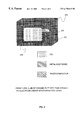
- FIG. 1 This flow chart represents a general perspective of the method used to employ PLZTs as a dynamic holographic medium.
- FIG. 2 This is a representation of the “front view” of a slab of ceramic PLZT.
- FIG. 3 This is ea representation of the “rear view” of a slab of ceramic PLZT.
- FIG. 4 This represents a enlarged view, depicting alignment of index axis in individual material grains in response to an applied poling electric field.
- PLZT is a Lanthanum enhanced lead zirconate titanate material. It is piezo-electric/optic ceramic material. It would now be helpful to the understanding of the present invention to describe the composition and nature of this PLZT ceramic material.
- LCD A liquid Crystal Display (LCD) is a type of display that uses a compound having polar molecular structure, sandwiched between two transparent electrodes. When an electric field is applied, the molecules align within the field, forming a crystalline arrangement that polarizes the light passing through it. A polarized filter laminated over the electrodes blocks polarized light. In this way, a grid of electrodes can selectively “turn on” a cell or a pixel, containing the liquid crystal material, turning it dark. If desired, some types of liquid crystal displays, employ an electro-luminescent panel placed behind the screen to illuminate it. This is commonly referred to as a “backlight” screen. It is used to improve readability but represents a disadvantage since it represents a cost of drawing more power.
- Delta Image represents notion display compression or band width limiting, based upon processing only differences between successive frames.
- Phase Mode This represents the use of an electro-optic material in a mode in which the index variation leads to a variation in the phase of the optical wave going through the material.
- Scattering Mode This represents the use of an electro-optical material in a mode in which scattering is induced at material grain boundaries due to abrupt changes in refractive index at the grain boundaries. Scattering means a directed ray's energy is redistributed through a different path or space than before the event.
- FIG. 1 flow chart represents a general perspective of the method used to employ the PLZT a dynamic holographic display medium. It can be seen that the process is initiated at 100 to employ the PLZT as a dynamic holographic display medium at 101 . The process is continued by employing viewing optics with non-memory display medium at 102 . This is followed by displaying FFT computer generated holograms at 103 .
- the query is then raised at 103 as to whether the user wishes to generate faster and refreshed images at 204 . If the answer to 104 is no, then the process is complected and the process ends at 106 .
- FIG. 2 represents the “front view” of a slab of ceramic PLZT at 200 , with transparent indium-tin-oxide (ITO) electrode at 201 , over photoconductive layer at 203 . Another electrode 204 is also shown.
- FIG. 3 is a representation of the “rear view” of a slab at 300 , with transparent ITO electrode at 301 and another electrode 302 .
- FIG. 4 shows the slab ceramic material at 400 represents an enlarged view from 401 to the enlarged view at 402 , depicting alignment of index axis at 403 in individual material grains in response to an applied poling electric field.
- the “non-memory” PLZT material employed in the instant invention is a specific material phase in the lanthanum-enhanced lead-zerconate-titinate ceramic system.
- the material may be commercially prepared; it is produced by hot-pressing a mixture of powdered components in the proper ratios.
- This is a writing mode in which refractive index discontinuities at grain boundaries, resulting in scattering. This leads to an apparent dark area in the material.
- a poling field can be selectively applied to sections illuminated by light.
- a holographic interference pattern is thus created in the device when an appropriate bias is applied to the sample via the aforementioned light-controllable electrode and a simple ITO backside ground electrode.
- the light-amplitude pattern is controlled by the presence of this field. i.e. it is erased by relaxation of the applied field.
- the axis of the writing system may be normal to the surface of the plate, though tilted geometries may also be employed.
- EO electro-optic
Abstract
Conventional display technology can be used to display crude computer generated holograms (CGH), and can be extended to moving displays. However, the ones best suited from the standpoint of illumination flexibility, such as the common Liquid Crystal Displays (LCDs), switch very slowly. Thus systems with far better dynamic—rapid response requires very complex drive electronics. A non-memory ceramic PLZT, dynamic holographic display medium, provides much faster response time relative to common LCD technology. This system, which is the major embodiment of the present invention, also exhibits good spatial display capability. The system of the present invention, can display Fast Fourier Transformation (FFT) Computer Generated Holograms (CHHs); thus allowing the use of FFT based manipulation of images. By using a delta image updating in Fourier space, the instant system will speed up image generation significantly; since it is often the case that an object's spatial frequency components change more slowly than its position.
Description
The following six copending six patent applications are all assigned to a common assignee. These are application Ser. No. 09/344,536, filed Jun. 25, 1999, Titled A SYSTEM AND METHOD INVOLVING A REVERSIBLE HOLOGRAPHIC RECORDING MEDIUM; application Ser. No. 09/344,575, filed Jun. 25, 1999, Title: A SYSTEM AND METHOD EMPLOYING DYNAMIC HOLOGRAPHIC DISPLAY MEDIUM; application Ser. No. 09/337,030, filed Jun. 25, 1999, Titled: METHOD AND SYSTEM FOR PREPARING HOLOGRAPHIC FULL-COLOR DISPLAYS; application Ser. No. 09/344,594, filed Jun. 25, 1999, Titled: METHOD AND SYSTEM FOR USE OF A VIRTUAL REALITY HEADSETS BASED ON PLZT HOLOGRAPHIC DISPLAY; application Ser. No. 09/344,591, filed Jun. 25, 1999, Titled: Titled METHOD AND SYSTEM FOR BACKLIGHTING AND DIFFUSION WITH PLZTS; application Ser. No. 09/340,324, filed Jun. 25, 1999, Titled: SYSTEM and METHOD FOR CONTROLLING AND MONITORING OF OPTICAL WAVEGUIDE SIGNALS USING PLZT DEVICES. All six of the above patent applications are related to patent application Ser. No. 09/182,075, filed on Oct. 29, 1998. This copending application, titled “35 mm SLIDE PROJECTION PANEL FOR USE WITH COMMONLY AVAILABLE PROJECTION DEVICES” and is hereby incorporated by reference into the above referenced six inventions.
Current holographic recording media exhibit several problems. A hologram is a three-dimensional image record created by holography; a method of reproducing light interference patterns on a medium such as photographic film, creating a hologram. The hologram consists of a light interference pattern preserved in a medium such as photographic film. When suitably illuminated, it produces an image that changes its appearance as the viewer changes their viewing angle.
The present invention based on a novel recording material. PLZT serves as the basis of the present application and is a Lanthanum enhanced lead zirconate titanate composition.
At this point it would be useful, with regard to the present invention, to discuss related art. A search of this art has noted the following patent references. A careful review of these patents, readily distinguishes present invention from any of this earlier art.
U.S. Pat. No. 5,608,554—This reference pertains only to a 2D-Display medium and uses non-coherent light sources. It does not employ Holography or 3D
U.S. Pat. No. 5,122,882 This reference pertains to 2D-animated display medium (no 3D or holography involved). In addition it utilizes a white light source and a simulated display.
U.S. Pat. No. 5,122,890 This reference is similar to the above reference U.S. Pat. No. 5,122,882. It represents a 2D-animated display (no 3D or holography involved)and utilizes a white light source and a simulated display.
U.S. Pat. No. 5,517,278 This patent represents a 2D display device for video camera viewfinder and is not used for holography. It uses a non-coherent light source.
U.S. Pat. No. 5,440,428 This reference is totally unrelated to the present invention. It is for an improved automotive (heads-up display, is not a holographic 3D display medium. It represents a mirror system (can utilize a permanent holographic narrow band reflecting mirror) and no PLZTs used.
U.S. Pat. No. 5,589,980 This patent represents a 2D or simulated 3D display (not holographic). It uses layered images in a projection system to simulate 3D and is completely different from the present application.
U.S. Pat. No. 5,552,840 This reference utilizes stereoscopic vision to simulate a 3D image (uses parallax). No holography used and it uses S and P polarized light to provide stereoscopic images and eyeglasses that separate the light for left and right eye viewing. It is completely different from the present invention.
IBM Technical Disclosure Bulletin vol28 no.6 November 1985 Uses PLZTs for color filters and not a holographic display medium. This is not a display system.
Japanese Patent No.JP60006922A This patent employs Optical control element to make high-speed optical shutters and has nothing to do with a holographic display.
Japanese Patent No. JP59018932A Represents an Optical deflecting device and has nothing to with holographic displays.
As noted in the above referenced copending patent application, Ser. No. 09/182,075, filed on Oct. 29, 1998, describes a PLZT inorganic material. This PLZT material serves as the basis of the present application and is a Lanthanum enhanced lead zirconate titanate material. It is piezoelectric/optic ceramic material. It would now be helpful to the understanding of the present invention to describe the composition and nature of this PLZT ceramic material.
PLZT can be prepared in the following two ways. In one case a mixed oxide(MO) and in the other case chemically prepared (CP). The applicant used, the mixed oxide process to prepare the PLZTs. The mixed oxide (MO) is prepared by wet mixing the oxide powers of Lead (PbO). lanthanum (La2O3), Zirconium (ZrO2) and Titanium (TiO2). The mixture is then dried, calcined (a high temperature solid state chemical reaction), then milled to reduce the particle size to a desired level. A slug is then created by cold pressing, and then a wafer can be formed from the slug by hot pressing. The wafer thus produced is then sliced and polished for use as the panels for the liquid display. The wafer can be up to 15 cm in diameter and from 0.5 mm up to several millimeters in thickness after polishing. It consists of a uniform microstructure of controlled grain size of approximately 2 to 15 um. The grain size is important, as it places a lower limit on how close the controlling electric fields can be and thus limits the pixel size.
While Lanthanum Oxide is preferred, it should be noted that this invention is not necessarily limited to Lanthanum Oxide. Rather Lanthanum Oxide can be replace with other oxides in the PERIODIC TABLE of ELEMENTS, within the “LANTHANIDE Series”. This includes Cerium Ce, Praseodymium Pr, Neodymium Nd, Promethium Pm, Samarium Sm, Europium Eu, Gadolinium Gd, Terbium Tb, Dysprosium Dy, Holmium Ho, thulium tm, Ytterbium Yb, Lutetium Lu.
Conventional display technology can be used to display crude computer generated holograms (CGH), and can be extended to moving displays. However, the ones best suited from the standpoint of illumination flexibility, such as the common Liquid Crystal Displays (LCDs), switch very slowly. Thus systems with far better dynamic—rapid response requires very complex drive electronics.
A non-memory PLZT, dynamic holographic display medium, provides much faster response time relative to common LCD technology. This system, which is the major embodiment of the present invention, also exhibits good spatial display capability. The system of the present invention, can display Fast Fourier Transformation (FFT) Computer Generated Holograms (CHHs); thus allowing the use of FFT based manipulation of images.
By using a delta image updating in Fourier space, the instant system will speed up image generation significantly; since it is often the case that an object's spatial frequency components change more slowly than its position. In addition, apparent changes in size due to perspective can be handled using 3-Dimensional Fourier manipulation so that the display generation of true-size invariant objects is complete in the Fourier domain.
FIG. 1 This flow chart represents a general perspective of the method used to employ PLZTs as a dynamic holographic medium.
FIG. 2 This is a representation of the “front view” of a slab of ceramic PLZT.
FIG. 3 This is ea representation of the “rear view” of a slab of ceramic PLZT.
FIG. 4 This represents a enlarged view, depicting alignment of index axis in individual material grains in response to an applied poling electric field.
It would be beneficial, at this point, to first define certain terms, which would be useful and used in the discussion of the details of this invention.
Glossary of terms
PLZT: is a Lanthanum enhanced lead zirconate titanate material. It is piezo-electric/optic ceramic material. It would now be helpful to the understanding of the present invention to describe the composition and nature of this PLZT ceramic material.
LCD: A liquid Crystal Display (LCD) is a type of display that uses a compound having polar molecular structure, sandwiched between two transparent electrodes. When an electric field is applied, the molecules align within the field, forming a crystalline arrangement that polarizes the light passing through it. A polarized filter laminated over the electrodes blocks polarized light. In this way, a grid of electrodes can selectively “turn on” a cell or a pixel, containing the liquid crystal material, turning it dark. If desired, some types of liquid crystal displays, employ an electro-luminescent panel placed behind the screen to illuminate it. This is commonly referred to as a “backlight” screen. It is used to improve readability but represents a disadvantage since it represents a cost of drawing more power.
Delta Image represents notion display compression or band width limiting, based upon processing only differences between successive frames.
Phase Mode: This represents the use of an electro-optic material in a mode in which the index variation leads to a variation in the phase of the optical wave going through the material.
Scattering Mode: This represents the use of an electro-optical material in a mode in which scattering is induced at material grain boundaries due to abrupt changes in refractive index at the grain boundaries. Scattering means a directed ray's energy is redistributed through a different path or space than before the event.
As noted earlier, FIG. 1 flow chart represents a general perspective of the method used to employ the PLZT a dynamic holographic display medium. It can be seen that the process is initiated at 100 to employ the PLZT as a dynamic holographic display medium at 101. The process is continued by employing viewing optics with non-memory display medium at 102. This is followed by displaying FFT computer generated holograms at 103.
The query is then raised at 103 as to whether the user wishes to generate faster and refreshed images at 204. If the answer to 104 is no, then the process is complected and the process ends at 106.
If the answer to 104 is yes, then the process moves on to 105, where the process employs the FFT based manipulation of images to generate faster and refreshed images. Then the process is complected and the process ends at 106
As noted above, FIG. 2 represents the “front view” of a slab of ceramic PLZT at 200, with transparent indium-tin-oxide (ITO) electrode at 201, over photoconductive layer at 203. Another electrode 204 is also shown. FIG. 3 is a representation of the “rear view” of a slab at 300, with transparent ITO electrode at 301 and another electrode 302. FIG. 4 shows the slab ceramic material at 400 represents an enlarged view from 401 to the enlarged view at 402, depicting alignment of index axis at 403 in individual material grains in response to an applied poling electric field.
The “non-memory” PLZT material employed in the instant invention, is a specific material phase in the lanthanum-enhanced lead-zerconate-titinate ceramic system. The material may be commercially prepared; it is produced by hot-pressing a mixture of powdered components in the proper ratios.
A major distinguishing feature of these materials, in addition to the relatively rapid writing response, is the scattering-mode effect observed in them. This is a writing mode in which refractive index discontinuities at grain boundaries, resulting in scattering. This leads to an apparent dark area in the material. Using transparent photoconductive coating on the surface of a plate of the PLZT material, covered with a transparent indium-tin-oxide (ITO) electrode, a poling field can be selectively applied to sections illuminated by light. A holographic interference pattern is thus created in the device when an appropriate bias is applied to the sample via the aforementioned light-controllable electrode and a simple ITO backside ground electrode. The light-amplitude pattern is controlled by the presence of this field. i.e. it is erased by relaxation of the applied field. In this arrangement, the axis of the writing system may be normal to the surface of the plate, though tilted geometries may also be employed.
Since these materials exhibit electro-optic (EO) properties, they may also be used to record phase patterns. To accomplish this, a bias must be selectively applied transverse to the optical axis in the area where a phase shift is desired.
Claims (18)
1. A computer based dynamic holographic display system and medium, comprising:
a non-memory display material means based on PLTZ coated with a transparent photoconductive coating and covered with a transparent indium-tin-oxide electrode;
means for employing viewing optics with said non-memory holographic material, to display Fast Fourier Transformation computer generated holograms;
means of employing said Fast Fourier Transformation based manipulation of images to generate faster and refreshed said images, than attainable by Liquid Crystal Display Material.
2. The system of claim 1 wherein said PLTZ based system functions more rapidly than the comparable common Liquid Crystal Display material, for said display purpose.
3. The system of claim 1 wherein said PLTZ based system exhibits spatial display capabilities which are equal to or better than the comparable common Liquid Crystal Display material.
4. The system of claim 1 wherein said PLTZ based system displays Fast Fourier Transformation (FFT) Computer Generated Holograms (CHHs).
5. The system of claim 4 wherein said PLTZ based system displays facilitates the use of Fast Fourier Transformation based manipulation of images.
6. The system of claim 5 wherein said PLTZ based system wherein the use of a delta image updating in Fourier space, speeds up image generation.
7. The system of claim 1 wherein said PLZT holographic medium is derived from a mixture of metal oxides comprising lead, lanthanum, zirconium and titanium.
8. The system of claim 7 wherein said metal oxides are lead oxide (Pbo), lanthanum oxide (La2O3), Titanium Oxide (TiO2) and Zirconium Oxide (ZrO2).
9. The system of claim 8 wherein the Lanthanum Oxide can be replace with any other oxide in the periodic table of elements from the “Lanthanide Series”, which includes Cerium Ce, Praseodymium Pr, Neodymium Nd, Promethium Pm, Samarium Sm, Europium Eu, Gadolinium Gd, Terbium Tb, Dysprosium Dy, Holmium Ho, thulium tm, Ytterbium Yb, Lutetium Lu.
10. A computer based method for employing a dynamic holographic display medium, comprising the steps of:
providing a non-memory display medium based on PLZT, coated with a transparent photoconductive coating and covered with a transparent indium-tin-oxide electrode;
employing viewing optics with said non-memory material, to display Fast Fourier Transformation computer generated holograms;
employing said Fast Fourier Transformation based manipulation of images to generate faster and refreshed said images, than attainable by Liquid Crystal Display Material.
11. The method of claim 10 further comprising the steps of:
using said PLTZ based method to attain more rapid displays than the comparable common Liquid Crystal Display material can provide for display purpose.
12. The method of claim 10 further comprising the steps of:
employing said PLTZ based method to attain spatial display capabilities which are equal to or better than the comparable common Liquid Crystal Display material.
13. The method of claim 10, further comprising the steps of:
employing said PLTZ based method for displaying said Fast Fourier Transformation (FFT) Computer Generated Holograms (CHHs).
14. The method of claim 13 further comprising the steps of:
wherein said PLTZ based method to facilitate the use of said Fast Fourier Transformation based image manipulation.
15. The method of claim 10 further comprising the steps of:
using said PLTZ based method of a delta image updating in Fourier space, to speed up image generation.
16. The method of claim 10 further comprising the steps of:
employing said PLZT non-memory material, which is derived from a mixture of metal oxides comprising lead, lanthanum, zirconium and titanium.
17. The method of claim 16 wherein said metal oxides are lead oxide (Pbo), lanthanum oxide (La2O3), Titanium Oxide (TiO2) and Zirconium Oxide (ZrO2).
18. The method of claim 17 wherein the Lanthanum Oxide can be replace with any other oxide in the periodic table of elements from the “Lanthanide Series”, which includes Cerium Ce, Praseodymium Pr, Neodymium Nd, Promethium Pm, Samarium Sm, Europium Eu, Gadolinium Gd, Terbium Tb, Dysprosium Dy, Holmium Ho, thulium tm, Ytterbium Yb, Lutetium Lu.
Priority Applications (5)
| Application Number | Priority Date | Filing Date | Title |
|---|---|---|---|
| US09/344,595 US6178018B1 (en) | 1999-06-25 | 1999-06-25 | Process and method employing dynamic holographic display medium |
| TW089109927A TW579458B (en) | 1999-06-25 | 2000-05-23 | A process and method employing dynamic holographic display medium |
| KR1020000032633A KR100349226B1 (en) | 1999-06-25 | 2000-06-14 | A system and method employing dynamic holographic display medium |
| CNB00118606XA CN1137395C (en) | 1999-06-25 | 2000-06-16 | Technology and method for displaying medium by dynamic holography |
| JP2000185750A JP2001042755A (en) | 1999-06-25 | 2000-06-21 | Process and method using dynamic holography display medium |
Applications Claiming Priority (1)
| Application Number | Priority Date | Filing Date | Title |
|---|---|---|---|
| US09/344,595 US6178018B1 (en) | 1999-06-25 | 1999-06-25 | Process and method employing dynamic holographic display medium |
Publications (1)
| Publication Number | Publication Date |
|---|---|
| US6178018B1 true US6178018B1 (en) | 2001-01-23 |
Family
ID=23351186
Family Applications (1)
| Application Number | Title | Priority Date | Filing Date |
|---|---|---|---|
| US09/344,595 Expired - Lifetime US6178018B1 (en) | 1999-06-25 | 1999-06-25 | Process and method employing dynamic holographic display medium |
Country Status (5)
| Country | Link |
|---|---|
| US (1) | US6178018B1 (en) |
| JP (1) | JP2001042755A (en) |
| KR (1) | KR100349226B1 (en) |
| CN (1) | CN1137395C (en) |
| TW (1) | TW579458B (en) |
Cited By (5)
| Publication number | Priority date | Publication date | Assignee | Title |
|---|---|---|---|---|
| US20050286101A1 (en) * | 2004-04-13 | 2005-12-29 | Board Of Regents, The University Of Texas System | Holographic projector |
| US20070285763A1 (en) * | 2006-06-09 | 2007-12-13 | Kewen Kevin Li | Electro-optic gain ceramic and lossless devices |
| US20080066527A1 (en) * | 2004-11-12 | 2008-03-20 | Vfs Technologies Limited | Method and apparatus for determining flow |
| USRE41567E1 (en) * | 2000-08-10 | 2010-08-24 | Jenn-Tsair Tsai | Method for optimizing the best resolution of an optical scanning system and apparatus for the same |
| US10321159B2 (en) | 2015-08-27 | 2019-06-11 | Samsung Electronics Co., Ltd. | Apparatus and method of performing fourier transform |
Families Citing this family (1)
| Publication number | Priority date | Publication date | Assignee | Title |
|---|---|---|---|---|
| CN104761106B (en) * | 2015-04-27 | 2017-12-19 | 上海博亚环保科技有限公司 | Sewage disposal system and sewage water treatment method |
Citations (12)
| Publication number | Priority date | Publication date | Assignee | Title |
|---|---|---|---|---|
| JPS5918932A (en) | 1982-07-23 | 1984-01-31 | Matsushita Electric Ind Co Ltd | Optical deflecting device |
| JPS606922A (en) | 1983-06-24 | 1985-01-14 | Matsushita Electric Ind Co Ltd | Thin-film optical control element |
| US5020882A (en) | 1987-11-06 | 1991-06-04 | Makow David M | Electro-optic animated displays and indicators |
| US5221989A (en) * | 1991-11-13 | 1993-06-22 | Northrop Corporation | Longitudinal plzt spatial light modulator |
| US5303043A (en) * | 1992-09-01 | 1994-04-12 | Florida Atlantic University | Projection television display utilizing Bragg diffraction cell for producing horizontal scan |
| US5440428A (en) | 1993-09-30 | 1995-08-08 | Hughes Aircraft Company | Automotive instrument 3-D virtual image display |
| US5517278A (en) | 1991-06-12 | 1996-05-14 | Matsushita Electric Industrial Co., Ltd. | Viewfinder for video cameras |
| US5552840A (en) | 1992-03-13 | 1996-09-03 | Sharp Kabushiki Kaisha | Three dimensional projection display reflecting divided polarized light on to reflective liquid crystal display elements |
| US5564810A (en) | 1992-12-31 | 1996-10-15 | Honeywell Inc. | Full color stereoscopic display with color multiplexing |
| US5589980A (en) | 1989-02-27 | 1996-12-31 | Bass; Robert | Three dimensional optical viewing system |
| US5608554A (en) | 1994-07-26 | 1997-03-04 | Samsung Display Devices Co., Ltd. | LCD having a phosphor layer and a backlight source with a main emitting peak in the region of 380-420nm |
| US5798864A (en) * | 1994-03-24 | 1998-08-25 | Olympus Optical Co., Ltd. | Projection type image display apparatus |
-
1999
- 1999-06-25 US US09/344,595 patent/US6178018B1/en not_active Expired - Lifetime
-
2000
- 2000-05-23 TW TW089109927A patent/TW579458B/en not_active IP Right Cessation
- 2000-06-14 KR KR1020000032633A patent/KR100349226B1/en not_active IP Right Cessation
- 2000-06-16 CN CNB00118606XA patent/CN1137395C/en not_active Expired - Fee Related
- 2000-06-21 JP JP2000185750A patent/JP2001042755A/en active Pending
Patent Citations (13)
| Publication number | Priority date | Publication date | Assignee | Title |
|---|---|---|---|---|
| JPS5918932A (en) | 1982-07-23 | 1984-01-31 | Matsushita Electric Ind Co Ltd | Optical deflecting device |
| JPS606922A (en) | 1983-06-24 | 1985-01-14 | Matsushita Electric Ind Co Ltd | Thin-film optical control element |
| US5020882A (en) | 1987-11-06 | 1991-06-04 | Makow David M | Electro-optic animated displays and indicators |
| US5122890A (en) | 1987-11-06 | 1992-06-16 | Makow David M | Electro-optic animated displays and indicators employing electro-optical cells and mosaic segment polarizer |
| US5589980A (en) | 1989-02-27 | 1996-12-31 | Bass; Robert | Three dimensional optical viewing system |
| US5517278A (en) | 1991-06-12 | 1996-05-14 | Matsushita Electric Industrial Co., Ltd. | Viewfinder for video cameras |
| US5221989A (en) * | 1991-11-13 | 1993-06-22 | Northrop Corporation | Longitudinal plzt spatial light modulator |
| US5552840A (en) | 1992-03-13 | 1996-09-03 | Sharp Kabushiki Kaisha | Three dimensional projection display reflecting divided polarized light on to reflective liquid crystal display elements |
| US5303043A (en) * | 1992-09-01 | 1994-04-12 | Florida Atlantic University | Projection television display utilizing Bragg diffraction cell for producing horizontal scan |
| US5564810A (en) | 1992-12-31 | 1996-10-15 | Honeywell Inc. | Full color stereoscopic display with color multiplexing |
| US5440428A (en) | 1993-09-30 | 1995-08-08 | Hughes Aircraft Company | Automotive instrument 3-D virtual image display |
| US5798864A (en) * | 1994-03-24 | 1998-08-25 | Olympus Optical Co., Ltd. | Projection type image display apparatus |
| US5608554A (en) | 1994-07-26 | 1997-03-04 | Samsung Display Devices Co., Ltd. | LCD having a phosphor layer and a backlight source with a main emitting peak in the region of 380-420nm |
Non-Patent Citations (1)
| Title |
|---|
| IBM Technical Disclosure Bulletin, vol. 28, No. 6, Nov. 1985 "Frame-Sequential Electronic Color Display Filters". |
Cited By (8)
| Publication number | Priority date | Publication date | Assignee | Title |
|---|---|---|---|---|
| USRE41567E1 (en) * | 2000-08-10 | 2010-08-24 | Jenn-Tsair Tsai | Method for optimizing the best resolution of an optical scanning system and apparatus for the same |
| US20050286101A1 (en) * | 2004-04-13 | 2005-12-29 | Board Of Regents, The University Of Texas System | Holographic projector |
| US7738151B2 (en) * | 2004-04-13 | 2010-06-15 | Board Of Regents, The University Of Texas System | Holographic projector |
| US20080066527A1 (en) * | 2004-11-12 | 2008-03-20 | Vfs Technologies Limited | Method and apparatus for determining flow |
| US20100319465A1 (en) * | 2004-11-12 | 2010-12-23 | Vfs Technologies Limited | Method and apparatus for determining flow |
| US8065922B2 (en) | 2004-11-12 | 2011-11-29 | Vfs Technologies Limited | Flow metering device for an aspirated smoke detector |
| US20070285763A1 (en) * | 2006-06-09 | 2007-12-13 | Kewen Kevin Li | Electro-optic gain ceramic and lossless devices |
| US10321159B2 (en) | 2015-08-27 | 2019-06-11 | Samsung Electronics Co., Ltd. | Apparatus and method of performing fourier transform |
Also Published As
| Publication number | Publication date |
|---|---|
| JP2001042755A (en) | 2001-02-16 |
| TW579458B (en) | 2004-03-11 |
| KR20010007364A (en) | 2001-01-26 |
| CN1137395C (en) | 2004-02-04 |
| CN1285519A (en) | 2001-02-28 |
| KR100349226B1 (en) | 2002-08-19 |
Similar Documents
| Publication | Publication Date | Title |
|---|---|---|
| US5784139A (en) | Image display device | |
| US3836243A (en) | Liquid crystal display apparatus | |
| US7486350B2 (en) | Display device, viewing angle control device, electronic display device, and multiple image display device | |
| TWI309738B (en) | ||
| US8184145B2 (en) | Display device and electronic apparatus | |
| TW548487B (en) | Single cell liquid crystal shutter glasses | |
| JP2002189230A (en) | Liquid crystal display device and stereoscopic display device | |
| CN112379550A (en) | Display panel, driving method and display device | |
| CN112666747B (en) | Display panel, driving method and display device | |
| KR100682202B1 (en) | Method for forming inorganic alignment film | |
| EP1644773A1 (en) | Illumination system | |
| JPS59216126A (en) | Optical recording element and its recording method | |
| CN108051946A (en) | A kind of display device | |
| US6178018B1 (en) | Process and method employing dynamic holographic display medium | |
| US7701532B2 (en) | Sight controllable display device and terminal having the same | |
| Gong et al. | Static volumetric three-dimensional display based on an electric-field-controlled two-dimensional optical beam scanner | |
| TWI777794B (en) | Switchable light filter and its use | |
| JP2007249125A (en) | Viewing angle controlled display device and terminal equipment provided therewith | |
| JP2721357B2 (en) | Liquid crystal device | |
| JPH0876114A (en) | Liquid crystal display and back light thereof | |
| Andreev et al. | Electric-field-controlled light scattering in ferroelectric liquid crystals | |
| KR20080108770A (en) | Liquid crystal display device switchable between reflective mode and transmissive mode employing an active reflective polarizer | |
| JPH1026766A (en) | Liquid crystal display device | |
| CN218068504U (en) | Display panel and display device | |
| Yamagishi et al. | A multicolor projection display using nematic-cholesteric liquid crystal |
Legal Events
| Date | Code | Title | Description |
|---|---|---|---|
| AS | Assignment |
Owner name: IBM CORPORATION, NEW YORK Free format text: ASSIGNMENT OF ASSIGNORS INTEREST;ASSIGNORS:KEKAS, DENNIS JASON;HERLOCKER, JON ALAN;LOEB, MITCHELL LEVY;REEL/FRAME:010069/0491;SIGNING DATES FROM 19990622 TO 19990624 |
|
| STCF | Information on status: patent grant |
Free format text: PATENTED CASE |
|
| FPAY | Fee payment |
Year of fee payment: 4 |
|
| FPAY | Fee payment |
Year of fee payment: 8 |
|
| REMI | Maintenance fee reminder mailed | ||
| FPAY | Fee payment |
Year of fee payment: 12 |
|
| SULP | Surcharge for late payment |
Year of fee payment: 11 |