US6177703B1 - Method and apparatus for producing a single polysilicon flash EEPROM having a select transistor and a floating gate transistor - Google Patents
Method and apparatus for producing a single polysilicon flash EEPROM having a select transistor and a floating gate transistor Download PDFInfo
- Publication number
- US6177703B1 US6177703B1 US09/321,792 US32179299A US6177703B1 US 6177703 B1 US6177703 B1 US 6177703B1 US 32179299 A US32179299 A US 32179299A US 6177703 B1 US6177703 B1 US 6177703B1
- Authority
- US
- United States
- Prior art keywords
- floating gate
- transistor
- flash
- memory cell
- cell
- Prior art date
- Legal status (The legal status is an assumption and is not a legal conclusion. Google has not performed a legal analysis and makes no representation as to the accuracy of the status listed.)
- Expired - Fee Related
Links
- 238000007667 floating Methods 0.000 title claims abstract description 42
- 229910021420 polycrystalline silicon Inorganic materials 0.000 title claims description 9
- 229920005591 polysilicon Polymers 0.000 title claims description 8
- 238000000034 method Methods 0.000 title description 20
- 230000015654 memory Effects 0.000 claims abstract description 28
- 239000000758 substrate Substances 0.000 claims abstract description 26
- 230000005641 tunneling Effects 0.000 claims abstract description 22
- 230000008878 coupling Effects 0.000 claims abstract description 16
- 238000010168 coupling process Methods 0.000 claims abstract description 16
- 238000005859 coupling reaction Methods 0.000 claims abstract description 16
- 239000010410 layer Substances 0.000 claims 2
- 239000002356 single layer Substances 0.000 claims 1
- 238000005516 engineering process Methods 0.000 abstract description 40
- 230000006870 function Effects 0.000 abstract description 11
- 230000008569 process Effects 0.000 description 13
- 239000007943 implant Substances 0.000 description 7
- 230000005684 electric field Effects 0.000 description 6
- 239000002784 hot electron Substances 0.000 description 5
- VYPSYNLAJGMNEJ-UHFFFAOYSA-N Silicium dioxide Chemical compound O=[Si]=O VYPSYNLAJGMNEJ-UHFFFAOYSA-N 0.000 description 4
- 239000003990 capacitor Substances 0.000 description 4
- 150000004767 nitrides Chemical class 0.000 description 4
- 239000004065 semiconductor Substances 0.000 description 4
- OAICVXFJPJFONN-UHFFFAOYSA-N Phosphorus Chemical compound [P] OAICVXFJPJFONN-UHFFFAOYSA-N 0.000 description 3
- XUIMIQQOPSSXEZ-UHFFFAOYSA-N Silicon Chemical compound [Si] XUIMIQQOPSSXEZ-UHFFFAOYSA-N 0.000 description 3
- 230000004888 barrier function Effects 0.000 description 3
- 230000015572 biosynthetic process Effects 0.000 description 3
- 230000010354 integration Effects 0.000 description 3
- 230000000873 masking effect Effects 0.000 description 3
- 229910052698 phosphorus Inorganic materials 0.000 description 3
- 239000011574 phosphorus Substances 0.000 description 3
- 230000009467 reduction Effects 0.000 description 3
- 229910052710 silicon Inorganic materials 0.000 description 3
- 239000010703 silicon Substances 0.000 description 3
- 239000000126 substance Substances 0.000 description 3
- 230000015556 catabolic process Effects 0.000 description 2
- 229910052681 coesite Inorganic materials 0.000 description 2
- 229910052906 cristobalite Inorganic materials 0.000 description 2
- 238000011161 development Methods 0.000 description 2
- 238000002347 injection Methods 0.000 description 2
- 239000007924 injection Substances 0.000 description 2
- 238000002955 isolation Methods 0.000 description 2
- 238000004519 manufacturing process Methods 0.000 description 2
- 229910052751 metal Inorganic materials 0.000 description 2
- 239000002184 metal Substances 0.000 description 2
- 229910021421 monocrystalline silicon Inorganic materials 0.000 description 2
- 230000001590 oxidative effect Effects 0.000 description 2
- 230000002829 reductive effect Effects 0.000 description 2
- 239000000377 silicon dioxide Substances 0.000 description 2
- 125000006850 spacer group Chemical group 0.000 description 2
- 229910052682 stishovite Inorganic materials 0.000 description 2
- 229910052905 tridymite Inorganic materials 0.000 description 2
- WFKWXMTUELFFGS-UHFFFAOYSA-N tungsten Chemical compound [W] WFKWXMTUELFFGS-UHFFFAOYSA-N 0.000 description 2
- 229910052721 tungsten Inorganic materials 0.000 description 2
- 239000010937 tungsten Substances 0.000 description 2
- 229910000838 Al alloy Inorganic materials 0.000 description 1
- ZOXJGFHDIHLPTG-UHFFFAOYSA-N Boron Chemical compound [B] ZOXJGFHDIHLPTG-UHFFFAOYSA-N 0.000 description 1
- 230000005689 Fowler Nordheim tunneling Effects 0.000 description 1
- 229910052581 Si3N4 Inorganic materials 0.000 description 1
- ATJFFYVFTNAWJD-UHFFFAOYSA-N Tin Chemical compound [Sn] ATJFFYVFTNAWJD-UHFFFAOYSA-N 0.000 description 1
- 238000012443 analytical study Methods 0.000 description 1
- 238000003491 array Methods 0.000 description 1
- 229910052785 arsenic Inorganic materials 0.000 description 1
- RQNWIZPPADIBDY-UHFFFAOYSA-N arsenic atom Chemical compound [As] RQNWIZPPADIBDY-UHFFFAOYSA-N 0.000 description 1
- 125000004429 atom Chemical group 0.000 description 1
- 229910052796 boron Inorganic materials 0.000 description 1
- 238000004364 calculation method Methods 0.000 description 1
- 238000005229 chemical vapour deposition Methods 0.000 description 1
- 230000000295 complement effect Effects 0.000 description 1
- 239000013078 crystal Substances 0.000 description 1
- 238000013500 data storage Methods 0.000 description 1
- 238000009792 diffusion process Methods 0.000 description 1
- 230000000694 effects Effects 0.000 description 1
- 125000005843 halogen group Chemical group 0.000 description 1
- 229910044991 metal oxide Inorganic materials 0.000 description 1
- 150000004706 metal oxides Chemical class 0.000 description 1
- 230000003647 oxidation Effects 0.000 description 1
- 238000007254 oxidation reaction Methods 0.000 description 1
- 230000036961 partial effect Effects 0.000 description 1
- 238000000206 photolithography Methods 0.000 description 1
- 229920002120 photoresistant polymer Polymers 0.000 description 1
- 238000001020 plasma etching Methods 0.000 description 1
- 238000009877 rendering Methods 0.000 description 1
- 230000000717 retained effect Effects 0.000 description 1
- 238000000926 separation method Methods 0.000 description 1
- 238000004088 simulation Methods 0.000 description 1
- 239000007787 solid Substances 0.000 description 1
- 230000003068 static effect Effects 0.000 description 1
- 230000001052 transient effect Effects 0.000 description 1
Images


Classifications
-
- H—ELECTRICITY
- H10—SEMICONDUCTOR DEVICES; ELECTRIC SOLID-STATE DEVICES NOT OTHERWISE PROVIDED FOR
- H10B—ELECTRONIC MEMORY DEVICES
- H10B41/00—Electrically erasable-and-programmable ROM [EEPROM] devices comprising floating gates
- H10B41/30—Electrically erasable-and-programmable ROM [EEPROM] devices comprising floating gates characterised by the memory core region
-
- H—ELECTRICITY
- H01—ELECTRIC ELEMENTS
- H01L—SEMICONDUCTOR DEVICES NOT COVERED BY CLASS H10
- H01L29/00—Semiconductor devices adapted for rectifying, amplifying, oscillating or switching, or capacitors or resistors with at least one potential-jump barrier or surface barrier, e.g. PN junction depletion layer or carrier concentration layer; Details of semiconductor bodies or of electrodes thereof ; Multistep manufacturing processes therefor
- H01L29/66—Types of semiconductor device ; Multistep manufacturing processes therefor
- H01L29/68—Types of semiconductor device ; Multistep manufacturing processes therefor controllable by only the electric current supplied, or only the electric potential applied, to an electrode which does not carry the current to be rectified, amplified or switched
- H01L29/76—Unipolar devices, e.g. field effect transistors
- H01L29/772—Field effect transistors
- H01L29/78—Field effect transistors with field effect produced by an insulated gate
- H01L29/788—Field effect transistors with field effect produced by an insulated gate with floating gate
-
- H—ELECTRICITY
- H10—SEMICONDUCTOR DEVICES; ELECTRIC SOLID-STATE DEVICES NOT OTHERWISE PROVIDED FOR
- H10B—ELECTRONIC MEMORY DEVICES
- H10B41/00—Electrically erasable-and-programmable ROM [EEPROM] devices comprising floating gates
- H10B41/60—Electrically erasable-and-programmable ROM [EEPROM] devices comprising floating gates the control gate being a doped region, e.g. single-poly memory cell
-
- H—ELECTRICITY
- H10—SEMICONDUCTOR DEVICES; ELECTRIC SOLID-STATE DEVICES NOT OTHERWISE PROVIDED FOR
- H10B—ELECTRONIC MEMORY DEVICES
- H10B69/00—Erasable-and-programmable ROM [EPROM] devices not provided for in groups H10B41/00 - H10B63/00, e.g. ultraviolet erasable-and-programmable ROM [UVEPROM] devices
-
- H—ELECTRICITY
- H10—SEMICONDUCTOR DEVICES; ELECTRIC SOLID-STATE DEVICES NOT OTHERWISE PROVIDED FOR
- H10B—ELECTRONIC MEMORY DEVICES
- H10B99/00—Subject matter not provided for in other groups of this subclass
Definitions
- the present invention is generally directed to semiconductor memories, and more particularly, to the development of memory cells which can be easily integrated with high performance logic technologies.
- DRAMs dynamic random access memories
- SRAMs static random access memories
- ROMs read-only memories
- EEPROMs electrically erasable programmable read-only memories
- flash EEPROMs flash EEPROMs into high performance logic technologies.
- DRAMs dynamic random access memories
- SRAMs static random access memories
- ROMs read-only memories
- EEPROMs electrically erasable programmable read-only memories
- flash EEPROMs flash erasable programmable read-only memories
- flash EEPROMs flash erasable programmable read-only memories
- CMOS complementary metal oxide semiconductor
- the applications for such an integrated technology include software updates, storing identification codes, system reconfiguration in the field, look-up tables, manufacturing codes, non-volatile data storage, smart cards which use flash embedded memory, prototyping and various programmable logic devices and field programmable gate arrays.
- CMOS devices complementary metal-oxide-semiconductor-semiconductor-semiconductor-semiconductor-semiconductor-semiconductor-semiconductor-semiconductor-semiconductor-semiconductor-semiconductor-semiconductor-semiconductor-semiconductor-semiconductor cell; and (4) cells which use edges for control or select gates.
- flash memory cells which form self-aligned trenches at the edge of a partially formed stack-gate structure.
- each of these technologies suffers drawbacks which inhibits their straightforward, easy integration into high performance logic technologies.
- FIG. 1A illustrates features of a 0.18 ⁇ m state-of-the-art high performance logic process which uses approximately 20 photolithography steps, and some five levels of interconnect. It would be desirable to formulate a flash-EEPROM cell and technology suitable for embedded applications, which requires a minimum perturbation to the high performance logic technology, and which does not compromise logic function performance.
- the EEPROM cell should be compatible with deep submicron dimensions and technology.
- STI shallow-trench isolation
- CMP chemical mechanical polish
- transistor length L 0.18 to 0.25 ⁇ m
- salicides usually Ti-based
- V d 1.8-2.5V
- tungsten plugs with Ti/TiN liner aluminum alloy interconnects with Ti/TiN barrier and TiN ARC
- silicon nitride spacers for lightly doped drains and dual-poly gate electrodes (p+ for p-channel and n+ for n-channel).
- SAC Self-aligned contacts
- borderless contacts are generally seen in DRAMs and SRAMs at this technology level.
- a programming time of about 10 ⁇ 5 seconds is possible for commodity flash memories using technologies below 0.5 ⁇ m. See, for example, R. Bez, et al, “The channel hot electron programming of a floating gate MOSFET: An analytical study”, 12 th Nonvolatile Semiconductor Memory Workshop, Monterey, Calif., August 1992 via Paolo Pavan, et al, “Flash Memory Cells-An Overview”, Proc. IEEE, 85, No. 8, August 1997, page 1248. With this speed, the programming of one million bits would require about 10 seconds.
- a maximum cell size of about 40 f 2 would be desirable, wherein the parameter f is the minimum feature size.
- 2 Mbits of flash memory of this cell size would occupy only about 5% (core area only) of a 1 cm 2 chip.
- single-poly flash EEPROM cells are known, they are relatively large, and are not easily integrated into a high performance technology.
- a single-poly flash EEPROM cell is disclosed in “An EEPROM for Microprocessor and Custom Logic”, by Cuppens, R., IEEE J. of Solid state Circuits, Vol. SC-20, No. 2, April 1985, page 603.
- This cell couples an n+ region in the substrate to a leg of the floating gate. By applying 13V to the n+, via a metal contact, electrons can be drawn from a thin oxide “injector” region “D”.
- the cell area is very large (i.e., approximately 140 f 2 ).
- Another single poly EEPROM cell disclosed in U.S. Pat. No. 5,132,239 has a selection transistor and a floating gate which is capacitively coupled to an n+ region.
- the cell has a thin oxide region for tunneling electrons.
- the cell is erased by taking the bit line to ground and the control gate high. Electrons flow to the floating gate, turning off a second transistor connected in series to the selection transistor.
- the cell is programmed by pulsing the bit line high while holding the control gate at ground. Electrons flow from the floating gate lowering the threshold voltage and turning on the second transistor.
- the area is roughly 100 f 2 , which is relatively large.
- the known single poly cells use a selection transistor (forming a two transistor cell), and thereby free the device of the over erase problem typical of the two-poly single-transistor stacked gate cells.
- known single poly cells both program and erase through the thin tunneling oxide.
- these cells have both “injector” and floating gate regions between the source and drain of the selection transistors, which increases the cell area.
- exemplary embodiments of the present invention are directed to single poly flash EEPROM cells which avoid the drawbacks of conventional two poly stacked gate cells, and which are easily integrated with high performance logic technologies.
- An exemplary two transistor flash-EEPROM memory cell array comprises a plurality of these flash EEPROM cells, each having a select transistor with a bit line and a word line, where the select transistor is in series with a floating gate transistor.
- the floating gate transistor has a thin tunneling oxide formed on a textured monocrystalline substrate.
- the floating gate is also formed over a heavily doped region in the substrate which forms a coupling line capacitively coupled to the floating gate, and which performs a tunneling function.
- Exemplary embodiments use only one floating gate electrode between the source and drain, giving a simpler and smaller cell. Exemplary embodiments also use textured substrate tunnel-oxide technology to significantly lower programming and erase voltages, thus increasing the compatibility of flash-EEPROM technology to deep sub-micron higher performance logic processes.
- An exemplary method of forming a single-poly, textured substrate two-transistor flash-EEPROM memory cell array comprises establishing a select transistor with a bit line and a word line on a substrate, establishing a floating gate transistor in series with said select transistor on said substrate, forming a thin tunneling oxide on a textured monocrystalline substrate, with the floating gate transistor placed over a heavily doped region in the substrate and forming, with the heavily doped region, a coupling line which is capacitively coupled to said floating gate which performs a tunneling function.
- exemplary embodiments of the present invention relate to a flash-EEPROM memory cell, and process for producing such a memory cell, wherein the memory cell includes: a select transistor formed from a first polysilicon layer with a bit line and a word line; a floating gate transistor formed from said first polysilicon layer, connected in series with said select transistor, said floating gate transistor having a tunneling oxide formed on a textured monocrystalline substrate; and a heavily doped region formed in said substrate, said floating gate being formed over said heavily doped region, said heavily doped region forming a coupling line capacitively coupled to said floating gate.
- a select transistor formed from a first polysilicon layer with a bit line and a word line
- a floating gate transistor formed from said first polysilicon layer, connected in series with said select transistor, said floating gate transistor having a tunneling oxide formed on a textured monocrystalline substrate
- a heavily doped region formed in said substrate, said floating gate being formed over said heavily doped region, said heavily doped region forming a coupling line capacit
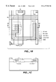
- FIGS. 1 A- 1 C illustrate a conventional high performance logic technology, and a conventional single-poly flash EEPROM cell
- FIGS. 2, 2 A and 2 B illustrate an exemplary single-poly flash EEPROM cell configured in accordance with the present invention
- FIG. 3 illustrates an exemplary single-poly flash EEPROM cell configured with a wider word line and higher coupling ratio in accordance with an exemplary embodiment of the present invention
- FIGS. 4 A- 4 C illustrate exemplary erase, program and read functions for a single-poly flash EEPROM cell configured in accordance with an exemplary embodiment of the present invention.
- Exemplary embodiments of the present invention use Fowler-Nordheim tunneling instead of hot electron channel injection to achieve exemplary programming times of about 5 ⁇ 10 ⁇ 4 to about 10 ⁇ 5 seconds per cell.
- a flash EEPROM cell is compatible with approximately 0.18 ⁇ m high performance logic technology. Gate oxide thicknesses and applied voltages have been selected such that the resulting electric fields do not exceed dielectric breakdown or time-degration limits.
- An exemplary cell of the present invention uses textured substrate tunneling oxides as discussed in Kow-Ming Chang, et al “A New Simple and Reliable Method to Form a Textured Si Surface for the Fabrication of a Tunnel Oxide Film”, IEEE electron Dev. Letters, 19, No. 5, May 1998, pg. 145.
- a tunnel oxide is formed by oxidizing completely through a thin polysilicon film lying directly on monocrystalline silicon. This forms a textured surface on the single crystal substrate. After stripping the oxide, an oxide formed on this roughed silicon exhibits enhanced tunneling currents. Furthermore, the dielectric strength is significantly improved over oxides (poly ox) formed on textured poly.
- FIGS. 2A and 2B show a top side layout and two cross sectional views of one embodiment of a flash cell in accordance with the present invention.
- the process features self-aligned tungsten-plug contacts, double level metal, and shallow trench isolation.
- the cell has an area of about 18 f 2 .
- the n+ substrate area coupled to the poly 1 floating gate is equal to the floating gate tunnel oxide transistor (marked B) area.
- 8V were applied to the n+ control line then the floating gate would go to about 2.5V.
- this would produce an electric field at B over the source line of about 5.0 ⁇ 10 6 V/cm, and a tunneling current of about 5 ⁇ 10 ⁇ 4 A/cm 2 .
- the n+ control line region should have sufficient doping concentration that the surface does not invert at 8V.
- a phosphorus or arsenic concentration of about 10 20 atoms/cm 3 would be more than adequate to prevent inversion.
- an inversion layer positively charged, may be formed under the floating gate (region B) by turning the transistor on and grounding the n+ control and source lines. Since this is in the hard direction of tunneling current flow, about 5V would have to be applied to the bit line and a voltage somewhat over this applied to the word line. For 0.18 ⁇ m technology, such a voltage is close to punch through and junction breakdown conditions. For this reason, FIG. 2 for 0.18 ⁇ m gate length technology, may be somewhat more dense than practicable for some processes.
- the word line width may be simply adjusted upward to 2f, for example, and the cell area would increase to about 22.5 f 2 .
- FIG. 3 Another embodiment of the present invention provides higher coupling, since this would allow a voltage reduction on the n+ coupling line.
- a cell with a higher coupling factor may be seen in FIG. 3 .
- This cell has a 2f wide word line and has a coupling ratio of about 0.48 for a cell area of 33 f 2 . With the larger coupling ratio, the erase voltage would be reduced to about 6V.
- the adjustment in gate length is a function, of course, of the exact transistor configuration and process chosen for the high performance logic needs.
- the well known hot electron problem which might require gate lengths of 0.5 ⁇ m or more to assure reliability over a ten year life, as described in T. Y. Chan and H. Gaw, “Performance and Hot-Carrier Reliability of Deep-Submicrometer CMOS”, IEDM '89, pg. 89, See also Yuan Taur and Edward J. Nowak, “CMOS Devices below 0.1 ⁇ m: How High Will Performance Go?”, IEDM '97, pg. 215, is not a concern since the 5V V D used on the selection transistor is only applied for programming.
- FIGS. 4 A- 4 C illustrate partial cross-sectional structures configured in accordance with the present invention to aid in describing voltages which can be applied to the single poly cell for erase, program and read functions.
- the erase function of FIG. 4A can be applied to the entire array simultaneously and is accomplished by applying a high voltage to the n+ control line (CL). Depending on the coupling ratio, this voltage can vary from about 6V to about 8V. Electrons are tunneled from the textured substrate raising the V T to about 1 or 2 volts.
- the erase function is in the easy direction of electron flow but loss of the final charge accumulated on the floating gate is in the hard direction, thereby improving lifetime.
- a 3V potential on the floating gate provides a tunneling current of at least 10 ⁇ 4 A/cm 2 . For a 2V shift in threshold, this would require about 0.01 seconds, using a 50 ⁇ tunneling oxide.
- the programming function of FIG. 4B is accomplished by forming an n-type inversion layer under the floating gate at a potential of about 5V. This forms an electric field of about 10 7 V/cm giving a tunneling current of about 10 ⁇ 2 A/cm 2 . For a 2V shift in V T , about 10 ⁇ 4 seconds would be required. Programming brings the V T of the floating gate transistor to about +1 ⁇ 4V. The thin oxide thicknesses are shown in angstroms ( ⁇ ).
- the read function depicted in FIG. 4C can be performed at low voltages, assuring little read disturb or hot electron problems.
- An exemplary process flow (selected major steps) for producing an embedded flash EEPROM cell in accordance with the present invention, such as that of FIG. 2 (i.e., 0.18-0.25 ⁇ m CMOS with single-poly embedded flash-EEPROM), is as follows:
- the sacrificial oxide is stripped, and a thin poly layer (e.g., approximately 120 ⁇ ) is deposited.
- a photoresist mask of the poly film in the floating gate transistor area can be formed, and used to etch the poly 1 layer.
- the exposed surfaces can be thermally oxidized (e.g., about 300 ⁇ ), the oxide stripped, and a gate oxide grown (e.g., about 40 ⁇ ); (for example, about 35 min. @ 800 deg. C in dry O 2 ).
- a gate oxide strip mask is then formed. (Open in most logic transistor areas).
- the gate oxide is stripped in all logic transistor gate areas except high voltage transistors. Oxide is retained in the memory select gate area and in the control gate area. The oxide is stripped in the tunnel floating gate area. The gate oxide is then regrown (e.g., about 50 ⁇ , which requires about 50 min.). About 70 ⁇ is formed in high voltage transistor areas, flash EEPROM select-gate areas, and about 110 ⁇ in n+ flash control gate areas.
- Known techniques such as described in “Oxidizing Poly and Single Crystal Silicon” by T. I. Kamis, J. Electrochem. Soc., May 1979, page 804; U.S. Pat. No. 4,877,751 and U.S. Pat. No. 5,132,239, all of which are hereby incorporated by reference, can be used to accelerate oxide growth on n+ areas.
- n and p-channel LDD transistors are formed with spacers as is well known in the art (e.g., spacers can be nitride to facilitate self aligned contacts (SAC)). Halo implants can be employed to suppress punch through as is well known in the art.
- the cap oxide is stripped in logic areas using ion assisted plasma etching and appropriate masking.
- a salicide process is applied in logic area (excluded in flash area by use of oxide masking).
- Dielectric films are then deposited and planarized. Contacts are opened, tungsten plugs deposited, and then a chemical mechanical polish can be used to planarize the device. Multiple levels of interconnect can then be formed in known fashion.
- Table 3 compares an exemplary single poly cell of the present invention to an attempt to use the standard stacked-gate flash cell in an embedded application. It can be seen that the single poly cell has four less major-process modules.
Abstract
Accordingly, exemplary embodiments of the present invention are directed to single poly flash EEPROM cells which avoid the drawbacks of conventional two poly stacked gate cells, and which are easily integrated with high performance logic technologies. An exemplary two transistor flash-EEPROM memory cell array comprises a plurality of these flash EEPROM cells, each having a select transistor with a bit line and a word line, where the select transistor is in series with a floating gate transistor. The floating gate transistor has a thin tunneling oxide formed on a textured monocrystalline substrate. The floating gate is also formed over a heavily doped region in the substrate which forms a coupling line capacitively coupled to the floating gate, and which performs a tunneling function.
Description
The present application relates to a co-pending application filed concurrently herewith, entitled: METHOD AND APPARATUS FOR PROVIDING AN EMBEDDED FLASH-EEPROM TECHNOLOGY, application Ser. No. 09/322,172, filed May 28, 1999, the disclosure of which is hereby incorporated by reference in its entirety.
1. Field of the Invention
The present invention is generally directed to semiconductor memories, and more particularly, to the development of memory cells which can be easily integrated with high performance logic technologies.
2. State of the Art
Those skilled in the art appreciate the desirability of embedding memory technology such as dynamic random access memories (DRAMs), static random access memories (SRAMs), read-only memories (ROMs), electrically erasable programmable read-only memories (EEPROMs), and flash EEPROMs into high performance logic technologies. However, at present, only technologies such as SRAM and ROM are straightforward to integrate into high performance logic technologies. Technologies, such as EEPROM and DRAM technologies are highly dedicated to their specific needs, and are very complex, rendering them unsuitable for straightforward, easy integration into high performance logic technologies.
Because of the numerous applications which exist for integrating flash EEPROM technology with high performance complementary metal oxide semiconductor (CMOS) logic devices (e.g., microprocessors), the development of such a technology would be highly desirable. For example, the applications for such an integrated technology include software updates, storing identification codes, system reconfiguration in the field, look-up tables, manufacturing codes, non-volatile data storage, smart cards which use flash embedded memory, prototyping and various programmable logic devices and field programmable gate arrays.
Known process technologies do not lend themselves to easy integration of commodity flash EEPROM cells with logic devices, such as high performance CMOS devices. Given the wide applicability of flash EEPROM technology, it would be desirable to avoid the process incompatibility problems associated with integrating typical cell designs with conventional logic devices. For example, EEPROM technology is typically implemented using one of four basic cell types: (1) the one transistor stacked-gate flash EEPROM cell; (2) the one and one half transistor split-gate flash EEPROM cell; (3) the double-gate two transistor EEPROM cell; and (4) cells which use edges for control or select gates. There have also been proposals regarding flash memory cells which form self-aligned trenches at the edge of a partially formed stack-gate structure. However, each of these technologies suffers drawbacks which inhibits their straightforward, easy integration into high performance logic technologies.
In addition to process compatibility problems, scaling EEPROM technology into the 0.25 μm regime and below, as is used on typical high performance logic processes, has not been realized. Those skilled in the art have suggested that scaling EEPROM devices is subject to physical limits which may inhibit a reduction in cell size (see, for example, “Nonvolatile Semiconductor Memory Technology”, by William D. Brown and Joe E. Brewer, IEEE, Press 1998, page 130). Although the one-transistor stacked-gate double poly technology produces resultant cells which are relatively small, the process is quite complex.
FIG. 1A illustrates features of a 0.18 μm state-of-the-art high performance logic process which uses approximately 20 photolithography steps, and some five levels of interconnect. It would be desirable to formulate a flash-EEPROM cell and technology suitable for embedded applications, which requires a minimum perturbation to the high performance logic technology, and which does not compromise logic function performance. The EEPROM cell should be compatible with deep submicron dimensions and technology. Features of conventional high performance logic technology include use of shallow-trench isolation (STI), use of chemical mechanical polish (CMP), values of transistor length L=0.18 to 0.25 μm, salicides (usually Ti-based), gate oxides 45-55 Å, Vd=1.8-2.5V, tungsten plugs with Ti/TiN liner, aluminum alloy interconnects with Ti/TiN barrier and TiN ARC, VT values down to about ¼ V, silicon nitride spacers for lightly doped drains, and dual-poly gate electrodes (p+ for p-channel and n+ for n-channel). Self-aligned contacts (SAC) or borderless contacts are generally seen in DRAMs and SRAMs at this technology level.
As gate oxide thicknesses and effective source-to-drain diffusion separation lengths (Leff) have scaled downward, transistor performance has been greatly enhanced. For example, with hot electron channel injection (HECI), programming times have been reduced about two orders of magnitude in moving from 1 μm to 0.25 μm technology. See, for example, K. Yoshikawa, et al, “A flash EEPROM cell scaling including tunnel oxide limitations”, ESSDERC 1990 Tech. Dig., 1990, pg. 169 via Stephen Keeney, et al, “Complete Transient Simulation of Flash EEPROM Devices”, IEEE Tran. on Electron Dev., 39, No. 12, December 1992, pg. 2750.
A programming time of about 10−5 seconds is possible for commodity flash memories using technologies below 0.5 μm. See, for example, R. Bez, et al, “The channel hot electron programming of a floating gate MOSFET: An analytical study”, 12th Nonvolatile Semiconductor Memory Workshop, Monterey, Calif., August 1992 via Paolo Pavan, et al, “Flash Memory Cells-An Overview”, Proc. IEEE, 85, No. 8, August 1997, page 1248. With this speed, the programming of one million bits would require about 10 seconds.
However, the downward scaling of MOSFETs used for high performance logic has been somewhat more aggressive than that of flash EEPROMS. For logic, both voltage levels and gate oxide thicknesses are less, as compared to flash technology. Thus, it would be desirable to further scale down flash EEPROM technology to render it more compatible with high performance logic technology.
In addition, it would be desirable to provide a compact flash EEPROM cell which only requires one level of poly, yet which is free of the over erase problem associated with, for example, multiple poly cells (e.g., two poly stacked-gate flash EEPROM cells). A maximum cell size of about 40 f2 would be desirable, wherein the parameter f is the minimum feature size. Using 0.25 μm technology, for example, 2 Mbits of flash memory of this cell size would occupy only about 5% (core area only) of a 1 cm2 chip.
Although single-poly flash EEPROM cells are known, they are relatively large, and are not easily integrated into a high performance technology. For example, a single-poly flash EEPROM cell is disclosed in “An EEPROM for Microprocessor and Custom Logic”, by Cuppens, R., IEEE J. of Solid state Circuits, Vol. SC-20, No. 2, April 1985, page 603. This cell, as shown in FIGS. 1B-1C, couples an n+ region in the substrate to a leg of the floating gate. By applying 13V to the n+, via a metal contact, electrons can be drawn from a thin oxide “injector” region “D”. However, the cell area is very large (i.e., approximately 140 f2).
Another single poly EEPROM cell disclosed in U.S. Pat. No. 5,132,239 has a selection transistor and a floating gate which is capacitively coupled to an n+ region. The cell has a thin oxide region for tunneling electrons. The cell is erased by taking the bit line to ground and the control gate high. Electrons flow to the floating gate, turning off a second transistor connected in series to the selection transistor. The cell is programmed by pulsing the bit line high while holding the control gate at ground. Electrons flow from the floating gate lowering the threshold voltage and turning on the second transistor. However, from the cell drawing in the patent, the area is roughly 100 f2, which is relatively large.
The known single poly cells use a selection transistor (forming a two transistor cell), and thereby free the device of the over erase problem typical of the two-poly single-transistor stacked gate cells. However, known single poly cells both program and erase through the thin tunneling oxide. In addition, these cells have both “injector” and floating gate regions between the source and drain of the selection transistors, which increases the cell area.
Accordingly, exemplary embodiments of the present invention are directed to single poly flash EEPROM cells which avoid the drawbacks of conventional two poly stacked gate cells, and which are easily integrated with high performance logic technologies. An exemplary two transistor flash-EEPROM memory cell array comprises a plurality of these flash EEPROM cells, each having a select transistor with a bit line and a word line, where the select transistor is in series with a floating gate transistor. The floating gate transistor has a thin tunneling oxide formed on a textured monocrystalline substrate. The floating gate is also formed over a heavily doped region in the substrate which forms a coupling line capacitively coupled to the floating gate, and which performs a tunneling function.
Exemplary embodiments use only one floating gate electrode between the source and drain, giving a simpler and smaller cell. Exemplary embodiments also use textured substrate tunnel-oxide technology to significantly lower programming and erase voltages, thus increasing the compatibility of flash-EEPROM technology to deep sub-micron higher performance logic processes.
An exemplary method of forming a single-poly, textured substrate two-transistor flash-EEPROM memory cell array comprises establishing a select transistor with a bit line and a word line on a substrate, establishing a floating gate transistor in series with said select transistor on said substrate, forming a thin tunneling oxide on a textured monocrystalline substrate, with the floating gate transistor placed over a heavily doped region in the substrate and forming, with the heavily doped region, a coupling line which is capacitively coupled to said floating gate which performs a tunneling function.
Generally speaking, exemplary embodiments of the present invention relate to a flash-EEPROM memory cell, and process for producing such a memory cell, wherein the memory cell includes: a select transistor formed from a first polysilicon layer with a bit line and a word line; a floating gate transistor formed from said first polysilicon layer, connected in series with said select transistor, said floating gate transistor having a tunneling oxide formed on a textured monocrystalline substrate; and a heavily doped region formed in said substrate, said floating gate being formed over said heavily doped region, said heavily doped region forming a coupling line capacitively coupled to said floating gate. Such a cell can be included in a memory cell array comprising a plurality of such cells.
The foregoing and other objects and features of the present invention will become more apparent from the following detailed description of preferred embodiments when read in connection with the accompanying drawings, wherein:
FIGS. 1A-1C illustrate a conventional high performance logic technology, and a conventional single-poly flash EEPROM cell;
FIGS. 2, 2A and 2B illustrate an exemplary single-poly flash EEPROM cell configured in accordance with the present invention;
FIG. 3 illustrates an exemplary single-poly flash EEPROM cell configured with a wider word line and higher coupling ratio in accordance with an exemplary embodiment of the present invention; and
FIGS. 4A-4C illustrate exemplary erase, program and read functions for a single-poly flash EEPROM cell configured in accordance with an exemplary embodiment of the present invention.
Exemplary embodiments of the present invention use Fowler-Nordheim tunneling instead of hot electron channel injection to achieve exemplary programming times of about 5×10⁻⁴ to about 10−5 seconds per cell. In an exemplary embodiment of the present invention, a flash EEPROM cell is compatible with approximately 0.18 μm high performance logic technology. Gate oxide thicknesses and applied voltages have been selected such that the resulting electric fields do not exceed dielectric breakdown or time-degration limits.
In a paper by Chenming Hu, “Gate Oxide Scaling Limits and Projection”, 1996 IEDM, pg. 319, minimum MOSFET gate oxide thicknesses are given vs. maximum applied voltages for a ten year life at 125 degrees Celsius. This data can help define maximum electric fields in a cell implemented in accordance with the present invention.
An exemplary cell of the present invention uses textured substrate tunneling oxides as discussed in Kow-Ming Chang, et al “A New Simple and Reliable Method to Form a Textured Si Surface for the Fabrication of a Tunnel Oxide Film”, IEEE electron Dev. Letters, 19, No. 5, May 1998, pg. 145. In this method a tunnel oxide is formed by oxidizing completely through a thin polysilicon film lying directly on monocrystalline silicon. This forms a textured surface on the single crystal substrate. After stripping the oxide, an oxide formed on this roughed silicon exhibits enhanced tunneling currents. Furthermore, the dielectric strength is significantly improved over oxides (poly ox) formed on textured poly.
For the textured substrate oxides, current densities are much higher from positively charged electrodes. That is, currents are higher when tunneling in the direction of electron emission from the substrate. This effect is used herein in erasing at lower voltages.
FIGS. 2A and 2B show a top side layout and two cross sectional views of one embodiment of a flash cell in accordance with the present invention. The process features self-aligned tungsten-plug contacts, double level metal, and shallow trench isolation. The cell has an area of about 18 f2.
In the cell shown, the n+ substrate area coupled to the poly 1 floating gate (marked A) is equal to the floating gate tunnel oxide transistor (marked B) area. If a tunnel oxide at B were 50 Å and the coupling oxide at A were 110 Å, then the coupling ratio is about [1/110]/[1/110+1/50]=0.31. For example, if 8V were applied to the n+ control line then the floating gate would go to about 2.5V. For a 50 Å oxide, this would produce an electric field at B over the source line of about 5.0×10⁶ V/cm, and a tunneling current of about 5×10⁻⁴ A/cm2.
This value may be used to calculate the erase time. Since VCo=Jt, where V is the voltage on a capacitor with capacitance per unit area Co, J is the current density and t is time, plugging in 2V (that is, a 2V increase in VT), and Co for a capacitor using 50 Å of SiO2, the value of t is only 0.01 seconds. But since the underlying n+ source area might only be about one half the total floating gate thin oxide area due to misalignment, this simple calculation might be low by about a factor of two. Tunneling currents into the p-type substrate channel region would be low because the flat band voltage of about 1V reduces the electric field there.
For an 8V erase voltage, an electric field of about 7.3×10⁶ V/cm exists across the 110 Å oxide. This would give a tunneling current of about 10−7 A/cm2, which is about 5000× less than the textured substrate tunneling current for the case of the 0.31 coupling ratio cell. In Hiroshi Nozawa, et al, “An EEPROM Cell Using a Low Barrier Height Tunnel Oxide”, IEEE Tran. on Electron Dev., ED-33, No. 2, February 1986, pg. 275, it has been shown that tunneling currents are enhanced if the oxides are grown on n+ substrates due to a reduction in the barrier height of the oxide/silicon conduction band. This data indicates that leakage at the n+ to floating gate coupling region for 110 Å oxides at 8V can be on the order of 10 to 50 times higher.
The n+ control line region should have sufficient doping concentration that the surface does not invert at 8V. A phosphorus or arsenic concentration of about 1020 atoms/cm3 would be more than adequate to prevent inversion.
To program the cell, an inversion layer, positively charged, may be formed under the floating gate (region B) by turning the transistor on and grounding the n+ control and source lines. Since this is in the hard direction of tunneling current flow, about 5V would have to be applied to the bit line and a voltage somewhat over this applied to the word line. For 0.18 μm technology, such a voltage is close to punch through and junction breakdown conditions. For this reason, FIG. 2 for 0.18 μm gate length technology, may be somewhat more dense than practicable for some processes. The word line width may be simply adjusted upward to 2f, for example, and the cell area would increase to about 22.5 f2.
Another embodiment of the present invention provides higher coupling, since this would allow a voltage reduction on the n+ coupling line. A cell with a higher coupling factor may be seen in FIG. 3. This cell has a 2f wide word line and has a coupling ratio of about 0.48 for a cell area of 33 f2. With the larger coupling ratio, the erase voltage would be reduced to about 6V.
The adjustment in gate length is a function, of course, of the exact transistor configuration and process chosen for the high performance logic needs. The well known hot electron problem, which might require gate lengths of 0.5 μm or more to assure reliability over a ten year life, as described in T. Y. Chan and H. Gaw, “Performance and Hot-Carrier Reliability of Deep-Submicrometer CMOS”, IEDM '89, pg. 89, See also Yuan Taur and Edward J. Nowak, “CMOS Devices below 0.1 μm: How High Will Performance Go?”, IEDM '97, pg. 215, is not a concern since the 5V VD used on the selection transistor is only applied for programming.
FIGS. 4A-4C illustrate partial cross-sectional structures configured in accordance with the present invention to aid in describing voltages which can be applied to the single poly cell for erase, program and read functions. The erase function of FIG. 4A can be applied to the entire array simultaneously and is accomplished by applying a high voltage to the n+ control line (CL). Depending on the coupling ratio, this voltage can vary from about 6V to about 8V. Electrons are tunneled from the textured substrate raising the VT to about 1 or 2 volts. The erase function is in the easy direction of electron flow but loss of the final charge accumulated on the floating gate is in the hard direction, thereby improving lifetime. In an exemplary embodiment, a 3V potential on the floating gate provides a tunneling current of at least 10−4 A/cm2. For a 2V shift in threshold, this would require about 0.01 seconds, using a 50 Å tunneling oxide.
The programming function of FIG. 4B is accomplished by forming an n-type inversion layer under the floating gate at a potential of about 5V. This forms an electric field of about 107 V/cm giving a tunneling current of about 10−2 A/cm2. For a 2V shift in VT, about 10−4 seconds would be required. Programming brings the VT of the floating gate transistor to about +¼V. The thin oxide thicknesses are shown in angstroms (Å).
The read function depicted in FIG. 4C can be performed at low voltages, assuring little read disturb or hot electron problems.
An exemplary process flow (selected major steps) for producing an embedded flash EEPROM cell in accordance with the present invention, such as that of FIG. 2 (i.e., 0.18-0.25 μm CMOS with single-poly embedded flash-EEPROM), is as follows:
Starting with 4-9 ohm-cm p-type silicon, form a nitride film, and then etch shallow trenches for shallow trench oxidation. Oxidize the exposed surface (e.g., about 200 Å), and fill with SiO2 using chemical vapor deposition. Chemical mechanical polish (CMP) the surface to the nitride layer, then strip the nitride. Grow a sacrificial oxide, form an n-well mask, and then implant the n-well with phosphorus, using high energy, and a dose in the 1013 cm−2 range. Next form a p-well mask, and ion implant boron, at high energy, and a dose in the 1013 cm−2 range. Other implants, such as a n-MOS punchthrough and a threshold (VT) adjust can also done at this time. Next form a flash control-capacitor area mask, and ion implant phosphorus into control capacitor area at a dose of about =1015 cm−2.
To form a textured substrate, the sacrificial oxide is stripped, and a thin poly layer (e.g., approximately 120 Å) is deposited. A photoresist mask of the poly film in the floating gate transistor area can be formed, and used to etch the poly 1 layer. The exposed surfaces can be thermally oxidized (e.g., about 300 Å), the oxide stripped, and a gate oxide grown (e.g., about 40 Å); (for example, about 35 min. @ 800 deg. C in dry O2). A gate oxide strip mask is then formed. (Open in most logic transistor areas).
To obtain two oxide thicknesses, the gate oxide is stripped in all logic transistor gate areas except high voltage transistors. Oxide is retained in the memory select gate area and in the control gate area. The oxide is stripped in the tunnel floating gate area. The gate oxide is then regrown (e.g., about 50 Å, which requires about 50 min.). About 70 Å is formed in high voltage transistor areas, flash EEPROM select-gate areas, and about 110 Å in n+ flash control gate areas. Known techniques, such as described in “Oxidizing Poly and Single Crystal Silicon” by T. I. Kamis, J. Electrochem. Soc., May 1979, page 804; U.S. Pat. No. 4,877,751 and U.S. Pat. No. 5,132,239, all of which are hereby incorporated by reference, can be used to accelerate oxide growth on n+ areas.
Next polysilicon is deposited, and the poly is doped n+ and p+ with appropriate masks. A cap oxide is then deposited, and n and p-channel LDD transistors are formed with spacers as is well known in the art (e.g., spacers can be nitride to facilitate self aligned contacts (SAC)). Halo implants can be employed to suppress punch through as is well known in the art. The cap oxide is stripped in logic areas using ion assisted plasma etching and appropriate masking. A salicide process is applied in logic area (excluded in flash area by use of oxide masking). Dielectric films are then deposited and planarized. Contacts are opened, tungsten plugs deposited, and then a chemical mechanical polish can be used to planarize the device. Multiple levels of interconnect can then be formed in known fashion.
Table 3 compares an exemplary single poly cell of the present invention to an attempt to use the standard stacked-gate flash cell in an embedded application. It can be seen that the single poly cell has four less major-process modules.
| TABLE 3 | |
| Stacked Gate | Single Poly |
| Commodity flash devices typically use | Standard twin well possible |
| triple well structures | |
| Deep source mask and implant (May be | Comparable step is CL n + |
| done before |
masking and |
| Poly | |
| 2 dep., mask, etch, dope | Not required |
| ONO formation | Formation of textured substrate |
| tunnel oxide roughly | |
| Poly | |
| 1 and 2 self aligned mask and etch | Not required |
| Self aligned source mask and etch. | Not required |
| Removes field oxide | |
It will be appreciated by those skilled in the art that the present invention can be embodied in other specific forms without departing from the spirit or essential characteristics thereof. The presently disclosed embodiments are therefore considered in all respects to be illustrative and not restricted. The scope of the invention is indicated by the appended claims rather than the foregoing description and all changes that come within the meaning and range and equivalence thereof are intended to be embraced therein.
Claims (5)
1. A flash-EEPROM memory cell, comprising:
a select transistor formed from a first polysilicon layer with a bit line and a word line;
a floating gate transistor formed from said first polysilicon layer, connected in series with said select transistor, said floating gate transistor having a tunneling oxide formed on a textured monocrystalline substrate; and
a heavily doped region formed in the substrate, said floating gate being formed over said heavily doped region, said heavily doped region forming a coupling line capacitively coupled to said floating gate.
2. The flash-EEPROM memory cell of claim 1, wherein said memory cell is configured to erase charge stored therein by applying voltage to a control line of said floating gate transistor, and grounding a source of said floating gate transistor.
3. The flash-EEPROM memory cell of claim 1 wherein said memory cell is configured to store charge therein by applying a positive voltage to said bit line and said word line, and by grounding a source of the floating gate transistor.
4. The flash-EEPROM memory cell of claim 1, wherein said memory cell has a single layer of polysilicon.
5. The flash-EEPROM memory cell of claim 4, comprising:
a control line and a source line, wherein said bit line, control line, and source line are implemented in overlying conductive interconnects.
Priority Applications (7)
| Application Number | Priority Date | Filing Date | Title |
|---|---|---|---|
| US09/321,792 US6177703B1 (en) | 1999-05-28 | 1999-05-28 | Method and apparatus for producing a single polysilicon flash EEPROM having a select transistor and a floating gate transistor |
| AU51583/00A AU5158300A (en) | 1999-05-28 | 2000-05-24 | A single polysilicon flash eeprom and method for making same |
| CN00801552A CN1319255A (en) | 1999-05-28 | 2000-05-24 | Single polysilicon flash EEPROM and method for making same |
| PCT/US2000/014224 WO2000074139A1 (en) | 1999-05-28 | 2000-05-24 | A single polysilicon flash eeprom and method for making same |
| KR1020017001136A KR20010074775A (en) | 1999-05-28 | 2000-05-24 | A single polysilicon flash eeprom and method for making same |
| JP2001500337A JP2003501806A (en) | 1999-05-28 | 2000-05-24 | Single polysilicon flash EEPROM and manufacturing method |
| EP00936237A EP1114463A1 (en) | 1999-05-28 | 2000-05-24 | A single polysilicon flash eeprom and method for making same |
Applications Claiming Priority (1)
| Application Number | Priority Date | Filing Date | Title |
|---|---|---|---|
| US09/321,792 US6177703B1 (en) | 1999-05-28 | 1999-05-28 | Method and apparatus for producing a single polysilicon flash EEPROM having a select transistor and a floating gate transistor |
Publications (1)
| Publication Number | Publication Date |
|---|---|
| US6177703B1 true US6177703B1 (en) | 2001-01-23 |
Family
ID=23252048
Family Applications (1)
| Application Number | Title | Priority Date | Filing Date |
|---|---|---|---|
| US09/321,792 Expired - Fee Related US6177703B1 (en) | 1999-05-28 | 1999-05-28 | Method and apparatus for producing a single polysilicon flash EEPROM having a select transistor and a floating gate transistor |
Country Status (7)
| Country | Link |
|---|---|
| US (1) | US6177703B1 (en) |
| EP (1) | EP1114463A1 (en) |
| JP (1) | JP2003501806A (en) |
| KR (1) | KR20010074775A (en) |
| CN (1) | CN1319255A (en) |
| AU (1) | AU5158300A (en) |
| WO (1) | WO2000074139A1 (en) |
Cited By (36)
| Publication number | Priority date | Publication date | Assignee | Title |
|---|---|---|---|---|
| US6272050B1 (en) * | 1999-05-28 | 2001-08-07 | Vlsi Technology, Inc. | Method and apparatus for providing an embedded flash-EEPROM technology |
| US6392930B2 (en) * | 2000-02-14 | 2002-05-21 | United Microelectronics Corp. | Method of manufacturing mask read-only memory cell |
| US6440798B1 (en) * | 2001-07-26 | 2002-08-27 | Macronix International Co. Ltd. | Method of forming a mixed-signal circuit embedded NROM memory and MROM memory |
| US6574130B2 (en) | 2001-07-25 | 2003-06-03 | Nantero, Inc. | Hybrid circuit having nanotube electromechanical memory |
| US20030168694A1 (en) * | 1999-12-21 | 2003-09-11 | U.S. Philips Corporation | Non-volatile memory cells, high voltage transistors and logic transistors integrated on a single chip |
| US20030199172A1 (en) * | 2001-07-25 | 2003-10-23 | Thomas Rueckes | Methods of nanotube films and articles |
| US6643165B2 (en) | 2001-07-25 | 2003-11-04 | Nantero, Inc. | Electromechanical memory having cell selection circuitry constructed with nanotube technology |
| US6699757B1 (en) | 2003-03-26 | 2004-03-02 | Macronix International Co., Ltd. | Method for manufacturing embedded non-volatile memory with sacrificial layers |
| US6706402B2 (en) | 2001-07-25 | 2004-03-16 | Nantero, Inc. | Nanotube films and articles |
| US6762453B1 (en) | 2002-12-19 | 2004-07-13 | Delphi Technologies, Inc. | Programmable memory transistor |
| US20040157393A1 (en) * | 2003-02-10 | 2004-08-12 | Macronix International Co., Ltd. | Method for manufacturing embedded non-volatile memory with two polysilicon layers |
| US20040164289A1 (en) * | 2001-12-28 | 2004-08-26 | Nantero, Inc. | Electromechanical three-trace junction devices |
| US6784028B2 (en) | 2001-12-28 | 2004-08-31 | Nantero, Inc. | Methods of making electromechanical three-trace junction devices |
| EP1459321A2 (en) * | 2001-10-17 | 2004-09-22 | Kilopass Technologies, Inc. | Reprogrammable non-volatile memory using a breakdown phenomena in an ultra-thin dielectric |
| US20040188777A1 (en) * | 2003-03-31 | 2004-09-30 | Macronix International Co., Ltd. | Mixed signal embedded mask ROM with virtual ground array and method for manufacturing same |
| US20040214367A1 (en) * | 2001-07-25 | 2004-10-28 | Nantero, Inc. | Electromechanical memory array using nanotube ribbons and method for making same |
| US20050056936A1 (en) * | 2003-09-12 | 2005-03-17 | Taiwan Semicondutor Manufacturing Co. | Multi-layered metal routing technique |
| US20050167728A1 (en) * | 2004-01-29 | 2005-08-04 | Chandrasekharan Kothandaraman | Single-poly 2-transistor based fuse element |
| US20050189580A1 (en) * | 2003-11-18 | 2005-09-01 | Atmel Corporation | Method of forming a low voltage gate oxide layer and tunnel oxide layer in an EEPROM cell |
| US20060006479A1 (en) * | 2004-07-07 | 2006-01-12 | Kapoor Ashok K | Method and apparatus for increasing stability of MOS memory cells |
| US20060092702A1 (en) * | 2004-10-29 | 2006-05-04 | Lee Ming H | Apparatus and method for programming and erasing virtual ground EEPROM without disturbing adjacent cells |
| US20060151842A1 (en) * | 2005-01-12 | 2006-07-13 | Kapoor Ashok K | Apparatus and method for reducing gate leakage in deep sub-micron MOS transistors using semi-rectifying contacts |
| US20070018260A1 (en) * | 2001-07-25 | 2007-01-25 | Nantero, Inc. | Devices having vertically-disposed nanofabric articles and methods of making the same |
| US20070069306A1 (en) * | 2004-07-07 | 2007-03-29 | Kapoor Ashok K | Apparatus and Method for Improving Drive-Strength and Leakage of Deep Submicron MOS Transistors |
| US20070229145A1 (en) * | 2005-01-04 | 2007-10-04 | Kapoor Ashok K | Method and Apparatus for Dynamic Threshold Voltage Control of MOS Transistors in Dynamic Logic Circuits |
| US20070235826A1 (en) * | 2001-07-25 | 2007-10-11 | Nantero, Inc. | Devices having horizontally-disposed nanofabric articles and methods of making the same |
| US20070247213A1 (en) * | 2004-07-07 | 2007-10-25 | Kapoor Ashok K | Apparatus and Method for Improving Drive-Strength and Leakage of Deep Submicron MOS Transistors |
| US7301219B2 (en) | 2005-06-06 | 2007-11-27 | Macronix International Co., Ltd. | Electrically erasable programmable read only memory (EEPROM) cell and method for making the same |
| US20080299307A1 (en) * | 2001-07-25 | 2008-12-04 | Ward Jonathan W | Methods of making carbon nanotube films, layers, fabrics, ribbons, elements and articles |
| US20090111282A1 (en) * | 2003-01-13 | 2009-04-30 | Ward Jonathan W | Methods of using thin metal layers to make carbon nanotube films, layers, fabrics, ribbons, elements and articles |
| US20090174464A1 (en) * | 2004-07-07 | 2009-07-09 | Ashok Kumar Kapoor | Apparatus and method for improved leakage current of silicon on insulator transistors using a forward biased diode |
| US20090206380A1 (en) * | 2006-09-19 | 2009-08-20 | Robert Strain | Apparatus and method for using a well current source to effect a dynamic threshold voltage of a mos transistor |
| US7714370B2 (en) | 2006-03-31 | 2010-05-11 | Oki Semiconductor Co., Ltd. | Semiconductor storage device having an SOI structure |
| US8779497B2 (en) | 2011-10-14 | 2014-07-15 | Dongbu Hitek Co., Ltd. | Electrical erasable programmable read-only memory and manufacturing method thereof |
| US9224743B2 (en) | 2014-04-21 | 2015-12-29 | SK Hynix Inc. | Nonvolatile memory device |
| US10332964B2 (en) | 2016-10-21 | 2019-06-25 | United Microelectronics Corp. | Single poly electrical erasable programmable read only memory (EEPROM) |
Families Citing this family (8)
| Publication number | Priority date | Publication date | Assignee | Title |
|---|---|---|---|---|
| US7005338B2 (en) | 2002-09-19 | 2006-02-28 | Promos Technologies Inc. | Nonvolatile memory cell with a floating gate at least partially located in a trench in a semiconductor substrate |
| JP2005268621A (en) * | 2004-03-19 | 2005-09-29 | Toshiba Corp | Semiconductor integrated circuit device |
| KR101035577B1 (en) * | 2004-10-21 | 2011-05-19 | 매그나칩 반도체 유한회사 | Single poly eeprom cell having multi-level |
| JP4525913B2 (en) * | 2005-02-03 | 2010-08-18 | セイコーエプソン株式会社 | Semiconductor memory device |
| JP5554714B2 (en) * | 2007-11-14 | 2014-07-23 | インヴェンサス・コーポレイション | Integrated circuit incorporated in non-volatile programmable memory with variable coupling |
| KR100932134B1 (en) * | 2007-12-27 | 2009-12-16 | 주식회사 동부하이텍 | Single polypyropyrom and preparation method thereof |
| KR102109462B1 (en) * | 2013-06-13 | 2020-05-12 | 에스케이하이닉스 주식회사 | Nonvolatile memory device and method of fabricating the same |
| CN103646949B (en) * | 2013-11-29 | 2016-06-01 | 上海华力微电子有限公司 | Floating gate transistor array and its preparation method |
Citations (10)
| Publication number | Priority date | Publication date | Assignee | Title |
|---|---|---|---|---|
| US4830974A (en) | 1988-01-11 | 1989-05-16 | Atmel Corporation | EPROM fabrication process |
| US4868629A (en) | 1984-05-15 | 1989-09-19 | Waferscale Integration, Inc. | Self-aligned split gate EPROM |
| US4877751A (en) | 1988-03-11 | 1989-10-31 | National Semiconductor Corporation | Method of forming an N+ poly-to- N+ silicon capacitor structure utilizing a deep phosphorous implant |
| US5132239A (en) | 1989-09-04 | 1992-07-21 | Sgs-Thomson Microelectronics S.R.L. | Process for manufacturing eeprom memory cells having a single level of polysilicon and thin oxide by using differential oxidation |
| US5324972A (en) * | 1991-12-09 | 1994-06-28 | Kabushiki Kaisha Toshiba | Semiconductor non-volatile memory device and method of manufacturing the same |
| US5416738A (en) | 1994-05-27 | 1995-05-16 | Alliance Semiconductor Corporation | Single transistor flash EPROM cell and method of operation |
| US5464999A (en) | 1992-02-04 | 1995-11-07 | National Semiconductor Corporation | Method for programming an alternate metal/source virtual ground flash EPROM cell array |
| US5482879A (en) | 1995-05-12 | 1996-01-09 | United Microelectronics Corporation | Process of fabricating split gate flash memory cell |
| US5841165A (en) * | 1995-11-21 | 1998-11-24 | Programmable Microelectronics Corporation | PMOS flash EEPROM cell with single poly |
| US5886378A (en) * | 1992-06-19 | 1999-03-23 | Lattice Semiconductor Corporation | Single polysilicon layer flash E2 PROM cell |
Family Cites Families (2)
| Publication number | Priority date | Publication date | Assignee | Title |
|---|---|---|---|---|
| JP2815495B2 (en) * | 1991-07-08 | 1998-10-27 | ローム株式会社 | Semiconductor storage device |
| US6043124A (en) * | 1998-03-13 | 2000-03-28 | Texas Instruments-Acer Incorporated | Method for forming high density nonvolatile memories with high capacitive-coupling ratio |
-
1999
- 1999-05-28 US US09/321,792 patent/US6177703B1/en not_active Expired - Fee Related
-
2000
- 2000-05-24 EP EP00936237A patent/EP1114463A1/en not_active Withdrawn
- 2000-05-24 WO PCT/US2000/014224 patent/WO2000074139A1/en not_active Application Discontinuation
- 2000-05-24 KR KR1020017001136A patent/KR20010074775A/en not_active Application Discontinuation
- 2000-05-24 CN CN00801552A patent/CN1319255A/en active Pending
- 2000-05-24 AU AU51583/00A patent/AU5158300A/en not_active Abandoned
- 2000-05-24 JP JP2001500337A patent/JP2003501806A/en active Pending
Patent Citations (10)
| Publication number | Priority date | Publication date | Assignee | Title |
|---|---|---|---|---|
| US4868629A (en) | 1984-05-15 | 1989-09-19 | Waferscale Integration, Inc. | Self-aligned split gate EPROM |
| US4830974A (en) | 1988-01-11 | 1989-05-16 | Atmel Corporation | EPROM fabrication process |
| US4877751A (en) | 1988-03-11 | 1989-10-31 | National Semiconductor Corporation | Method of forming an N+ poly-to- N+ silicon capacitor structure utilizing a deep phosphorous implant |
| US5132239A (en) | 1989-09-04 | 1992-07-21 | Sgs-Thomson Microelectronics S.R.L. | Process for manufacturing eeprom memory cells having a single level of polysilicon and thin oxide by using differential oxidation |
| US5324972A (en) * | 1991-12-09 | 1994-06-28 | Kabushiki Kaisha Toshiba | Semiconductor non-volatile memory device and method of manufacturing the same |
| US5464999A (en) | 1992-02-04 | 1995-11-07 | National Semiconductor Corporation | Method for programming an alternate metal/source virtual ground flash EPROM cell array |
| US5886378A (en) * | 1992-06-19 | 1999-03-23 | Lattice Semiconductor Corporation | Single polysilicon layer flash E2 PROM cell |
| US5416738A (en) | 1994-05-27 | 1995-05-16 | Alliance Semiconductor Corporation | Single transistor flash EPROM cell and method of operation |
| US5482879A (en) | 1995-05-12 | 1996-01-09 | United Microelectronics Corporation | Process of fabricating split gate flash memory cell |
| US5841165A (en) * | 1995-11-21 | 1998-11-24 | Programmable Microelectronics Corporation | PMOS flash EEPROM cell with single poly |
Non-Patent Citations (29)
| Title |
|---|
| "An EEPROM for Microprocessor and Custom Logic", Cuppens, R., IEEE J. of Solid state Circuits, vol. SC-20, No. 2, 4/85, pp. 603-608. |
| "Nonvolatile Semiconductor Memory Technology", 2.4. Degradation Mechanisms, by William D. Brown and Joe E. Brewer, IEEE, Press 1998, pp. 130-144). |
| 10 Flash Technology, Integrated Circuit Engineering Corporation, Memory 1996; pp. 10-1-10-9. |
| 12 Embedded Memory Technology, Integrated Circuit Engineering Corporation, Memory 1996; pp. 12-1-12-9. |
| A 512-kb Flash EEPROM Embedded in a 32-b Microcontroller, Clinton Kuo et al, IEEE Journal of Solid-State Circuits, vol. 27, No. 4, Apr. 1992, pp. 574-581. |
| A New Cell Structure For Sub-quarter Micro High Density Flash Memory, Y. Yamauchi et al., IEEE 1995, IEDM 95-pp. 267-270. |
| A New E(E)PROM Technology With A TiSi2 Control Gate; F. Vollebregt et al, Philips Reseach Laboratories, The Netherlands, IEEE, 1989, IEDM 89-pp. 607-610. |
| A New Erasing Method For A Single-Voltage Long-Endurance Flash Memory, R. Bez et al., IEEE Electron Device Letters, vol. 19, No. 2, Feb. 1998, pp. 37-39. |
| A Novel High-Density 5F2 NAND STI Cell Technology Suitable for 256Mbit and 1Gbit Flash Memories, K. Shimizu et al., IEEE 1997, IEDM 97-pp. 271-274. |
| A Self-convergence Erase For NOR Flash EEPROM Using Avalanche Hot Carrier Injection, Seiji Yamada, IEEE Transactions on Electron Devices, vol. 43, No. 11, Nov. 1996, pp. 1937-1941. |
| A Shallow-Trench-Isolation Flash Memory Technology With A Source-Bias Programing Method, M. Kato et al., IEEE 1996, IEDM 96-pp. 177-180. |
| Characterization of Thin Textured Tunnel Oxide Prepared By Thermal Oxidation Of Thin Polysilicon Film on Silicon, Shye Lin Wu et al, IEEE Transactions On Electron Devices, vol. 43, No. 2, Feb. 1996, pp. 287-294. |
| Chenming Hu, "Gate Oxide Scaling Limits and Projection", 1996 IEDM, pp. 319-322. |
| EEPROM/Flash Sub 3.0V Drain-Source Bias Hot Carrier Writing, J.D. Bude et al, AT&T Bell Laboratories, Dec. 7-10, 1997, IEDM 95-pp. 989-991. |
| Failure Mechanisms of Flash Cell In Program/Erase Cycling, P. Cappelletti et al., IEEE 1994, Dec. 11-14, 1994, IEDM94-pp. 291-294. |
| HIMOS-A High Efficiency Flash E2PROM Cell For Embedded Memory Applications, Jan Van Houdt et al., IEEE Transactions of Electron Devices, vol. 40. No. 12, Dec. 1993, pp. 2255-2265. |
| Hiroshi Nozawa, et al, "An EEPROM Cell Using a Low Barrier Height Tunnel Oxide", IEEE Tran. on Electron Dev., ED-33, No. 2, 2/86, pp. 275-281. |
| K. Yoshikawa, et al, "A flash EEPROM cell scaling including tunnel oxide limitations", ESSDERC 1990 Tech. Dig., Sep. 1990, pp. 169-172. |
| Kow-Ming Chang, et al "A New Simple and Reliable Method to Form a Textured Si Surface for the Fabrication of a Tunnel Oxide Film", IEEE Electron Dev. Letters, 19, No. 5, May 1998, pp. 145-147. |
| Oxidation of Phosphorus-Doped Low Pressure and Atmospheric Pressure CVD Polycrystalline-Silicon Films by T. I. Kamis, J. Electrochem. Soc., May 1979, pp. 838-844. |
| Paolo Pavan, et al, "Flash Memory Cells-An Overview", Proc. IEEE, 85, No. 8, Aug. 1997, pp. 1248-1271. |
| Secondary Electron Flash-A High Performance Low Power Flash Technology for 0.35 mum and Below, J.D. Bude et al, Bell Laboratories, IEEE, 1997, IEDM 97-pp. 279-282. |
| Secondary Electron Flash—A High Performance Low Power Flash Technology for 0.35 μm and Below, J.D. Bude et al, Bell Laboratories, IEEE, 1997, IEDM 97-pp. 279-282. |
| Stephen Keeney, et al, "Complete Transient Simulation of Flash EEPROM Devices", IEEE Tran. on Electron Dev., 39, No. 12, 12/92, pp. 2750-2756. |
| Substrate-Current-Induced Hot Electron (SCIHE) Injection: A New Convergence Scheme For Flash Memory, C. Y. Hu et al, Advanced Micro Devices, Inc., IEEE, 1995, IEDM 95-pp. 283-286. |
| T.Y. Chan and H. Gaw, "Performance and Hot-Carrier Reliability of Deep-Submicrometer CMOS", IEDM'89, pp. 71-74. |
| The Solution Of Over-Erase Problem Controlling Poly-Si Grain Size-Modified Scaling Principles For Flash Memory, S. Muramatsu et al., IEEE, 1994, IEDM 94-pp. 847-850. |
| Yuan Taur and Edward J. Nowak, "CMOS Devices below 0.1mum: How High Will Performance Go?", IEDM '97, pp. 215-218. |
| Yuan Taur and Edward J. Nowak, "CMOS Devices below 0.1μm: How High Will Performance Go?", IEDM '97, pp. 215-218. |
Cited By (71)
| Publication number | Priority date | Publication date | Assignee | Title |
|---|---|---|---|---|
| KR100834261B1 (en) * | 1999-05-28 | 2008-05-30 | 엔엑스피 비 브이 | Method and apparatus for providing an embedded flash-eeprom technology |
| US6272050B1 (en) * | 1999-05-28 | 2001-08-07 | Vlsi Technology, Inc. | Method and apparatus for providing an embedded flash-EEPROM technology |
| US20030168694A1 (en) * | 1999-12-21 | 2003-09-11 | U.S. Philips Corporation | Non-volatile memory cells, high voltage transistors and logic transistors integrated on a single chip |
| US6815755B2 (en) * | 1999-12-21 | 2004-11-09 | Koninklijke Philips Electronics N.V. | Non-volatile memory cells, high voltage transistors and logic transistors integrated on a single chip |
| US6392930B2 (en) * | 2000-02-14 | 2002-05-21 | United Microelectronics Corp. | Method of manufacturing mask read-only memory cell |
| US20040085805A1 (en) * | 2001-07-25 | 2004-05-06 | Nantero, Inc. | Device selection circuitry constructed with nanotube technology |
| US7745810B2 (en) | 2001-07-25 | 2010-06-29 | Nantero, Inc. | Nanotube films and articles |
| US6643165B2 (en) | 2001-07-25 | 2003-11-04 | Nantero, Inc. | Electromechanical memory having cell selection circuitry constructed with nanotube technology |
| US20080299307A1 (en) * | 2001-07-25 | 2008-12-04 | Ward Jonathan W | Methods of making carbon nanotube films, layers, fabrics, ribbons, elements and articles |
| US6706402B2 (en) | 2001-07-25 | 2004-03-16 | Nantero, Inc. | Nanotube films and articles |
| US20070235826A1 (en) * | 2001-07-25 | 2007-10-11 | Nantero, Inc. | Devices having horizontally-disposed nanofabric articles and methods of making the same |
| US20070141746A1 (en) * | 2001-07-25 | 2007-06-21 | Nantero, Inc. | Methods of nanotube films and articles |
| US6574130B2 (en) | 2001-07-25 | 2003-06-03 | Nantero, Inc. | Hybrid circuit having nanotube electromechanical memory |
| US20070018260A1 (en) * | 2001-07-25 | 2007-01-25 | Nantero, Inc. | Devices having vertically-disposed nanofabric articles and methods of making the same |
| US20030199172A1 (en) * | 2001-07-25 | 2003-10-23 | Thomas Rueckes | Methods of nanotube films and articles |
| US8101976B2 (en) | 2001-07-25 | 2012-01-24 | Nantero Inc. | Device selection circuitry constructed with nanotube ribbon technology |
| US20050191495A1 (en) * | 2001-07-25 | 2005-09-01 | Nantero, Inc. | Nanotube films and articles |
| US20050063210A1 (en) * | 2001-07-25 | 2005-03-24 | Nantero, Inc. | Hybrid circuit having nanotube electromechanical memory |
| US20040214367A1 (en) * | 2001-07-25 | 2004-10-28 | Nantero, Inc. | Electromechanical memory array using nanotube ribbons and method for making same |
| US20040214366A1 (en) * | 2001-07-25 | 2004-10-28 | Nantero, Inc. | Electromechanical memory array using nanotube ribbons and method for making same |
| US20030165074A1 (en) * | 2001-07-25 | 2003-09-04 | Nantero, Inc. | Hybrid circuit having nanotube electromechanical memory |
| US6835591B2 (en) | 2001-07-25 | 2004-12-28 | Nantero, Inc. | Methods of nanotube films and articles |
| US6836424B2 (en) | 2001-07-25 | 2004-12-28 | Nantero, Inc. | Hybrid circuit having nanotube electromechanical memory |
| US6440798B1 (en) * | 2001-07-26 | 2002-08-27 | Macronix International Co. Ltd. | Method of forming a mixed-signal circuit embedded NROM memory and MROM memory |
| EP1459321A4 (en) * | 2001-10-17 | 2008-07-02 | Kilopass Technology Inc | Reprogrammable non-volatile memory using a breakdown phenomena in an ultra-thin dielectric |
| EP1459321A2 (en) * | 2001-10-17 | 2004-09-22 | Kilopass Technologies, Inc. | Reprogrammable non-volatile memory using a breakdown phenomena in an ultra-thin dielectric |
| US7915066B2 (en) | 2001-12-28 | 2011-03-29 | Nantero, Inc. | Methods of making electromechanical three-trace junction devices |
| US6784028B2 (en) | 2001-12-28 | 2004-08-31 | Nantero, Inc. | Methods of making electromechanical three-trace junction devices |
| US20040164289A1 (en) * | 2001-12-28 | 2004-08-26 | Nantero, Inc. | Electromechanical three-trace junction devices |
| US6762453B1 (en) | 2002-12-19 | 2004-07-13 | Delphi Technologies, Inc. | Programmable memory transistor |
| US20090111282A1 (en) * | 2003-01-13 | 2009-04-30 | Ward Jonathan W | Methods of using thin metal layers to make carbon nanotube films, layers, fabrics, ribbons, elements and articles |
| US20040157393A1 (en) * | 2003-02-10 | 2004-08-12 | Macronix International Co., Ltd. | Method for manufacturing embedded non-volatile memory with two polysilicon layers |
| US6803284B2 (en) | 2003-02-10 | 2004-10-12 | Macronix International Co., Ltd. | Method for manufacturing embedded non-volatile memory with two polysilicon layers |
| US6699757B1 (en) | 2003-03-26 | 2004-03-02 | Macronix International Co., Ltd. | Method for manufacturing embedded non-volatile memory with sacrificial layers |
| US20040188777A1 (en) * | 2003-03-31 | 2004-09-30 | Macronix International Co., Ltd. | Mixed signal embedded mask ROM with virtual ground array and method for manufacturing same |
| US20060118826A1 (en) * | 2003-09-12 | 2006-06-08 | Tzong-Shi Jan | Multi-layered metal routing technique |
| US20050056936A1 (en) * | 2003-09-12 | 2005-03-17 | Taiwan Semicondutor Manufacturing Co. | Multi-layered metal routing technique |
| US7358549B2 (en) | 2003-09-12 | 2008-04-15 | Taiwan Semiconductor Manufacturing Company | Multi-layered metal routing technique |
| US7012020B2 (en) * | 2003-09-12 | 2006-03-14 | Taiwan Semiconductor Manufacturing Co. Ltd. | Multi-layered metal routing technique |
| US20050189580A1 (en) * | 2003-11-18 | 2005-09-01 | Atmel Corporation | Method of forming a low voltage gate oxide layer and tunnel oxide layer in an EEPROM cell |
| US7075127B2 (en) * | 2004-01-29 | 2006-07-11 | Infineon Technologies Ag | Single-poly 2-transistor based fuse element |
| US20050167728A1 (en) * | 2004-01-29 | 2005-08-04 | Chandrasekharan Kothandaraman | Single-poly 2-transistor based fuse element |
| US20070069306A1 (en) * | 2004-07-07 | 2007-03-29 | Kapoor Ashok K | Apparatus and Method for Improving Drive-Strength and Leakage of Deep Submicron MOS Transistors |
| US20060006479A1 (en) * | 2004-07-07 | 2006-01-12 | Kapoor Ashok K | Method and apparatus for increasing stability of MOS memory cells |
| US9147459B2 (en) | 2004-07-07 | 2015-09-29 | SemiSolutions, LLC | Dynamic random access memories with an increased stability of the MOS memory cells |
| US9135977B2 (en) | 2004-07-07 | 2015-09-15 | SemiSolutions, LLC | Random access memories with an increased stability of the MOS memory cell |
| US20080233685A1 (en) * | 2004-07-07 | 2008-09-25 | Ashok Kumar Kapoor | Method of manufacture of an apparatus for increasing stability of mos memory cells |
| US20080232157A1 (en) * | 2004-07-07 | 2008-09-25 | Ashok Kumar Kapoor | Random access memories with an increased stability of the mos memory cell |
| US20070247213A1 (en) * | 2004-07-07 | 2007-10-25 | Kapoor Ashok K | Apparatus and Method for Improving Drive-Strength and Leakage of Deep Submicron MOS Transistors |
| US8247840B2 (en) | 2004-07-07 | 2012-08-21 | Semi Solutions, Llc | Apparatus and method for improved leakage current of silicon on insulator transistors using a forward biased diode |
| US20090174464A1 (en) * | 2004-07-07 | 2009-07-09 | Ashok Kumar Kapoor | Apparatus and method for improved leakage current of silicon on insulator transistors using a forward biased diode |
| US7375402B2 (en) | 2004-07-07 | 2008-05-20 | Semi Solutions, Llc | Method and apparatus for increasing stability of MOS memory cells |
| US7586155B2 (en) | 2004-07-07 | 2009-09-08 | Semi Solutions Llc. | Apparatus and method for improving drive-strength and leakage of deep submicron MOS transistors |
| US8048732B2 (en) | 2004-07-07 | 2011-11-01 | Semi Solutions, Llc | Method for reducing leakage current and increasing drive current in a metal-oxide semiconductor (MOS) transistor |
| US20100046312A1 (en) * | 2004-07-07 | 2010-02-25 | Ashok Kumar Kapoor | Dynamic and Non-Volatile Random Access Memories with an Increased Stability of the MOS Memory Cells |
| US7683433B2 (en) | 2004-07-07 | 2010-03-23 | Semi Solution, Llc | Apparatus and method for improving drive-strength and leakage of deep submicron MOS transistors |
| US7691702B2 (en) | 2004-07-07 | 2010-04-06 | Semi Solutions, Llc | Method of manufacture of an apparatus for increasing stability of MOS memory cells |
| US20100134182A1 (en) * | 2004-07-07 | 2010-06-03 | Ashok Kumar Kapoor | Apparatus and Method for Improving Drive-Strength and Leakage of Deep Submicron MOS Transistors |
| US7324377B2 (en) | 2004-10-29 | 2008-01-29 | Macronix International Co., Ltd. | Apparatus and method for programming and erasing virtual ground EEPROM without disturbing adjacent cells |
| US20060092702A1 (en) * | 2004-10-29 | 2006-05-04 | Lee Ming H | Apparatus and method for programming and erasing virtual ground EEPROM without disturbing adjacent cells |
| US20070229145A1 (en) * | 2005-01-04 | 2007-10-04 | Kapoor Ashok K | Method and Apparatus for Dynamic Threshold Voltage Control of MOS Transistors in Dynamic Logic Circuits |
| US7898297B2 (en) | 2005-01-04 | 2011-03-01 | Semi Solution, Llc | Method and apparatus for dynamic threshold voltage control of MOS transistors in dynamic logic circuits |
| US20060151842A1 (en) * | 2005-01-12 | 2006-07-13 | Kapoor Ashok K | Apparatus and method for reducing gate leakage in deep sub-micron MOS transistors using semi-rectifying contacts |
| US7651905B2 (en) * | 2005-01-12 | 2010-01-26 | Semi Solutions, Llc | Apparatus and method for reducing gate leakage in deep sub-micron MOS transistors using semi-rectifying contacts |
| US7301219B2 (en) | 2005-06-06 | 2007-11-27 | Macronix International Co., Ltd. | Electrically erasable programmable read only memory (EEPROM) cell and method for making the same |
| US7714370B2 (en) | 2006-03-31 | 2010-05-11 | Oki Semiconductor Co., Ltd. | Semiconductor storage device having an SOI structure |
| US20090206380A1 (en) * | 2006-09-19 | 2009-08-20 | Robert Strain | Apparatus and method for using a well current source to effect a dynamic threshold voltage of a mos transistor |
| US7863689B2 (en) | 2006-09-19 | 2011-01-04 | Semi Solutions, Llc. | Apparatus for using a well current source to effect a dynamic threshold voltage of a MOS transistor |
| US8779497B2 (en) | 2011-10-14 | 2014-07-15 | Dongbu Hitek Co., Ltd. | Electrical erasable programmable read-only memory and manufacturing method thereof |
| US9224743B2 (en) | 2014-04-21 | 2015-12-29 | SK Hynix Inc. | Nonvolatile memory device |
| US10332964B2 (en) | 2016-10-21 | 2019-06-25 | United Microelectronics Corp. | Single poly electrical erasable programmable read only memory (EEPROM) |
Also Published As
| Publication number | Publication date |
|---|---|
| AU5158300A (en) | 2000-12-18 |
| JP2003501806A (en) | 2003-01-14 |
| WO2000074139A9 (en) | 2002-02-21 |
| EP1114463A1 (en) | 2001-07-11 |
| KR20010074775A (en) | 2001-08-09 |
| CN1319255A (en) | 2001-10-24 |
| WO2000074139A1 (en) | 2000-12-07 |
Similar Documents
| Publication | Publication Date | Title |
|---|---|---|
| US6177703B1 (en) | Method and apparatus for producing a single polysilicon flash EEPROM having a select transistor and a floating gate transistor | |
| US6368918B2 (en) | Method of fabricating Nan embedded flash EEPROM with a tunnel oxide grown on a textured substrate | |
| US6686632B2 (en) | Dual-bit multi-level ballistic MONOS memory | |
| US7679130B2 (en) | Deep trench isolation structures and methods of formation thereof | |
| US7190022B2 (en) | One transistor flash memory cell | |
| US6058045A (en) | Serial flash memory | |
| US7091091B2 (en) | Nonvolatile memory fabrication methods in which a dielectric layer underlying a floating gate layer is spaced from an edge of an isolation trench and/or an edge of the floating gate layer | |
| US7387933B2 (en) | EEPROM device and method of fabricating the same | |
| US6388922B1 (en) | Semiconductor memory and method of operating semiconductor memory | |
| US6483145B1 (en) | Electrically erasable programmable read-only memory (EEPROM) devices including multilayer sense and select transistor gates | |
| US20050024961A1 (en) | Nonvolatile memory cells with buried channel transistors | |
| KR100359551B1 (en) | Triple polysilicon embedded nvram cell and method thereof | |
| US20050116286A1 (en) | Non-volatile two transistor semiconductor memory cell and method for producing the same | |
| US5304505A (en) | Process for EEPROM cell structure and architecture with increased capacitance and with programming and erase terminals shared between several cells | |
| US6846712B2 (en) | Fabrication of gate dielectric in nonvolatile memories having select, floating and control gates | |
| US7439133B2 (en) | Memory structure and method of manufacturing a memory array | |
| US20020055228A1 (en) | Sidewall process to improve the flash memory cell performance | |
| US6071777A (en) | Method for a self-aligned select gate for a split-gate flash memory structure | |
| US6329254B1 (en) | Memory cell of the EEPROM type having its threshold adjusted by implantation, and fabrication method | |
| US6376308B1 (en) | Process for fabricating an EEPROM device having a pocket substrate region | |
| US20040084718A1 (en) | Structure, fabrication method and operation method of flash memory | |
| US5151760A (en) | Integrated circuit with improved capacitive coupling | |
| US6834011B2 (en) | Structure, fabrication method and operating method for flash memory | |
| US20030089944A1 (en) | Electrically erasable programmable read-only memory (EEPROM) devices including multilayer sense and select transistor gates |
Legal Events
| Date | Code | Title | Description |
|---|---|---|---|
| AS | Assignment |
Owner name: VLSI TECHNOLOGY, INC., CALIFORNIA Free format text: ASSIGNMENT OF ASSIGNORS INTEREST;ASSIGNOR:CUNNINGHAM, JAMES A.;REEL/FRAME:010016/0229 Effective date: 19990520 |
|
| FEPP | Fee payment procedure |
Free format text: PAYOR NUMBER ASSIGNED (ORIGINAL EVENT CODE: ASPN); ENTITY STATUS OF PATENT OWNER: LARGE ENTITY |
|
| REMI | Maintenance fee reminder mailed | ||
| LAPS | Lapse for failure to pay maintenance fees | ||
| STCH | Information on status: patent discontinuation |
Free format text: PATENT EXPIRED DUE TO NONPAYMENT OF MAINTENANCE FEES UNDER 37 CFR 1.362 |
|
| FP | Lapsed due to failure to pay maintenance fee |
Effective date: 20050123 |