US6175671B1 - Photonic crystal waveguide arrays - Google Patents
Photonic crystal waveguide arrays Download PDFInfo
- Publication number
- US6175671B1 US6175671B1 US09/165,053 US16505398A US6175671B1 US 6175671 B1 US6175671 B1 US 6175671B1 US 16505398 A US16505398 A US 16505398A US 6175671 B1 US6175671 B1 US 6175671B1
- Authority
- US
- United States
- Prior art keywords
- optical signal
- region
- waveguide
- optical
- input
- Prior art date
- Legal status (The legal status is an assumption and is not a legal conclusion. Google has not performed a legal analysis and makes no representation as to the accuracy of the status listed.)
- Expired - Lifetime
Links
Images


Classifications
-
- G—PHYSICS
- G02—OPTICS
- G02B—OPTICAL ELEMENTS, SYSTEMS OR APPARATUS
- G02B6/00—Light guides; Structural details of arrangements comprising light guides and other optical elements, e.g. couplings
- G02B6/10—Light guides; Structural details of arrangements comprising light guides and other optical elements, e.g. couplings of the optical waveguide type
- G02B6/12—Light guides; Structural details of arrangements comprising light guides and other optical elements, e.g. couplings of the optical waveguide type of the integrated circuit kind
- G02B6/12007—Light guides; Structural details of arrangements comprising light guides and other optical elements, e.g. couplings of the optical waveguide type of the integrated circuit kind forming wavelength selective elements, e.g. multiplexer, demultiplexer
- G02B6/12009—Light guides; Structural details of arrangements comprising light guides and other optical elements, e.g. couplings of the optical waveguide type of the integrated circuit kind forming wavelength selective elements, e.g. multiplexer, demultiplexer comprising arrayed waveguide grating [AWG] devices, i.e. with a phased array of waveguides
- G02B6/12011—Light guides; Structural details of arrangements comprising light guides and other optical elements, e.g. couplings of the optical waveguide type of the integrated circuit kind forming wavelength selective elements, e.g. multiplexer, demultiplexer comprising arrayed waveguide grating [AWG] devices, i.e. with a phased array of waveguides characterised by the arrayed waveguides, e.g. comprising a filled groove in the array section
-
- B—PERFORMING OPERATIONS; TRANSPORTING
- B82—NANOTECHNOLOGY
- B82Y—SPECIFIC USES OR APPLICATIONS OF NANOSTRUCTURES; MEASUREMENT OR ANALYSIS OF NANOSTRUCTURES; MANUFACTURE OR TREATMENT OF NANOSTRUCTURES
- B82Y20/00—Nanooptics, e.g. quantum optics or photonic crystals
-
- G—PHYSICS
- G02—OPTICS
- G02B—OPTICAL ELEMENTS, SYSTEMS OR APPARATUS
- G02B6/00—Light guides; Structural details of arrangements comprising light guides and other optical elements, e.g. couplings
- G02B6/10—Light guides; Structural details of arrangements comprising light guides and other optical elements, e.g. couplings of the optical waveguide type
- G02B6/12—Light guides; Structural details of arrangements comprising light guides and other optical elements, e.g. couplings of the optical waveguide type of the integrated circuit kind
- G02B6/12007—Light guides; Structural details of arrangements comprising light guides and other optical elements, e.g. couplings of the optical waveguide type of the integrated circuit kind forming wavelength selective elements, e.g. multiplexer, demultiplexer
- G02B6/12009—Light guides; Structural details of arrangements comprising light guides and other optical elements, e.g. couplings of the optical waveguide type of the integrated circuit kind forming wavelength selective elements, e.g. multiplexer, demultiplexer comprising arrayed waveguide grating [AWG] devices, i.e. with a phased array of waveguides
- G02B6/12033—Light guides; Structural details of arrangements comprising light guides and other optical elements, e.g. couplings of the optical waveguide type of the integrated circuit kind forming wavelength selective elements, e.g. multiplexer, demultiplexer comprising arrayed waveguide grating [AWG] devices, i.e. with a phased array of waveguides characterised by means for configuring the device, e.g. moveable element for wavelength tuning
-
- G—PHYSICS
- G02—OPTICS
- G02B—OPTICAL ELEMENTS, SYSTEMS OR APPARATUS
- G02B6/00—Light guides; Structural details of arrangements comprising light guides and other optical elements, e.g. couplings
- G02B6/10—Light guides; Structural details of arrangements comprising light guides and other optical elements, e.g. couplings of the optical waveguide type
- G02B6/12—Light guides; Structural details of arrangements comprising light guides and other optical elements, e.g. couplings of the optical waveguide type of the integrated circuit kind
- G02B6/122—Basic optical elements, e.g. light-guiding paths
- G02B6/1225—Basic optical elements, e.g. light-guiding paths comprising photonic band-gap structures or photonic lattices
-
- G—PHYSICS
- G02—OPTICS
- G02B—OPTICAL ELEMENTS, SYSTEMS OR APPARATUS
- G02B6/00—Light guides; Structural details of arrangements comprising light guides and other optical elements, e.g. couplings
- G02B6/10—Light guides; Structural details of arrangements comprising light guides and other optical elements, e.g. couplings of the optical waveguide type
- G02B6/12—Light guides; Structural details of arrangements comprising light guides and other optical elements, e.g. couplings of the optical waveguide type of the integrated circuit kind
- G02B2006/12133—Functions
- G02B2006/1215—Splitter
-
- G—PHYSICS
- G02—OPTICS
- G02B—OPTICAL ELEMENTS, SYSTEMS OR APPARATUS
- G02B6/00—Light guides; Structural details of arrangements comprising light guides and other optical elements, e.g. couplings
- G02B6/10—Light guides; Structural details of arrangements comprising light guides and other optical elements, e.g. couplings of the optical waveguide type
- G02B6/12—Light guides; Structural details of arrangements comprising light guides and other optical elements, e.g. couplings of the optical waveguide type of the integrated circuit kind
- G02B2006/12133—Functions
- G02B2006/12159—Interferometer
-
- G—PHYSICS
- G02—OPTICS
- G02F—OPTICAL DEVICES OR ARRANGEMENTS FOR THE CONTROL OF LIGHT BY MODIFICATION OF THE OPTICAL PROPERTIES OF THE MEDIA OF THE ELEMENTS INVOLVED THEREIN; NON-LINEAR OPTICS; FREQUENCY-CHANGING OF LIGHT; OPTICAL LOGIC ELEMENTS; OPTICAL ANALOGUE/DIGITAL CONVERTERS
- G02F1/00—Devices or arrangements for the control of the intensity, colour, phase, polarisation or direction of light arriving from an independent light source, e.g. switching, gating or modulating; Non-linear optics
- G02F1/01—Devices or arrangements for the control of the intensity, colour, phase, polarisation or direction of light arriving from an independent light source, e.g. switching, gating or modulating; Non-linear optics for the control of the intensity, phase, polarisation or colour
- G02F1/011—Devices or arrangements for the control of the intensity, colour, phase, polarisation or direction of light arriving from an independent light source, e.g. switching, gating or modulating; Non-linear optics for the control of the intensity, phase, polarisation or colour in optical waveguides, not otherwise provided for in this subclass
-
- G—PHYSICS
- G02—OPTICS
- G02F—OPTICAL DEVICES OR ARRANGEMENTS FOR THE CONTROL OF LIGHT BY MODIFICATION OF THE OPTICAL PROPERTIES OF THE MEDIA OF THE ELEMENTS INVOLVED THEREIN; NON-LINEAR OPTICS; FREQUENCY-CHANGING OF LIGHT; OPTICAL LOGIC ELEMENTS; OPTICAL ANALOGUE/DIGITAL CONVERTERS
- G02F1/00—Devices or arrangements for the control of the intensity, colour, phase, polarisation or direction of light arriving from an independent light source, e.g. switching, gating or modulating; Non-linear optics
- G02F1/01—Devices or arrangements for the control of the intensity, colour, phase, polarisation or direction of light arriving from an independent light source, e.g. switching, gating or modulating; Non-linear optics for the control of the intensity, phase, polarisation or colour
- G02F1/21—Devices or arrangements for the control of the intensity, colour, phase, polarisation or direction of light arriving from an independent light source, e.g. switching, gating or modulating; Non-linear optics for the control of the intensity, phase, polarisation or colour by interference
- G02F1/212—Mach-Zehnder type
-
- G—PHYSICS
- G02—OPTICS
- G02F—OPTICAL DEVICES OR ARRANGEMENTS FOR THE CONTROL OF LIGHT BY MODIFICATION OF THE OPTICAL PROPERTIES OF THE MEDIA OF THE ELEMENTS INVOLVED THEREIN; NON-LINEAR OPTICS; FREQUENCY-CHANGING OF LIGHT; OPTICAL LOGIC ELEMENTS; OPTICAL ANALOGUE/DIGITAL CONVERTERS
- G02F1/00—Devices or arrangements for the control of the intensity, colour, phase, polarisation or direction of light arriving from an independent light source, e.g. switching, gating or modulating; Non-linear optics
- G02F1/29—Devices or arrangements for the control of the intensity, colour, phase, polarisation or direction of light arriving from an independent light source, e.g. switching, gating or modulating; Non-linear optics for the control of the position or the direction of light beams, i.e. deflection
- G02F1/31—Digital deflection, i.e. optical switching
- G02F1/313—Digital deflection, i.e. optical switching in an optical waveguide structure
- G02F1/3137—Digital deflection, i.e. optical switching in an optical waveguide structure with intersecting or branching waveguides, e.g. X-switches and Y-junctions
-
- G—PHYSICS
- G02—OPTICS
- G02F—OPTICAL DEVICES OR ARRANGEMENTS FOR THE CONTROL OF LIGHT BY MODIFICATION OF THE OPTICAL PROPERTIES OF THE MEDIA OF THE ELEMENTS INVOLVED THEREIN; NON-LINEAR OPTICS; FREQUENCY-CHANGING OF LIGHT; OPTICAL LOGIC ELEMENTS; OPTICAL ANALOGUE/DIGITAL CONVERTERS
- G02F2202/00—Materials and properties
- G02F2202/32—Photonic crystals
-
- H—ELECTRICITY
- H01—ELECTRIC ELEMENTS
- H01S—DEVICES USING THE PROCESS OF LIGHT AMPLIFICATION BY STIMULATED EMISSION OF RADIATION [LASER] TO AMPLIFY OR GENERATE LIGHT; DEVICES USING STIMULATED EMISSION OF ELECTROMAGNETIC RADIATION IN WAVE RANGES OTHER THAN OPTICAL
- H01S5/00—Semiconductor lasers
- H01S5/02—Structural details or components not essential to laser action
- H01S5/026—Monolithically integrated components, e.g. waveguides, monitoring photo-detectors, drivers
- H01S5/0268—Integrated waveguide grating router, e.g. emission of a multi-wavelength laser array is combined by a "dragon router"
-
- H—ELECTRICITY
- H01—ELECTRIC ELEMENTS
- H01S—DEVICES USING THE PROCESS OF LIGHT AMPLIFICATION BY STIMULATED EMISSION OF RADIATION [LASER] TO AMPLIFY OR GENERATE LIGHT; DEVICES USING STIMULATED EMISSION OF ELECTROMAGNETIC RADIATION IN WAVE RANGES OTHER THAN OPTICAL
- H01S5/00—Semiconductor lasers
- H01S5/10—Construction or shape of the optical resonator, e.g. extended or external cavity, coupled cavities, bent-guide, varying width, thickness or composition of the active region
- H01S5/11—Comprising a photonic bandgap structure
Definitions
- This invention relates to devices and systems incorporating waveguide arrays, methods of use of such devices and systems, and methods of manufacture thereof, and in particular but not exclusively to such devices for use in the equalization of optical signals in an optical communications system.
- Waveguide arrays in such devices may for example be constructed using silica on silicon technology in which waveguides are defined by doped silica regions which have a higher refractive index than a surrounding cladding layer of germanium doped silica.
- an adaptive optical equalizer using an array of controlled waveguides to provide a transfer function which is synthesized by a Fourier analysis technique in order to achieve a desired characteristic of equalization between components in a wavelength division multiplexed optical signal.
- a particular area of interest is the control of optical power levels in optical communications system to obtain optimum performance, the power level being required to be sufficient to establish a signal to noise ratio which will provide an acceptable bit error rate but without the power level exceeding a level at which limiting factors such as the onset of non-linear effects result in degradation of the signal.
- the power level being required to be sufficient to establish a signal to noise ratio which will provide an acceptable bit error rate but without the power level exceeding a level at which limiting factors such as the onset of non-linear effects result in degradation of the signal.
- the photonic crystal is formed by providing in the planar slab of dielectric medium a lattice formed by lattice sites at which the dielectric properties of the medium are varied relative to the bulk properties of the dielectric medium such that a latticed region is formed which is essentially opaque to the optical signal and a waveguide region may then be formed by discontinuities in the periodic lattice, for example by omitting a contiguous set of lattice sites.
- the optical signal is therefore constrained to propagate through the waveguide region.
- the waveguides may have a very small turn radius of the order of several wavelengths of the optical signal which compares favourably with a typical turn radius of the order of several centimeters which would be required for traditional core-cladding waveguides describes above which rely upon total internal reflection.
- a waveguide device for an optical signal comprising;
- the waveguide region defines an input region for the input of the optical signal, an output region for the output of the optical signal and a plurality of optical pathways for conducting respective components of the optical signal between the input and output regions.
- a latticed region in the dielectric medium by a periodic array of lattice sites comprising localised structures having dielectric properties which are different from those of the surrounding medium, the periodic array being dimensioned such that a photonic bandgap exists in the latticed region inhibiting propagation of the optical signal therethrough;
- the waveguide region defines an input region for the input of the optical signal, an output region for the output of the optical signal and a plurality of optical pathways for conducting respective components of the optical signal between the input and output regions.
- step of conducting the components of the optical signal comprises inhibiting propagation of the optical signal through a latticed region formed by a periodic array of lattice sites defining a photonic bandgap and propagating the components of the optical signal via a waveguide region formed by discontinuities in the periodic array of lattice sites.
- FIG. 1 is a schematic representation of a waveguide formed in a photonic crystal
- FIG. 2 illustrates a dielectric slab in which a photonic crystal is formed
- FIG. 3 illustrates in greater detail the formation of lattice sites as cylinders of dielectric medium in the slab of FIG. 2;
- FIG. 4 illustrates schematically a photonic crystal device in the form of a two-arm Mach-Zehnder interferometer providing an optical filter having fixed properties
- FIG. 5 illustrates graphically the frequency response of, the filter of FIG. 4;
- FIG. 6 illustrates a Mach-Zehnder interferometer used as an adaptive optical filter by controlling elements of a photonic crystal
- FIG. 7 illustrates the formation of a variably controllable Y junction in waveguides of a photonic crystal
- FIG. 8 illustrates a modulator for varying the optical path length in a waveguide defined in a photonic crystal
- FIG. illustrates a 3 dB coupler having output from one arm variably controlled
- FIG. 10 illustrates control of transmission of a waveguide by variably controllable lattice sites located within the waveguide
- FIG. 11 illustrates a complex equalizer constructed from multiple waveguides to achieve a synthesized transfer function
- FIG. 12 is a schematic representation of the effect of multiple arm Mach-Zehnder interferometer for frequency response synthesis
- FIG. 3 is a graphical illustration of the synthesized transfer function
- FIG. 14 illustrates a line amplifier with an adaptive equalizer of the type shown in FIG. 11;
- FIG. 15 illustrates an alternative device for providing a number of distinct optical pathways by reflection
- FIG. 16 illustrates a modification to the device of FIG. 15 to include respective modulation in the multiple pathways
- FIG. 16 illustrates an alternative waveguide device utilising the control of surface wave propagation
- FIG. 18 illustrates in detail the surface layer of controlled lattice sites in the device of FIG. 17 .
- a photonic crystal 1 is formed in a slab 2 of dielectric material in which a lattice region 3 is defined by a regular array in two dimensions of lattice sites 4 .
- the lattice sites 4 are arranged in a square lattice configuration in which each lattice site 4 comprises a cylindrical column of a second dielectric material having a lower refractive index than that of the bulk properties of the slab 2 .
- the slab 2 is sandwiched between a substrate 5 and a cover layer 6 and an optical signal 7 is launched into the slab 2 in a direction which is parallel to the planar extent of the slab.
- FIG. 3 illustrates the formation of the lattice sites 4 as regularly spaced columns 8 of dielectric material.
- the array of lattice sites 4 is dimensioned such that a photonic band gap exists for propagation of the optical signal in directions parallel to the planar extent of the slab 2 .
- rows and columns of the lattice sites define axes which are parallel to the plane of the slab 2 and a waveguide region shown as waveguides 11 , 12 and 13 in FIG. 1 is formed by an area of the slab 2 in which there are no lattice sites. Transmission of the optical signal is thereby facilitated within the waveguide region and penetrates only into the latticed region to a minimal extent as evanescent mode propagation which decays exponentially, permitted propagation modes being confined to the waveguide region.
- the optical signal is confined in directions normal to the plane of the slab 2 by guidance in the form of internal reflection at surfaces 77 and 78 shown in FIG. 2 between the slab 2 , the substrate 5 and the cover layer 6 .
- the waveguides may thereby be regarded as channels through which the optical signal is confined by the presence of the surrounding band gap material.
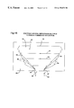
- FIG. 1 illustrates a small rectangular portion 9 of the slab 2 shown in FIG. 4 and which defines waveguides forming a simple two-arm Mach Zehnder filter.
- the portion 9 of FIG. 1 corresponds to a Y junction 10 at which a first waveguide 11 branches into second and third waveguides 12 and 13 .
- the waveguides 12 and 13 are brought into sufficiently close proximity to provide coupling at a 3 db coupler 26 and thereafter diverge.
- the waveguides 12 and 13 define optical path lengths of L and L+dL respectively between the junction 10 and the coupling 26 .
- An input optical fibre 14 is connected to the slab 2 to launch the optical signal 7 into an input region 15 defined by the first waveguide 11 .
- Output optical fibres 16 and 17 are connected to the slab 2 to receive components of the optical signal from output regions 18 and 19 of the slab defined by the second and third waveguides respectively.
- the difference in path length dL between the first and second waveguides 12 and 13 results in there being a modification to the frequency characteristics in an output optical signal 20 as illustrated in FIG. 5 .
- the depth of modulation of signal power as a function of frequency is dependent upon the relative powers input into waveguides 12 and 13 from the Y junction 10 .
- the location of the frequency peaks f x , f y , f z relative to the frequency scale, i.e. the “phase” in frequency space of the modulation, is dependent upon the value of the difference in path length dL, as is the separation between peaks in the envelope of the spectrum.
- the filter provided by the Mach-Zehnder interferometer of FIG. 4 has a fixed frequency characteristic.
- the filter may be made adaptive by modulating transmission in the waveguides of the interferometer as illustrated in the example of FIG. 6 .
- FIG. 6 illustrates a Mach-Zehnder interferometer similar to that of FIG. 4 and will be described using corresponding reference numerals for corresponding elements where appropriate.
- a first modulator 21 is externally controllable to vary the ratio of the input optical signal diverted into each one of the second and third waveguides 12 and 13 .
- FIG. 7 illustrates an example of the manner in which the first modulator 21 may be implemented to vary the proportion of the optical signal diverted into arms of the Y junction 10 .
- the third waveguide 13 is modified by the presence of controllable lattice sites 22 located in the waveguide region in areas 38 and 39 and comprising cylindrical columns formed of a ferrite material to which a variably controllable external field is applied.
- the locations of the controllable lattice sites conform to the column and row positions of the surrounding lattice region and in effect form an extension of the lattice.
- the presence of the controllable lattice sites 22 can therefore in effect be turned on or off in variable number to thereby variably control the effective apertures of the second and third waveguides 12 and 13 .
- the amount of optical signal coupled into the third waveguide is thereby controllable by setting the number of sites which are turned on, the remainder of the optical signal being diverted into the second waveguide 12 .
- Control of the controllable lattice sites 22 is effected such as to vary the dielectric constant of the material forming the cylindrical columns 8 .
- This variation may be continuous or discrete, i.e. variable between one of a number of stepped levels.
- a second modulator 23 is provided for varying the optical path length dL and is shown in greater detail in FIG. 8.
- a dielectric region 24 within the waveguide region defining the third waveguide 13 is subject to an externally applied control to vary the dielectric properties of the region.
- the externally applied control may be one of a number of available options including the application of local heating, the injection of electrical current into the semi-conductor material forming the dielectric, or other suitable optically, electromagnetically or electro-mechanically induced effects.
- the surrounding lattice region is substantially unaffected by this control and continues to serve as a means of confining the optical signal 7 within the waveguide so as to pass through the controlled dielectric region 24 .
- FIG. 9 illustrates in greater detail the construction of the 3 dB coupler 26 .
- the second and third waveguides 12 and 13 are represented in each case by pairs of parallel lines which denote the boundary between the lattice region 3 and the waveguide regions defining the waveguides and which are free of lattice sites.
- the extent of penetration of evanescent wave components of the optical signal in the lattice region 3 are represented as boundaries 40 .
- the evanescent wave components decay exponentially as a function of penetration distance into the lattice region 3 and the indication of boundaries 40 should therefore be regarded only as schematic.
- the boundaries 40 serve to indicate a merging of the region of lattice region 3 within which the evanescent field components of the respective waveguides 12 and 13 penetrate so that a coupling region 41 within the lattice region 3 is defined and serves as a mechanism for phase dependent transfer of energy between modes propagated through the respective waveguides.
- a third modulator 25 in FIG. 6 is used to control the recombining and splitting characteristics of the coupler 26 .
- the third modulator 25 as shown in greater detail in FIG. 10 comprises a portion 27 of the lattice extending into the waveguide region and comprised of controllable lattice sites 28 of the type referred to above with reference to FIG. 7 .
- the amount of optical signal output via the output optical fibre 17 is variably controllable. Light which cannot be transmitted because of the presence of the controlled lattice sites 28 is redirected to emerge from the output optical fibre 16 .
- the frequency characteristics of the filter constituted by the Mach-Zehnder interferometer of FIG. 6 may thereby be variably controlled using any one of, or a combination of, the first, second and third modulators 21 , 23 and 25 .
- a more complex equalizer may be constructed from multiple waveguides as shown for example in FIG. 11 in which waveguides are, for simplicity, represented by single lines, such as waveguides 30 and 31 of substantially equal length which extend between a first star coupler 32 and second star coupler 33 .
- the equalizer of FIG. 11 provides a multiple arm Mach-Zehnder interferometer for frequency response synthesis in which the additive effect of transmission through the arms of the waveguide array is represented in the block representation of FIG. 12 .
- the equalizer transfer function T is synthesized by the effect of a multiple arm Mach-Zehnder interferometer to provide the transfer function shown in FIG. 13 . As represented in FIG.
- a series of delays L, L+dL, L+2dL, L+KdL are provided by delay waveguides 53 to 55 and the contribution made by each delay waveguide to the output combined by a combiner 50 is adaptively controlled by means of a set of modulators 56 where each of one the delays 53 to 55 is provided with a respective modulator.
- phase modulation here implies a variation in optical path length resulting in a corresponding phase variation at the point of combination in combiner 50 .
- the result of the summation of the outputs from the modulated delay waveguides is illustrated schematically in FIG. 13 and has a form which is related to the values of C r by a discrete Fourier transform.
- the values of C r for a required transfer function may be calculated and, in the case of a wavelength division multiplexed optical signal, it is preferable to define the desired transfer function in terms of coefficients T n for N frequencies corresponding in both number and frequency value to the N wavelength channels of the input optical signal to be processed.
- FIG. 12 may be implemented using a photonic crystal provided that the modulators 56 are capable of providing the required amplitude and phase variation.
- the example of FIG. 11 makes use of a simpler form of modulation for which each one of the waveguides of FIG. 13 is replaced by a respective pair of waveguides in the array of FIG. 11 .
- the pair of waveguides 30 and 31 have respective modulators 37 and 36 , each of which has the form of modulator described above with reference to FIG. 8 in which a controlled dielectric region 24 has variable dielectric properties controlled thermally or otherwise.
- This form of control provides adjustment to the optical path length of each of the waveguides in the array of FIG. 12, thereby effectively controlling the phase of each component.
- phase values implemented in the modulators 36 and 37 are selected such that the combined output of these two waveguides has the required amplitude and phase corresponding to the respective one of the complex coupling coefficients C r .
- each one of the waveguides represented in FIG. 12 may be implemented as a respective group of 3 waveguides of equal lengths in the equalizer of FIG. 11, each of the group of waveguides having respective phase control modulators.
- FIG. 14 illustrates the manner in which the equalizer of FIG. 11 may be used to provide equalization for a line amplifier in an optical communications system, as for example where it is necessary to compensate for the effects of gain tilt.
- the optical signal output from the first fibre amplifier 64 is input to the adaptive equalizer 67 , the output of which is input to the second fibre amplifier 65 and amplified before onward transmission in the optical system.
- a second optical tap 70 provides an optical sample of the optical signal output from the equalizer 67 which is detected and measured by a second detector 71 producing measured output channel levels X n .
- the equalizer 67 is adaptive in the sense of being operable to independently control transmission amplitudes of each of the wavelength division multiplexed channels, as represented by transfer function T having complex coefficients T n relating the amplitude and phase of each component output to its respective input.
- These coefficients T n are target values representative of E field values arrived at by calculation and applied by calculating corresponding settings S m of variable components of the equalizer 67 .
- An equalizer controller 72 controls the value of the equalizer settings S m applied to the variable components of the equalizer 67 .
- the number of settings S m may be typically greater than the number N of channels and will depend upon the manner in which the equalizer is implemented. In the example of FIG. 11, each S m is the phase control of one of the waveguides and therefore the number of S m to be calculated is equal to 2 ⁇ N.
- the required values of the equalizer settings S m are determined by calculator 73 to enable a user to input via an input device 76 a referenced spectral characteristic W n which serves as a target value to which output channel levels X n are driven to correspond under ideal operating conditions.
- timing controller 75 which periodically outputs control signals to the first and second detectors to determine the sampling times at which V n and X n are calculated and correspondingly controls the timing at which the settings S m of the equalizer 67 are updated.
- FIG. 14 allows the output to be monitored and its frequency characteristics measured and compared with target settings. This feedback allows a desired frequency characteristic to be achieved iteratively over a number of applications of the values of S m .
- FIG. 15 illustrates an alternative device for providing a number of distinct optical pathways for conducting components of the optical signal between an input region 87 and output region 88 where the number of pathways is greater than two.
- a latticed region 80 of photonic band gap material is formed with a waveguide region 81 which defines a cavity 82 , the term cavity being used here to indicate an enclosed region of the dielectric material of the slab 2 which is free of lattice sites and therefore transmissive to the optical signal.
- a boundary 83 defined by the transition between latticed region 80 and waveguide region 81 is shaped to provide first and second sidewalls 84 and 85 , each having a stepped profile when viewed orthogonally to the plane of the slab 2 .
- the stepped sidewalls 84 and 85 each include a series of concave reflectors 86 , defined by portions of the boundary 83 , which are oriented to reflect components of the optical signal.
- the input region 87 of the waveguide region 81 is coupled to an optical fibre 89 via which the optical signal is input and a further optical fibre 90 is coupled to the output region 88 of the waveguide region.
- the optical signal on entering the input region 87 is spread out in fan formation to illuminate the reflectors 86 of the first sidewall 84 and individual components such as 91 and 92 illustrated in FIG. 15 of the optical signal are separately reflected by respective reflectors 86 and directed onto corresponding reflectors of the second sidewall 85 . Reflection of the components from the sidewall 85 converges the optical signal to be collected and output via the output region 88 and optical fibre 90 .
- Each of the reflectors 86 is concave to direct and concentrate the respective component onto the corresponding reflector of the second sidewall 85 and achieve convergence at the output region 88 .
- the device of FIG. 15 thereby provides for the input signal to be divided into a number of distinct components 91 , 92 which traverse different optical pathlengths before being recombined in the output region 88 .
- the respective path lengths remain constant and the effects of interference in the output region produce a predetermined transfer function, or in other words a set profile of equalization applied to the frequency components of the optical signal.
- FIG. 16 shows an alternative device which is equivalent to the device of FIG. 15 but with the addition of an array 93 of modulators 94 located within the cavity 82 such that each modulating element 94 lies in the path of a respective component 91 of the optical signal.
- Controlled actuation of each of the modulator elements 94 in the array 93 provides means for modifying the transfer function of the device, for example by controlling the amplitude of each of the components.
- the modulator elements 94 may introduce controlled amounts of change in optical pathlength, thereby effectively changing the relative phase of the components before recombination, or alternatively both amplitude and phase may be variably controlled by appropriate modulator elements.
- the modulator elements of FIG. 16 may be controlled in a similar manner to the method of control described above with reference to FIGS. 13 and 14 in order to achieve adaptive equalization.
- the modulator elements 94 may conveniently be formed by providing controlled lattice sites of the type referred to above with reference to FIG. 7 as a means of providing amplitude modulation. Phase modulation may be provided by the external application of thermal or electromagnetic fields to the bulk material forming the slab 2 in the locality of the modulator element 94 .
- FIG. 17 illustrates an alternative device for achieving adaptive equalization of an optical signal and comprises a latticed region 100 formed by a regular array of lattice sites providing a photonic bandgap at optical frequencies including the frequency range of the optical signal.
- waveguides are represented by single lines which are bold to distinguish waveguides from other boundary features.
- a waveguide region formed by the omission of latticed sites is provided with an input region 101 , an output region 102 and a plurality of channels defining waveguides 103 for conducting respective components of the optical signal by respectively different optical path lengths extending between the input and output regions.
- the input region 101 communicates with a first coupling region 104 defined by a fan shaped portion of waveguide region which is free of lattice sites, the first coupling region having a side wall 105 extending linearly and oriented relative to the input region such that the input optical signal is incident upon the sidewall at a shallow angle of grazing incidence.
- a Bloch surface wave thereafter propagates along the sidewall 105 in the manner described for example by Joannopoulous, “Photonic Crystals Moulding the Flow of Light”, Princeton University, 1995, at page 73 to 77.
- Such surface modes in the case of a perfectly formed sidewall 105 of regular lattice sites will guide the optical signal close to the sidewall to enter a waveguide 106 located at the end of the sidewall.
- An array of controlled lattice sites 107 is distributed along the sidewall 105 and includes lattice sites which are selectively activated to perturb the surface wave and cause deflection of components of the optical signal away from the sidewall into the first coupling region 104 so as to enter selectively ones of the waveguides 103 . In this manner, the proportion of the optical signal diverted into each of the waveguides 103 is controlled.
- the outputs of the waveguides 103 communicate with a second coupling region 108 in which the waveguide 106 enters relative to a second sidewall 109 at a shallow angle of grazing incidence, thereby confining the component conducted by waveguide 103 to a surface wave communicating with the output region 102 .
- a further array of controlled lattice sites 110 is provided along the boundary between latticed region 100 and waveguide region at the sidewall 109 to selectively divert a proportion of the optical signal component received from the waveguide 106 .
- the outputs of the remaining waveguides 103 enter the second coupling region 108 and converge on the output region 102 so as to be collected and emerge via an output optical fibre 111 .
- Equalization may thereby be adaptively applied to an optical signal entering the device via input optical fibre 99 and exiting via output optical fibre ill, the control mechanism for determining the control parameters applied to the arrays 107 and 110 of controlled latticed sites corresponding generally to the arrangement described above with reference to FIGS. 13 and 14.
- FIG. 18 shows schematically the propagation of a surface wave 112 parallel to the boundary between lattice region 100 and the coupling region 108 .
- a surface layer 113 of controlled lattice sites 114 allows selected sites to be varied in dielectric properties so as to create discontinuities in the surface layer, thereby achieving selectively a controlled amount of scattering of the optical signals in directions indicated by arrows 115 .
- the amount of light scattered into each of the waveguides 103 may thereby be variably controlled.
- the band gap is formed by a two dimensional array of lattice sites in which the array is of square configuration.
- Other forms of array may be utilised such as a triangular array or honeycomb shaped array.
- the array may be three dimensional.
- multiple waveguides have been disclosed in arrays which have discrete non-overlapping paths. More complex devices are envisaged in which overlapping meshed paths are utilised in order to achieve more complex relationships between division and recombination of components of the optical signal.
- the path lengths described in the above embodiments include linearly increasing length differentials, i.e. multiples of dL. More generally, embodiments are envisaged in which non-linear progressions of path lengths are utilised, such as chirped systems where the differential lengths follow a squared, cubic or exponential progression. Gapped or staggered sequences of increasing path length may also be utilised.
- the input region and output region are physically separated. It is however envisaged that devices and methods in accordance with the present invention may utilise input and output of optical signals from the same region, as in the case of a Michelson interferometer configuration, and in such instances it is intended that the terms input region and output region may simultaneously apply to the same region.
- optical signals may be reversed, or simultaneously propagated in opposite directions, so that the terms input and output are interchangeable in this context.
Abstract
Description
Claims (20)
Priority Applications (1)
| Application Number | Priority Date | Filing Date | Title |
|---|---|---|---|
| US09/165,053 US6175671B1 (en) | 1998-10-01 | 1998-10-01 | Photonic crystal waveguide arrays |
Applications Claiming Priority (1)
| Application Number | Priority Date | Filing Date | Title |
|---|---|---|---|
| US09/165,053 US6175671B1 (en) | 1998-10-01 | 1998-10-01 | Photonic crystal waveguide arrays |
Publications (1)
| Publication Number | Publication Date |
|---|---|
| US6175671B1 true US6175671B1 (en) | 2001-01-16 |
Family
ID=22597227
Family Applications (1)
| Application Number | Title | Priority Date | Filing Date |
|---|---|---|---|
| US09/165,053 Expired - Lifetime US6175671B1 (en) | 1998-10-01 | 1998-10-01 | Photonic crystal waveguide arrays |
Country Status (1)
| Country | Link |
|---|---|
| US (1) | US6175671B1 (en) |
Cited By (77)
| Publication number | Priority date | Publication date | Assignee | Title |
|---|---|---|---|---|
| US6310991B1 (en) * | 1997-05-17 | 2001-10-30 | Deutsche Telekom Ag | Integrated optical circuit |
| WO2002014914A1 (en) * | 2000-08-15 | 2002-02-21 | Corning Incorporated | Active photonic crystal waveguide device and method |
| WO2002014913A1 (en) * | 2000-08-15 | 2002-02-21 | Corning Incorporated | Active photonic crystal waveguide device |
| US20020060847A1 (en) * | 1998-02-19 | 2002-05-23 | Joannopoulos John D. | High omnidirectional reflector |
| US6411417B1 (en) * | 1998-09-22 | 2002-06-25 | Nortel Networks Limited | Optical equalizer |
| WO2002059656A2 (en) * | 2001-01-25 | 2002-08-01 | Omniguide Communications | Low-loss photonic crystal waveguide having large core radius |
| US20020105000A1 (en) * | 2000-12-20 | 2002-08-08 | Kyocera Corporation | Optical waveguide and optical circuit base component |
| US20020109908A1 (en) * | 2001-02-12 | 2002-08-15 | Koteles Emil S. | Optical dynamic gain amplifier |
| US20020131702A1 (en) * | 2001-03-15 | 2002-09-19 | Morey William W. | Combined multiplexer and demultiplexer for optical communication systems |
| US20020131712A1 (en) * | 2001-03-15 | 2002-09-19 | Markwardt Terry L. | Dynamic variable optical attenuator and variable optical tap |
| US20020131692A1 (en) * | 2001-03-15 | 2002-09-19 | Chen Ray T. | Miniaturized reconfigurable DWDM add/drop system for optical communication system |
| US6456244B1 (en) | 2001-07-23 | 2002-09-24 | Harris Corporation | Phased array antenna using aperiodic lattice formed of aperiodic subarray lattices |
| WO2002082134A1 (en) * | 2001-04-05 | 2002-10-17 | Galian Photonics Inc. | Photonic input/output port |
| US6468823B1 (en) * | 1999-09-30 | 2002-10-22 | California Institute Of Technology | Fabrication of optical devices based on two dimensional photonic crystal structures and apparatus made thereby |
| US20020159698A1 (en) * | 2001-04-30 | 2002-10-31 | Wenhua Lin | Tunable filter |
| WO2002086565A1 (en) * | 2001-04-20 | 2002-10-31 | Bookham Technology Plc | Photonic band gap device |
| US20020167984A1 (en) * | 2001-01-11 | 2002-11-14 | Axel Scherer | Compact electrically and optically pumped multi-wavelength nanocavity laser, modulator and detector arrays and method of making the same |
| WO2002093248A1 (en) * | 2001-05-15 | 2002-11-21 | Massachussets Institute Of Technology | Mach-zehnder interferometer using photonic band gap crystals |
| US20020176676A1 (en) * | 2001-01-25 | 2002-11-28 | Johnson Steven G. | Photonic crystal optical waveguides having tailored dispersion profiles |
| US20030044159A1 (en) * | 2001-04-12 | 2003-03-06 | Emilia Anderson | High index-contrast fiber waveguides and applications |
| US20030048993A1 (en) * | 2001-09-05 | 2003-03-13 | Shouyuan Shi | System for efficient coupling to photonic crystal waveguides |
| US6542654B1 (en) | 2001-07-10 | 2003-04-01 | Optical Switch Corporation | Reconfigurable optical switch and method |
| US20030063885A1 (en) * | 2001-09-10 | 2003-04-03 | Gunn Lawrence Cary | Electronically biased strip loaded waveguide |
| US20030068132A1 (en) * | 2001-09-10 | 2003-04-10 | Gunn Lawrence Cary | Tunable resonant cavity based on the field effect in semiconductors |
| US20030068152A1 (en) * | 2001-09-10 | 2003-04-10 | Gunn Lawrence Cary | Structure and method for coupling light between dissimilar waveguides |
| US20030076274A1 (en) * | 2001-07-23 | 2003-04-24 | Phelan Harry Richard | Antenna arrays formed of spiral sub-array lattices |
| US6560006B2 (en) * | 2001-04-30 | 2003-05-06 | Agilent Technologies, Inc. | Two-dimensional photonic crystal slab waveguide |
| US6563981B2 (en) | 2001-01-31 | 2003-05-13 | Omniguide Communications | Electromagnetic mode conversion in photonic crystal multimode waveguides |
| EP1326132A2 (en) * | 2002-01-08 | 2003-07-09 | Alps Electric Co., Ltd. | Photonic crystal device |
| US20030133661A1 (en) * | 2002-01-16 | 2003-07-17 | Ali Adibi | Use of tapered dielectric slab waveguides for input and output coupling of light into photonic crystal devices |
| US6600597B2 (en) | 2001-03-19 | 2003-07-29 | Jds Uniphase Corporation | Photonic crystal amplifier for optical telecommunications system |
| US6603911B2 (en) | 1998-10-14 | 2003-08-05 | Massachusetts Institute Of Technology | Omnidirectional multilayer device for enhanced optical waveguiding |
| US20030174940A1 (en) * | 1997-05-16 | 2003-09-18 | Btg International Limited | Optical devices and methods of fabrication thereof |
| US6631236B2 (en) * | 2000-03-29 | 2003-10-07 | Nec Corporation | Photonic crystal waveguide and directional coupler using the same |
| US6643439B2 (en) * | 2000-12-27 | 2003-11-04 | Nippon Telegraph And Telephone Corporation | Photonic crystal waveguide |
| WO2003098273A2 (en) * | 2002-05-17 | 2003-11-27 | Mesophotonics Limited | Photonic crystal device |
| US20030228096A1 (en) * | 1997-05-16 | 2003-12-11 | Mesophotonics Limited | Optical delay device |
| WO2004003611A1 (en) * | 2002-06-28 | 2004-01-08 | Australian Photonics Pty Ltd | Writing of photo-induced structures |
| US20040008437A1 (en) * | 2002-05-17 | 2004-01-15 | Shigeo Kittaka | Optical element using one-dimensional photonic crystal and spectroscopic device using the same |
| US6684008B2 (en) | 2000-09-01 | 2004-01-27 | The University Of British Columbia | Planar photonic bandgap structures for controlling radiation loss |
| US6687447B2 (en) * | 2001-04-30 | 2004-02-03 | Agilent Technologies, Inc. | Stub-tuned photonic crystal waveguide |
| US6690325B1 (en) * | 2002-06-21 | 2004-02-10 | The United States Of America As Represented By The Secretary Of The Army | Method and apparatus for generating true time delays |
| EP1388962A2 (en) * | 2002-08-09 | 2004-02-11 | Samsung Electronics Co., Ltd. | Polarization mode dispersion compensation apparatus using a photonic crystal structure |
| US6708003B1 (en) * | 1999-12-16 | 2004-03-16 | Northrop Grumman Corporation | Optical energy transmission system utilizing precise phase and amplitude control |
| US20040120639A1 (en) * | 2000-08-21 | 2004-06-24 | Jorg-Pete Elbers | Method and device for determining and compensating for the tilting of the spectrum in an optical fiber of a data transmission path |
| US20040137168A1 (en) * | 2002-11-22 | 2004-07-15 | Vladimir Fuflyigin | Dielectric waveguide and method of making the same |
| US20040141459A1 (en) * | 2003-01-21 | 2004-07-22 | Tinker Frank A. | Analog implementation of linear transforms |
| EP1460461A2 (en) * | 2003-03-17 | 2004-09-22 | President, Kyoto University | Channel add/drop filter and channel monitor employing two-dimensional photonic crystal |
| US20040240784A1 (en) * | 2003-05-30 | 2004-12-02 | General Electric Company | Apparatus for coupling electromagnetic energy and method of making |
| US20050001784A1 (en) * | 2001-07-23 | 2005-01-06 | Harris Corporation | Phased array antenna providing gradual changes in beam steering and beam reconfiguration and related methods |
| US6853760B2 (en) * | 2000-01-24 | 2005-02-08 | Minolta Co., Ltd. | Optical functional device and optical integrated device |
| US20050249455A1 (en) * | 2001-04-04 | 2005-11-10 | Nec Corporation | Optical switch having photonic crystal structure |
| US20060066866A1 (en) * | 2004-09-27 | 2006-03-30 | Shih-Yuan Wang | Mach Zehnder photonic crystal sensors and methods |
| US20060126992A1 (en) * | 2002-12-26 | 2006-06-15 | Toshikazu Hashimoto | Wave transmission medium and waveguide circuit |
| US20060233504A1 (en) * | 2004-06-07 | 2006-10-19 | Hochberg Michael J | Segmented waveguide structures |
| US20070047887A1 (en) * | 2005-08-30 | 2007-03-01 | Uni-Pixel Displays, Inc. | Reducing light leakage and improving contrast ratio performance in FTIR display devices |
| US20080112669A1 (en) * | 2006-11-09 | 2008-05-15 | Electronics And Telecommunications Research Institute | Two-dimensional Planar photonic crystal superprism device and method of manufacturing the same |
| US7389019B1 (en) * | 2006-12-19 | 2008-06-17 | Verizon Services Organization Inc. | Variable photonic coupler |
| US20080166083A1 (en) * | 2007-01-08 | 2008-07-10 | Christopher Richard Doerr | Compact optical modulator |
| WO2008113176A1 (en) * | 2007-03-22 | 2008-09-25 | National Research Council Of Canada | Planar waveguide wavelength dispersive devices with multiple waveguide input aperture |
| CN100437210C (en) * | 2002-06-27 | 2008-11-26 | 皇家飞利浦电子股份有限公司 | Electrically configurable photonic crystal |
| EP1999511A2 (en) * | 2006-03-17 | 2008-12-10 | Searete LLC. | Photonic crystal surface states |
| US20090196561A1 (en) * | 2006-03-17 | 2009-08-06 | Searete Llc, A Limited Liability Corporation Of The State Of Delaware | Photonic crystal surface states |
| US20090245811A1 (en) * | 2008-03-28 | 2009-10-01 | Hill Randy W | High bandwidth communication system and method |
| WO2010099104A2 (en) * | 2009-02-24 | 2010-09-02 | Aidi Corporation | Planar lightwave fourier-transform spectrometer |
| US7826688B1 (en) | 2005-10-21 | 2010-11-02 | Luxtera, Inc. | Enhancing the sensitivity of resonant optical modulating and switching devices |
| US20110194120A1 (en) * | 2009-05-21 | 2011-08-11 | Monash University | Method and device for phase measurement |
| US8406580B2 (en) | 2010-07-28 | 2013-03-26 | Aidi Corporation | Planar lightwave fourier-transform spectrometer measurement including phase shifting for error correction |
| CN106370302A (en) * | 2016-09-29 | 2017-02-01 | 浙江大学 | Space-time joint modulation and MZI optical waveguide array-based imaging spectrometer |
| CN109038211A (en) * | 2018-08-14 | 2018-12-18 | 华中科技大学 | A kind of laser light source based on acousto-optic interaction |
| USD840404S1 (en) | 2013-03-13 | 2019-02-12 | Nagrastar, Llc | Smart card interface |
| US10382816B2 (en) | 2013-03-13 | 2019-08-13 | Nagrastar, Llc | Systems and methods for performing transport I/O |
| USD864968S1 (en) | 2015-04-30 | 2019-10-29 | Echostar Technologies L.L.C. | Smart card interface |
| US20200025616A1 (en) * | 2016-09-26 | 2020-01-23 | Ixa Amc Office / Academic Medical Center | High-resolution integrated-optics-based spectrometer |
| US10907951B2 (en) | 2016-09-26 | 2021-02-02 | Academisch Medisch Centrum | Single-chip optical coherence tomography device |
| US20220196384A1 (en) * | 2020-12-21 | 2022-06-23 | Commissariat A L'energie Atomique Et Aux Energies Alternatives | Optical component for an atr interferometric imaging device |
| EP4286935A3 (en) * | 2018-04-11 | 2024-03-13 | Microsoft Technology Licensing, LLC | Optical waveguiding structure comprising a photonic crystal nanostructure |
Citations (11)
| Publication number | Priority date | Publication date | Assignee | Title |
|---|---|---|---|---|
| US4786130A (en) * | 1985-05-29 | 1988-11-22 | The General Electric Company, P.L.C. | Fibre optic coupler |
| US5389943A (en) | 1991-02-15 | 1995-02-14 | Lockheed Sanders, Inc. | Filter utilizing a frequency selective non-conductive dielectric structure |
| US5418868A (en) * | 1993-11-17 | 1995-05-23 | At&T Corp. | Thermally activated optical switch |
| US5513029A (en) | 1994-06-16 | 1996-04-30 | Northern Telecom Limited | Method and apparatus for monitoring performance of optical transmission systems |
| US5526449A (en) * | 1993-01-08 | 1996-06-11 | Massachusetts Institute Of Technology | Optoelectronic integrated circuits and method of fabricating and reducing losses using same |
| US5651818A (en) | 1992-12-04 | 1997-07-29 | Milstein; Joseph B. | Photonic band gap materials and method of preparation thereof |
| US5684817A (en) * | 1995-05-12 | 1997-11-04 | Thomson-Csf | Semiconductor laser having a structure of photonic bandgap material |
| US5748057A (en) * | 1996-06-03 | 1998-05-05 | Hughes Electronics | Photonic bandgap crystal frequency multiplexers and a pulse blanking filter for use therewith |
| US5784400A (en) | 1995-02-28 | 1998-07-21 | Massachusetts Institute Of Technology | Resonant cavities employing two dimensionally periodic dielectric materials |
| US5973823A (en) * | 1997-07-22 | 1999-10-26 | Deutsche Telekom Ag | Method for the mechanical stabilization and for tuning a filter having a photonic crystal structure |
| US6016374A (en) * | 1997-11-04 | 2000-01-18 | Lucent Technologies Inc. | Optical fiber communications system with adaptive data equalizer |
-
1998
- 1998-10-01 US US09/165,053 patent/US6175671B1/en not_active Expired - Lifetime
Patent Citations (11)
| Publication number | Priority date | Publication date | Assignee | Title |
|---|---|---|---|---|
| US4786130A (en) * | 1985-05-29 | 1988-11-22 | The General Electric Company, P.L.C. | Fibre optic coupler |
| US5389943A (en) | 1991-02-15 | 1995-02-14 | Lockheed Sanders, Inc. | Filter utilizing a frequency selective non-conductive dielectric structure |
| US5651818A (en) | 1992-12-04 | 1997-07-29 | Milstein; Joseph B. | Photonic band gap materials and method of preparation thereof |
| US5526449A (en) * | 1993-01-08 | 1996-06-11 | Massachusetts Institute Of Technology | Optoelectronic integrated circuits and method of fabricating and reducing losses using same |
| US5418868A (en) * | 1993-11-17 | 1995-05-23 | At&T Corp. | Thermally activated optical switch |
| US5513029A (en) | 1994-06-16 | 1996-04-30 | Northern Telecom Limited | Method and apparatus for monitoring performance of optical transmission systems |
| US5784400A (en) | 1995-02-28 | 1998-07-21 | Massachusetts Institute Of Technology | Resonant cavities employing two dimensionally periodic dielectric materials |
| US5684817A (en) * | 1995-05-12 | 1997-11-04 | Thomson-Csf | Semiconductor laser having a structure of photonic bandgap material |
| US5748057A (en) * | 1996-06-03 | 1998-05-05 | Hughes Electronics | Photonic bandgap crystal frequency multiplexers and a pulse blanking filter for use therewith |
| US5973823A (en) * | 1997-07-22 | 1999-10-26 | Deutsche Telekom Ag | Method for the mechanical stabilization and for tuning a filter having a photonic crystal structure |
| US6016374A (en) * | 1997-11-04 | 2000-01-18 | Lucent Technologies Inc. | Optical fiber communications system with adaptive data equalizer |
Non-Patent Citations (3)
| Title |
|---|
| Dragone, IEEE Photon. Technology Letters, Sep. 1991, pp. 812 to 815. |
| H. Kosaka et al., "Superprism Phenomena in Photonic Crystals: Toward Microscale Lightwave Circuits," J. Lightwave Technology, vol. 17, No. 11, pp. 2032-2038, Nov. 1999. * |
| Joannopoulos et al, Photonic Crystals, Molding the Flow of Light, Chapter 5, "Two-Dimensional Photonic Crystals", 1995 (No Month). |
Cited By (178)
| Publication number | Priority date | Publication date | Assignee | Title |
|---|---|---|---|---|
| US6640034B1 (en) | 1997-05-16 | 2003-10-28 | Btg International Limited | Optical photonic band gap devices and methods of fabrication thereof |
| US20040156610A1 (en) * | 1997-05-16 | 2004-08-12 | Btg International Limited | Optical devices and methods of fabrication thereof |
| US6901194B2 (en) | 1997-05-16 | 2005-05-31 | Btg International Limited | Optical devices and methods of fabrication thereof |
| US6788863B2 (en) | 1997-05-16 | 2004-09-07 | Mesophotonics Limited | Optical delay device |
| US20030228096A1 (en) * | 1997-05-16 | 2003-12-11 | Mesophotonics Limited | Optical delay device |
| US6778746B2 (en) | 1997-05-16 | 2004-08-17 | Btg International Limited | Optical devices and methods of fabrication thereof |
| US20030174940A1 (en) * | 1997-05-16 | 2003-09-18 | Btg International Limited | Optical devices and methods of fabrication thereof |
| US6735368B2 (en) | 1997-05-16 | 2004-05-11 | Mesophotonics Limited | Optical delay device |
| US6310991B1 (en) * | 1997-05-17 | 2001-10-30 | Deutsche Telekom Ag | Integrated optical circuit |
| US6903873B1 (en) | 1998-02-19 | 2005-06-07 | Omniguide Communications | High omnidirectional reflector |
| US20020060847A1 (en) * | 1998-02-19 | 2002-05-23 | Joannopoulos John D. | High omnidirectional reflector |
| US6411417B1 (en) * | 1998-09-22 | 2002-06-25 | Nortel Networks Limited | Optical equalizer |
| US6603911B2 (en) | 1998-10-14 | 2003-08-05 | Massachusetts Institute Of Technology | Omnidirectional multilayer device for enhanced optical waveguiding |
| US6468823B1 (en) * | 1999-09-30 | 2002-10-22 | California Institute Of Technology | Fabrication of optical devices based on two dimensional photonic crystal structures and apparatus made thereby |
| US6708003B1 (en) * | 1999-12-16 | 2004-03-16 | Northrop Grumman Corporation | Optical energy transmission system utilizing precise phase and amplitude control |
| US6853760B2 (en) * | 2000-01-24 | 2005-02-08 | Minolta Co., Ltd. | Optical functional device and optical integrated device |
| US6631236B2 (en) * | 2000-03-29 | 2003-10-07 | Nec Corporation | Photonic crystal waveguide and directional coupler using the same |
| US6674949B2 (en) | 2000-08-15 | 2004-01-06 | Corning Incorporated | Active photonic crystal waveguide device and method |
| WO2002014914A1 (en) * | 2000-08-15 | 2002-02-21 | Corning Incorporated | Active photonic crystal waveguide device and method |
| WO2002014913A1 (en) * | 2000-08-15 | 2002-02-21 | Corning Incorporated | Active photonic crystal waveguide device |
| US6542682B2 (en) | 2000-08-15 | 2003-04-01 | Corning Incorporated | Active photonic crystal waveguide device |
| US7197210B2 (en) * | 2000-08-21 | 2007-03-27 | Siemens Aktiengesellschaft | Method and device for determining and compensating for the tilting of the spectrum in an optical fiber of a data transmission path |
| US20040120639A1 (en) * | 2000-08-21 | 2004-06-24 | Jorg-Pete Elbers | Method and device for determining and compensating for the tilting of the spectrum in an optical fiber of a data transmission path |
| US6684008B2 (en) | 2000-09-01 | 2004-01-27 | The University Of British Columbia | Planar photonic bandgap structures for controlling radiation loss |
| US6785454B2 (en) * | 2000-12-20 | 2004-08-31 | Kyocera Corporation | Optical waveguide and optical circuit base component |
| US20020105000A1 (en) * | 2000-12-20 | 2002-08-08 | Kyocera Corporation | Optical waveguide and optical circuit base component |
| US6643439B2 (en) * | 2000-12-27 | 2003-11-04 | Nippon Telegraph And Telephone Corporation | Photonic crystal waveguide |
| US6804283B2 (en) * | 2001-01-11 | 2004-10-12 | California Institute Of Technology | Compact electrically and optically pumped multi-wavelength nanocavity laser, modulator and detector arrays and method of making the same |
| US20020167984A1 (en) * | 2001-01-11 | 2002-11-14 | Axel Scherer | Compact electrically and optically pumped multi-wavelength nanocavity laser, modulator and detector arrays and method of making the same |
| US6895154B2 (en) | 2001-01-25 | 2005-05-17 | Omniguide Communications | Photonic crystal optical waveguides having tailored dispersion profiles |
| US20020176676A1 (en) * | 2001-01-25 | 2002-11-28 | Johnson Steven G. | Photonic crystal optical waveguides having tailored dispersion profiles |
| WO2002059656A2 (en) * | 2001-01-25 | 2002-08-01 | Omniguide Communications | Low-loss photonic crystal waveguide having large core radius |
| WO2002059656A3 (en) * | 2001-01-25 | 2002-09-19 | Omniguide Comm | Low-loss photonic crystal waveguide having large core radius |
| AU2002240145B2 (en) * | 2001-01-25 | 2006-06-29 | Omniguide, Inc. | Low-loss photonic crystal waveguide having large core radius |
| US7072553B2 (en) | 2001-01-25 | 2006-07-04 | Omniguide Communications | Low-loss photonic crystal waveguide having large core radius |
| US6625364B2 (en) | 2001-01-25 | 2003-09-23 | Omniguide Communications | Low-loss photonic crystal waveguide having large core radius |
| US20040013379A1 (en) * | 2001-01-25 | 2004-01-22 | Omniguide Communications, A Delaware Corporation | Low-loss photonic crystal waveguide having large core radius |
| US6728439B2 (en) | 2001-01-31 | 2004-04-27 | Omniguide Communications | Electromagnetic mode conversion in photonic crystal multimode waveguides |
| US6563981B2 (en) | 2001-01-31 | 2003-05-13 | Omniguide Communications | Electromagnetic mode conversion in photonic crystal multimode waveguides |
| US20020109908A1 (en) * | 2001-02-12 | 2002-08-15 | Koteles Emil S. | Optical dynamic gain amplifier |
| US7019893B2 (en) | 2001-02-12 | 2006-03-28 | Metrophotonics Inc. | Optical dynamic gain amplifier |
| US7103244B2 (en) | 2001-03-15 | 2006-09-05 | Finisar Corporation | Miniaturized reconfigurable DWDM add/drop system for optical communication system |
| US7006727B2 (en) | 2001-03-15 | 2006-02-28 | Fluisar Corporation | Combined multiplexer and demultiplexer for optical communication systems |
| US6778736B2 (en) | 2001-03-15 | 2004-08-17 | Finisar Corporation | Dynamic variable optical attenuator and variable optical tap |
| US20020131692A1 (en) * | 2001-03-15 | 2002-09-19 | Chen Ray T. | Miniaturized reconfigurable DWDM add/drop system for optical communication system |
| US20020131712A1 (en) * | 2001-03-15 | 2002-09-19 | Markwardt Terry L. | Dynamic variable optical attenuator and variable optical tap |
| US20020131702A1 (en) * | 2001-03-15 | 2002-09-19 | Morey William W. | Combined multiplexer and demultiplexer for optical communication systems |
| US7024085B2 (en) * | 2001-03-15 | 2006-04-04 | Finisar Corporation | Systems and devices for dynamic processing of optical signals |
| US20040218855A1 (en) * | 2001-03-15 | 2004-11-04 | Markwardt Terry L. | Systems and devices for dynamic processing of optical signals |
| US6600597B2 (en) | 2001-03-19 | 2003-07-29 | Jds Uniphase Corporation | Photonic crystal amplifier for optical telecommunications system |
| US20050249455A1 (en) * | 2001-04-04 | 2005-11-10 | Nec Corporation | Optical switch having photonic crystal structure |
| US7263251B2 (en) * | 2001-04-04 | 2007-08-28 | Nec Corporation | Optical switch having photonic crystal structure |
| US6788847B2 (en) | 2001-04-05 | 2004-09-07 | Luxtera, Inc. | Photonic input/output port |
| WO2002082134A1 (en) * | 2001-04-05 | 2002-10-17 | Galian Photonics Inc. | Photonic input/output port |
| US20020164118A1 (en) * | 2001-04-05 | 2002-11-07 | Paddon Paul J. | Photonic input/output port |
| US20030049003A1 (en) * | 2001-04-12 | 2003-03-13 | Ahmad Rokan U. | High index-contrast fiber waveguides and applications |
| US6788864B2 (en) | 2001-04-12 | 2004-09-07 | Omniguide Communications | High index-contrast fiber waveguides and applications |
| US20030044159A1 (en) * | 2001-04-12 | 2003-03-06 | Emilia Anderson | High index-contrast fiber waveguides and applications |
| US7142756B2 (en) | 2001-04-12 | 2006-11-28 | Omniguide, Inc. | High index-contrast fiber waveguides and applications |
| US7190875B2 (en) | 2001-04-12 | 2007-03-13 | Omniguide, Inc. | Fiber waveguide formed from chalcogenide glass and polymer |
| US6801698B2 (en) | 2001-04-12 | 2004-10-05 | Omniguide Communications | High index-contrast fiber waveguides and applications |
| US20050259944A1 (en) * | 2001-04-12 | 2005-11-24 | Emilia Anderson | High index-contrast fiber waveguides and applications |
| US6898359B2 (en) | 2001-04-12 | 2005-05-24 | Omniguide Communications | High index-contrast fiber waveguides and applications |
| WO2002086565A1 (en) * | 2001-04-20 | 2002-10-31 | Bookham Technology Plc | Photonic band gap device |
| US6853773B2 (en) * | 2001-04-30 | 2005-02-08 | Kotusa, Inc. | Tunable filter |
| US6687447B2 (en) * | 2001-04-30 | 2004-02-03 | Agilent Technologies, Inc. | Stub-tuned photonic crystal waveguide |
| US6560006B2 (en) * | 2001-04-30 | 2003-05-06 | Agilent Technologies, Inc. | Two-dimensional photonic crystal slab waveguide |
| US20020159698A1 (en) * | 2001-04-30 | 2002-10-31 | Wenhua Lin | Tunable filter |
| US6917431B2 (en) | 2001-05-15 | 2005-07-12 | Massachusetts Institute Of Technology | Mach-Zehnder interferometer using photonic band gap crystals |
| US20030011775A1 (en) * | 2001-05-15 | 2003-01-16 | Marin Soljacic | Mach-Zehnder interferometer using photonic band gap crystals |
| WO2002093248A1 (en) * | 2001-05-15 | 2002-11-21 | Massachussets Institute Of Technology | Mach-zehnder interferometer using photonic band gap crystals |
| US6542654B1 (en) | 2001-07-10 | 2003-04-01 | Optical Switch Corporation | Reconfigurable optical switch and method |
| US20050001784A1 (en) * | 2001-07-23 | 2005-01-06 | Harris Corporation | Phased array antenna providing gradual changes in beam steering and beam reconfiguration and related methods |
| US20030076274A1 (en) * | 2001-07-23 | 2003-04-24 | Phelan Harry Richard | Antenna arrays formed of spiral sub-array lattices |
| US6456244B1 (en) | 2001-07-23 | 2002-09-24 | Harris Corporation | Phased array antenna using aperiodic lattice formed of aperiodic subarray lattices |
| US6897829B2 (en) | 2001-07-23 | 2005-05-24 | Harris Corporation | Phased array antenna providing gradual changes in beam steering and beam reconfiguration and related methods |
| US6842157B2 (en) | 2001-07-23 | 2005-01-11 | Harris Corporation | Antenna arrays formed of spiral sub-array lattices |
| US6782169B2 (en) | 2001-09-05 | 2004-08-24 | University Of Delaware | System for efficient coupling to photonic crystal waveguides |
| US20030048993A1 (en) * | 2001-09-05 | 2003-03-13 | Shouyuan Shi | System for efficient coupling to photonic crystal waveguides |
| US7082235B2 (en) | 2001-09-10 | 2006-07-25 | California Institute Of Technology | Structure and method for coupling light between dissimilar waveguides |
| US6917727B2 (en) | 2001-09-10 | 2005-07-12 | California Institute Of Technology | Strip loaded waveguide integrated with electronics components |
| US20030063885A1 (en) * | 2001-09-10 | 2003-04-03 | Gunn Lawrence Cary | Electronically biased strip loaded waveguide |
| US20070196049A1 (en) * | 2001-09-10 | 2007-08-23 | Gunn Lawrence C Iii | Tunable resonant cavity based on the field effect in semiconductors |
| US6834152B2 (en) | 2001-09-10 | 2004-12-21 | California Institute Of Technology | Strip loaded waveguide with low-index transition layer |
| US6839488B2 (en) | 2001-09-10 | 2005-01-04 | California Institute Of Technology | Tunable resonant cavity based on the field effect in semiconductors |
| US20040202422A1 (en) * | 2001-09-10 | 2004-10-14 | Gunn Lawrence Cary | Tuning the index of a waveguide structure |
| US7120338B2 (en) | 2001-09-10 | 2006-10-10 | California Institute Of Technology | Tuning the index of a waveguide structure |
| US20030068132A1 (en) * | 2001-09-10 | 2003-04-10 | Gunn Lawrence Cary | Tunable resonant cavity based on the field effect in semiconductors |
| US7127147B2 (en) | 2001-09-10 | 2006-10-24 | California Institute Of Technology | Strip loaded waveguide with low-index transition layer |
| US20050089294A1 (en) * | 2001-09-10 | 2005-04-28 | Gunn Lawrence C.Iii | Strip loaded waveguide with low-index transition layer |
| US20050094918A1 (en) * | 2001-09-10 | 2005-05-05 | Gunn Lawrence C.Iii | Tunable resonant cavity based on the field effect in semiconductors |
| US20030068131A1 (en) * | 2001-09-10 | 2003-04-10 | Gunn Lawrence C. | Modulator based on tunable resonant cavity |
| US6895148B2 (en) | 2001-09-10 | 2005-05-17 | California Institute Of Technology | Modulator based on tunable resonant cavity |
| US20030068151A1 (en) * | 2001-09-10 | 2003-04-10 | Gunn Lawrence Cary | Strip loaded waveguide integrated with electronics components |
| US6990257B2 (en) | 2001-09-10 | 2006-01-24 | California Institute Of Technology | Electronically biased strip loaded waveguide |
| US20030068134A1 (en) * | 2001-09-10 | 2003-04-10 | Gunn Lawrence Cary | Tuning the index of a waveguide structure |
| US7203403B2 (en) | 2001-09-10 | 2007-04-10 | California Institute Of Technology | Modulator based on tunable resonant cavity |
| US20050123259A1 (en) * | 2001-09-10 | 2005-06-09 | Gunn Lawrence C.Iii | Strip loaded waveguide integrated with electronics components |
| US20030068152A1 (en) * | 2001-09-10 | 2003-04-10 | Gunn Lawrence Cary | Structure and method for coupling light between dissimilar waveguides |
| US7164821B2 (en) | 2001-09-10 | 2007-01-16 | California Institute Of Technology | Tunable resonant cavity based on the field effect in semiconductors |
| US7167606B2 (en) | 2001-09-10 | 2007-01-23 | California Institute Of Technology | Electronically biased strip loaded waveguide |
| US20050175270A1 (en) * | 2001-09-10 | 2005-08-11 | Gunn Lawrence C.Iii | Electronically biased strip loaded waveguide |
| US20050175274A1 (en) * | 2001-09-10 | 2005-08-11 | Gunn Lawrence C.Iii | Modulator based on tunable resonant cavity |
| US20030128949A1 (en) * | 2002-01-08 | 2003-07-10 | Alps Electric Co., Ltd. | Photonic crystal device having variable bandgap, optical waveguide using the same, and optical multiplexing/demultiplexing device using the same |
| US6931191B2 (en) * | 2002-01-08 | 2005-08-16 | Alps Electric Co., Ltd. | Photonic crystal device having variable bandgap, optical waveguide using the same, and optical multiplexing/demultiplexing device using the same |
| EP1326132A3 (en) * | 2002-01-08 | 2004-09-29 | Alps Electric Co., Ltd. | Photonic crystal device |
| EP1326132A2 (en) * | 2002-01-08 | 2003-07-09 | Alps Electric Co., Ltd. | Photonic crystal device |
| WO2003067291A1 (en) * | 2002-01-16 | 2003-08-14 | California Institute Of Technology | Dielectric slab waveguides for input and output coupling |
| US20030133661A1 (en) * | 2002-01-16 | 2003-07-17 | Ali Adibi | Use of tapered dielectric slab waveguides for input and output coupling of light into photonic crystal devices |
| WO2003098273A3 (en) * | 2002-05-17 | 2004-03-11 | Mesophotonics Ltd | Photonic crystal device |
| US20040008437A1 (en) * | 2002-05-17 | 2004-01-15 | Shigeo Kittaka | Optical element using one-dimensional photonic crystal and spectroscopic device using the same |
| US7068903B2 (en) * | 2002-05-17 | 2006-06-27 | Nippon Sheet Glass Co., Ltd. | Optical element using one-dimensional photonic crystal and spectroscopic device using the same |
| WO2003098273A2 (en) * | 2002-05-17 | 2003-11-27 | Mesophotonics Limited | Photonic crystal device |
| US6690325B1 (en) * | 2002-06-21 | 2004-02-10 | The United States Of America As Represented By The Secretary Of The Army | Method and apparatus for generating true time delays |
| CN100437210C (en) * | 2002-06-27 | 2008-11-26 | 皇家飞利浦电子股份有限公司 | Electrically configurable photonic crystal |
| WO2004003611A1 (en) * | 2002-06-28 | 2004-01-08 | Australian Photonics Pty Ltd | Writing of photo-induced structures |
| US20060125913A1 (en) * | 2002-06-28 | 2006-06-15 | Mark Sceats | Writing of photo-induced structures |
| US20040114937A1 (en) * | 2002-08-09 | 2004-06-17 | Samsung Electronics Co., Ltd. | Polarization mode dispersion compensation apparatus using a photonic crystal structure |
| EP1388962A2 (en) * | 2002-08-09 | 2004-02-11 | Samsung Electronics Co., Ltd. | Polarization mode dispersion compensation apparatus using a photonic crystal structure |
| EP1388962A3 (en) * | 2002-08-09 | 2005-07-13 | Samsung Electronics Co., Ltd. | Polarization mode dispersion compensation apparatus using a photonic crystal structure |
| US7206513B2 (en) | 2002-08-09 | 2007-04-17 | Samsung Electronics Co., Ltd. | Polarization mode dispersion compensation apparatus using a photonic crystal structure |
| US20040137168A1 (en) * | 2002-11-22 | 2004-07-15 | Vladimir Fuflyigin | Dielectric waveguide and method of making the same |
| US20040141702A1 (en) * | 2002-11-22 | 2004-07-22 | Vladimir Fuflyigin | Dielectric waveguide and method of making the same |
| US20080141724A1 (en) * | 2002-11-22 | 2008-06-19 | Omniguide, Inc. | Dielectric waveguide and method of making the same |
| US7854149B2 (en) | 2002-11-22 | 2010-12-21 | Omniguide, Inc. | Dielectric waveguide and method of making the same |
| US20060126992A1 (en) * | 2002-12-26 | 2006-06-15 | Toshikazu Hashimoto | Wave transmission medium and waveguide circuit |
| US7397977B2 (en) * | 2002-12-26 | 2008-07-08 | Nippon Telegraph And Telephone Corporation | Wave transmission medium and waveguide circuit |
| US20040141459A1 (en) * | 2003-01-21 | 2004-07-22 | Tinker Frank A. | Analog implementation of linear transforms |
| US6954423B2 (en) * | 2003-01-21 | 2005-10-11 | Tinker Frank A | Analog implementation of linear transforms |
| CN100346183C (en) * | 2003-03-17 | 2007-10-31 | 京都大学长 | Channel current filter and monitor by two-dimensional photo crystal |
| EP1460461A3 (en) * | 2003-03-17 | 2004-11-17 | President, Kyoto University | Channel add/drop filter and channel monitor employing two-dimensional photonic crystal |
| US20040184735A1 (en) * | 2003-03-17 | 2004-09-23 | Kyoto University | Channel Add/Drop Filter and Channel Monitor Employing Two-Dimensional Photonic Crystal |
| US7046878B2 (en) | 2003-03-17 | 2006-05-16 | President, Kyoto University | Channel add/drop filter and channel monitor employing two-dimensional photonic crystal |
| EP1460461A2 (en) * | 2003-03-17 | 2004-09-22 | President, Kyoto University | Channel add/drop filter and channel monitor employing two-dimensional photonic crystal |
| US20040240784A1 (en) * | 2003-05-30 | 2004-12-02 | General Electric Company | Apparatus for coupling electromagnetic energy and method of making |
| US20050249453A1 (en) * | 2003-05-30 | 2005-11-10 | Min-Yi Shih | Apparatus for coupling electromagnetic energy and method of making |
| US7369727B2 (en) | 2003-05-30 | 2008-05-06 | General Electric Company | Apparatus for coupling electromagnetic energy and method of making |
| US7315679B2 (en) | 2004-06-07 | 2008-01-01 | California Institute Of Technology | Segmented waveguide structures |
| US20060233504A1 (en) * | 2004-06-07 | 2006-10-19 | Hochberg Michael J | Segmented waveguide structures |
| US7289221B2 (en) | 2004-09-27 | 2007-10-30 | Hewlett-Packard Development Company, L.P. | Mach Zehnder photonic crystal sensors and methods |
| US20060066866A1 (en) * | 2004-09-27 | 2006-03-30 | Shih-Yuan Wang | Mach Zehnder photonic crystal sensors and methods |
| WO2006036902A1 (en) * | 2004-09-27 | 2006-04-06 | Hewlett-Packard Development Company, L. P. | Mach zehnder photonic crystal sensors and methods |
| US8509582B2 (en) | 2005-08-30 | 2013-08-13 | Rambus Delaware Llc | Reducing light leakage and improving contrast ratio performance in FTIR display devices |
| US20070047887A1 (en) * | 2005-08-30 | 2007-03-01 | Uni-Pixel Displays, Inc. | Reducing light leakage and improving contrast ratio performance in FTIR display devices |
| US7826688B1 (en) | 2005-10-21 | 2010-11-02 | Luxtera, Inc. | Enhancing the sensitivity of resonant optical modulating and switching devices |
| EP1999511A2 (en) * | 2006-03-17 | 2008-12-10 | Searete LLC. | Photonic crystal surface states |
| US20090196561A1 (en) * | 2006-03-17 | 2009-08-06 | Searete Llc, A Limited Liability Corporation Of The State Of Delaware | Photonic crystal surface states |
| EP1999511A4 (en) * | 2006-03-17 | 2010-04-28 | Searete Llc | Photonic crystal surface states |
| US7515790B2 (en) | 2006-11-09 | 2009-04-07 | Electronics And Telecommunications Research Institute | Two-dimensional planar photonic crystal superprism device and method of manufacturing the same |
| US20080112669A1 (en) * | 2006-11-09 | 2008-05-15 | Electronics And Telecommunications Research Institute | Two-dimensional Planar photonic crystal superprism device and method of manufacturing the same |
| US20080144996A1 (en) * | 2006-12-19 | 2008-06-19 | Verizon Services Organization Inc. | Variable photonic coupler |
| US7389019B1 (en) * | 2006-12-19 | 2008-06-17 | Verizon Services Organization Inc. | Variable photonic coupler |
| US20080166083A1 (en) * | 2007-01-08 | 2008-07-10 | Christopher Richard Doerr | Compact optical modulator |
| US7403670B1 (en) * | 2007-01-08 | 2008-07-22 | Lucent Technologies Inc. | Compact optical modulator |
| US20100110443A1 (en) * | 2007-03-22 | 2010-05-06 | National Research Council Of Canada | Planar waveguide wavelength dispersive devices with multiple waveguide input aperture |
| WO2008113176A1 (en) * | 2007-03-22 | 2008-09-25 | National Research Council Of Canada | Planar waveguide wavelength dispersive devices with multiple waveguide input aperture |
| US8351043B2 (en) * | 2007-03-22 | 2013-01-08 | National Research Council Of Canada | Planar waveguide wavelength dispersive devices with multiple waveguide input aperture |
| US7991289B2 (en) * | 2008-03-28 | 2011-08-02 | Raytheon Company | High bandwidth communication system and method |
| US20090245811A1 (en) * | 2008-03-28 | 2009-10-01 | Hill Randy W | High bandwidth communication system and method |
| WO2010099104A2 (en) * | 2009-02-24 | 2010-09-02 | Aidi Corporation | Planar lightwave fourier-transform spectrometer |
| US8098379B2 (en) | 2009-02-24 | 2012-01-17 | Aidi Corporation | Planar lightwave fourier-transform spectrometer |
| WO2010099104A3 (en) * | 2009-02-24 | 2011-01-27 | Aidi Corporation | Planar lightwave fourier-transform spectrometer |
| US20100245831A1 (en) * | 2009-02-24 | 2010-09-30 | Aidi Corporation | Planar lightwave fourier-transform spectrometer |
| US20110194120A1 (en) * | 2009-05-21 | 2011-08-11 | Monash University | Method and device for phase measurement |
| US8406580B2 (en) | 2010-07-28 | 2013-03-26 | Aidi Corporation | Planar lightwave fourier-transform spectrometer measurement including phase shifting for error correction |
| USD840404S1 (en) | 2013-03-13 | 2019-02-12 | Nagrastar, Llc | Smart card interface |
| US10382816B2 (en) | 2013-03-13 | 2019-08-13 | Nagrastar, Llc | Systems and methods for performing transport I/O |
| USD864968S1 (en) | 2015-04-30 | 2019-10-29 | Echostar Technologies L.L.C. | Smart card interface |
| US20200025616A1 (en) * | 2016-09-26 | 2020-01-23 | Ixa Amc Office / Academic Medical Center | High-resolution integrated-optics-based spectrometer |
| US10907951B2 (en) | 2016-09-26 | 2021-02-02 | Academisch Medisch Centrum | Single-chip optical coherence tomography device |
| US10914634B2 (en) * | 2016-09-26 | 2021-02-09 | Academisch Medisch Centrum | High-resolution integrated-optics-based spectrometer |
| CN106370302B (en) * | 2016-09-29 | 2018-11-13 | 浙江大学 | Imaging spectrometer based on space-time combined modulation and MZI optical waveguide arrays |
| CN106370302A (en) * | 2016-09-29 | 2017-02-01 | 浙江大学 | Space-time joint modulation and MZI optical waveguide array-based imaging spectrometer |
| EP4286935A3 (en) * | 2018-04-11 | 2024-03-13 | Microsoft Technology Licensing, LLC | Optical waveguiding structure comprising a photonic crystal nanostructure |
| CN109038211A (en) * | 2018-08-14 | 2018-12-18 | 华中科技大学 | A kind of laser light source based on acousto-optic interaction |
| CN109038211B (en) * | 2018-08-14 | 2020-05-19 | 华中科技大学 | Laser light source based on acousto-optic interaction |
| US20220196384A1 (en) * | 2020-12-21 | 2022-06-23 | Commissariat A L'energie Atomique Et Aux Energies Alternatives | Optical component for an atr interferometric imaging device |
| US11747134B2 (en) * | 2020-12-21 | 2023-09-05 | Commissariat A L'energie Atomique Et Aux Energies Alternatives | Optical component for an ATR interferometric imaging device |
Similar Documents
| Publication | Publication Date | Title |
|---|---|---|
| US6175671B1 (en) | Photonic crystal waveguide arrays | |
| US7187837B2 (en) | Active manipulation of light in a silicon-on-insulator (SOI) structure | |
| US5875272A (en) | Wavelength selective optical devices | |
| US6411417B1 (en) | Optical equalizer | |
| JP2824511B2 (en) | Optical element and light wavelength shift method | |
| US6240221B1 (en) | Integrated optical mach zehnder structures | |
| US20080112053A1 (en) | Method and apparatus for detecting multiple optical wavelengths | |
| EP1150157B1 (en) | Optical filter for gain equalizing | |
| US6882776B2 (en) | Method and apparatus of a semiconductor-based gain equalization device for optical amplifiers | |
| JP4504561B2 (en) | Variable optical fiber Bragg long-period grating | |
| CN114731201A (en) | Optical system including reconfigurable device and optical system control method | |
| US6636662B1 (en) | Planar waveguide dispersion compensator | |
| JP2001077757A (en) | Optical system | |
| KR20050013165A (en) | Method and apparatus for detecting multiple optical wave lengths | |
| US11733455B2 (en) | Amplitude and phase light modulator based on miniature optical resonators | |
| WO2011003144A1 (en) | Spectrum sliced photonic signal processor | |
| JPH084188B2 (en) | Method and apparatus for generating fixed frequency electromagnetic signal | |
| US6868222B2 (en) | Optical attenuator using a perturbation element with a multi-mode waveguide | |
| US20020080715A1 (en) | WDM signal monitoring | |
| KR100458678B1 (en) | Gain-providing optical power equalizer | |
| Zeng et al. | All-optical microwave filters using uniform fiber Bragg gratings with identical reflectivities | |
| EP1055959A2 (en) | Temperature dependent variable optical attenuator | |
| KR100237187B1 (en) | Polarization independent light attenuator in polymer channel waveguide | |
| KR100342488B1 (en) | Variable optical attenuator | |
| Menezo et al. | Design, realization, and characterization of a ten-wavelength monolithic source for WDM applications integrating DBR lasers with a PHASAR |
Legal Events
| Date | Code | Title | Description |
|---|---|---|---|
| AS | Assignment |
Owner name: NORTHERN TELECOM LIMITED, CANADA Free format text: ASSIGNMENT OF ASSIGNORS INTEREST;ASSIGNOR:ROBERTS, KIM BRYON;REEL/FRAME:009495/0567 Effective date: 19980909 |
|
| AS | Assignment |
Owner name: NORTEL NETWORKS CORPORATION, CANADA Free format text: CHANGE OF NAME;ASSIGNOR:NORTHERN TELECOM LIMITED;REEL/FRAME:010567/0001 Effective date: 19990429 |
|
| AS | Assignment |
Owner name: NORTEL NETWORKS LIMITED, CANADA Free format text: CHANGE OF NAME;ASSIGNOR:NORTEL NETWORKS CORPORATION;REEL/FRAME:011195/0706 Effective date: 20000830 Owner name: NORTEL NETWORKS LIMITED,CANADA Free format text: CHANGE OF NAME;ASSIGNOR:NORTEL NETWORKS CORPORATION;REEL/FRAME:011195/0706 Effective date: 20000830 |
|
| AS | Assignment |
Owner name: NORTEL NETWORKS CORPORATION, CANADA Free format text: CHANGE OF NAME;ASSIGNOR:NORTHERN TELECOM LIMITED;REEL/FRAME:011241/0314 Effective date: 19990427 Owner name: NORTEL NETWORKS LIMITED, CANADA Free format text: CHANGE OF NAME;ASSIGNOR:NORTEL NETWORKS CORPORATOIN;REEL/FRAME:011241/0391 Effective date: 20000501 |
|
| FEPP | Fee payment procedure |
Free format text: PAYOR NUMBER ASSIGNED (ORIGINAL EVENT CODE: ASPN); ENTITY STATUS OF PATENT OWNER: LARGE ENTITY |
|
| FPAY | Fee payment |
Year of fee payment: 4 |
|
| REMI | Maintenance fee reminder mailed | ||
| FEPP | Fee payment procedure |
Free format text: PAYOR NUMBER ASSIGNED (ORIGINAL EVENT CODE: ASPN); ENTITY STATUS OF PATENT OWNER: LARGE ENTITY Free format text: PAYER NUMBER DE-ASSIGNED (ORIGINAL EVENT CODE: RMPN); ENTITY STATUS OF PATENT OWNER: LARGE ENTITY |
|
| REIN | Reinstatement after maintenance fee payment confirmed | ||
| FP | Lapsed due to failure to pay maintenance fee |
Effective date: 20090116 |
|
| PRDP | Patent reinstated due to the acceptance of a late maintenance fee |
Effective date: 20091209 |
|
| FPAY | Fee payment |
Year of fee payment: 8 |
|
| STCF | Information on status: patent grant |
Free format text: PATENTED CASE |
|
| SULP | Surcharge for late payment | ||
| AS | Assignment |
Owner name: ROCKSTAR BIDCO, LP, NEW YORK Free format text: ASSIGNMENT OF ASSIGNORS INTEREST;ASSIGNOR:NORTEL NETWORKS LIMITED;REEL/FRAME:027164/0356 Effective date: 20110729 |
|
| FPAY | Fee payment |
Year of fee payment: 12 |
|
| AS | Assignment |
Owner name: ROCKSTAR CONSORTIUM US LP, TEXAS Free format text: ASSIGNMENT OF ASSIGNORS INTEREST;ASSIGNOR:ROCKSTAR BIDCO, LP;REEL/FRAME:032422/0919 Effective date: 20120509 |
|
| AS | Assignment |
Owner name: RPX CLEARINGHOUSE LLC, CALIFORNIA Free format text: ASSIGNMENT OF ASSIGNORS INTEREST;ASSIGNORS:ROCKSTAR CONSORTIUM US LP;ROCKSTAR CONSORTIUM LLC;BOCKSTAR TECHNOLOGIES LLC;AND OTHERS;REEL/FRAME:034924/0779 Effective date: 20150128 |
|
| AS | Assignment |
Owner name: JPMORGAN CHASE BANK, N.A., AS COLLATERAL AGENT, IL Free format text: SECURITY AGREEMENT;ASSIGNORS:RPX CORPORATION;RPX CLEARINGHOUSE LLC;REEL/FRAME:038041/0001 Effective date: 20160226 |
|
| AS | Assignment |
Owner name: RPX CLEARINGHOUSE LLC, CALIFORNIA Free format text: RELEASE (REEL 038041 / FRAME 0001);ASSIGNOR:JPMORGAN CHASE BANK, N.A.;REEL/FRAME:044970/0030 Effective date: 20171222 Owner name: RPX CORPORATION, CALIFORNIA Free format text: RELEASE (REEL 038041 / FRAME 0001);ASSIGNOR:JPMORGAN CHASE BANK, N.A.;REEL/FRAME:044970/0030 Effective date: 20171222 |
|
| AS | Assignment |
Owner name: JEFFERIES FINANCE LLC, NEW YORK Free format text: SECURITY INTEREST;ASSIGNOR:RPX CLEARINGHOUSE LLC;REEL/FRAME:046485/0644 Effective date: 20180619 |
|
| AS | Assignment |
Owner name: RPX CLEARINGHOUSE LLC, CALIFORNIA Free format text: RELEASE BY SECURED PARTY;ASSIGNOR:JEFFERIES FINANCE LLC;REEL/FRAME:054305/0505 Effective date: 20201023 |