US6172379B1 - Method for optimizing QWIP grating depth - Google Patents
Method for optimizing QWIP grating depth Download PDFInfo
- Publication number
- US6172379B1 US6172379B1 US09/123,487 US12348798A US6172379B1 US 6172379 B1 US6172379 B1 US 6172379B1 US 12348798 A US12348798 A US 12348798A US 6172379 B1 US6172379 B1 US 6172379B1
- Authority
- US
- United States
- Prior art keywords
- qwip
- grating
- depth
- light
- wavelength
- Prior art date
- Legal status (The legal status is an assumption and is not a legal conclusion. Google has not performed a legal analysis and makes no representation as to the accuracy of the status listed.)
- Expired - Fee Related
Links
- 238000000034 method Methods 0.000 title abstract description 13
- 230000001902 propagating effect Effects 0.000 claims description 2
- 238000010521 absorption reaction Methods 0.000 abstract description 8
- 229910001218 Gallium arsenide Inorganic materials 0.000 description 10
- 239000004065 semiconductor Substances 0.000 description 7
- 230000023077 detection of light stimulus Effects 0.000 description 5
- 230000004888 barrier function Effects 0.000 description 3
- 238000013461 design Methods 0.000 description 3
- 230000005684 electric field Effects 0.000 description 3
- 229910000980 Aluminium gallium arsenide Inorganic materials 0.000 description 2
- 229910000530 Gallium indium arsenide Inorganic materials 0.000 description 2
- 238000010606 normalization Methods 0.000 description 2
- 230000005855 radiation Effects 0.000 description 2
- 230000003595 spectral effect Effects 0.000 description 2
- 239000000758 substrate Substances 0.000 description 2
- 229910020751 SixGe1-x Inorganic materials 0.000 description 1
- 238000000137 annealing Methods 0.000 description 1
- BJQHLKABXJIVAM-UHFFFAOYSA-N bis(2-ethylhexyl) phthalate Chemical compound CCCCC(CC)COC(=O)C1=CC=CC=C1C(=O)OCC(CC)CCCC BJQHLKABXJIVAM-UHFFFAOYSA-N 0.000 description 1
- 238000005253 cladding Methods 0.000 description 1
- 239000011248 coating agent Substances 0.000 description 1
- 238000000576 coating method Methods 0.000 description 1
- 238000012937 correction Methods 0.000 description 1
- 230000001066 destructive effect Effects 0.000 description 1
- 238000001514 detection method Methods 0.000 description 1
- 238000011161 development Methods 0.000 description 1
- 230000005672 electromagnetic field Effects 0.000 description 1
- 230000002708 enhancing effect Effects 0.000 description 1
- 230000008020 evaporation Effects 0.000 description 1
- 238000001704 evaporation Methods 0.000 description 1
- 230000010354 integration Effects 0.000 description 1
- 238000012986 modification Methods 0.000 description 1
- 230000004048 modification Effects 0.000 description 1
- 230000003287 optical effect Effects 0.000 description 1
- 230000000737 periodic effect Effects 0.000 description 1
- 238000001020 plasma etching Methods 0.000 description 1
- 230000010287 polarization Effects 0.000 description 1
- 230000008569 process Effects 0.000 description 1
- 230000001737 promoting effect Effects 0.000 description 1
- 238000012552 review Methods 0.000 description 1
- 230000035945 sensitivity Effects 0.000 description 1
- 210000003813 thumb Anatomy 0.000 description 1
- 230000007704 transition Effects 0.000 description 1
- 230000005641 tunneling Effects 0.000 description 1
Images


Classifications
-
- B—PERFORMING OPERATIONS; TRANSPORTING
- B82—NANOTECHNOLOGY
- B82Y—SPECIFIC USES OR APPLICATIONS OF NANOSTRUCTURES; MEASUREMENT OR ANALYSIS OF NANOSTRUCTURES; MANUFACTURE OR TREATMENT OF NANOSTRUCTURES
- B82Y20/00—Nanooptics, e.g. quantum optics or photonic crystals
-
- H—ELECTRICITY
- H01—ELECTRIC ELEMENTS
- H01L—SEMICONDUCTOR DEVICES NOT COVERED BY CLASS H10
- H01L31/00—Semiconductor devices sensitive to infrared radiation, light, electromagnetic radiation of shorter wavelength or corpuscular radiation and specially adapted either for the conversion of the energy of such radiation into electrical energy or for the control of electrical energy by such radiation; Processes or apparatus specially adapted for the manufacture or treatment thereof or of parts thereof; Details thereof
- H01L31/0248—Semiconductor devices sensitive to infrared radiation, light, electromagnetic radiation of shorter wavelength or corpuscular radiation and specially adapted either for the conversion of the energy of such radiation into electrical energy or for the control of electrical energy by such radiation; Processes or apparatus specially adapted for the manufacture or treatment thereof or of parts thereof; Details thereof characterised by their semiconductor bodies
- H01L31/0352—Semiconductor devices sensitive to infrared radiation, light, electromagnetic radiation of shorter wavelength or corpuscular radiation and specially adapted either for the conversion of the energy of such radiation into electrical energy or for the control of electrical energy by such radiation; Processes or apparatus specially adapted for the manufacture or treatment thereof or of parts thereof; Details thereof characterised by their semiconductor bodies characterised by their shape or by the shapes, relative sizes or disposition of the semiconductor regions
- H01L31/035236—Superlattices; Multiple quantum well structures
-
- H—ELECTRICITY
- H01—ELECTRIC ELEMENTS
- H01L—SEMICONDUCTOR DEVICES NOT COVERED BY CLASS H10
- H01L31/00—Semiconductor devices sensitive to infrared radiation, light, electromagnetic radiation of shorter wavelength or corpuscular radiation and specially adapted either for the conversion of the energy of such radiation into electrical energy or for the control of electrical energy by such radiation; Processes or apparatus specially adapted for the manufacture or treatment thereof or of parts thereof; Details thereof
- H01L31/02—Details
- H01L31/0232—Optical elements or arrangements associated with the device
- H01L31/02327—Optical elements or arrangements associated with the device the optical elements being integrated or being directly associated to the device, e.g. back reflectors
Definitions
- the present invention relates to quantum well infrared photodetectors (QWIP) and, more particularly, to a simple way to optimize the geometry of a grating of a QWIP with respect to detection of light of a certain frequency, and the QWIP so designed.
- QWIP quantum well infrared photodetectors
- QWIPs are devices for detecting medium and long wavelength infrared light. These devices rely on quantum wells, typically multiple quantum wells, to provide effective bandgaps that are narrower than can be achieved easily in homogeneous semiconductors.
- quantum wells typically multiple quantum wells
- the theory and design of QWIPs is reviewed by B. F. Levine in “Quantum-well infrared photodetectors”, Journal of Applied Physics vol. 74 no. 8 (Oct. 15, 1993), pp. R1-R81.
- FIG. 1 is a schematic cross-section of a typical QWIP 10 .
- QWIP 10 consists of parallel layers of a low-band-gap semiconductor 14 embedded in a relatively higher-band-gap semiconductor 12 .
- semiconductor 14 may be GaAs and semiconductor 12 may be Al x Ga 1 ⁇ x As.
- Ellipsis 16 indicates that there typically are many more layers than are shown in FIG. 1 .
- a typical QWIP includes on the order of 50 periods of alternating layers 12 and 14 .
- Layers 14 are quantum wells. This structure of alternating layers 12 and 14 is formed on a GaAs contact layer 13 above a GaAs substrate 15 and is capped by a GaAs contact layer 13 ′.
- FIG. 1 Many variations of the illustrative example of FIG. 1 exist. For example:
- Layers 12 , 13 , 13 ′ and 15 may be Si, and layers 14 may be Si x Ge 1 ⁇ x .
- Layers 12 , 13 , 13 ′ and 15 may be InP, and layers 14 may be InGaAsP or InGaAs.
- Layers 13 , 13 ′, 14 and 15 may be GaAs and layers 12 may be GaInP.
- a common way to overcome this problem is to provide a two-dimensional grating 22 , parallel to quantum wells 14 , on back surface 20 of QWIP 10 to scatter the light, thereby causing the light to propagate within QWIP 10 in directions oblique and parallel to quantum wells 14 as well as perpendicular to quantum wells 14 .
- the geometry of grating 22 is defined by three parameters: pitch p, cavity width w, and cavity depth d.
- Pitch p define the lateral periodicities of grating 22 .
- p is set equal to the wavelength of the light inside QWIP 10 , ⁇ /n, where n is the index of refraction of semiconductor 13 ′ with respect to light of frequency ⁇ .
- the infrared light for which the performance of QWIP 10 is optimized is defined herein in terms of frequency rather than in terms of wavelength to avoid confusion between the free-space wavelength of the light and the wavelength of the light within QWIP 10 .
- d cavity depth
- d is selected to promote destructive interference of light scattered perpendicular to grating 22 .
- d is set equal to c/4n ⁇ , one-quarter of the wavelength of the light inside QWIP 10 .
- the second is to solve Maxwell's equations for the electromagnetic field inside QWIP 10 for a suite of values of d and to select the value of d that maximizes the quantum efficiency of QWIP 10 .
- J. Y. Andersson and L. Lundqvist in “Grating-coupled quantum-well infrared detectors: theory and performance”, Journal of Applied Physics vol. 71 no. 7 (Apr. 1, 1992) pp. 3600-3610, used the modal expansion method to calculate quantum efficiencies of a model QWIP 10 at various values of w and d to determine optimal values of w and d.
- grating 22 The regular geometry of grating 22 is not the only possible geometry.
- Levine et al. in U.S. Pat. No. 5,506,419, which is incorporated by reference for all purposes as if fully set forth herein, teach a QWIP grating with a pseudo-random geometry.
- the lateral dimensions of the grating cavities varies pseudo-randomly, while the depths of the cavities can have one of several values. These depths are selected as multiples of the quarter wavelength taught by Chi et al. in U.S. Pat. No. 5,075,749.
- the present invention falls in complexity between the rule of thumb of Chi et al., U.S. Pat. No. 5,075,749 and the full-blown vector calculation of Andersson and Lundqvist. Surprisingly, it has been found that a simple scalar calculation of quantum efficiency gives a QWIP design superior in performance to that taught by Chi et al. in U.S. Pat. No. 5,075,749, and nevertheless is applicable to nonperiodic grating geometries such as the pseudo-random geometry of Levine et al., U.S. Pat. No. 5,506,419.
- a method for selecting at least one depth of a grating of a QWIP to enhance detection of light of a certain frequency including the steps of: (a) forming a scalar expression for an intensity of the light within the QWIP, as a function of the at least one depth; (b) estimating a quantum efficiency of the QWIP, based on the scalar expression, at a plurality of values of the at least one depth; and (c) selecting one of the plurality of the values that maximizes the quantum efficiency.
- a QWIP for detecting light of a certain frequency, the light having a certain wavelength when propagating within the QWIP, including: (a) at least one planar quantum well; and (b) a grating, parallel to the at least one planar quantum well, having a depth greater than an odd multiple of one-quarter of the wavelength and less than the odd multiple of about three-tenths of the wavelength.
- a QWIP for detecting light of a certain frequency including: (a) at least one planar quantum well; and (b) a grating, parallel to the at least one planar quantum well, and having at least one depth selected by estimating a quantum efficiency of the QWIP based on a scalar expression for an intensity of the light within the QWIP, the scalar expression being a function of the at least one depth.
- a method for selecting at least one depth of a grating of a QWIP to enhance detection of light in a plurality of frequency bands including the steps of: (a) selecting a representative frequency from among the frequency bands; (b) forming a scalar expression for an intensity of light of the representative frequency within the QWIP, as a function of the at least one depth; (c) estimating a quantum efficiency of the QWIP, based on the scalar expression, at a plurality of values of the at least one depth; and (d) selecting one of the plurality of the values that maximizes the quantum efficiency.
- a method for selecting at least one depth of a grating of a QWIP to enhance detection of light in a range of frequencies including the steps of: (a) forming a scalar expression for an intensity, within the QWIP, of light in the range of frequencies, as a function of the at least one depth; (b) estimating a quantum efficiency of the QWIP, based on an integral over the range of frequencies of an integrand including the scalar expression, at a plurality of values of the at least one depth; and (c) selecting one of the plurality of the values that maximizes the quantum efficiency.
- the method of the present invention selects the optimal value of grating depth by finding the depth value that maximizes the quantum efficiency of the QWIP.
- this quantum efficiency is computed at a plurality of depth values, as follows: First, a scalar expression is obtained for the intensity of light scattered from the grating, as a function of scattering angle. Next, the absorption is calculated for two passes through the quantum wells. The first pass is of light directed towards the front surface of the QWIP. The second pass is of light reflected from the front surface back to the grating. Finally, the quantum efficiency is calculated by integrating the product of intensity and absorption over all scattering angles.
- the present invention is described herein with reference to a grating such as grating 22 whose geometry is defined by only one value of cavity depth. Nevertheless, it will be clear to those ordinarily skilled in the art how to apply the method of the present invention to a grating, such as the pseudo-random grating of Levine et al., U.S. Pat. No. 5,506,419, whose geometry is defined by multiple values of cavity depth.
- FIG. 1 is a schematic cross-section of a QWIP
- FIG. 2 is a polar plot of intensities as functions of scattering angles, at several normalized grating depths
- FIG. 3 shows predicted and observed quantum efficiencies as a function of normalized grating depth
- FIG. 4 is a plot of predicted quantum efficiency vs. free space wavelength for a grating with a depth of 0.45 microns.
- the present invention is of a method of optimizing the geometry of a QWIP grating with respect to efficient detection of infrared light of a certain frequency, and the QWIP so designed. Specifically, the present invention can be used to design a QWIP grating that is more efficient than those designed using rules of thumb, without the extensive numerical modeling required by the prior art methods.
- the grating is considered to have two parts, one of depth 0 and the other of depth d.
- the area of one part is u times smaller than the other (u ⁇ 1), giving a duty cycle of 1/(1+u).
- u (p ⁇ w) 2 /w 2 for w/p ⁇ 1 ⁇ 2
- u w 2 /(p ⁇ w) 2 for w/p ⁇ 1 ⁇ 2.
- the analysis is similar to the analysis of the interference pattern in a Fabry-Perot etalon.
- the optical path difference between the two beams reflected from the two parts of the grating is
- Equation (4) The left term on the right hand side of Equation (4) is Huygens' obliquity factor (P. A. Jenkins & H. E. White, Fundamentals of Optics , McGraw-Hill, 1976, p. 380).
- I(0,d) 0.
- FIG. 2 is a polar plot of I( ⁇ ,d), with d normalized to d 0 .
- a ⁇ ( ⁇ ) ⁇ ⁇ ( 1 - ⁇ - a ⁇ sin 2 ⁇ ⁇ cos ⁇ ⁇ ⁇ ⁇ M ⁇ ( 1 + R ⁇ ( ⁇ ) ) ) ( 7 )
- the polarization correction factor ⁇ for an ordered 2D grating was shown by Andersson and Lundqvist to be unity. This is expected to be the case also for a pseudo-random 2D grating.
- QWIPs were fabricated having a multiple quantum well structure that consisted of 50 periods of 3.5 ⁇ 10 17 cm ⁇ 3 Si doped 40 ⁇ thick GaAs layer embedded between 500 ⁇ thick Ga 0.73 Al 0.27 As barrier layers.
- the cladding layers outside the IR active multiple quantum well structure consisted of 5.0 ⁇ 10 17 cm ⁇ 3 Si doped, 0.7 microns thick GaAs at the bottom of the multiple quantum well structure and 0.9 microns thick at the top of the structure.
- QWIPs 200 ⁇ 200 microns each, were fabricated on a GaAs wafer. Each QWIP was etched to a different depth by reactive ion etching to form an ordered, crossed 2D grating.
- the pitch of the gratings was 2.7 microns, to maximize the QE in a photoresponse band centered at a free-space wavelength of 8.7 microns.
- Ohmic contacts were evaporated onto the gratings and onto the bottom contact layers using the standard Au/Ge/Ni/Au evaporation and annealing process.
- the dots in FIG. 3 indicate the measured QEs of the four QWIPs. There is in fact a QE maximum at a grating depth of 1.11 d 0 , as predicted. The observed QE is sharper than predicted, most likely because of the enhancement of QE provided by the periodicity of an ordered grating.
- a QWIP can be prepared to be sensitive to several frequency bands. By varying the bias on this type of QWIP, the sensitivity can be switched among the frequency bands.
- the method of the present invention is directed primarily towards optimizing the grating depth at a single frequency; but an appropriately selected frequency is representative of several frequency bands.
- the abscissa is free space wavelength, in microns.
- a representative frequency should be selected towards the high frequency (low wavelength) end of the range.
- the illustrated case shows that a grating depth of 0.45 microns is close to optimal for both the 5 micron band and the 9 micron band, which are important windows of atmospheric transparency.
- the grating depth of a QWIP can be optimized in a frequency range [ ⁇ 1 , ⁇ 2 ].
- Equation (5) where A, I and the normalization factor N of Equation (5) now are functions of frequency.
- the limits of integration ⁇ 1 , and ⁇ 2 are determined by G( ⁇ ) through A( ⁇ , ⁇ ) (Equation (6)), which decays rapidly to zero beyond ⁇ from the center of the band ⁇ 0 .
- the description herein has focused on grating depths in the vicinity of d 0 . Similar results are obtained at odd multiples of d 0 (3d 0 , 5d 0 , etc.): the QE of a QWIP, with respect to detection of light that has a certain wavelength within the QWIP, is maximized when the depth of the grating is slightly more than an odd multiple of one-quarter of that wavelength.
Landscapes
- Engineering & Computer Science (AREA)
- Physics & Mathematics (AREA)
- Chemical & Material Sciences (AREA)
- Condensed Matter Physics & Semiconductors (AREA)
- Electromagnetism (AREA)
- General Physics & Mathematics (AREA)
- Computer Hardware Design (AREA)
- Microelectronics & Electronic Packaging (AREA)
- Power Engineering (AREA)
- Nanotechnology (AREA)
- Life Sciences & Earth Sciences (AREA)
- Optics & Photonics (AREA)
- Crystallography & Structural Chemistry (AREA)
- Biophysics (AREA)
- Photometry And Measurement Of Optical Pulse Characteristics (AREA)
- Light Receiving Elements (AREA)
Abstract
A method for optimizing the depth of the grating of a QWIP with respect to light of a particular frequency, and the QWIP so designed. A scalar expression for the intensity of light scattered from the grating is multiplied by an absorption factor for forward and backward propagation through the QWIP and integrated over all scattering angles. Quantum efficiency is maximized when the depth of the grating is in a range slightly higher than an odd multiple of one-quarter of the wavelength of the light inside the QWIP.
Description
The present invention relates to quantum well infrared photodetectors (QWIP) and, more particularly, to a simple way to optimize the geometry of a grating of a QWIP with respect to detection of light of a certain frequency, and the QWIP so designed.
QWIPs are devices for detecting medium and long wavelength infrared light. These devices rely on quantum wells, typically multiple quantum wells, to provide effective bandgaps that are narrower than can be achieved easily in homogeneous semiconductors. The theory and design of QWIPs is reviewed by B. F. Levine in “Quantum-well infrared photodetectors”, Journal of Applied Physics vol. 74 no. 8 (Oct. 15, 1993), pp. R1-R81.
FIG. 1 is a schematic cross-section of a typical QWIP 10. QWIP 10 consists of parallel layers of a low-band-gap semiconductor 14 embedded in a relatively higher-band-gap semiconductor 12. For example, semiconductor 14 may be GaAs and semiconductor 12 may be AlxGa1−xAs. Ellipsis 16 indicates that there typically are many more layers than are shown in FIG. 1. In fact, a typical QWIP includes on the order of 50 periods of alternating layers 12 and 14. Layers 14 are quantum wells. This structure of alternating layers 12 and 14 is formed on a GaAs contact layer 13 above a GaAs substrate 15 and is capped by a GaAs contact layer 13′.
Many variations of the illustrative example of FIG. 1 exist. For example:
(a) Layers 12, 13, 13′ and 15 may be Si, and layers 14 may be SixGe1−x. (b) Layers 12, 13, 13′ and 15 may be InP, and layers 14 may be InGaAsP or InGaAs. (c) Layers 13, 13′, 14 and 15 may be GaAs and layers 12 may be GaInP. (d) On a GaAs substrate, alternating barrier layers of AlGaAs and multilayer quantum wells; each quantum well consists of a sandwich of a central InGaAs layer between two GaAs layers; thin tunneling barrier layers of AlAs intervene between the quantum wells and the AlGaAs layers.
Other variations may be found in Levine's review article.
Because these semiconductors have indices of refraction, with respect to the propagation of infrared light, that are significantly greater than 1, infrared light incident from below on front surface 18 of QWIP 10 at almost any angle of incidence is refracted to propagate almost perpendicular to quantum wells 14. This makes the electric field vector of the light almost parallel to quantum wells 14. Unfortunately, it is only the component of the electric field perpendicular to quantum wells 14 that interacts with quantum wells 14. A common way to overcome this problem is to provide a two-dimensional grating 22, parallel to quantum wells 14, on back surface 20 of QWIP 10 to scatter the light, thereby causing the light to propagate within QWIP 10 in directions oblique and parallel to quantum wells 14 as well as perpendicular to quantum wells 14.
The geometry of grating 22 is defined by three parameters: pitch p, cavity width w, and cavity depth d. Pitch p define the lateral periodicities of grating 22. To enhance the performance of QWIP 10 with respect to infrared light of a frequency v, i.e., a free-space wavelength λ=c/ν (where c is the speed of light in a vacuum) by promoting constructive interference of light scattered parallel to grating 22, p is set equal to the wavelength of the light inside QWIP 10, λ/n, where n is the index of refraction of semiconductor 13′ with respect to light of frequency ν. Note that the infrared light for which the performance of QWIP 10 is optimized is defined herein in terms of frequency rather than in terms of wavelength to avoid confusion between the free-space wavelength of the light and the wavelength of the light within QWIP 10.
Two methods are known for selecting cavity depth d. The first is to use a simple rule of thumb, as taught by Chi et al. in U.S. Pat. No. 5,075,749. Light reflected from back surface 20 at an angle smaller than the critical angle of total internal reflection within QWIP 10 escapes from front surface 18. To suppress this, d is selected to promote destructive interference of light scattered perpendicular to grating 22. Specifically, to enhance the performance of QWIP 10 with respect to infrared light of frequency ν, d is set equal to c/4nν, one-quarter of the wavelength of the light inside QWIP 10.
The second is to solve Maxwell's equations for the electromagnetic field inside QWIP 10 for a suite of values of d and to select the value of d that maximizes the quantum efficiency of QWIP 10. For example, J. Y. Andersson and L. Lundqvist, in “Grating-coupled quantum-well infrared detectors: theory and performance”, Journal of Applied Physics vol. 71 no. 7 (Apr. 1, 1992) pp. 3600-3610, used the modal expansion method to calculate quantum efficiencies of a model QWIP 10 at various values of w and d to determine optimal values of w and d.
The regular geometry of grating 22 is not the only possible geometry. Levine et al., in U.S. Pat. No. 5,506,419, which is incorporated by reference for all purposes as if fully set forth herein, teach a QWIP grating with a pseudo-random geometry. In one variant of the pseudo-random geometry, the lateral dimensions of the grating cavities varies pseudo-randomly, while the depths of the cavities can have one of several values. These depths are selected as multiples of the quarter wavelength taught by Chi et al. in U.S. Pat. No. 5,075,749. It should be noted that the vector computation of Andersson and Lundqvist can be performed only for a grating such as grating 22 that has a regularly periodic geometry, and not for the pseudo-random geometries of Levine et al., U.S. Pat. No. 5,075,749.
The present invention falls in complexity between the rule of thumb of Chi et al., U.S. Pat. No. 5,075,749 and the full-blown vector calculation of Andersson and Lundqvist. Surprisingly, it has been found that a simple scalar calculation of quantum efficiency gives a QWIP design superior in performance to that taught by Chi et al. in U.S. Pat. No. 5,075,749, and nevertheless is applicable to nonperiodic grating geometries such as the pseudo-random geometry of Levine et al., U.S. Pat. No. 5,506,419.
Therefore, according to the present invention there is provided a method for selecting at least one depth of a grating of a QWIP to enhance detection of light of a certain frequency, including the steps of: (a) forming a scalar expression for an intensity of the light within the QWIP, as a function of the at least one depth; (b) estimating a quantum efficiency of the QWIP, based on the scalar expression, at a plurality of values of the at least one depth; and (c) selecting one of the plurality of the values that maximizes the quantum efficiency.
Furthermore, according to the present invention there is provided a QWIP for detecting light of a certain frequency, the light having a certain wavelength when propagating within the QWIP, including: (a) at least one planar quantum well; and (b) a grating, parallel to the at least one planar quantum well, having a depth greater than an odd multiple of one-quarter of the wavelength and less than the odd multiple of about three-tenths of the wavelength.
Furthermore, according to the present invention there is provided a QWIP for detecting light of a certain frequency, including: (a) at least one planar quantum well; and (b) a grating, parallel to the at least one planar quantum well, and having at least one depth selected by estimating a quantum efficiency of the QWIP based on a scalar expression for an intensity of the light within the QWIP, the scalar expression being a function of the at least one depth.
Furthermore, according to the present invention there is provided a method for selecting at least one depth of a grating of a QWIP to enhance detection of light in a plurality of frequency bands, including the steps of: (a) selecting a representative frequency from among the frequency bands; (b) forming a scalar expression for an intensity of light of the representative frequency within the QWIP, as a function of the at least one depth; (c) estimating a quantum efficiency of the QWIP, based on the scalar expression, at a plurality of values of the at least one depth; and (d) selecting one of the plurality of the values that maximizes the quantum efficiency.
Furthermore, according to the present invention there is provided a method for selecting at least one depth of a grating of a QWIP to enhance detection of light in a range of frequencies, including the steps of: (a) forming a scalar expression for an intensity, within the QWIP, of light in the range of frequencies, as a function of the at least one depth; (b) estimating a quantum efficiency of the QWIP, based on an integral over the range of frequencies of an integrand including the scalar expression, at a plurality of values of the at least one depth; and (c) selecting one of the plurality of the values that maximizes the quantum efficiency.
The method of the present invention selects the optimal value of grating depth by finding the depth value that maximizes the quantum efficiency of the QWIP. Preferably, this quantum efficiency is computed at a plurality of depth values, as follows: First, a scalar expression is obtained for the intensity of light scattered from the grating, as a function of scattering angle. Next, the absorption is calculated for two passes through the quantum wells. The first pass is of light directed towards the front surface of the QWIP. The second pass is of light reflected from the front surface back to the grating. Finally, the quantum efficiency is calculated by integrating the product of intensity and absorption over all scattering angles.
The present invention is described herein with reference to a grating such as grating 22 whose geometry is defined by only one value of cavity depth. Nevertheless, it will be clear to those ordinarily skilled in the art how to apply the method of the present invention to a grating, such as the pseudo-random grating of Levine et al., U.S. Pat. No. 5,506,419, whose geometry is defined by multiple values of cavity depth.
The invention is herein described, by way of example only, with reference to the accompanying drawings, wherein:
FIG. 1 is a schematic cross-section of a QWIP;
FIG. 2 is a polar plot of intensities as functions of scattering angles, at several normalized grating depths;
FIG. 3 shows predicted and observed quantum efficiencies as a function of normalized grating depth;
FIG. 4 is a plot of predicted quantum efficiency vs. free space wavelength for a grating with a depth of 0.45 microns.
The present invention is of a method of optimizing the geometry of a QWIP grating with respect to efficient detection of infrared light of a certain frequency, and the QWIP so designed. Specifically, the present invention can be used to design a QWIP grating that is more efficient than those designed using rules of thumb, without the extensive numerical modeling required by the prior art methods.
The principles and operation of a QWIP grating according to the present invention may be better understood with reference to the drawings and the accompanying description.
The grating is considered to have two parts, one of depth 0 and the other of depth d. The area of one part is u times smaller than the other (u≦1), giving a duty cycle of 1/(1+u). For example, in the case of grating 22, u=(p−w)2/w2 for w/p≧½ and u=w2/(p−w)2 for w/p≦½. The analysis is similar to the analysis of the interference pattern in a Fabry-Perot etalon. The optical path difference between the two beams reflected from the two parts of the grating is
where φ is the scattering angle. The amplitude of the electric field at a distance x from the outer part of the grating is the sum of the two beams:
where k=2πν/c is the wavenumber. The intensity is given by
The same expression obtains whether u refers to the outer or inner part of the grating. Following the rule of thumb of Chi et al., U.S. Pat. No. 5,075,749, to eliminate the back-reflected intensity ((φ=0) requires that u=1, i.e., the two parts of the grating have equal areas. The remaining development herein will assume u=1, it being straightforward to modify the computation for the case u<1. With u=1,
The left term on the right hand side of Equation (4) is Huygens' obliquity factor (P. A. Jenkins & H. E. White, Fundamentals of Optics, McGraw-Hill, 1976, p. 380). As expected, if d=d0=c/4nν, one-quarter of a wavelength inside the QWIP, I(0,d)=0. FIG. 2 is a polar plot of I(φ,d), with d normalized to d0.
The total reflected intensity and the normalization factor N are found by integrating the scattered radiation over a half space: 
The absorption coefficient of a single quantum well is given by
(W. Heitler, The Quantum Theory of Radiation, Dover, 1984, p. 186), where Nw is the 3D electron density in the quantum well, e is the electron charge, m* is the electron effective mass in the quantum well, ε0 is the dielectric constant and f is the oscillator strength. The spectral shape G(ν) of the transition is a Lorentzian. At the peak, G(ν0)=Γ−1, where Γ is the spectral bandwidth. The dimensionless absorption factor after a first pass through M quantum wells, a reflection from the front surface and a second pass through the M quantum wells is given by 
where α is the dimensionless geometry-independent absorption per well, defined as α=αLw/sin2φ, where Lw is the thickness of one quantum well. If there is an antireflection coating on the front surface, then the reflection coefficient R at the front surface is either zero for angles smaller than the critical angle and one for larger angles. The polarization correction factor χ for an ordered 2D grating was shown by Andersson and Lundqvist to be unity. This is expected to be the case also for a pseudo-random 2D grating. The total quantum efficiency (QE) of the QWIP is obtained by integrating the product of A(φ) and I(φ) over the halfspace: 
FIG. 3 shows the QE obtained using Equation (8) with a typical absorption value of α=0.3%. Contrary to the prior art rule of thumb, the peak QE is not at d=d0, but at d=1.11d0. In fact, the entire interval d0<d<1.2d0 gives at least as good a QE as d=d0. This is explained with reference to FIG. 2. At d=1.11d0, the intensity distribution, although non-zero at φ=0, is flattened sideways, enhancing absorption because of the component of light propagation parallel to the quantum well layers.
QWIPs were fabricated having a multiple quantum well structure that consisted of 50 periods of 3.5×1017 cm−3 Si doped 40 Å thick GaAs layer embedded between 500 Å thick Ga0.73Al0.27As barrier layers. The cladding layers outside the IR active multiple quantum well structure consisted of 5.0×1017 cm−3 Si doped, 0.7 microns thick GaAs at the bottom of the multiple quantum well structure and 0.9 microns thick at the top of the structure. Four QWIPs, 200×200 microns each, were fabricated on a GaAs wafer. Each QWIP was etched to a different depth by reactive ion etching to form an ordered, crossed 2D grating. The pitch of the gratings was 2.7 microns, to maximize the QE in a photoresponse band centered at a free-space wavelength of 8.7 microns. Ohmic contacts were evaporated onto the gratings and onto the bottom contact layers using the standard Au/Ge/Ni/Au evaporation and annealing process. The dots in FIG. 3 indicate the measured QEs of the four QWIPs. There is in fact a QE maximum at a grating depth of 1.11 d0, as predicted. The observed QE is sharper than predicted, most likely because of the enhancement of QE provided by the periodicity of an ordered grating.
As is well known in the art, a QWIP can be prepared to be sensitive to several frequency bands. By varying the bias on this type of QWIP, the sensitivity can be switched among the frequency bands. The method of the present invention is directed primarily towards optimizing the grating depth at a single frequency; but an appropriately selected frequency is representative of several frequency bands. FIG. 4 shows quantum efficiencies calculated using Equation (8) for a QWIP with d=0.45 microns, assuming α=0.3% as above. The abscissa is free space wavelength, in microns. It is evident that to obtain a grating depth that is optimal, in an average sense, across a range of frequencies that spans two or more bands of interest, a representative frequency should be selected towards the high frequency (low wavelength) end of the range. The illustrated case shows that a grating depth of 0.45 microns is close to optimal for both the 5 micron band and the 9 micron band, which are important windows of atmospheric transparency.
More generally, the grating depth of a QWIP can be optimized in a frequency range [ν1,ν2]. The expression for the integrated quantum efficiency that is optimized is 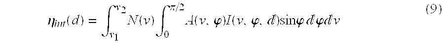
where A, I and the normalization factor N of Equation (5) now are functions of frequency. The limits of integration ν1, and ν2 are determined by G(ν) through A(ν,φ) (Equation (6)), which decays rapidly to zero beyond ±Γ from the center of the band ν0.
The description herein has focused on grating depths in the vicinity of d0. Similar results are obtained at odd multiples of d0(3d0, 5d0, etc.): the QE of a QWIP, with respect to detection of light that has a certain wavelength within the QWIP, is maximized when the depth of the grating is slightly more than an odd multiple of one-quarter of that wavelength.
While the invention has been described with respect to a limited number of embodiments, it will be appreciated that many variations, modifications and other applications of the invention may be made.
Claims (9)
1. A QWIP for detecting light of a certain frequency, the light having a certain wavelength when propagating within the QWIP, comprising:
(a) at least one planar quantum well; and
(b) a grating, parallel to said at least one planar quantum well, having a depth greater than an odd multiple of one-quarter of said wavelength and less than said odd multiple of about three-tenths of said wavelength.
2. The QWIP of claim 1, wherein said depth is between said odd multiple of about 0.2775 of said wavelength and said odd multiple of about three-tenths of said wavelength.
3. The QWIP of claim 5, wherein said depth is said odd multiple of about 0.2775 of said wavelength.
4. The QWIP of claim 3, wherein said odd multiple is a unit multiple.
5. The QWIP of claim 1, wherein said grating has a pitch selected to enhance scattering of the light by said grating within the QWIP in a direction parallel to the grating.
6. The QWIP of claim 1, wherein said grating has a pseudo-random lateral geometry.
7. A QWIP for detecting light of a certain frequency, comprising:
(a) at least one planar quantum well; and
(b) a grating, parallel to said at least one planar quantum well, and having at least one depth selected by estimating a quantum efficiency of the QWIP based on a scalar expression for an intensity of the light within the QWIP, said scalar expression being a function of said at least one depth.
8. The QWIP of claim 7, wherein said grating has a pitch selected to enhance scattering of the light by said grating within the QWIP in a direction parallel to the grating.
9. The QWIP of claim 7, wherein said grating has a pseudo-random lateral geometry.
Priority Applications (3)
| Application Number | Priority Date | Filing Date | Title |
|---|---|---|---|
| US09/123,487 US6172379B1 (en) | 1998-07-28 | 1998-07-28 | Method for optimizing QWIP grating depth |
| AU48696/99A AU4869699A (en) | 1998-07-28 | 1999-07-12 | Method for optimizing qwip grating depth |
| PCT/US1999/015641 WO2000007244A1 (en) | 1998-07-28 | 1999-07-12 | Method for optimizing qwip grating depth |
Applications Claiming Priority (1)
| Application Number | Priority Date | Filing Date | Title |
|---|---|---|---|
| US09/123,487 US6172379B1 (en) | 1998-07-28 | 1998-07-28 | Method for optimizing QWIP grating depth |
Publications (1)
| Publication Number | Publication Date |
|---|---|
| US6172379B1 true US6172379B1 (en) | 2001-01-09 |
Family
ID=22408948
Family Applications (1)
| Application Number | Title | Priority Date | Filing Date |
|---|---|---|---|
| US09/123,487 Expired - Fee Related US6172379B1 (en) | 1998-07-28 | 1998-07-28 | Method for optimizing QWIP grating depth |
Country Status (3)
| Country | Link |
|---|---|
| US (1) | US6172379B1 (en) |
| AU (1) | AU4869699A (en) |
| WO (1) | WO2000007244A1 (en) |
Cited By (1)
| Publication number | Priority date | Publication date | Assignee | Title |
|---|---|---|---|---|
| US20100037674A1 (en) * | 2008-03-21 | 2010-02-18 | The Regents Of The University Of California | Test Surfaces Useful for Calibration of Surface Profilometers |
Citations (8)
| Publication number | Priority date | Publication date | Assignee | Title |
|---|---|---|---|---|
| US5063419A (en) | 1988-11-15 | 1991-11-05 | The United States Of America As Represented By The Secretary Of The Navy | Heterostructure device useable as a far infrared photodetector |
| US5075749A (en) | 1989-12-29 | 1991-12-24 | At&T Bell Laboratories | Optical device including a grating |
| US5185647A (en) | 1988-12-12 | 1993-02-09 | The United States Of America As Represented By The Administrator Of The National Aeronautics And Space Administration | Long wavelength infrared detector |
| US5229614A (en) | 1991-04-08 | 1993-07-20 | Im Institutet Fur Mikroelektronik | Method of coupling radiation in an infrared detector, and an arrangement herefor |
| US5506419A (en) | 1994-11-10 | 1996-04-09 | At&T Corp. | Quantum well photodetector with pseudo-random reflection |
| US5784399A (en) * | 1996-12-19 | 1998-07-21 | Xerox Corporation | Polarization mode selection by distributed Bragg reflector in a quantum well laser |
| US5818066A (en) * | 1995-11-21 | 1998-10-06 | Thomson-Csf | Optoelectronic quantum well device having an optical resonant cavity and sustaining inter subband transitions |
| US6054718A (en) * | 1998-03-31 | 2000-04-25 | Lockheed Martin Corporation | Quantum well infrared photocathode having negative electron affinity surface |
Family Cites Families (2)
| Publication number | Priority date | Publication date | Assignee | Title |
|---|---|---|---|---|
| US5159420A (en) * | 1991-10-15 | 1992-10-27 | United Technologies Corporation | Dual medium heterojunction acoustic charge transport multiple quantum well spatial light modulator |
| US5650635A (en) * | 1995-07-14 | 1997-07-22 | Northwestern University | Multiple stacked Sb-based heterostructures |
-
1998
- 1998-07-28 US US09/123,487 patent/US6172379B1/en not_active Expired - Fee Related
-
1999
- 1999-07-12 AU AU48696/99A patent/AU4869699A/en not_active Abandoned
- 1999-07-12 WO PCT/US1999/015641 patent/WO2000007244A1/en active Application Filing
Patent Citations (8)
| Publication number | Priority date | Publication date | Assignee | Title |
|---|---|---|---|---|
| US5063419A (en) | 1988-11-15 | 1991-11-05 | The United States Of America As Represented By The Secretary Of The Navy | Heterostructure device useable as a far infrared photodetector |
| US5185647A (en) | 1988-12-12 | 1993-02-09 | The United States Of America As Represented By The Administrator Of The National Aeronautics And Space Administration | Long wavelength infrared detector |
| US5075749A (en) | 1989-12-29 | 1991-12-24 | At&T Bell Laboratories | Optical device including a grating |
| US5229614A (en) | 1991-04-08 | 1993-07-20 | Im Institutet Fur Mikroelektronik | Method of coupling radiation in an infrared detector, and an arrangement herefor |
| US5506419A (en) | 1994-11-10 | 1996-04-09 | At&T Corp. | Quantum well photodetector with pseudo-random reflection |
| US5818066A (en) * | 1995-11-21 | 1998-10-06 | Thomson-Csf | Optoelectronic quantum well device having an optical resonant cavity and sustaining inter subband transitions |
| US5784399A (en) * | 1996-12-19 | 1998-07-21 | Xerox Corporation | Polarization mode selection by distributed Bragg reflector in a quantum well laser |
| US6054718A (en) * | 1998-03-31 | 2000-04-25 | Lockheed Martin Corporation | Quantum well infrared photocathode having negative electron affinity surface |
Non-Patent Citations (16)
Cited By (2)
| Publication number | Priority date | Publication date | Assignee | Title |
|---|---|---|---|---|
| US20100037674A1 (en) * | 2008-03-21 | 2010-02-18 | The Regents Of The University Of California | Test Surfaces Useful for Calibration of Surface Profilometers |
| US8616044B2 (en) * | 2008-03-21 | 2013-12-31 | The Regents Of The University Of California | Test surfaces useful for calibration of surface profilometers |
Also Published As
| Publication number | Publication date |
|---|---|
| WO2000007244A1 (en) | 2000-02-10 |
| AU4869699A (en) | 2000-02-21 |
Similar Documents
| Publication | Publication Date | Title |
|---|---|---|
| US11049985B2 (en) | Photo detection device using resonance and related method | |
| JP5094385B2 (en) | High response high bandwidth metal-semiconductor-metal photoelectric device | |
| Andersson et al. | Near‐unity quantum efficiency of AlGaAs/GaAs quantum well infrared detectors using a waveguide with a doubly periodic grating coupler | |
| Andersson et al. | Quantum efficiency enhancement of AlGaAs/GaAs quantum well infrared detectors using a waveguide with a grating coupler | |
| US8704209B2 (en) | Photodetectors using resonance and method of making | |
| US6423980B1 (en) | Multi-directional radiation coupling in quantum-well infrared photodetectors | |
| US10957804B2 (en) | Photodetector using resonance and related method | |
| CN103811580B (en) | InGaAs infrared detector | |
| US9679091B2 (en) | Computer designed resonant photodetectors and method of making | |
| Levy-Yurista et al. | Very narrow spectral filters with multilayered grating-waveguide structures | |
| US5617436A (en) | Strain-compensated multiple quantum well laser structures | |
| Crouse | Numerical modeling and electromagnetic resonant modes in complex grating structures and optoelectronic device applications | |
| JP3645490B2 (en) | Coupling of wavelength insensitive radiation for multiple quantum well sensors based on intra-subband absorption | |
| US7211820B2 (en) | Quantum well sensor having spatially separated sensing columns | |
| US20110202323A1 (en) | Photodetectors using resonance and method of making | |
| US5506419A (en) | Quantum well photodetector with pseudo-random reflection | |
| Fu et al. | Optical coupling in quantum well infrared photodetector by diffraction grating | |
| US7745815B2 (en) | Polarization-sensitive quantum well infrared photodetector focal plane array | |
| US6172379B1 (en) | Method for optimizing QWIP grating depth | |
| Borenstain et al. | Optimized random/ordered grating for an n-type quantum well infrared photodetector | |
| Crouse et al. | A method for designing electromagnetic resonance enhanced silicon-on-insulator metal–semiconductor–metal photodetectors | |
| JP2000156513A (en) | Infrared detector and its manufacture | |
| JP5255042B2 (en) | Photodetector | |
| Fu et al. | Infrared radiation transmission through GaAs/AlGaAs quantum well infrared photodetector | |
| US20220200238A1 (en) | Laser comprising a distributed bragg mirror and production method |
Legal Events
| Date | Code | Title | Description |
|---|---|---|---|
| AS | Assignment |
Owner name: SAGI-NAHOR LTD., ISRAEL Free format text: ASSIGNMENT OF ASSIGNORS INTEREST;ASSIGNOR:BORENSTAIN, SHMUEL I.;REEL/FRAME:009353/0072 Effective date: 19980721 |
|
| REMI | Maintenance fee reminder mailed | ||
| LAPS | Lapse for failure to pay maintenance fees | ||
| LAPS | Lapse for failure to pay maintenance fees |
Free format text: PATENT EXPIRED FOR FAILURE TO PAY MAINTENANCE FEES (ORIGINAL EVENT CODE: EXP.); ENTITY STATUS OF PATENT OWNER: SMALL ENTITY |
|
| STCH | Information on status: patent discontinuation |
Free format text: PATENT EXPIRED DUE TO NONPAYMENT OF MAINTENANCE FEES UNDER 37 CFR 1.362 |
|
| FP | Lapsed due to failure to pay maintenance fee |
Effective date: 20050109 |