US6159869A - Method of making a circuit including a corral for containing a protective coating - Google Patents
Method of making a circuit including a corral for containing a protective coating Download PDFInfo
- Publication number
- US6159869A US6159869A US09/218,148 US21814898A US6159869A US 6159869 A US6159869 A US 6159869A US 21814898 A US21814898 A US 21814898A US 6159869 A US6159869 A US 6159869A
- Authority
- US
- United States
- Prior art keywords
- corral
- circuit
- forming
- active area
- coating
- Prior art date
- Legal status (The legal status is an assumption and is not a legal conclusion. Google has not performed a legal analysis and makes no representation as to the accuracy of the status listed.)
- Expired - Fee Related
Links
Images


Classifications
-
- H—ELECTRICITY
- H01—ELECTRIC ELEMENTS
- H01L—SEMICONDUCTOR DEVICES NOT COVERED BY CLASS H10
- H01L23/00—Details of semiconductor or other solid state devices
- H01L23/16—Fillings or auxiliary members in containers or encapsulations, e.g. centering rings
- H01L23/18—Fillings characterised by the material, its physical or chemical properties, or its arrangement within the complete device
- H01L23/24—Fillings characterised by the material, its physical or chemical properties, or its arrangement within the complete device solid or gel at the normal operating temperature of the device
-
- H—ELECTRICITY
- H01—ELECTRIC ELEMENTS
- H01L—SEMICONDUCTOR DEVICES NOT COVERED BY CLASS H10
- H01L23/00—Details of semiconductor or other solid state devices
- H01L23/28—Encapsulations, e.g. encapsulating layers, coatings, e.g. for protection
- H01L23/29—Encapsulations, e.g. encapsulating layers, coatings, e.g. for protection characterised by the material, e.g. carbon
- H01L23/293—Organic, e.g. plastic
-
- H—ELECTRICITY
- H01—ELECTRIC ELEMENTS
- H01L—SEMICONDUCTOR DEVICES NOT COVERED BY CLASS H10
- H01L23/00—Details of semiconductor or other solid state devices
- H01L23/28—Encapsulations, e.g. encapsulating layers, coatings, e.g. for protection
- H01L23/31—Encapsulations, e.g. encapsulating layers, coatings, e.g. for protection characterised by the arrangement or shape
- H01L23/3157—Partial encapsulation or coating
-
- H—ELECTRICITY
- H01—ELECTRIC ELEMENTS
- H01L—SEMICONDUCTOR DEVICES NOT COVERED BY CLASS H10
- H01L2224/00—Indexing scheme for arrangements for connecting or disconnecting semiconductor or solid-state bodies and methods related thereto as covered by H01L24/00
- H01L2224/01—Means for bonding being attached to, or being formed on, the surface to be connected, e.g. chip-to-package, die-attach, "first-level" interconnects; Manufacturing methods related thereto
- H01L2224/02—Bonding areas; Manufacturing methods related thereto
- H01L2224/04—Structure, shape, material or disposition of the bonding areas prior to the connecting process
- H01L2224/05—Structure, shape, material or disposition of the bonding areas prior to the connecting process of an individual bonding area
- H01L2224/0554—External layer
- H01L2224/0555—Shape
- H01L2224/05552—Shape in top view
- H01L2224/05554—Shape in top view being square
-
- H—ELECTRICITY
- H01—ELECTRIC ELEMENTS
- H01L—SEMICONDUCTOR DEVICES NOT COVERED BY CLASS H10
- H01L2224/00—Indexing scheme for arrangements for connecting or disconnecting semiconductor or solid-state bodies and methods related thereto as covered by H01L24/00
- H01L2224/01—Means for bonding being attached to, or being formed on, the surface to be connected, e.g. chip-to-package, die-attach, "first-level" interconnects; Manufacturing methods related thereto
- H01L2224/42—Wire connectors; Manufacturing methods related thereto
- H01L2224/47—Structure, shape, material or disposition of the wire connectors after the connecting process
- H01L2224/48—Structure, shape, material or disposition of the wire connectors after the connecting process of an individual wire connector
- H01L2224/481—Disposition
- H01L2224/48151—Connecting between a semiconductor or solid-state body and an item not being a semiconductor or solid-state body, e.g. chip-to-substrate, chip-to-passive
- H01L2224/48221—Connecting between a semiconductor or solid-state body and an item not being a semiconductor or solid-state body, e.g. chip-to-substrate, chip-to-passive the body and the item being stacked
- H01L2224/48245—Connecting between a semiconductor or solid-state body and an item not being a semiconductor or solid-state body, e.g. chip-to-substrate, chip-to-passive the body and the item being stacked the item being metallic
- H01L2224/48247—Connecting between a semiconductor or solid-state body and an item not being a semiconductor or solid-state body, e.g. chip-to-substrate, chip-to-passive the body and the item being stacked the item being metallic connecting the wire to a bond pad of the item
-
- H—ELECTRICITY
- H01—ELECTRIC ELEMENTS
- H01L—SEMICONDUCTOR DEVICES NOT COVERED BY CLASS H10
- H01L24/00—Arrangements for connecting or disconnecting semiconductor or solid-state bodies; Methods or apparatus related thereto
- H01L24/01—Means for bonding being attached to, or being formed on, the surface to be connected, e.g. chip-to-package, die-attach, "first-level" interconnects; Manufacturing methods related thereto
- H01L24/42—Wire connectors; Manufacturing methods related thereto
- H01L24/47—Structure, shape, material or disposition of the wire connectors after the connecting process
- H01L24/48—Structure, shape, material or disposition of the wire connectors after the connecting process of an individual wire connector
-
- H—ELECTRICITY
- H01—ELECTRIC ELEMENTS
- H01L—SEMICONDUCTOR DEVICES NOT COVERED BY CLASS H10
- H01L2924/00—Indexing scheme for arrangements or methods for connecting or disconnecting semiconductor or solid-state bodies as covered by H01L24/00
- H01L2924/0001—Technical content checked by a classifier
- H01L2924/00014—Technical content checked by a classifier the subject-matter covered by the group, the symbol of which is combined with the symbol of this group, being disclosed without further technical details
-
- H—ELECTRICITY
- H01—ELECTRIC ELEMENTS
- H01L—SEMICONDUCTOR DEVICES NOT COVERED BY CLASS H10
- H01L2924/00—Indexing scheme for arrangements or methods for connecting or disconnecting semiconductor or solid-state bodies as covered by H01L24/00
- H01L2924/10—Details of semiconductor or other solid state devices to be connected
- H01L2924/1015—Shape
- H01L2924/1016—Shape being a cuboid
- H01L2924/10161—Shape being a cuboid with a rectangular active surface
-
- H—ELECTRICITY
- H01—ELECTRIC ELEMENTS
- H01L—SEMICONDUCTOR DEVICES NOT COVERED BY CLASS H10
- H01L2924/00—Indexing scheme for arrangements or methods for connecting or disconnecting semiconductor or solid-state bodies as covered by H01L24/00
- H01L2924/10—Details of semiconductor or other solid state devices to be connected
- H01L2924/11—Device type
- H01L2924/14—Integrated circuits
Definitions
- the present invention relates to a circuit, more particularly, a circuit including a corral for containing a protective coating and a method of making same.
- Products such as circuits, may be reverse engineered to determine their design and operation.
- reverse engineering of a circuit may be performed by opening the package containing a circuit and viewing the components and interconnections that make up the circuit.
- the top layer of the circuit is viewed, then it is removed and the next later is viewed. That process may be repeated for each layer in the circuit.
- Layers may be viewed through a microscope or through the use of photography. Layers may be removed by a grinding process using a mild abrasive or through a chemical process.
- Products such as circuits, may be protected from reverse engineering by covering them with a protective coating to prevent reverse engineering.
- the protective coating is designed to conceal the circuit from visual inspection and to physically destroy the circuit if removed.
- the protective coating also prevents tampering with circuits and protects it from contaminants and outside forces that may damage the circuit, such as ultraviolet light and static electricity.
- Protective coatings come in many varieties, and the problems with the prior art generally apply to all such coatings.
- Primers are often used in conjunction with coatings Primers may have many functions including possessing inherent protective qualities and being an agent that will adhere to the surface of the circuit and to which the coating will adhere. It is important that coatings properly adhere so that they remain in place where they can serve their required function. Most tamper resistant materials are intended to destroy the circuit when removed. Therefore, adherence of tamper resistant materials is particularly important.
- the wires and package when employing the prior art method, must be attached to the circuit before the primer and tamper resistant coating are applied. That is because the primer and tamper resistant coating typically cover the bond pads, thereby preventing attachment to the bond pads at a later time.
- Another disadvantage to the prior art involves the risk to encryption codes, such as classified keys, which may be determined by examining an encrypted circuit prior to the application of the protective coating. Encryption typically requires access to the bond pads, so the prior art requires encryption to be performed prior to applying the protective coating. Therefore, such circuits are encoded prior to placement of the primer and tamper resistant coating, which may cover the bond pads, and remain unprotected until the protective coating is applied during packaging. As a result, greater security precautions are required to protect the circuit and encryption keys, thereby increasing the cost and potential for loss.
- the prior art also has an increased failure rate because classification keys can be erased or altered during the high temperature curing steps required after the application of the protective coating.
- the protective coating covering the bond pads prevents inspection of the bond pads after the circuit is completed. Because the bond pads cannot be inspected, it is more difficult to determine the cause of a failure.
- the protective coating also prevents defective wires arid contacts from being reworked. As a result, when a failure occurs in a circuit packaged in accordance with the prior art, the entire assembly must be discarded.
- prior art is not well suited for automated processing. For example, it is time consuming and cumbersome to load an automatic dispenser with individual circuits, as required by the prior art.
- prior art methods and devices require regular human interaction or additional machinery, such as a die picking apparatus. The benefit derived from an automated systems highly accurate placement of the material is also unrealized because the prior art allows the protective coating to flow onto the bond pads.
- the present invention is directed to a corral for a circuit.
- the corral is disposed on the circuit between the active area and one or more bond pads.
- the corral may be filled with a protective coating to prevent reverse engineering of the circuit.
- a primer may be used with the protective coating.
- the present invention is also directed to a method of forming a corral on a circuit.
- the method includes providing a circuit having an active area and one or more, bond pads and forming a corral on the circuit between the active area and bond pads.
- FIG. 1 is a top plan view of a circuit including a corral formed between an active area and bond pads;
- FIG. 2 is a cross-sectional view along line II--II of FIG. 1;
- FIG. 3 is a cross-sectional view of a circuit including a corral formed in two layers
- FIG. 4 is a cross-sectional view of a circuit including a coating bounded by the active area and the corral;
- FIG. 5 is a top plan view of a wafer including multiple circuits on which corrals are formed in accordance with the present invention
- FIG. 6 is a cross-sectional view of a circuit attached to a package
- FIG. 7 is a top plan view of a circuit of the present invention including a corral that partially covers the active area of the circuit;
- FIG. 8 is a top plan view of a circuit of the present invention including a corral that partially covers the bond pads of the circuit;
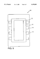
- FIG. 9 is a top plan view of a circuit of the present invention including a corral that partially covers both the active area and bond pads of the circuit.
- FIG. 1 is a top view of a circuit 10 including an active area 12, bond pads 14, and a corral 16 formed between the active area 2 and bond pads 14.
- the circuit 10 may be fabricated using any one of many different technologies, including silicon-on-insulator technology, silicon-on-sapphire technology, thin film transistor technology, and conventional silicon substrate technology.
- the term circuit is used in this application in a broad sense to include any circuit having a number of components connected together. An obvious example is an integrated circuit.
- a circuit also includes a circuit formed of discrete components on a circuit board, multi-chip modules and hybrid circuits.
- the corral 16 may be constructed from many materials and in many dimensions.
- the corral 16 may be formed on the circuit 10 between the active area 12 and the bond pads 14 so that the active area 12 may be covered by a coating 18 (illustrated in FIG. 4) and the bond pads 14 are not covered by the coating 18 (illustrated in FIG. 4).
- the corral 16 may, for example, touch neither the active area 12 nor the bond pads 14.
- the corral 16 may partially cover the active area 12 (illustrated in FIG. 7), or partially cover one or more bond pads 14, (illustrated in FIG. 8), or partially cover both the active area 12 and one or more bond pads 14 (illustrated in FIG. 9) although leaving enough of the bond pads 14 exposed for subsequent connections.
- the corral 16 may be formed of an electrically insulative, thermally capable, viscous adhesive, such as an epoxy resin. While an electrically insulative material is not necessary, it is beneficial, particularly if the corral 16 covers the active area 12 and/or one or more bond pads 14. For example, an electrically insulative corral 16 is desirable when the corral 16 touches the active area 12 and/or one or more bond pads 14 because it does not promote shorting of the active area 12 or the bond pads 14. A thermally curable material may also be used, such as when the circuit 10 includes materials that are cured after the corral 16 has been formed. Higher viscosity materials are often selected because their use allows a higher walled corral 16 to be formed in a single step. Adhesives are not required, although they may be used if a means of fastening the corral 16 to the circuit 10 is needed.
- the corral 16 may be built by selectively depositing or growing the walls of the corral 16. For example, an epoxy resin may be selectively deposited on the circuit 10 to form the corral 16. Alternatively, the corral 16 may be built by depositing or growing a material on all or part of the circuit 10 and then removing selected portions of that material to form the corral 16. For example, a photoresistive material may be placed over the entire circuit 10 and then selectively removed, such that a corral 16 of photoresistive material is formed around the active area 12. A corral 16 formed by a single application of a photoresistive material has been found to generally result in a lower corral 16 height than when formed by a single application of an epoxy resin.
- FIG. 2 is a cross-sectional view along line II--II of the circuit 10 illustrated in FIG. 1, illustrating the corral 16 formed on the surface of the circuit 10.
- the corral 16 illustrated in FIG. 2 is formed as a single piece or layer. However, the corral 16 may also be formed from multiple pieces or layers, as illustrated in FIG. 3. A corral 16 formed from multiple pieces or layers may be used in circumstances where the corral 16 must have a height that is greater than may be formed by a single layer of material.
- Such a corral 16 may be made by forming a first layer of the corral 16, curing the first layer, forming a second layer on top of the first layer, and then curing the second layer.
- a corral 16 may be pre-formed and placed on a circuit 10. In the pre-formed embodiment a complete corral 16 may be formed separate from the circuit 10 and then attached to the circuit 10.
- FIG. 4 is a cross sectional view of a circuit 10 after a protective coating 18 has be provided within the corral 16.
- the coating 18 covers the active area 12 and is within the boundaries formed by the corral 16.
- FIG. 4 illustrates the corral 16 partially filled with the protective coating 18, although the protective coating 18 may also completely fill the corral 16.
- the corral 16 may be removed after the active area 12 has been covered by the coating 18, leaving the protective coating 18 on the circuit 10.
- corrals 16 formed of photoresistive material may be removed by conventional techniques for removing photoresist. In practice, however, it has been found that it is unnecessary to remove the corral 16 because the corral 16 typically does not inhibit the functioning of the circuit 10. Furthermore, the additional handling and processing steps needed to remove the corral 16 add to the time and cost of fabricating the circuit 10, and may also increase the failure rate of the circuit 10.
- the corral 16 permits the coating 18 to be easily applied, either manually or automatically.
- the coating 18 will be evenly distributed within the corral 16 and will not interfere with the bond pads 14 or other components laying outside of the corral 16.
- the corral 16 also provides for greater protection from reverse engineering because the protective coating 18 covers the active area 12 at a uniform thickness and does not thin out at the edges.
- the corral 16 may be formed at any time after the circuit 10 is fabricated, thereby allowing the protective coating 18 to be applied at anytime thereafter.
- the circuit 10 can be protected earlier in the manufacturing process, thereby reducing the risk that the circuit 10 will be reverse engineered before it is packaged.
- Another advantage of applying the protective coating 18 early in the manufacturing process is that it allows the protective coating 18 to be applied before the encryption is coded onto the circuit 10, thereby eliminating a vulnerability present with the prior art.
- a circuit 10 that is encrypted after the protective coating 18 is applied may avoid a more restrictive classification by the government, thereby reducing handling and security costs.
- Yet another advantage of the present invention is that it allows a circuit 10 to be encrypted after the protective material 18 is cured, thereby eliminating the risk of exposing an encrypted circuit 10 to high curing temperatures and eliminating a source of failure in the prior art.
- corral 16 prevents the coating 18 from covering the bond pads 14, permitting visual inspection of the bond pads 14 and any connections to the bond pads 14. As a result, bond pads 14 and connections thereto may be reworked during subsequent processing and inspection steps.
- the protective material 18 may be any one or more of many materials, including tamper resistant materials, opaquing materials, and materials placed to protect the circuit 10 from outside forces including ultraviolet light, static electricity and impact.
- tamper resistant materials include epoxy resin mixtures, meshes, fibrous mixtures, ceramics, and alumina impregnated materials, such as zircon, topaz and garnet. Some of those materials also act as opaquing materials and offer protection from outside forces.
- the coating 18 may include more than one of those materials, and may also include a primer material.
- FIG. 5 illustrates a wafer 24 including a number of circuits 10, each having a corral 16. Coatings 18 may also be placed on the circuits 10 prior to dicing of the wafer 24.
- One reason for forming the corrals 16 and providing protective coatings 18 when the circuits 10 are in wafer form is that it affords a greater efficiency because a wafer 24 can generally be processed more quickly than diced circuits 10.
- the corral 16 may be formed and the protective coating 18 may be provided after the circuits 10 have been diced from a wafer 24.
- FIG. 6 is a cross-sectional view of the circuit 10 after wires 20 have been attached between the bond pads 14 and the package 22.
- the corral 16 prevents the coating 18 from covering the bond pads 14, thereby leaving the bond pads 14 exposed for later attachment by wires 20.
- Another advantage of the present invention is that when the protective coating 18 is provided early in the processing of the circuit, the wires 20 do not contact the protective coating 18 and are not exposed to high curing temperatures, thereby eliminating a source of failure in the prior art.
- the present invention also includes a method for forming a corral 16 on a circuit 10.
- the method includes providing a circuit including an active area 12 and one or more bond pads 14 and forming a corral 16 on the circuit 10 between the active area 12 and the bond pads 14.
- the corral 16 may be formed by many methods including, for example, automatic or manual formation or by attaching a pre-formed corral 16 to a circuit 10.
- a corral 16 of the present invention may be formed from one or more layers or pieces of corralling material. For example, if epoxy resin is used to form the corral 16, the first layer may be formed on the circuit 10 and the first layer may be cured at approximately 110° C. for a period of about 30 minutes.
- a second layer of epoxy resin may then be formed on top of the first layer and cured at approximately 170° C., for a period of about 60 to about 120 minutes. It will be obvious to those skilled in the art that other forming and curing steps may also be taken to achieve the resulting corral 16.
- Another method of forming a corral 16 of the present invention is by forming photoresistive material on a circuit 10 and then removing selected areas of photoresistive material to create a corral 16. Corrals 16 may also be removed. For example a corral 16 formed of photoresistive material, or epoxy resin on photoresistive material, may be removed by conventional process techniques.
- the present invention may include placing one or more coatings 18, such as primer and/or tamper resistant material, on the active area 12.
- coatings 18 such as primer and/or tamper resistant material
- Use of the corral 16 permits the placement of the coatings 18 early in the manufacture of a circuit 10. For example, placing coatings 18 on a circuit 10 may occur prior to encrypting the circuit 10.
- the present invention may also include a method for attaching a package 22 or wires 20 to a circuit 10 after a protective coating 18 is formed on the circuit 10.
- the package 22 may be attached to the circuit 10
- one end of a wire 20 may be attached to a bond pad 14 and the other end of the wire 20 may be attached to the package 22.
- Additional wires 20 may also be similarly attached. That is permitted because the corral 16 confines the coatings 18 to the active area 12 so that the bond pads 14 remain exposed.
- the prior art does not permit a package 22 or wires 20 to be attached after the coatings 18 are placed because the coatings 18 typically cover one or more of the bond pads 14 and once a bond pad 14 is covered it may no longer be used to attach the circuit 10 to the package 22.
- the present invention offers the additional benefit of permitting wires 20 to be inspected, reworked or removed and replaced with new wires 20. That is again possible because of the corral 16, which prevents coatings 18 from covering bond pads 14, thereby allowing access to the bond pads 14.
- FIG. 7 illustrates a corral 16 partially covering the active area 12 of a circuit 10.
- FIG. 8 illustrates a corral 16 partially covering the bond pads 14 of a circuit 10.
- FIG. 9 illustrates a corral 16 partially covering both the active area 12 and bond pads 14 of a circuit 10.
Abstract
Description
Claims (19)
Priority Applications (1)
| Application Number | Priority Date | Filing Date | Title |
|---|---|---|---|
| US09/218,148 US6159869A (en) | 1998-04-07 | 1998-12-21 | Method of making a circuit including a corral for containing a protective coating |
Applications Claiming Priority (2)
| Application Number | Priority Date | Filing Date | Title |
|---|---|---|---|
| US09/056,306 US5920112A (en) | 1998-04-07 | 1998-04-07 | Circuit including a corral for containing a protective coating, and method of making same |
| US09/218,148 US6159869A (en) | 1998-04-07 | 1998-12-21 | Method of making a circuit including a corral for containing a protective coating |
Related Parent Applications (1)
| Application Number | Title | Priority Date | Filing Date |
|---|---|---|---|
| US09/056,306 Division US5920112A (en) | 1998-04-07 | 1998-04-07 | Circuit including a corral for containing a protective coating, and method of making same |
Publications (1)
| Publication Number | Publication Date |
|---|---|
| US6159869A true US6159869A (en) | 2000-12-12 |
Family
ID=22003535
Family Applications (2)
| Application Number | Title | Priority Date | Filing Date |
|---|---|---|---|
| US09/056,306 Expired - Lifetime US5920112A (en) | 1998-04-07 | 1998-04-07 | Circuit including a corral for containing a protective coating, and method of making same |
| US09/218,148 Expired - Fee Related US6159869A (en) | 1998-04-07 | 1998-12-21 | Method of making a circuit including a corral for containing a protective coating |
Family Applications Before (1)
| Application Number | Title | Priority Date | Filing Date |
|---|---|---|---|
| US09/056,306 Expired - Lifetime US5920112A (en) | 1998-04-07 | 1998-04-07 | Circuit including a corral for containing a protective coating, and method of making same |
Country Status (1)
| Country | Link |
|---|---|
| US (2) | US5920112A (en) |
Cited By (3)
| Publication number | Priority date | Publication date | Assignee | Title |
|---|---|---|---|---|
| US20050284366A1 (en) * | 2003-01-10 | 2005-12-29 | Anderson Curtis W | Systems and methods for building tamper resistant coatings |
| US8886946B1 (en) * | 2002-09-04 | 2014-11-11 | Copilot Ventures Fund Iii Llc | Authentication method and system |
| US9811671B1 (en) | 2000-05-24 | 2017-11-07 | Copilot Ventures Fund Iii Llc | Authentication method and system |
Families Citing this family (7)
| Publication number | Priority date | Publication date | Assignee | Title |
|---|---|---|---|---|
| US5920112A (en) * | 1998-04-07 | 1999-07-06 | Micro Networks Corporation | Circuit including a corral for containing a protective coating, and method of making same |
| US6903451B1 (en) * | 1998-08-28 | 2005-06-07 | Samsung Electronics Co., Ltd. | Chip scale packages manufactured at wafer level |
| JP3583633B2 (en) * | 1998-12-21 | 2004-11-04 | シャープ株式会社 | Method for manufacturing semiconductor device |
| CN100370597C (en) * | 2004-07-09 | 2008-02-20 | 北京大学 | Measurability and safety design method for information safety IC |
| US8455990B2 (en) * | 2009-02-25 | 2013-06-04 | Conexant Systems, Inc. | Systems and methods of tamper proof packaging of a semiconductor device |
| US20100264522A1 (en) * | 2009-04-20 | 2010-10-21 | Chien-Pin Chen | Semiconductor device having at least one bump without overlapping specific pad or directly contacting specific pad |
| CN109496055B (en) * | 2017-09-13 | 2023-03-07 | 中兴通讯股份有限公司 | Assembly method and equipment of circuit structural member and circuit structural member |
Citations (13)
| Publication number | Priority date | Publication date | Assignee | Title |
|---|---|---|---|---|
| US4663190A (en) * | 1984-03-08 | 1987-05-05 | Hitachi Chemical Company, Ltd. | Process for producing semiconductor element |
| US4771330A (en) * | 1987-05-13 | 1988-09-13 | Lsi Logic Corporation | Wire bonds and electrical contacts of an integrated circuit device |
| US4821151A (en) * | 1985-12-20 | 1989-04-11 | Olin Corporation | Hermetically sealed package |
| US5030796A (en) * | 1989-08-11 | 1991-07-09 | Rockwell International Corporation | Reverse-engineering resistant encapsulant for microelectric device |
| US5258334A (en) * | 1993-01-15 | 1993-11-02 | The U.S. Government As Represented By The Director, National Security Agency | Process of preventing visual access to a semiconductor device by applying an opaque ceramic coating to integrated circuit devices |
| US5258575A (en) * | 1990-05-07 | 1993-11-02 | Kyocera America, Inc. | Ceramic glass integrated circuit package with integral ground and power planes |
| US5311060A (en) * | 1989-12-19 | 1994-05-10 | Lsi Logic Corporation | Heat sink for semiconductor device assembly |
| US5468990A (en) * | 1993-07-22 | 1995-11-21 | National Semiconductor Corp. | Structures for preventing reverse engineering of integrated circuits |
| US5729437A (en) * | 1994-06-22 | 1998-03-17 | Seiko Epson Corporation | Electronic part including a thin body of molding resin |
| US5861662A (en) * | 1997-02-24 | 1999-01-19 | General Instrument Corporation | Anti-tamper bond wire shield for an integrated circuit |
| US5877093A (en) * | 1995-10-27 | 1999-03-02 | Honeywell Inc. | Process for coating an integrated circuit device with a molten spray |
| US5920112A (en) * | 1998-04-07 | 1999-07-06 | Micro Networks Corporation | Circuit including a corral for containing a protective coating, and method of making same |
| US6002181A (en) * | 1994-11-08 | 1999-12-14 | Oki Electric Industry Co., Ltd. | Structure of resin molded type semiconductor device with embedded thermal dissipator |
Family Cites Families (1)
| Publication number | Priority date | Publication date | Assignee | Title |
|---|---|---|---|---|
| US5583375A (en) * | 1990-06-11 | 1996-12-10 | Hitachi, Ltd. | Semiconductor device with lead structure within the planar area of the device |
-
1998
- 1998-04-07 US US09/056,306 patent/US5920112A/en not_active Expired - Lifetime
- 1998-12-21 US US09/218,148 patent/US6159869A/en not_active Expired - Fee Related
Patent Citations (14)
| Publication number | Priority date | Publication date | Assignee | Title |
|---|---|---|---|---|
| US4663190A (en) * | 1984-03-08 | 1987-05-05 | Hitachi Chemical Company, Ltd. | Process for producing semiconductor element |
| US4821151A (en) * | 1985-12-20 | 1989-04-11 | Olin Corporation | Hermetically sealed package |
| US4771330A (en) * | 1987-05-13 | 1988-09-13 | Lsi Logic Corporation | Wire bonds and electrical contacts of an integrated circuit device |
| US5030796A (en) * | 1989-08-11 | 1991-07-09 | Rockwell International Corporation | Reverse-engineering resistant encapsulant for microelectric device |
| US5311060A (en) * | 1989-12-19 | 1994-05-10 | Lsi Logic Corporation | Heat sink for semiconductor device assembly |
| US5258575A (en) * | 1990-05-07 | 1993-11-02 | Kyocera America, Inc. | Ceramic glass integrated circuit package with integral ground and power planes |
| US5258334A (en) * | 1993-01-15 | 1993-11-02 | The U.S. Government As Represented By The Director, National Security Agency | Process of preventing visual access to a semiconductor device by applying an opaque ceramic coating to integrated circuit devices |
| US5468990A (en) * | 1993-07-22 | 1995-11-21 | National Semiconductor Corp. | Structures for preventing reverse engineering of integrated circuits |
| US5821582A (en) * | 1993-07-22 | 1998-10-13 | National Semiconductor Corp. | Structures for preventing reverse engineering of integrated circuits |
| US5729437A (en) * | 1994-06-22 | 1998-03-17 | Seiko Epson Corporation | Electronic part including a thin body of molding resin |
| US6002181A (en) * | 1994-11-08 | 1999-12-14 | Oki Electric Industry Co., Ltd. | Structure of resin molded type semiconductor device with embedded thermal dissipator |
| US5877093A (en) * | 1995-10-27 | 1999-03-02 | Honeywell Inc. | Process for coating an integrated circuit device with a molten spray |
| US5861662A (en) * | 1997-02-24 | 1999-01-19 | General Instrument Corporation | Anti-tamper bond wire shield for an integrated circuit |
| US5920112A (en) * | 1998-04-07 | 1999-07-06 | Micro Networks Corporation | Circuit including a corral for containing a protective coating, and method of making same |
Cited By (5)
| Publication number | Priority date | Publication date | Assignee | Title |
|---|---|---|---|---|
| US9811671B1 (en) | 2000-05-24 | 2017-11-07 | Copilot Ventures Fund Iii Llc | Authentication method and system |
| US8886946B1 (en) * | 2002-09-04 | 2014-11-11 | Copilot Ventures Fund Iii Llc | Authentication method and system |
| US9818249B1 (en) | 2002-09-04 | 2017-11-14 | Copilot Ventures Fund Iii Llc | Authentication method and system |
| US20050284366A1 (en) * | 2003-01-10 | 2005-12-29 | Anderson Curtis W | Systems and methods for building tamper resistant coatings |
| US8210120B2 (en) | 2003-01-10 | 2012-07-03 | Microsemi Corporation | Systems and methods for building tamper resistant coatings |
Also Published As
| Publication number | Publication date |
|---|---|
| US5920112A (en) | 1999-07-06 |
Similar Documents
| Publication | Publication Date | Title |
|---|---|---|
| US6159869A (en) | Method of making a circuit including a corral for containing a protective coating | |
| US6316290B1 (en) | Method of fabricating a semiconductor device utilizing a residual organic compound to facilitate gate break on a carrier substrate | |
| USRE38789E1 (en) | Semiconductor wafer having a bottom surface protective coating | |
| US8252408B2 (en) | Electronic device and method of manufacturing the electronic device | |
| US5980683A (en) | Production of a support element module for embedding into smart cards or other data carrier cards | |
| CA1232372A (en) | Method for encapsulating semiconductor components mounted on a carrier tape | |
| CN108257882A (en) | The method of stress release in device encapsulation structure and encapsulation process | |
| KR100557286B1 (en) | A semiconductor chip and process for producing a semiconductor chip | |
| US6794225B2 (en) | Surface treatment for microelectronic device substrate | |
| EP0124624A4 (en) | Semiconductor device. | |
| US8399296B2 (en) | Airgap micro-spring interconnect with bonded underfill seal | |
| US6404069B2 (en) | Use of oxide surface to facilitate gate break on a carrier substrate for a semiconductor device | |
| US7041536B2 (en) | Semiconductor integrated circuit card manufacturing method, and semiconductor integrated circuit card | |
| US6686015B2 (en) | Transferable resilient element for packaging of a semiconductor chip and method therefor | |
| US6484394B1 (en) | Encapsulation method for ball grid array semiconductor package | |
| US6090237A (en) | Apparatus for restraining adhesive overflow in a multilayer substrate assembly during lamination | |
| JPH0745641A (en) | Semiconductor device mounting method | |
| US6300162B1 (en) | Method of applying a protective layer to a microelectronic component | |
| US20020167078A1 (en) | Electronic component with a semiconductor chip and method of producing an electronic component | |
| US5264726A (en) | Chip-carrier | |
| US6528354B1 (en) | Method of manufacturing a semiconductor device | |
| US7235425B2 (en) | Semiconductor device and fabrication method for the same | |
| CN100515150C (en) | Method for bonding a glass cap and mask for curing sealant | |
| EP1514234B1 (en) | Tape manufacturing | |
| JPS5891663A (en) | Semiconductor device and manufacture thereof |
Legal Events
| Date | Code | Title | Description |
|---|---|---|---|
| AS | Assignment |
Owner name: MNC WORCESTER CORPORATION, MASSACHUSETTS Free format text: CHANGE OF NAME;ASSIGNOR:MICRO NETWORKS CORPORATION;REEL/FRAME:012083/0865 Effective date: 19990713 |
|
| AS | Assignment |
Owner name: CITIZENS BANK OF MASSACHUSETTS, MASSACHUSETTS Free format text: ASSIGNMENT OF ASSIGNORS INTEREST;ASSIGNOR:MNC WORCESTER CORPORATION;REEL/FRAME:012124/0556 Effective date: 20010706 |
|
| CC | Certificate of correction | ||
| FEPP | Fee payment procedure |
Free format text: PAYOR NUMBER ASSIGNED (ORIGINAL EVENT CODE: ASPN); ENTITY STATUS OF PATENT OWNER: LARGE ENTITY Free format text: PAT HOLDER NO LONGER CLAIMS SMALL ENTITY STATUS, ENTITY STATUS SET TO UNDISCOUNTED (ORIGINAL EVENT CODE: STOL); ENTITY STATUS OF PATENT OWNER: LARGE ENTITY |
|
| REFU | Refund |
Free format text: REFUND - SURCHARGE, PETITION TO ACCEPT PYMT AFTER EXP, UNINTENTIONAL (ORIGINAL EVENT CODE: R2551); ENTITY STATUS OF PATENT OWNER: LARGE ENTITY |
|
| AS | Assignment |
Owner name: ICS TECHNOLOGIES, INC., DELAWARE Free format text: ASSIGNMENT OF ASSIGNORS INTEREST;ASSIGNOR:MNC WORCESTER CORPORATION.;REEL/FRAME:015242/0792 Effective date: 20040206 |
|
| AS | Assignment |
Owner name: MNC WORCESTER CORPORATION, MASSACHUSETTS Free format text: RELEASE OF SECURITY INTEREST;ASSIGNOR:CITIZENS BANK OF MASSACHUSETTS;REEL/FRAME:015320/0837 Effective date: 20040406 |
|
| FPAY | Fee payment |
Year of fee payment: 4 |
|
| AS | Assignment |
Owner name: INTEGRATED DEVICE TECHNOLOGY, INC., CALIFORNIA Free format text: ASSIGNMENT OF ASSIGNORS INTEREST;ASSIGNOR:ICS TECHNOLOGIES, INC.;REEL/FRAME:018279/0284 Effective date: 20060920 |
|
| REMI | Maintenance fee reminder mailed | ||
| FPAY | Fee payment |
Year of fee payment: 8 |
|
| SULP | Surcharge for late payment |
Year of fee payment: 7 |
|
| AS | Assignment |
Owner name: SPECTRUM MICROWAVE, INC., PENNSYLVANIA Free format text: ASSIGNMENT OF ASSIGNORS INTEREST;ASSIGNOR:INTEGRATED DEVICE TECHNOLOGY, INC.;REEL/FRAME:023699/0811 Effective date: 20091130 |
|
| REMI | Maintenance fee reminder mailed | ||
| LAPS | Lapse for failure to pay maintenance fees | ||
| STCH | Information on status: patent discontinuation |
Free format text: PATENT EXPIRED DUE TO NONPAYMENT OF MAINTENANCE FEES UNDER 37 CFR 1.362 |
|
| FP | Lapsed due to failure to pay maintenance fee |
Effective date: 20121212 |
|
| AS | Assignment |
Owner name: SPECTRUM MICROWAVE, INC., PENNSYLVANIA Free format text: RELEASE BY SECURED PARTY;ASSIGNOR:MORGAN STANLEY SENIOR FUNDING, INC.;REEL/FRAME:029767/0683 Effective date: 20130206 |
|
| AS | Assignment |
Owner name: GUGGENHEIM CORPORATE FUNDING, LLC, NEW YORK Free format text: PATENT SECURITY AGREEMENT;ASSIGNORS:SPECTRUM MICROWAVE, INC.;API CRYPTEK INC.;API DEFENSE, INC.;AND OTHERS;REEL/FRAME:029777/0130 Effective date: 20130206 |
|
| AS | Assignment |
Owner name: WELLS FARGO BANK, NATIONAL ASSOCIATION (AS AGENT), Free format text: SECURITY AGREEMENT;ASSIGNORS:API DEFENSE. INC.;NATIONAL HYBRID. INC.,;API CRYPTEK INC.;AND OTHERS;REEL/FRAME:029800/0494 Effective date: 20130206 |
|
| AS | Assignment |
Owner name: SPECTRUM MICROWAVE, INC., PENNSYLVANIA Free format text: RELEASE BY SECURED PARTY;ASSIGNOR:WELLS FARGO BANK, NATIONAL ASSOCIATION, AS AGENT;REEL/FRAME:032501/0458 Effective date: 20140321 Owner name: API CRYPTEK INC., PENNSYLVANIA Free format text: RELEASE BY SECURED PARTY;ASSIGNOR:WELLS FARGO BANK, NATIONAL ASSOCIATION, AS AGENT;REEL/FRAME:032501/0458 Effective date: 20140321 Owner name: SPECTRUM CONTROL, INC., PENNSYLVANIA Free format text: RELEASE BY SECURED PARTY;ASSIGNOR:WELLS FARGO BANK, NATIONAL ASSOCIATION, AS AGENT;REEL/FRAME:032501/0458 Effective date: 20140321 Owner name: API DEFENSE, INC., PENNSYLVANIA Free format text: RELEASE BY SECURED PARTY;ASSIGNOR:WELLS FARGO BANK, NATIONAL ASSOCIATION, AS AGENT;REEL/FRAME:032501/0458 Effective date: 20140321 Owner name: API NANOFABRICATION AND RESEARCH CORPORATION, FLOR Free format text: RELEASE BY SECURED PARTY;ASSIGNOR:WELLS FARGO BANK, NATIONAL ASSOCIATION, AS AGENT;REEL/FRAME:032501/0458 Effective date: 20140321 Owner name: NATIONAL HYBRID, INC., NEW YORK Free format text: RELEASE BY SECURED PARTY;ASSIGNOR:WELLS FARGO BANK, NATIONAL ASSOCIATION, AS AGENT;REEL/FRAME:032501/0458 Effective date: 20140321 |
|
| AS | Assignment |
Owner name: NATIONAL HYBRID, INC., NEW YORK Free format text: RELEASE BY SECURED PARTY;ASSIGNOR:GUGGENHEIM CORPORATE FUNDING, LLC, AS AGENT;REEL/FRAME:038502/0459 Effective date: 20160422 Owner name: API DEFENSE, INC., PENNSYLVANIA Free format text: RELEASE BY SECURED PARTY;ASSIGNOR:GUGGENHEIM CORPORATE FUNDING, LLC, AS AGENT;REEL/FRAME:038502/0459 Effective date: 20160422 Owner name: API CRYPTEK INC., PENNSYLVANIA Free format text: RELEASE BY SECURED PARTY;ASSIGNOR:GUGGENHEIM CORPORATE FUNDING, LLC, AS AGENT;REEL/FRAME:038502/0459 Effective date: 20160422 Owner name: SPECTRUM CONTROL, INC., PENNSYLVANIA Free format text: RELEASE BY SECURED PARTY;ASSIGNOR:GUGGENHEIM CORPORATE FUNDING, LLC, AS AGENT;REEL/FRAME:038502/0459 Effective date: 20160422 Owner name: API NANOFABRICATION AND RESEARCH CORPORATION, FLOR Free format text: RELEASE BY SECURED PARTY;ASSIGNOR:GUGGENHEIM CORPORATE FUNDING, LLC, AS AGENT;REEL/FRAME:038502/0459 Effective date: 20160422 Owner name: SPECTRUM MICROWAVE, INC., PENNSYLVANIA Free format text: RELEASE BY SECURED PARTY;ASSIGNOR:GUGGENHEIM CORPORATE FUNDING, LLC, AS AGENT;REEL/FRAME:038502/0459 Effective date: 20160422 |
|
| AS | Assignment |
Owner name: ANTARES CAPITAL LP, AS AGENT, ILLINOIS Free format text: SECURITY INTEREST;ASSIGNORS:API TECHNOLOGIES CORP.;SPECTRUM CONTROL, INC.;SPECTRUM MICROWAVE, INC.;REEL/FRAME:045595/0601 Effective date: 20180420 |
|
| AS | Assignment |
Owner name: SPECTRUM MICROWAVE, INC., MASSACHUSETTS Free format text: RELEASE BY SECURED PARTY;ASSIGNOR:ANTARES CAPITAL LP;REEL/FRAME:049132/0139 Effective date: 20190509 Owner name: SPECTRUM CONTROL, INC., PENNSYLVANIA Free format text: RELEASE BY SECURED PARTY;ASSIGNOR:ANTARES CAPITAL LP;REEL/FRAME:049132/0139 Effective date: 20190509 Owner name: API TECHNOLOGIES, CORP, FLORIDA Free format text: RELEASE BY SECURED PARTY;ASSIGNOR:ANTARES CAPITAL LP;REEL/FRAME:049132/0139 Effective date: 20190509 |