US6153935A - Dual etch stop/diffusion barrier for damascene interconnects - Google Patents
Dual etch stop/diffusion barrier for damascene interconnects Download PDFInfo
- Publication number
- US6153935A US6153935A US09/409,244 US40924499A US6153935A US 6153935 A US6153935 A US 6153935A US 40924499 A US40924499 A US 40924499A US 6153935 A US6153935 A US 6153935A
- Authority
- US
- United States
- Prior art keywords
- conductive
- conductive material
- diffusion barrier
- stop
- layer
- Prior art date
- Legal status (The legal status is an assumption and is not a legal conclusion. Google has not performed a legal analysis and makes no representation as to the accuracy of the status listed.)
- Expired - Lifetime
Links
- 230000004888 barrier function Effects 0.000 title claims abstract description 69
- 238000009792 diffusion process Methods 0.000 title claims abstract description 68
- 230000009977 dual effect Effects 0.000 title abstract description 3
- 239000004020 conductor Substances 0.000 claims abstract description 92
- 229910052751 metal Inorganic materials 0.000 claims abstract description 64
- 239000002184 metal Substances 0.000 claims abstract description 64
- 239000010949 copper Substances 0.000 claims abstract description 45
- RYGMFSIKBFXOCR-UHFFFAOYSA-N Copper Chemical compound [Cu] RYGMFSIKBFXOCR-UHFFFAOYSA-N 0.000 claims abstract description 44
- 229910052802 copper Inorganic materials 0.000 claims abstract description 43
- 239000000126 substance Substances 0.000 claims abstract description 16
- 239000000758 substrate Substances 0.000 claims description 31
- KDLHZDBZIXYQEI-UHFFFAOYSA-N Palladium Chemical compound [Pd] KDLHZDBZIXYQEI-UHFFFAOYSA-N 0.000 claims description 15
- 229910052782 aluminium Inorganic materials 0.000 claims description 9
- XAGFODPZIPBFFR-UHFFFAOYSA-N aluminium Chemical compound [Al] XAGFODPZIPBFFR-UHFFFAOYSA-N 0.000 claims description 9
- 229910052763 palladium Inorganic materials 0.000 claims description 8
- 229910052698 phosphorus Inorganic materials 0.000 claims description 8
- 229910052721 tungsten Inorganic materials 0.000 claims description 8
- 239000010937 tungsten Substances 0.000 claims description 8
- 229910052738 indium Inorganic materials 0.000 claims description 7
- APFVFJFRJDLVQX-UHFFFAOYSA-N indium atom Chemical compound [In] APFVFJFRJDLVQX-UHFFFAOYSA-N 0.000 claims description 7
- 239000000203 mixture Substances 0.000 claims description 7
- WFKWXMTUELFFGS-UHFFFAOYSA-N tungsten Chemical compound [W] WFKWXMTUELFFGS-UHFFFAOYSA-N 0.000 claims description 7
- 229910052581 Si3N4 Inorganic materials 0.000 claims description 6
- ATJFFYVFTNAWJD-UHFFFAOYSA-N Tin Chemical compound [Sn] ATJFFYVFTNAWJD-UHFFFAOYSA-N 0.000 claims description 6
- HQVNEWCFYHHQES-UHFFFAOYSA-N silicon nitride Chemical group N12[Si]34N5[Si]62N3[Si]51N64 HQVNEWCFYHHQES-UHFFFAOYSA-N 0.000 claims description 6
- 229910052718 tin Inorganic materials 0.000 claims description 6
- BQCADISMDOOEFD-UHFFFAOYSA-N Silver Chemical compound [Ag] BQCADISMDOOEFD-UHFFFAOYSA-N 0.000 claims description 5
- 229910045601 alloy Inorganic materials 0.000 claims description 5
- 239000000956 alloy Substances 0.000 claims description 5
- PCHJSUWPFVWCPO-UHFFFAOYSA-N gold Chemical compound [Au] PCHJSUWPFVWCPO-UHFFFAOYSA-N 0.000 claims description 5
- 229910052737 gold Inorganic materials 0.000 claims description 5
- 239000010931 gold Substances 0.000 claims description 5
- 229910052709 silver Inorganic materials 0.000 claims description 5
- 239000004332 silver Substances 0.000 claims description 5
- 238000000034 method Methods 0.000 abstract description 50
- 230000008021 deposition Effects 0.000 abstract description 17
- 238000000151 deposition Methods 0.000 description 27
- 230000008569 process Effects 0.000 description 25
- 239000000463 material Substances 0.000 description 22
- VYPSYNLAJGMNEJ-UHFFFAOYSA-N Silicium dioxide Chemical compound O=[Si]=O VYPSYNLAJGMNEJ-UHFFFAOYSA-N 0.000 description 18
- 150000002500 ions Chemical class 0.000 description 16
- 230000015572 biosynthetic process Effects 0.000 description 13
- 238000005498 polishing Methods 0.000 description 11
- 238000005229 chemical vapour deposition Methods 0.000 description 9
- 239000000377 silicon dioxide Substances 0.000 description 9
- 239000002002 slurry Substances 0.000 description 7
- XUIMIQQOPSSXEZ-UHFFFAOYSA-N Silicon Chemical compound [Si] XUIMIQQOPSSXEZ-UHFFFAOYSA-N 0.000 description 5
- 238000005240 physical vapour deposition Methods 0.000 description 5
- 239000004065 semiconductor Substances 0.000 description 5
- 229910052710 silicon Inorganic materials 0.000 description 5
- 239000010703 silicon Substances 0.000 description 5
- 235000012239 silicon dioxide Nutrition 0.000 description 5
- MHAJPDPJQMAIIY-UHFFFAOYSA-N Hydrogen peroxide Chemical compound OO MHAJPDPJQMAIIY-UHFFFAOYSA-N 0.000 description 4
- 239000008139 complexing agent Substances 0.000 description 4
- 238000010586 diagram Methods 0.000 description 4
- 229920002120 photoresistant polymer Polymers 0.000 description 4
- 239000000243 solution Substances 0.000 description 4
- KWYUFKZDYYNOTN-UHFFFAOYSA-M Potassium hydroxide Chemical compound [OH-].[K+] KWYUFKZDYYNOTN-UHFFFAOYSA-M 0.000 description 3
- QAOWNCQODCNURD-UHFFFAOYSA-N Sulfuric acid Chemical compound OS(O)(=O)=O QAOWNCQODCNURD-UHFFFAOYSA-N 0.000 description 3
- JUZTWRXHHZRLED-UHFFFAOYSA-N [Si].[Cu].[Cu].[Cu].[Cu].[Cu] Chemical compound [Si].[Cu].[Cu].[Cu].[Cu].[Cu] JUZTWRXHHZRLED-UHFFFAOYSA-N 0.000 description 3
- PNEYBMLMFCGWSK-UHFFFAOYSA-N aluminium oxide Inorganic materials [O-2].[O-2].[O-2].[Al+3].[Al+3] PNEYBMLMFCGWSK-UHFFFAOYSA-N 0.000 description 3
- 238000005234 chemical deposition Methods 0.000 description 3
- 229910021360 copper silicide Inorganic materials 0.000 description 3
- 238000005260 corrosion Methods 0.000 description 3
- 230000007797 corrosion Effects 0.000 description 3
- 238000005530 etching Methods 0.000 description 3
- 238000001704 evaporation Methods 0.000 description 3
- 230000008020 evaporation Effects 0.000 description 3
- 230000001590 oxidative effect Effects 0.000 description 3
- 238000004544 sputter deposition Methods 0.000 description 3
- QGZKDVFQNNGYKY-UHFFFAOYSA-O Ammonium Chemical compound [NH4+] QGZKDVFQNNGYKY-UHFFFAOYSA-O 0.000 description 2
- XKRFYHLGVUSROY-UHFFFAOYSA-N Argon Chemical compound [Ar] XKRFYHLGVUSROY-UHFFFAOYSA-N 0.000 description 2
- IJGRMHOSHXDMSA-UHFFFAOYSA-N Atomic nitrogen Chemical compound N#N IJGRMHOSHXDMSA-UHFFFAOYSA-N 0.000 description 2
- ROFVEXUMMXZLPA-UHFFFAOYSA-N Bipyridyl Chemical group N1=CC=CC=C1C1=CC=CC=N1 ROFVEXUMMXZLPA-UHFFFAOYSA-N 0.000 description 2
- KFSLWBXXFJQRDL-UHFFFAOYSA-N Peracetic acid Chemical compound CC(=O)OO KFSLWBXXFJQRDL-UHFFFAOYSA-N 0.000 description 2
- NBIIXXVUZAFLBC-UHFFFAOYSA-N Phosphoric acid Chemical compound OP(O)(O)=O NBIIXXVUZAFLBC-UHFFFAOYSA-N 0.000 description 2
- OAICVXFJPJFONN-UHFFFAOYSA-N Phosphorus Chemical compound [P] OAICVXFJPJFONN-UHFFFAOYSA-N 0.000 description 2
- 229910007277 Si3 N4 Inorganic materials 0.000 description 2
- GWEVSGVZZGPLCZ-UHFFFAOYSA-N Titan oxide Chemical compound O=[Ti]=O GWEVSGVZZGPLCZ-UHFFFAOYSA-N 0.000 description 2
- 230000004913 activation Effects 0.000 description 2
- ROOXNKNUYICQNP-UHFFFAOYSA-N ammonium persulfate Chemical compound [NH4+].[NH4+].[O-]S(=O)(=O)OOS([O-])(=O)=O ROOXNKNUYICQNP-UHFFFAOYSA-N 0.000 description 2
- BFNBIHQBYMNNAN-UHFFFAOYSA-N ammonium sulfate Chemical compound N.N.OS(O)(=O)=O BFNBIHQBYMNNAN-UHFFFAOYSA-N 0.000 description 2
- 229910052921 ammonium sulfate Inorganic materials 0.000 description 2
- 235000011130 ammonium sulphate Nutrition 0.000 description 2
- 239000012298 atmosphere Substances 0.000 description 2
- CETPSERCERDGAM-UHFFFAOYSA-N ceric oxide Chemical compound O=[Ce]=O CETPSERCERDGAM-UHFFFAOYSA-N 0.000 description 2
- 229910000422 cerium(IV) oxide Inorganic materials 0.000 description 2
- 239000003989 dielectric material Substances 0.000 description 2
- 238000007772 electroless plating Methods 0.000 description 2
- ZOOODBUHSVUZEM-UHFFFAOYSA-N ethoxymethanedithioic acid Chemical compound CCOC(S)=S ZOOODBUHSVUZEM-UHFFFAOYSA-N 0.000 description 2
- 239000007789 gas Substances 0.000 description 2
- 239000011521 glass Substances 0.000 description 2
- 230000006872 improvement Effects 0.000 description 2
- 239000003112 inhibitor Substances 0.000 description 2
- 239000012212 insulator Substances 0.000 description 2
- 238000004519 manufacturing process Methods 0.000 description 2
- 150000002739 metals Chemical class 0.000 description 2
- 230000007935 neutral effect Effects 0.000 description 2
- 239000007800 oxidant agent Substances 0.000 description 2
- 230000003071 parasitic effect Effects 0.000 description 2
- 239000011574 phosphorus Substances 0.000 description 2
- 238000000206 photolithography Methods 0.000 description 2
- 238000001020 plasma etching Methods 0.000 description 2
- 238000000623 plasma-assisted chemical vapour deposition Methods 0.000 description 2
- -1 poly-arylene ether Chemical compound 0.000 description 2
- 150000003839 salts Chemical class 0.000 description 2
- 239000005368 silicate glass Substances 0.000 description 2
- HBMJWWWQQXIZIP-UHFFFAOYSA-N silicon carbide Chemical compound [Si+]#[C-] HBMJWWWQQXIZIP-UHFFFAOYSA-N 0.000 description 2
- 239000002210 silicon-based material Substances 0.000 description 2
- 239000004094 surface-active agent Substances 0.000 description 2
- MZLGASXMSKOWSE-UHFFFAOYSA-N tantalum nitride Chemical compound [Ta]#N MZLGASXMSKOWSE-UHFFFAOYSA-N 0.000 description 2
- 150000003573 thiols Chemical class 0.000 description 2
- UMGDCJDMYOKAJW-UHFFFAOYSA-N thiourea Chemical compound NC(N)=S UMGDCJDMYOKAJW-UHFFFAOYSA-N 0.000 description 2
- 150000003585 thioureas Chemical class 0.000 description 2
- 239000012991 xanthate Substances 0.000 description 2
- LCPVQAHEFVXVKT-UHFFFAOYSA-N 2-(2,4-difluorophenoxy)pyridin-3-amine Chemical compound NC1=CC=CN=C1OC1=CC=C(F)C=C1F LCPVQAHEFVXVKT-UHFFFAOYSA-N 0.000 description 1
- VHUUQVKOLVNVRT-UHFFFAOYSA-N Ammonium hydroxide Chemical compound [NH4+].[OH-] VHUUQVKOLVNVRT-UHFFFAOYSA-N 0.000 description 1
- OKTJSMMVPCPJKN-UHFFFAOYSA-N Carbon Chemical compound [C] OKTJSMMVPCPJKN-UHFFFAOYSA-N 0.000 description 1
- UGFAIRIUMAVXCW-UHFFFAOYSA-N Carbon monoxide Chemical compound [O+]#[C-] UGFAIRIUMAVXCW-UHFFFAOYSA-N 0.000 description 1
- KRKNYBCHXYNGOX-UHFFFAOYSA-K Citrate Chemical compound [O-]C(=O)CC(O)(CC([O-])=O)C([O-])=O KRKNYBCHXYNGOX-UHFFFAOYSA-K 0.000 description 1
- KCXVZYZYPLLWCC-UHFFFAOYSA-N EDTA Chemical compound OC(=O)CN(CC(O)=O)CCN(CC(O)=O)CC(O)=O KCXVZYZYPLLWCC-UHFFFAOYSA-N 0.000 description 1
- PIICEJLVQHRZGT-UHFFFAOYSA-N Ethylenediamine Chemical compound NCCN PIICEJLVQHRZGT-UHFFFAOYSA-N 0.000 description 1
- XPDWGBQVDMORPB-UHFFFAOYSA-N Fluoroform Chemical compound FC(F)F XPDWGBQVDMORPB-UHFFFAOYSA-N 0.000 description 1
- 229910003556 H2 SO4 Inorganic materials 0.000 description 1
- GRYLNZFGIOXLOG-UHFFFAOYSA-N Nitric acid Chemical compound O[N+]([O-])=O GRYLNZFGIOXLOG-UHFFFAOYSA-N 0.000 description 1
- 239000004642 Polyimide Substances 0.000 description 1
- KJTLSVCANCCWHF-UHFFFAOYSA-N Ruthenium Chemical compound [Ru] KJTLSVCANCCWHF-UHFFFAOYSA-N 0.000 description 1
- DBMJMQXJHONAFJ-UHFFFAOYSA-M Sodium laurylsulphate Chemical compound [Na+].CCCCCCCCCCCCOS([O-])(=O)=O DBMJMQXJHONAFJ-UHFFFAOYSA-M 0.000 description 1
- RTAQQCXQSZGOHL-UHFFFAOYSA-N Titanium Chemical compound [Ti] RTAQQCXQSZGOHL-UHFFFAOYSA-N 0.000 description 1
- NRTOMJZYCJJWKI-UHFFFAOYSA-N Titanium nitride Chemical compound [Ti]#N NRTOMJZYCJJWKI-UHFFFAOYSA-N 0.000 description 1
- XSQUKJJJFZCRTK-UHFFFAOYSA-N Urea Natural products NC(N)=O XSQUKJJJFZCRTK-UHFFFAOYSA-N 0.000 description 1
- 239000002253 acid Substances 0.000 description 1
- 230000002378 acidificating effect Effects 0.000 description 1
- 229910000147 aluminium phosphate Inorganic materials 0.000 description 1
- WPPDFTBPZNZZRP-UHFFFAOYSA-N aluminum copper Chemical compound [Al].[Cu] WPPDFTBPZNZZRP-UHFFFAOYSA-N 0.000 description 1
- 239000000908 ammonium hydroxide Substances 0.000 description 1
- 229910001870 ammonium persulfate Inorganic materials 0.000 description 1
- 229910003481 amorphous carbon Inorganic materials 0.000 description 1
- 125000000129 anionic group Chemical group 0.000 description 1
- 239000003945 anionic surfactant Substances 0.000 description 1
- 239000007864 aqueous solution Substances 0.000 description 1
- 229910052786 argon Inorganic materials 0.000 description 1
- QVGXLLKOCUKJST-UHFFFAOYSA-N atomic oxygen Chemical compound [O] QVGXLLKOCUKJST-UHFFFAOYSA-N 0.000 description 1
- ZRDJERPXCFOFCP-UHFFFAOYSA-N azane;iodic acid Chemical compound [NH4+].[O-]I(=O)=O ZRDJERPXCFOFCP-UHFFFAOYSA-N 0.000 description 1
- UMIVXZPTRXBADB-UHFFFAOYSA-N benzocyclobutene Chemical compound C1=CC=C2CCC2=C1 UMIVXZPTRXBADB-UHFFFAOYSA-N 0.000 description 1
- 239000007853 buffer solution Substances 0.000 description 1
- 244000309464 bull Species 0.000 description 1
- 229910052799 carbon Inorganic materials 0.000 description 1
- 229910002091 carbon monoxide Inorganic materials 0.000 description 1
- 125000002091 cationic group Chemical group 0.000 description 1
- 239000003093 cationic surfactant Substances 0.000 description 1
- 239000003638 chemical reducing agent Substances 0.000 description 1
- 229910017052 cobalt Inorganic materials 0.000 description 1
- 239000010941 cobalt Substances 0.000 description 1
- GUTLYIVDDKVIGB-UHFFFAOYSA-N cobalt atom Chemical compound [Co] GUTLYIVDDKVIGB-UHFFFAOYSA-N 0.000 description 1
- 229910052681 coesite Inorganic materials 0.000 description 1
- 238000010276 construction Methods 0.000 description 1
- 238000007796 conventional method Methods 0.000 description 1
- 150000001879 copper Chemical class 0.000 description 1
- 229910052906 cristobalite Inorganic materials 0.000 description 1
- KPUWHANPEXNPJT-UHFFFAOYSA-N disiloxane Chemical class [SiH3]O[SiH3] KPUWHANPEXNPJT-UHFFFAOYSA-N 0.000 description 1
- 238000005553 drilling Methods 0.000 description 1
- 238000009713 electroplating Methods 0.000 description 1
- 238000005516 engineering process Methods 0.000 description 1
- RTZKZFJDLAIYFH-UHFFFAOYSA-N ether Substances CCOCC RTZKZFJDLAIYFH-UHFFFAOYSA-N 0.000 description 1
- 239000010408 film Substances 0.000 description 1
- 239000012535 impurity Substances 0.000 description 1
- PSCMQHVBLHHWTO-UHFFFAOYSA-K indium(iii) chloride Chemical compound Cl[In](Cl)Cl PSCMQHVBLHHWTO-UHFFFAOYSA-K 0.000 description 1
- 230000010354 integration Effects 0.000 description 1
- 230000000873 masking effect Effects 0.000 description 1
- 238000001465 metallisation Methods 0.000 description 1
- 238000005272 metallurgy Methods 0.000 description 1
- 238000012986 modification Methods 0.000 description 1
- 230000004048 modification Effects 0.000 description 1
- 229910021421 monocrystalline silicon Inorganic materials 0.000 description 1
- NALMPLUMOWIVJC-UHFFFAOYSA-N n,n,4-trimethylbenzeneamine oxide Chemical compound CC1=CC=C([N+](C)(C)[O-])C=C1 NALMPLUMOWIVJC-UHFFFAOYSA-N 0.000 description 1
- 229910017604 nitric acid Inorganic materials 0.000 description 1
- 229910052757 nitrogen Inorganic materials 0.000 description 1
- 229910000510 noble metal Inorganic materials 0.000 description 1
- 239000002736 nonionic surfactant Substances 0.000 description 1
- 229910052760 oxygen Inorganic materials 0.000 description 1
- 239000001301 oxygen Substances 0.000 description 1
- 238000000059 patterning Methods 0.000 description 1
- 229910021420 polycrystalline silicon Inorganic materials 0.000 description 1
- 229920001721 polyimide Polymers 0.000 description 1
- 229920000642 polymer Polymers 0.000 description 1
- JLKDVMWYMMLWTI-UHFFFAOYSA-M potassium iodate Chemical compound [K+].[O-]I(=O)=O JLKDVMWYMMLWTI-UHFFFAOYSA-M 0.000 description 1
- 239000001230 potassium iodate Substances 0.000 description 1
- 235000006666 potassium iodate Nutrition 0.000 description 1
- 229940093930 potassium iodate Drugs 0.000 description 1
- 229910052703 rhodium Inorganic materials 0.000 description 1
- 239000010948 rhodium Substances 0.000 description 1
- MHOVAHRLVXNVSD-UHFFFAOYSA-N rhodium atom Chemical compound [Rh] MHOVAHRLVXNVSD-UHFFFAOYSA-N 0.000 description 1
- 229910052707 ruthenium Inorganic materials 0.000 description 1
- 150000004760 silicates Chemical class 0.000 description 1
- 229910010271 silicon carbide Inorganic materials 0.000 description 1
- 229920005573 silicon-containing polymer Polymers 0.000 description 1
- 239000011697 sodium iodate Substances 0.000 description 1
- 235000015281 sodium iodate Nutrition 0.000 description 1
- 229940032753 sodium iodate Drugs 0.000 description 1
- 235000019333 sodium laurylsulphate Nutrition 0.000 description 1
- CHQMHPLRPQMAMX-UHFFFAOYSA-L sodium persulfate Substances [Na+].[Na+].[O-]S(=O)(=O)OOS([O-])(=O)=O CHQMHPLRPQMAMX-UHFFFAOYSA-L 0.000 description 1
- 238000004528 spin coating Methods 0.000 description 1
- 229910052682 stishovite Inorganic materials 0.000 description 1
- 229910052715 tantalum Inorganic materials 0.000 description 1
- GUVRBAGPIYLISA-UHFFFAOYSA-N tantalum atom Chemical compound [Ta] GUVRBAGPIYLISA-UHFFFAOYSA-N 0.000 description 1
- 239000010409 thin film Substances 0.000 description 1
- 239000010936 titanium Substances 0.000 description 1
- 229910052719 titanium Inorganic materials 0.000 description 1
- 229910052905 tridymite Inorganic materials 0.000 description 1
Images


Classifications
-
- H—ELECTRICITY
- H01—ELECTRIC ELEMENTS
- H01L—SEMICONDUCTOR DEVICES NOT COVERED BY CLASS H10
- H01L21/00—Processes or apparatus adapted for the manufacture or treatment of semiconductor or solid state devices or of parts thereof
- H01L21/02—Manufacture or treatment of semiconductor devices or of parts thereof
- H01L21/04—Manufacture or treatment of semiconductor devices or of parts thereof the devices having at least one potential-jump barrier or surface barrier, e.g. PN junction, depletion layer or carrier concentration layer
- H01L21/18—Manufacture or treatment of semiconductor devices or of parts thereof the devices having at least one potential-jump barrier or surface barrier, e.g. PN junction, depletion layer or carrier concentration layer the devices having semiconductor bodies comprising elements of Group IV of the Periodic System or AIIIBV compounds with or without impurities, e.g. doping materials
- H01L21/30—Treatment of semiconductor bodies using processes or apparatus not provided for in groups H01L21/20 - H01L21/26
-
- H—ELECTRICITY
- H01—ELECTRIC ELEMENTS
- H01L—SEMICONDUCTOR DEVICES NOT COVERED BY CLASS H10
- H01L21/00—Processes or apparatus adapted for the manufacture or treatment of semiconductor or solid state devices or of parts thereof
- H01L21/70—Manufacture or treatment of devices consisting of a plurality of solid state components formed in or on a common substrate or of parts thereof; Manufacture of integrated circuit devices or of parts thereof
- H01L21/71—Manufacture of specific parts of devices defined in group H01L21/70
- H01L21/768—Applying interconnections to be used for carrying current between separate components within a device comprising conductors and dielectrics
- H01L21/76838—Applying interconnections to be used for carrying current between separate components within a device comprising conductors and dielectrics characterised by the formation and the after-treatment of the conductors
- H01L21/76841—Barrier, adhesion or liner layers
- H01L21/76843—Barrier, adhesion or liner layers formed in openings in a dielectric
- H01L21/76849—Barrier, adhesion or liner layers formed in openings in a dielectric the layer being positioned on top of the main fill metal
-
- H—ELECTRICITY
- H01—ELECTRIC ELEMENTS
- H01L—SEMICONDUCTOR DEVICES NOT COVERED BY CLASS H10
- H01L21/00—Processes or apparatus adapted for the manufacture or treatment of semiconductor or solid state devices or of parts thereof
- H01L21/02—Manufacture or treatment of semiconductor devices or of parts thereof
- H01L21/04—Manufacture or treatment of semiconductor devices or of parts thereof the devices having at least one potential-jump barrier or surface barrier, e.g. PN junction, depletion layer or carrier concentration layer
- H01L21/18—Manufacture or treatment of semiconductor devices or of parts thereof the devices having at least one potential-jump barrier or surface barrier, e.g. PN junction, depletion layer or carrier concentration layer the devices having semiconductor bodies comprising elements of Group IV of the Periodic System or AIIIBV compounds with or without impurities, e.g. doping materials
- H01L21/28—Manufacture of electrodes on semiconductor bodies using processes or apparatus not provided for in groups H01L21/20 - H01L21/268
- H01L21/283—Deposition of conductive or insulating materials for electrodes conducting electric current
- H01L21/288—Deposition of conductive or insulating materials for electrodes conducting electric current from a liquid, e.g. electrolytic deposition
-
- H—ELECTRICITY
- H01—ELECTRIC ELEMENTS
- H01L—SEMICONDUCTOR DEVICES NOT COVERED BY CLASS H10
- H01L21/00—Processes or apparatus adapted for the manufacture or treatment of semiconductor or solid state devices or of parts thereof
- H01L21/02—Manufacture or treatment of semiconductor devices or of parts thereof
- H01L21/04—Manufacture or treatment of semiconductor devices or of parts thereof the devices having at least one potential-jump barrier or surface barrier, e.g. PN junction, depletion layer or carrier concentration layer
- H01L21/18—Manufacture or treatment of semiconductor devices or of parts thereof the devices having at least one potential-jump barrier or surface barrier, e.g. PN junction, depletion layer or carrier concentration layer the devices having semiconductor bodies comprising elements of Group IV of the Periodic System or AIIIBV compounds with or without impurities, e.g. doping materials
- H01L21/30—Treatment of semiconductor bodies using processes or apparatus not provided for in groups H01L21/20 - H01L21/26
- H01L21/31—Treatment of semiconductor bodies using processes or apparatus not provided for in groups H01L21/20 - H01L21/26 to form insulating layers thereon, e.g. for masking or by using photolithographic techniques; After treatment of these layers; Selection of materials for these layers
- H01L21/3205—Deposition of non-insulating-, e.g. conductive- or resistive-, layers on insulating layers; After-treatment of these layers
- H01L21/321—After treatment
- H01L21/32115—Planarisation
- H01L21/3212—Planarisation by chemical mechanical polishing [CMP]
-
- H—ELECTRICITY
- H01—ELECTRIC ELEMENTS
- H01L—SEMICONDUCTOR DEVICES NOT COVERED BY CLASS H10
- H01L21/00—Processes or apparatus adapted for the manufacture or treatment of semiconductor or solid state devices or of parts thereof
- H01L21/70—Manufacture or treatment of devices consisting of a plurality of solid state components formed in or on a common substrate or of parts thereof; Manufacture of integrated circuit devices or of parts thereof
- H01L21/71—Manufacture of specific parts of devices defined in group H01L21/70
- H01L21/768—Applying interconnections to be used for carrying current between separate components within a device comprising conductors and dielectrics
- H01L21/76801—Applying interconnections to be used for carrying current between separate components within a device comprising conductors and dielectrics characterised by the formation and the after-treatment of the dielectrics, e.g. smoothing
- H01L21/76829—Applying interconnections to be used for carrying current between separate components within a device comprising conductors and dielectrics characterised by the formation and the after-treatment of the dielectrics, e.g. smoothing characterised by the formation of thin functional dielectric layers, e.g. dielectric etch-stop, barrier, capping or liner layers
- H01L21/76834—Applying interconnections to be used for carrying current between separate components within a device comprising conductors and dielectrics characterised by the formation and the after-treatment of the dielectrics, e.g. smoothing characterised by the formation of thin functional dielectric layers, e.g. dielectric etch-stop, barrier, capping or liner layers formation of thin insulating films on the sidewalls or on top of conductors
-
- H—ELECTRICITY
- H01—ELECTRIC ELEMENTS
- H01L—SEMICONDUCTOR DEVICES NOT COVERED BY CLASS H10
- H01L21/00—Processes or apparatus adapted for the manufacture or treatment of semiconductor or solid state devices or of parts thereof
- H01L21/70—Manufacture or treatment of devices consisting of a plurality of solid state components formed in or on a common substrate or of parts thereof; Manufacture of integrated circuit devices or of parts thereof
- H01L21/71—Manufacture of specific parts of devices defined in group H01L21/70
- H01L21/768—Applying interconnections to be used for carrying current between separate components within a device comprising conductors and dielectrics
- H01L21/76801—Applying interconnections to be used for carrying current between separate components within a device comprising conductors and dielectrics characterised by the formation and the after-treatment of the dielectrics, e.g. smoothing
- H01L21/76835—Combinations of two or more different dielectric layers having a low dielectric constant
Definitions
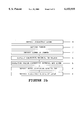
- FIG. 2c is a block diagram showing the steps for producing the structure of FIG. 1c;
- the structure 10b of the present invention comprises substrate 12, overlaid by dielectric layer 14.
- Trench 18 is lined with conductive liner 20 and filled with conductive material 22.
- Conductive metal diffusion barrier cap 24 covers conductive material 22.
- a dielectric etch-stop layer 26 covers dielectric layer 14, conductive material 20, and conductive metal diffusion barrier cap 24.
- a via which extends completely to substrate 12 so that conductive material deposited in the trench 18 is in electrical contact with the underlying layer, may be formed.
- a separate masking step is performed to pattern a square or small rectangular opening (as viewed from above), which may coincide with part of the interconnect trench 18. The opening is etched downward to the underlying level or substrate 12 to form a via.
Abstract
Description
Claims (22)
Priority Applications (3)
| Application Number | Priority Date | Filing Date | Title |
|---|---|---|---|
| US09/409,244 US6153935A (en) | 1999-09-30 | 1999-09-30 | Dual etch stop/diffusion barrier for damascene interconnects |
| US09/641,834 US6358832B1 (en) | 1999-09-30 | 2000-08-18 | Method of forming barrier layers for damascene interconnects |
| KR10-2000-0054915A KR100386155B1 (en) | 1999-09-30 | 2000-09-19 | Dual etch stop/diffusion barrier for damascene interconnects |
Applications Claiming Priority (1)
| Application Number | Priority Date | Filing Date | Title |
|---|---|---|---|
| US09/409,244 US6153935A (en) | 1999-09-30 | 1999-09-30 | Dual etch stop/diffusion barrier for damascene interconnects |
Related Child Applications (1)
| Application Number | Title | Priority Date | Filing Date |
|---|---|---|---|
| US09/641,834 Division US6358832B1 (en) | 1999-09-30 | 2000-08-18 | Method of forming barrier layers for damascene interconnects |
Publications (1)
| Publication Number | Publication Date |
|---|---|
| US6153935A true US6153935A (en) | 2000-11-28 |
Family
ID=23619679
Family Applications (2)
| Application Number | Title | Priority Date | Filing Date |
|---|---|---|---|
| US09/409,244 Expired - Lifetime US6153935A (en) | 1999-09-30 | 1999-09-30 | Dual etch stop/diffusion barrier for damascene interconnects |
| US09/641,834 Expired - Lifetime US6358832B1 (en) | 1999-09-30 | 2000-08-18 | Method of forming barrier layers for damascene interconnects |
Family Applications After (1)
| Application Number | Title | Priority Date | Filing Date |
|---|---|---|---|
| US09/641,834 Expired - Lifetime US6358832B1 (en) | 1999-09-30 | 2000-08-18 | Method of forming barrier layers for damascene interconnects |
Country Status (2)
| Country | Link |
|---|---|
| US (2) | US6153935A (en) |
| KR (1) | KR100386155B1 (en) |
Cited By (239)
| Publication number | Priority date | Publication date | Assignee | Title |
|---|---|---|---|---|
| US6297146B1 (en) * | 1998-10-05 | 2001-10-02 | Advanced Micro Devices, Inc. | Low resistivity semiconductor barrier layer manufacturing method |
| US20020001778A1 (en) * | 2000-06-08 | 2002-01-03 | Applied Materials, Inc. | Photolithography scheme using a silicon containing resist |
| US6342448B1 (en) * | 2000-05-31 | 2002-01-29 | Taiwan Semiconductor Manufacturing Company | Method of fabricating barrier adhesion to low-k dielectric layers in a copper damascene process |
| US6348736B1 (en) * | 1999-10-29 | 2002-02-19 | International Business Machines Corporation | In situ formation of protective layer on silsesquioxane dielectric for dual damascene process |
| US6400030B1 (en) * | 1998-06-12 | 2002-06-04 | Advanced Micro Devices, Inc. | Self-aligning vias for semiconductors |
| US6413869B1 (en) * | 2000-11-06 | 2002-07-02 | Advanced Micro Devices, Inc. | Dielectric protected chemical-mechanical polishing in integrated circuit interconnects |
| US6436778B1 (en) * | 2001-06-12 | 2002-08-20 | Advanced Micro Devices, Inc. | Re-oxidation approach to improve peripheral gate oxide integrity in a tunnel nitride oxidation process |
| US6471884B1 (en) * | 2000-04-04 | 2002-10-29 | Cabot Microelectronics Corporation | Method for polishing a memory or rigid disk with an amino acid-containing composition |
| US20020160222A1 (en) * | 2001-02-28 | 2002-10-31 | Man Hau-Chung | Cobalt-tungsten-phosphorus alloy diffusion barrier coatings, methods for their preparation, and their use in plated articles |
| US6479898B1 (en) * | 2001-01-11 | 2002-11-12 | Advanced Micro Devices, Inc. | Dielectric treatment in integrated circuit interconnects |
| US20030024902A1 (en) * | 2001-03-30 | 2003-02-06 | Li Si Yi | Method of plasma etching low-k dielectric materials |
| US6518641B2 (en) | 2001-05-18 | 2003-02-11 | International Business Machines Corporation | Deep slit isolation with controlled void |
| US6528180B1 (en) * | 2000-05-23 | 2003-03-04 | Applied Materials, Inc. | Liner materials |
| US6541397B1 (en) | 2002-03-29 | 2003-04-01 | Applied Materials, Inc. | Removable amorphous carbon CMP stop |
| US6573030B1 (en) | 2000-02-17 | 2003-06-03 | Applied Materials, Inc. | Method for depositing an amorphous carbon layer |
| US6586328B1 (en) * | 2000-06-05 | 2003-07-01 | The Board Of Trustees Of The University Of Illinois | Method to metallize ohmic electrodes to P-type group III nitrides |
| US20030124255A1 (en) * | 2001-05-28 | 2003-07-03 | Nec Corporation | ULSI wiring and method of manufacturing the same |
| US20030143857A1 (en) * | 2001-03-27 | 2003-07-31 | Micron Technology, Inc. | Post-planarization clean-up |
| US20030190426A1 (en) * | 2002-04-03 | 2003-10-09 | Deenesh Padhi | Electroless deposition method |
| US20030189026A1 (en) * | 2002-04-03 | 2003-10-09 | Deenesh Padhi | Electroless deposition method |
| US20030190812A1 (en) * | 2002-04-03 | 2003-10-09 | Deenesh Padhi | Electroless deposition method |
| US20030199170A1 (en) * | 2001-03-30 | 2003-10-23 | Li Si Yi | Plasma etching of silicon carbide |
| US20030207561A1 (en) * | 2002-05-03 | 2003-11-06 | Dubin Valery M. | Interconnect structures containing conductive electrolessly deposited etch stop layers, liner layers, and via plugs |
| US6657305B1 (en) * | 2000-11-01 | 2003-12-02 | International Business Machines Corporation | Semiconductor recessed mask interconnect technology |
| US6670278B2 (en) | 2001-03-30 | 2003-12-30 | Lam Research Corporation | Method of plasma etching of silicon carbide |
| US6680540B2 (en) | 2000-03-08 | 2004-01-20 | Hitachi, Ltd. | Semiconductor device having cobalt alloy film with boron |
| US6696758B2 (en) | 2000-12-28 | 2004-02-24 | Intel Corporation | Interconnect structures and a method of electroless introduction of interconnect structures |
| US20040062861A1 (en) * | 2001-02-07 | 2004-04-01 | Hiroshi Sato | Method of electroless plating and apparatus for electroless plating |
| WO2004031455A2 (en) * | 2002-10-01 | 2004-04-15 | Universtiy Of Florida | Method, composition and apparatus for tunable selectivity during chemical mechanical polishing of metallic structures |
| US20040087141A1 (en) * | 2002-10-30 | 2004-05-06 | Applied Materials, Inc. | Post rinse to improve selective deposition of electroless cobalt on copper for ULSI application |
| US20040113277A1 (en) * | 2002-12-11 | 2004-06-17 | Chiras Stefanie Ruth | Formation of aligned capped metal lines and interconnections in multilevel semiconductor structures |
| US6753260B1 (en) * | 2001-10-05 | 2004-06-22 | Taiwan Semiconductor Manufacturing Company | Composite etching stop in semiconductor process integration |
| US20040126548A1 (en) * | 2001-05-28 | 2004-07-01 | Waseda University | ULSI wiring and method of manufacturing the same |
| US20040137153A1 (en) * | 2002-04-16 | 2004-07-15 | Michael Thomas | Layered stacks and methods of production thereof |
| US20040180546A1 (en) * | 2003-03-11 | 2004-09-16 | United Microelectronics Corp. | Polish method for semiconductor device planarization |
| US20040265501A1 (en) * | 2003-06-26 | 2004-12-30 | Intel Corporation | Preparation of electroless deposition solutions |
| US6841466B1 (en) | 2003-09-26 | 2005-01-11 | Taiwan Semiconductor Manufacturing Company | Method of selectively making copper using plating technology |
| US20050022745A1 (en) * | 2003-07-30 | 2005-02-03 | Hitachi, Ltd. | Electroless plating method, electroless plating device, and production method and production device of semiconductor device |
| US20050081785A1 (en) * | 2003-10-15 | 2005-04-21 | Applied Materials, Inc. | Apparatus for electroless deposition |
| US20050158666A1 (en) * | 1999-10-15 | 2005-07-21 | Taiwan Semiconductor Manufacturing Company, Ltd. | Lateral etch inhibited multiple etch method for etching material etchable with oxygen containing plasma |
| US20050160575A1 (en) * | 2004-01-22 | 2005-07-28 | International Business Machines Corporation | Integration of high performance copper inductors with bond pads |
| US20050199585A1 (en) * | 2004-03-12 | 2005-09-15 | Applied Materials, Inc. | Method of depositing an amorphous carbon film for metal etch hardmask application |
| US20050199013A1 (en) * | 2004-03-12 | 2005-09-15 | Applied Materials, Inc. | Use of amorphous carbon film as a hardmask in the fabrication of optical waveguides |
| US20050202683A1 (en) * | 2004-03-12 | 2005-09-15 | Applied Materials, Inc. | Method of depositing an amorphous carbon film for etch hardmask application |
| US20050230263A1 (en) * | 2002-12-05 | 2005-10-20 | Dubin Valery M | Methods for forming interconnect structures by co-plating of noble metals and structures formed thereby |
| US20050275100A1 (en) * | 2004-06-14 | 2005-12-15 | Enthone Inc. | Capping of metal interconnects in integrated circuit electronic devices |
| US20050287771A1 (en) * | 2004-03-05 | 2005-12-29 | Applied Materials, Inc. | Liquid precursors for the CVD deposition of amorphous carbon films |
| US20060105558A1 (en) * | 2004-11-18 | 2006-05-18 | Harry Chuang | Inter-metal dielectric scheme for semiconductors |
| US7064065B2 (en) | 2003-10-15 | 2006-06-20 | Applied Materials, Inc. | Silver under-layers for electroless cobalt alloys |
| US20060134911A1 (en) * | 2004-12-22 | 2006-06-22 | Restaino Darryl D | MANUFACTURABLE CoWP METAL CAP PROCESS FOR COPPER INTERCONNECTS |
| US20060165892A1 (en) * | 2005-01-27 | 2006-07-27 | Applied Materials, Inc. | Ruthenium containing layer deposition method |
| US7084070B1 (en) | 2001-03-30 | 2006-08-01 | Lam Research Corporation | Treatment for corrosion in substrate processing |
| US20060216932A1 (en) * | 2005-02-22 | 2006-09-28 | Devendra Kumar | Plasma pre-treating surfaces for atomic layer deposition |
| US20070080455A1 (en) * | 2005-10-11 | 2007-04-12 | International Business Machines Corporation | Semiconductors and methods of making |
| US7205233B2 (en) | 2003-11-07 | 2007-04-17 | Applied Materials, Inc. | Method for forming CoWRe alloys by electroless deposition |
| US20070111519A1 (en) * | 2003-10-15 | 2007-05-17 | Applied Materials, Inc. | Integrated electroless deposition system |
| US20070151951A1 (en) * | 2002-12-06 | 2007-07-05 | Jsr Corporation | Stopper for chemical mechanical planarization, method for manufacturing same, and chemical mechanical planarization method |
| US20070166992A1 (en) * | 2006-01-18 | 2007-07-19 | International Business Machines Corporation | Method for fabricating last level copper-to-c4 connection with interfacial cap structure |
| FR2898906A1 (en) * | 2006-03-21 | 2007-09-28 | Kemesys | Mechanochemical polishing composition useful to polish layers applied on semiconductor microcomponent substrates, comprises alkylxanthate, abrasive particles, metal oxidizing agent, chemical agent to attack metals, pH regulator and solvent |
| US20070286954A1 (en) * | 2006-06-13 | 2007-12-13 | Applied Materials, Inc. | Methods for low temperature deposition of an amorphous carbon layer |
| US20080079154A1 (en) * | 2006-09-29 | 2008-04-03 | Waseda University | Laminated structure, very-large-scale integrated circuit wiring board, and method of formation thereof |
| JP2008510314A (en) * | 2004-08-19 | 2008-04-03 | インテル・コーポレーション | Integrated low-k hard mask |
| US20080179280A1 (en) * | 2007-01-31 | 2008-07-31 | International Business Machines Corporation | Method for forming an indium cap layer |
| US7419903B2 (en) | 2000-03-07 | 2008-09-02 | Asm International N.V. | Thin films |
| US20080237053A1 (en) * | 2002-12-04 | 2008-10-02 | International Business Machines Corporation | Structure comprising a barrier layer of a tungsten alloy comprising cobalt and/or nickel |
| US7514353B2 (en) | 2005-03-18 | 2009-04-07 | Applied Materials, Inc. | Contact metallization scheme using a barrier layer over a silicide layer |
| US20090093128A1 (en) * | 2007-10-08 | 2009-04-09 | Martin Jay Seamons | Methods for high temperature deposition of an amorphous carbon layer |
| US7563715B2 (en) | 2005-12-05 | 2009-07-21 | Asm International N.V. | Method of producing thin films |
| US20090269923A1 (en) * | 2008-04-25 | 2009-10-29 | Lee Sang M | Adhesion and electromigration improvement between dielectric and conductive layers |
| US7651934B2 (en) | 2005-03-18 | 2010-01-26 | Applied Materials, Inc. | Process for electroless copper deposition |
| US7654221B2 (en) | 2003-10-06 | 2010-02-02 | Applied Materials, Inc. | Apparatus for electroless deposition of metals onto semiconductor substrates |
| US7660644B2 (en) | 2001-07-27 | 2010-02-09 | Applied Materials, Inc. | Atomic layer deposition apparatus |
| US7659203B2 (en) | 2005-03-18 | 2010-02-09 | Applied Materials, Inc. | Electroless deposition process on a silicon contact |
| US20100052181A1 (en) * | 2008-08-29 | 2010-03-04 | Thomas Werner | Using a cap layer in metallization systems of semiconductor devices as a cmp and etch stop layer |
| WO2010022969A1 (en) * | 2008-08-29 | 2010-03-04 | Advanced Micro Devices, Inc. | Using a cap layer in metallization systems of semiconductor devices as a cmp and etch stop layer |
| US7827930B2 (en) | 2004-01-26 | 2010-11-09 | Applied Materials, Inc. | Apparatus for electroless deposition of metals onto semiconductor substrates |
| US7867900B2 (en) | 2007-09-28 | 2011-01-11 | Applied Materials, Inc. | Aluminum contact integration on cobalt silicide junction |
| US20110108990A1 (en) * | 2009-11-06 | 2011-05-12 | International Business Machines Corporation | Capping of Copper Interconnect Lines in Integrated Circuit Devices |
| US7972977B2 (en) | 2006-10-05 | 2011-07-05 | Asm America, Inc. | ALD of metal silicate films |
| CN103378052A (en) * | 2012-04-20 | 2013-10-30 | 台湾积体电路制造股份有限公司 | Semiconductor devices, methods of manufacture thereof, and methods of forming conductive features |
| US8679982B2 (en) | 2011-08-26 | 2014-03-25 | Applied Materials, Inc. | Selective suppression of dry-etch rate of materials containing both silicon and oxygen |
| US8679983B2 (en) | 2011-09-01 | 2014-03-25 | Applied Materials, Inc. | Selective suppression of dry-etch rate of materials containing both silicon and nitrogen |
| US8765574B2 (en) | 2012-11-09 | 2014-07-01 | Applied Materials, Inc. | Dry etch process |
| US8771539B2 (en) | 2011-02-22 | 2014-07-08 | Applied Materials, Inc. | Remotely-excited fluorine and water vapor etch |
| US8801952B1 (en) | 2013-03-07 | 2014-08-12 | Applied Materials, Inc. | Conformal oxide dry etch |
| US8808563B2 (en) | 2011-10-07 | 2014-08-19 | Applied Materials, Inc. | Selective etch of silicon by way of metastable hydrogen termination |
| US8846163B2 (en) | 2004-02-26 | 2014-09-30 | Applied Materials, Inc. | Method for removing oxides |
| US8895449B1 (en) | 2013-05-16 | 2014-11-25 | Applied Materials, Inc. | Delicate dry clean |
| US8921234B2 (en) | 2012-12-21 | 2014-12-30 | Applied Materials, Inc. | Selective titanium nitride etching |
| US8927390B2 (en) | 2011-09-26 | 2015-01-06 | Applied Materials, Inc. | Intrench profile |
| US8951429B1 (en) | 2013-10-29 | 2015-02-10 | Applied Materials, Inc. | Tungsten oxide processing |
| US8956980B1 (en) | 2013-09-16 | 2015-02-17 | Applied Materials, Inc. | Selective etch of silicon nitride |
| US8969212B2 (en) | 2012-11-20 | 2015-03-03 | Applied Materials, Inc. | Dry-etch selectivity |
| US8975152B2 (en) | 2011-11-08 | 2015-03-10 | Applied Materials, Inc. | Methods of reducing substrate dislocation during gapfill processing |
| US8980763B2 (en) | 2012-11-30 | 2015-03-17 | Applied Materials, Inc. | Dry-etch for selective tungsten removal |
| US8999856B2 (en) | 2011-03-14 | 2015-04-07 | Applied Materials, Inc. | Methods for etch of sin films |
| US9023734B2 (en) | 2012-09-18 | 2015-05-05 | Applied Materials, Inc. | Radical-component oxide etch |
| US9023732B2 (en) | 2013-03-15 | 2015-05-05 | Applied Materials, Inc. | Processing systems and methods for halide scavenging |
| US9034770B2 (en) | 2012-09-17 | 2015-05-19 | Applied Materials, Inc. | Differential silicon oxide etch |
| US9040422B2 (en) | 2013-03-05 | 2015-05-26 | Applied Materials, Inc. | Selective titanium nitride removal |
| US9064816B2 (en) | 2012-11-30 | 2015-06-23 | Applied Materials, Inc. | Dry-etch for selective oxidation removal |
| US9064815B2 (en) | 2011-03-14 | 2015-06-23 | Applied Materials, Inc. | Methods for etch of metal and metal-oxide films |
| US9111877B2 (en) | 2012-12-18 | 2015-08-18 | Applied Materials, Inc. | Non-local plasma oxide etch |
| US9117855B2 (en) | 2013-12-04 | 2015-08-25 | Applied Materials, Inc. | Polarity control for remote plasma |
| US9114438B2 (en) | 2013-05-21 | 2015-08-25 | Applied Materials, Inc. | Copper residue chamber clean |
| US9136273B1 (en) | 2014-03-21 | 2015-09-15 | Applied Materials, Inc. | Flash gate air gap |
| US9132436B2 (en) | 2012-09-21 | 2015-09-15 | Applied Materials, Inc. | Chemical control features in wafer process equipment |
| US9139906B2 (en) | 2001-03-06 | 2015-09-22 | Asm America, Inc. | Doping with ALD technology |
| US9159606B1 (en) | 2014-07-31 | 2015-10-13 | Applied Materials, Inc. | Metal air gap |
| US9165786B1 (en) | 2014-08-05 | 2015-10-20 | Applied Materials, Inc. | Integrated oxide and nitride recess for better channel contact in 3D architectures |
| US9190293B2 (en) | 2013-12-18 | 2015-11-17 | Applied Materials, Inc. | Even tungsten etch for high aspect ratio trenches |
| US9236265B2 (en) | 2013-11-04 | 2016-01-12 | Applied Materials, Inc. | Silicon germanium processing |
| US9236266B2 (en) | 2011-08-01 | 2016-01-12 | Applied Materials, Inc. | Dry-etch for silicon-and-carbon-containing films |
| US9245762B2 (en) | 2013-12-02 | 2016-01-26 | Applied Materials, Inc. | Procedure for etch rate consistency |
| CN105321930A (en) * | 2014-06-02 | 2016-02-10 | 英飞凌科技股份有限公司 | Vias and methods of formation thereof |
| US9263278B2 (en) | 2013-12-17 | 2016-02-16 | Applied Materials, Inc. | Dopant etch selectivity control |
| US9269590B2 (en) | 2014-04-07 | 2016-02-23 | Applied Materials, Inc. | Spacer formation |
| US9287095B2 (en) | 2013-12-17 | 2016-03-15 | Applied Materials, Inc. | Semiconductor system assemblies and methods of operation |
| US9287134B2 (en) | 2014-01-17 | 2016-03-15 | Applied Materials, Inc. | Titanium oxide etch |
| US9293568B2 (en) | 2014-01-27 | 2016-03-22 | Applied Materials, Inc. | Method of fin patterning |
| US9299537B2 (en) | 2014-03-20 | 2016-03-29 | Applied Materials, Inc. | Radial waveguide systems and methods for post-match control of microwaves |
| US9299582B2 (en) | 2013-11-12 | 2016-03-29 | Applied Materials, Inc. | Selective etch for metal-containing materials |
| US9299575B2 (en) | 2014-03-17 | 2016-03-29 | Applied Materials, Inc. | Gas-phase tungsten etch |
| US9299538B2 (en) | 2014-03-20 | 2016-03-29 | Applied Materials, Inc. | Radial waveguide systems and methods for post-match control of microwaves |
| US9299583B1 (en) | 2014-12-05 | 2016-03-29 | Applied Materials, Inc. | Aluminum oxide selective etch |
| US9309598B2 (en) | 2014-05-28 | 2016-04-12 | Applied Materials, Inc. | Oxide and metal removal |
| US9324576B2 (en) | 2010-05-27 | 2016-04-26 | Applied Materials, Inc. | Selective etch for silicon films |
| US9343272B1 (en) | 2015-01-08 | 2016-05-17 | Applied Materials, Inc. | Self-aligned process |
| US9349605B1 (en) | 2015-08-07 | 2016-05-24 | Applied Materials, Inc. | Oxide etch selectivity systems and methods |
| US9355862B2 (en) | 2014-09-24 | 2016-05-31 | Applied Materials, Inc. | Fluorine-based hardmask removal |
| US9355856B2 (en) | 2014-09-12 | 2016-05-31 | Applied Materials, Inc. | V trench dry etch |
| US9362130B2 (en) | 2013-03-01 | 2016-06-07 | Applied Materials, Inc. | Enhanced etching processes using remote plasma sources |
| US9368364B2 (en) | 2014-09-24 | 2016-06-14 | Applied Materials, Inc. | Silicon etch process with tunable selectivity to SiO2 and other materials |
| US9373517B2 (en) | 2012-08-02 | 2016-06-21 | Applied Materials, Inc. | Semiconductor processing with DC assisted RF power for improved control |
| US9373522B1 (en) | 2015-01-22 | 2016-06-21 | Applied Mateials, Inc. | Titanium nitride removal |
| US9378978B2 (en) | 2014-07-31 | 2016-06-28 | Applied Materials, Inc. | Integrated oxide recess and floating gate fin trimming |
| US9378969B2 (en) | 2014-06-19 | 2016-06-28 | Applied Materials, Inc. | Low temperature gas-phase carbon removal |
| US9385028B2 (en) | 2014-02-03 | 2016-07-05 | Applied Materials, Inc. | Air gap process |
| US9390937B2 (en) | 2012-09-20 | 2016-07-12 | Applied Materials, Inc. | Silicon-carbon-nitride selective etch |
| US9396989B2 (en) | 2014-01-27 | 2016-07-19 | Applied Materials, Inc. | Air gaps between copper lines |
| US9406523B2 (en) | 2014-06-19 | 2016-08-02 | Applied Materials, Inc. | Highly selective doped oxide removal method |
| US9425058B2 (en) | 2014-07-24 | 2016-08-23 | Applied Materials, Inc. | Simplified litho-etch-litho-etch process |
| US9449846B2 (en) | 2015-01-28 | 2016-09-20 | Applied Materials, Inc. | Vertical gate separation |
| US9478432B2 (en) | 2014-09-25 | 2016-10-25 | Applied Materials, Inc. | Silicon oxide selective removal |
| US9496167B2 (en) | 2014-07-31 | 2016-11-15 | Applied Materials, Inc. | Integrated bit-line airgap formation and gate stack post clean |
| US9493879B2 (en) | 2013-07-12 | 2016-11-15 | Applied Materials, Inc. | Selective sputtering for pattern transfer |
| US9499898B2 (en) | 2014-03-03 | 2016-11-22 | Applied Materials, Inc. | Layered thin film heater and method of fabrication |
| US9502258B2 (en) | 2014-12-23 | 2016-11-22 | Applied Materials, Inc. | Anisotropic gap etch |
| US9553102B2 (en) | 2014-08-19 | 2017-01-24 | Applied Materials, Inc. | Tungsten separation |
| US9576809B2 (en) | 2013-11-04 | 2017-02-21 | Applied Materials, Inc. | Etch suppression with germanium |
| US9653327B2 (en) | 2011-05-12 | 2017-05-16 | Applied Materials, Inc. | Methods of removing a material layer from a substrate using water vapor treatment |
| US9659753B2 (en) | 2014-08-07 | 2017-05-23 | Applied Materials, Inc. | Grooved insulator to reduce leakage current |
| US9691645B2 (en) | 2015-08-06 | 2017-06-27 | Applied Materials, Inc. | Bolted wafer chuck thermal management systems and methods for wafer processing systems |
| US9721789B1 (en) | 2016-10-04 | 2017-08-01 | Applied Materials, Inc. | Saving ion-damaged spacers |
| US9728437B2 (en) | 2015-02-03 | 2017-08-08 | Applied Materials, Inc. | High temperature chuck for plasma processing systems |
| US9741593B2 (en) | 2015-08-06 | 2017-08-22 | Applied Materials, Inc. | Thermal management systems and methods for wafer processing systems |
| US9768034B1 (en) | 2016-11-11 | 2017-09-19 | Applied Materials, Inc. | Removal methods for high aspect ratio structures |
| US9773648B2 (en) | 2013-08-30 | 2017-09-26 | Applied Materials, Inc. | Dual discharge modes operation for remote plasma |
| US9847289B2 (en) | 2014-05-30 | 2017-12-19 | Applied Materials, Inc. | Protective via cap for improved interconnect performance |
| US9865484B1 (en) | 2016-06-29 | 2018-01-09 | Applied Materials, Inc. | Selective etch using material modification and RF pulsing |
| US9881805B2 (en) | 2015-03-02 | 2018-01-30 | Applied Materials, Inc. | Silicon selective removal |
| US9885117B2 (en) | 2014-03-31 | 2018-02-06 | Applied Materials, Inc. | Conditioned semiconductor system parts |
| US9934942B1 (en) | 2016-10-04 | 2018-04-03 | Applied Materials, Inc. | Chamber with flow-through source |
| US9947549B1 (en) | 2016-10-10 | 2018-04-17 | Applied Materials, Inc. | Cobalt-containing material removal |
| US10026621B2 (en) | 2016-11-14 | 2018-07-17 | Applied Materials, Inc. | SiN spacer profile patterning |
| US10043674B1 (en) | 2017-08-04 | 2018-08-07 | Applied Materials, Inc. | Germanium etching systems and methods |
| US10043684B1 (en) | 2017-02-06 | 2018-08-07 | Applied Materials, Inc. | Self-limiting atomic thermal etching systems and methods |
| US10049891B1 (en) | 2017-05-31 | 2018-08-14 | Applied Materials, Inc. | Selective in situ cobalt residue removal |
| US10062587B2 (en) | 2012-07-18 | 2018-08-28 | Applied Materials, Inc. | Pedestal with multi-zone temperature control and multiple purge capabilities |
| US10062575B2 (en) | 2016-09-09 | 2018-08-28 | Applied Materials, Inc. | Poly directional etch by oxidation |
| US10062585B2 (en) | 2016-10-04 | 2018-08-28 | Applied Materials, Inc. | Oxygen compatible plasma source |
| US10062579B2 (en) | 2016-10-07 | 2018-08-28 | Applied Materials, Inc. | Selective SiN lateral recess |
| US10128086B1 (en) | 2017-10-24 | 2018-11-13 | Applied Materials, Inc. | Silicon pretreatment for nitride removal |
| US10163696B2 (en) | 2016-11-11 | 2018-12-25 | Applied Materials, Inc. | Selective cobalt removal for bottom up gapfill |
| US10170336B1 (en) | 2017-08-04 | 2019-01-01 | Applied Materials, Inc. | Methods for anisotropic control of selective silicon removal |
| US10170282B2 (en) | 2013-03-08 | 2019-01-01 | Applied Materials, Inc. | Insulated semiconductor faceplate designs |
| US10224210B2 (en) | 2014-12-09 | 2019-03-05 | Applied Materials, Inc. | Plasma processing system with direct outlet toroidal plasma source |
| US10242908B2 (en) | 2016-11-14 | 2019-03-26 | Applied Materials, Inc. | Airgap formation with damage-free copper |
| US10256112B1 (en) | 2017-12-08 | 2019-04-09 | Applied Materials, Inc. | Selective tungsten removal |
| US10256079B2 (en) | 2013-02-08 | 2019-04-09 | Applied Materials, Inc. | Semiconductor processing systems having multiple plasma configurations |
| US10283321B2 (en) | 2011-01-18 | 2019-05-07 | Applied Materials, Inc. | Semiconductor processing system and methods using capacitively coupled plasma |
| US10283324B1 (en) | 2017-10-24 | 2019-05-07 | Applied Materials, Inc. | Oxygen treatment for nitride etching |
| US10297458B2 (en) | 2017-08-07 | 2019-05-21 | Applied Materials, Inc. | Process window widening using coated parts in plasma etch processes |
| US10319649B2 (en) | 2017-04-11 | 2019-06-11 | Applied Materials, Inc. | Optical emission spectroscopy (OES) for remote plasma monitoring |
| US10319600B1 (en) | 2018-03-12 | 2019-06-11 | Applied Materials, Inc. | Thermal silicon etch |
| US10319739B2 (en) | 2017-02-08 | 2019-06-11 | Applied Materials, Inc. | Accommodating imperfectly aligned memory holes |
| US10354889B2 (en) | 2017-07-17 | 2019-07-16 | Applied Materials, Inc. | Non-halogen etching of silicon-containing materials |
| US10403507B2 (en) | 2017-02-03 | 2019-09-03 | Applied Materials, Inc. | Shaped etch profile with oxidation |
| US10431429B2 (en) | 2017-02-03 | 2019-10-01 | Applied Materials, Inc. | Systems and methods for radial and azimuthal control of plasma uniformity |
| US10468267B2 (en) | 2017-05-31 | 2019-11-05 | Applied Materials, Inc. | Water-free etching methods |
| US10490418B2 (en) | 2014-10-14 | 2019-11-26 | Applied Materials, Inc. | Systems and methods for internal surface conditioning assessment in plasma processing equipment |
| US10490406B2 (en) | 2018-04-10 | 2019-11-26 | Appled Materials, Inc. | Systems and methods for material breakthrough |
| US10497573B2 (en) | 2018-03-13 | 2019-12-03 | Applied Materials, Inc. | Selective atomic layer etching of semiconductor materials |
| US10504754B2 (en) | 2016-05-19 | 2019-12-10 | Applied Materials, Inc. | Systems and methods for improved semiconductor etching and component protection |
| US10504700B2 (en) | 2015-08-27 | 2019-12-10 | Applied Materials, Inc. | Plasma etching systems and methods with secondary plasma injection |
| US10522371B2 (en) | 2016-05-19 | 2019-12-31 | Applied Materials, Inc. | Systems and methods for improved semiconductor etching and component protection |
| US10541246B2 (en) | 2017-06-26 | 2020-01-21 | Applied Materials, Inc. | 3D flash memory cells which discourage cross-cell electrical tunneling |
| US10541184B2 (en) | 2017-07-11 | 2020-01-21 | Applied Materials, Inc. | Optical emission spectroscopic techniques for monitoring etching |
| US10546729B2 (en) | 2016-10-04 | 2020-01-28 | Applied Materials, Inc. | Dual-channel showerhead with improved profile |
| US10566206B2 (en) | 2016-12-27 | 2020-02-18 | Applied Materials, Inc. | Systems and methods for anisotropic material breakthrough |
| US10573527B2 (en) | 2018-04-06 | 2020-02-25 | Applied Materials, Inc. | Gas-phase selective etching systems and methods |
| US10573496B2 (en) | 2014-12-09 | 2020-02-25 | Applied Materials, Inc. | Direct outlet toroidal plasma source |
| US10593523B2 (en) | 2014-10-14 | 2020-03-17 | Applied Materials, Inc. | Systems and methods for internal surface conditioning in plasma processing equipment |
| US10593560B2 (en) | 2018-03-01 | 2020-03-17 | Applied Materials, Inc. | Magnetic induction plasma source for semiconductor processes and equipment |
| US10615047B2 (en) | 2018-02-28 | 2020-04-07 | Applied Materials, Inc. | Systems and methods to form airgaps |
| US10629473B2 (en) | 2016-09-09 | 2020-04-21 | Applied Materials, Inc. | Footing removal for nitride spacer |
| US10672642B2 (en) | 2018-07-24 | 2020-06-02 | Applied Materials, Inc. | Systems and methods for pedestal configuration |
| US10679870B2 (en) | 2018-02-15 | 2020-06-09 | Applied Materials, Inc. | Semiconductor processing chamber multistage mixing apparatus |
| US10699879B2 (en) | 2018-04-17 | 2020-06-30 | Applied Materials, Inc. | Two piece electrode assembly with gap for plasma control |
| US10727080B2 (en) | 2017-07-07 | 2020-07-28 | Applied Materials, Inc. | Tantalum-containing material removal |
| US10755941B2 (en) | 2018-07-06 | 2020-08-25 | Applied Materials, Inc. | Self-limiting selective etching systems and methods |
| US10854426B2 (en) | 2018-01-08 | 2020-12-01 | Applied Materials, Inc. | Metal recess for semiconductor structures |
| US10872778B2 (en) | 2018-07-06 | 2020-12-22 | Applied Materials, Inc. | Systems and methods utilizing solid-phase etchants |
| US10886137B2 (en) | 2018-04-30 | 2021-01-05 | Applied Materials, Inc. | Selective nitride removal |
| US10892198B2 (en) | 2018-09-14 | 2021-01-12 | Applied Materials, Inc. | Systems and methods for improved performance in semiconductor processing |
| US10903054B2 (en) | 2017-12-19 | 2021-01-26 | Applied Materials, Inc. | Multi-zone gas distribution systems and methods |
| US10920320B2 (en) | 2017-06-16 | 2021-02-16 | Applied Materials, Inc. | Plasma health determination in semiconductor substrate processing reactors |
| US10920319B2 (en) | 2019-01-11 | 2021-02-16 | Applied Materials, Inc. | Ceramic showerheads with conductive electrodes |
| US10943834B2 (en) | 2017-03-13 | 2021-03-09 | Applied Materials, Inc. | Replacement contact process |
| US10964512B2 (en) | 2018-02-15 | 2021-03-30 | Applied Materials, Inc. | Semiconductor processing chamber multistage mixing apparatus and methods |
| US11049755B2 (en) | 2018-09-14 | 2021-06-29 | Applied Materials, Inc. | Semiconductor substrate supports with embedded RF shield |
| US11062887B2 (en) | 2018-09-17 | 2021-07-13 | Applied Materials, Inc. | High temperature RF heater pedestals |
| US11121002B2 (en) | 2018-10-24 | 2021-09-14 | Applied Materials, Inc. | Systems and methods for etching metals and metal derivatives |
| US11145813B2 (en) | 2018-09-24 | 2021-10-12 | International Business Machines Corporation | Bottom electrode for semiconductor memory device |
| US11152299B2 (en) | 2020-03-03 | 2021-10-19 | International Business Machines Corporation | Hybrid selective dielectric deposition for aligned via integration |
| US11217742B2 (en) * | 2018-09-24 | 2022-01-04 | International Business Machines Corporation | Bottom electrode for semiconductor memory device |
| US11239061B2 (en) | 2014-11-26 | 2022-02-01 | Applied Materials, Inc. | Methods and systems to enhance process uniformity |
| US11251368B2 (en) | 2020-04-20 | 2022-02-15 | International Business Machines Corporation | Interconnect structures with selective capping layer |
| US11257693B2 (en) | 2015-01-09 | 2022-02-22 | Applied Materials, Inc. | Methods and systems to improve pedestal temperature control |
| US11276590B2 (en) | 2017-05-17 | 2022-03-15 | Applied Materials, Inc. | Multi-zone semiconductor substrate supports |
| US11276559B2 (en) | 2017-05-17 | 2022-03-15 | Applied Materials, Inc. | Semiconductor processing chamber for multiple precursor flow |
| US11328909B2 (en) | 2017-12-22 | 2022-05-10 | Applied Materials, Inc. | Chamber conditioning and removal processes |
| US11342221B2 (en) | 2019-09-04 | 2022-05-24 | Samsung Electronics Co., Ltd. | Semiconductor device |
| US11417534B2 (en) | 2018-09-21 | 2022-08-16 | Applied Materials, Inc. | Selective material removal |
| US11437242B2 (en) | 2018-11-27 | 2022-09-06 | Applied Materials, Inc. | Selective removal of silicon-containing materials |
| US11594428B2 (en) | 2015-02-03 | 2023-02-28 | Applied Materials, Inc. | Low temperature chuck for plasma processing systems |
| US11682560B2 (en) | 2018-10-11 | 2023-06-20 | Applied Materials, Inc. | Systems and methods for hafnium-containing film removal |
| US11721527B2 (en) | 2019-01-07 | 2023-08-08 | Applied Materials, Inc. | Processing chamber mixing systems |
| US11854878B2 (en) * | 2019-12-27 | 2023-12-26 | Taiwan Semiconductor Manufacturing Ltd. | Bi-layer alloy liner for interconnect metallization and methods of forming the same |
Families Citing this family (49)
| Publication number | Priority date | Publication date | Assignee | Title |
|---|---|---|---|---|
| JP2001319928A (en) * | 2000-05-08 | 2001-11-16 | Hitachi Ltd | Semiconductor integrated circuit device and manufacturing method therefor |
| GB0025989D0 (en) * | 2000-10-24 | 2000-12-13 | Shipley Co Llc | Plating catalysts |
| JP2003077920A (en) * | 2001-09-04 | 2003-03-14 | Nec Corp | Method for forming metal wiring |
| KR100442962B1 (en) * | 2001-12-26 | 2004-08-04 | 주식회사 하이닉스반도체 | Method for manufacturing of metal line contact plug of semiconductor device |
| US6732908B2 (en) * | 2002-01-18 | 2004-05-11 | International Business Machines Corporation | High density raised stud microjoining system and methods of fabricating the same |
| DE10227615A1 (en) * | 2002-06-20 | 2004-01-15 | Infineon Technologies Ag | Layer arrangement and method for producing a layer arrangement |
| US6838354B2 (en) * | 2002-12-20 | 2005-01-04 | Freescale Semiconductor, Inc. | Method for forming a passivation layer for air gap formation |
| US20050064701A1 (en) * | 2003-09-19 | 2005-03-24 | International Business Machines Corporation | Formation of low resistance via contacts in interconnect structures |
| US20050098605A1 (en) * | 2003-11-06 | 2005-05-12 | International Business Machines Corporation | Apparatus and method for low pressure wirebond |
| US7405147B2 (en) * | 2004-01-30 | 2008-07-29 | International Business Machines Corporation | Device and methodology for reducing effective dielectric constant in semiconductor devices |
| JP3910973B2 (en) * | 2004-04-22 | 2007-04-25 | 株式会社東芝 | Manufacturing method of semiconductor device |
| US7223692B2 (en) * | 2004-04-30 | 2007-05-29 | Taiwan Semiconductor Manufacturing Co., Ltd | Multi-level semiconductor device with capping layer for improved adhesion |
| US7390748B2 (en) * | 2004-08-05 | 2008-06-24 | International Business Machines Corporation | Method of forming a polishing inhibiting layer using a slurry having an additive |
| US7422979B2 (en) * | 2005-03-11 | 2008-09-09 | Freescale Semiconductor, Inc. | Method of forming a semiconductor device having a diffusion barrier stack and structure thereof |
| US7402519B2 (en) * | 2005-06-03 | 2008-07-22 | Intel Corporation | Interconnects having sealing structures to enable selective metal capping layers |
| US7521355B2 (en) * | 2005-12-08 | 2009-04-21 | Micron Technology, Inc. | Integrated circuit insulators and related methods |
| US8193087B2 (en) * | 2006-05-18 | 2012-06-05 | Taiwan Semiconductor Manufacturing Co., Ltd. | Process for improving copper line cap formation |
| US20070296083A1 (en) * | 2006-06-21 | 2007-12-27 | Micron Technology, Inc. | Low dielectric constant integrated circuit insulators and methods |
| KR100835422B1 (en) | 2006-12-27 | 2008-06-04 | 동부일렉트로닉스 주식회사 | Method for forming metal line of semiconductor device |
| JP5154140B2 (en) * | 2006-12-28 | 2013-02-27 | 東京エレクトロン株式会社 | Semiconductor device and manufacturing method thereof |
| EP2125985B1 (en) * | 2006-12-29 | 2012-08-15 | LG Chem, Ltd. | Cmp slurry composition for forming metal wiring line |
| US7666753B2 (en) * | 2007-01-11 | 2010-02-23 | International Business Machines Corporation | Metal capping process for BEOL interconnect with air gaps |
| US7544609B2 (en) * | 2007-02-09 | 2009-06-09 | International Business Machines Corporation | Method for integrating liner formation in back end of line processing |
| US20080258303A1 (en) * | 2007-04-23 | 2008-10-23 | Ming-Shih Yeh | Novel structure for reducing low-k dielectric damage and improving copper EM performance |
| US7514361B2 (en) * | 2007-08-20 | 2009-04-07 | International Business Machines Corporation | Selective thin metal cap process |
| US7905994B2 (en) * | 2007-10-03 | 2011-03-15 | Moses Lake Industries, Inc. | Substrate holder and electroplating system |
| US20090188553A1 (en) * | 2008-01-25 | 2009-07-30 | Emat Technology, Llc | Methods of fabricating solar-cell structures and resulting solar-cell structures |
| US20100084766A1 (en) * | 2008-10-08 | 2010-04-08 | International Business Machines Corporation | Surface repair structure and process for interconnect applications |
| WO2010065457A2 (en) * | 2008-12-02 | 2010-06-10 | Arizona Board Of Regents, For And On Behalf Of Arizona State University | Method of providing a semiconductor device with a dielectric layer and semiconductor device thereof |
| US9601530B2 (en) | 2008-12-02 | 2017-03-21 | Arizona Board Of Regents, A Body Corporated Of The State Of Arizona, Acting For And On Behalf Of Arizona State University | Dual active layer semiconductor device and method of manufacturing the same |
| WO2010065459A2 (en) * | 2008-12-02 | 2010-06-10 | Arizona Board Of Regents, For And On Behalf Of Arizona State University | Method of etching organosiloxane dielectric material and semiconductor device thereof |
| US9991311B2 (en) | 2008-12-02 | 2018-06-05 | Arizona Board Of Regents On Behalf Of Arizona State University | Dual active layer semiconductor device and method of manufacturing the same |
| US9721825B2 (en) | 2008-12-02 | 2017-08-01 | Arizona Board Of Regents, A Body Corporate Of The State Of Arizona, Acting For And On Behalf Of Arizona State University | Method of providing a flexible semiconductor device and flexible semiconductor device thereof |
| US8262894B2 (en) | 2009-04-30 | 2012-09-11 | Moses Lake Industries, Inc. | High speed copper plating bath |
| TW201117262A (en) | 2009-05-29 | 2011-05-16 | Univ Arizona | Method of providing a flexible semiconductor device at high temperatures and flexible semiconductor device thereof |
| WO2012021196A2 (en) | 2010-05-21 | 2012-02-16 | Arizona Board Of Regents, For And On Behalf Of Arizona State University | Method for manufacturing electronic devices and electronic devices thereof |
| WO2012021197A2 (en) | 2010-05-21 | 2012-02-16 | Arizona Board Of Regents, For And On Behalf Of Arizona State University | Method of manufacturing electronic devices on both sides of a carrier substrate and electronic devices thereof |
| US8889544B2 (en) | 2011-02-16 | 2014-11-18 | Taiwan Semiconductor Manufacturing Company, Ltd. | Dielectric protection layer as a chemical-mechanical polishing stop layer |
| US8461683B2 (en) * | 2011-04-01 | 2013-06-11 | Intel Corporation | Self-forming, self-aligned barriers for back-end interconnects and methods of making same |
| US9330989B2 (en) | 2012-09-28 | 2016-05-03 | Taiwan Semiconductor Manufacturing Company, Ltd. | System and method for chemical-mechanical planarization of a metal layer |
| US8802558B2 (en) | 2012-11-07 | 2014-08-12 | International Business Machines Corporation | Copper interconnect structures and methods of making same |
| US8951909B2 (en) * | 2013-03-13 | 2015-02-10 | Taiwan Semiconductor Manufacturing Company Limited | Integrated circuit structure and formation |
| US10381224B2 (en) | 2014-01-23 | 2019-08-13 | Arizona Board Of Regents On Behalf Of Arizona State University | Method of providing an electronic device and electronic device thereof |
| WO2015156891A2 (en) | 2014-01-23 | 2015-10-15 | Arizona Board Of Regents, Acting For And On Behalf Of Arizona State University | Method of providing a flexible semiconductor device and flexible semiconductor device thereof |
| WO2017034644A2 (en) | 2015-06-09 | 2017-03-02 | ARIZONA BOARD OF REGENTS a body corporate for THE STATE OF ARIZONA for and on behalf of ARIZONA STATE UNIVERSITY | Method of providing an electronic device and electronic device thereof |
| CN106663640B (en) | 2014-05-13 | 2020-01-07 | 代表亚利桑那大学的亚利桑那校董会 | Method of providing an electronic device and electronic device thereof |
| US10446582B2 (en) | 2014-12-22 | 2019-10-15 | Arizona Board Of Regents On Behalf Of Arizona State University | Method of providing an imaging system and imaging system thereof |
| US9741742B2 (en) | 2014-12-22 | 2017-08-22 | Arizona Board Of Regents, A Body Corporate Of The State Of Arizona, Acting For And On Behalf Of Arizona State University | Deformable electronic device and methods of providing and using deformable electronic device |
| US10204829B1 (en) | 2018-01-12 | 2019-02-12 | International Business Machines Corporation | Low-resistivity metallic interconnect structures with self-forming diffusion barrier layers |
Citations (3)
| Publication number | Priority date | Publication date | Assignee | Title |
|---|---|---|---|---|
| US5708303A (en) * | 1994-09-15 | 1998-01-13 | Texas Instruments Incorporated | Semiconductor device having damascene interconnects |
| US5817572A (en) * | 1992-06-29 | 1998-10-06 | Intel Corporation | Method for forming multileves interconnections for semiconductor fabrication |
| US6004188A (en) * | 1998-09-10 | 1999-12-21 | Chartered Semiconductor Manufacturing Ltd. | Method for forming copper damascene structures by using a dual CMP barrier layer |
Family Cites Families (13)
| Publication number | Priority date | Publication date | Assignee | Title |
|---|---|---|---|---|
| US4789648A (en) | 1985-10-28 | 1988-12-06 | International Business Machines Corporation | Method for producing coplanar multi-level metal/insulator films on a substrate and for forming patterned conductive lines simultaneously with stud vias |
| US4944836A (en) | 1985-10-28 | 1990-07-31 | International Business Machines Corporation | Chem-mech polishing method for producing coplanar metal/insulator films on a substrate |
| EP0261846B1 (en) | 1986-09-17 | 1992-12-02 | Fujitsu Limited | Method of forming a metallization film containing copper on the surface of a semiconductor device |
| JPH07135188A (en) | 1993-11-11 | 1995-05-23 | Toshiba Corp | Manufacture of semiconductor device |
| US5447887A (en) | 1994-04-01 | 1995-09-05 | Motorola, Inc. | Method for capping copper in semiconductor devices |
| US5736457A (en) | 1994-12-09 | 1998-04-07 | Sematech | Method of making a damascene metallization |
| US5874201A (en) | 1995-06-05 | 1999-02-23 | International Business Machines Corporation | Dual damascene process having tapered vias |
| TW304297B (en) * | 1995-09-29 | 1997-05-01 | Intel Corp | |
| US5714418A (en) | 1995-11-08 | 1998-02-03 | Intel Corporation | Diffusion barrier for electrical interconnects in an integrated circuit |
| US5676587A (en) | 1995-12-06 | 1997-10-14 | International Business Machines Corporation | Selective polish process for titanium, titanium nitride, tantalum and tantalum nitride |
| US5824599A (en) | 1996-01-16 | 1998-10-20 | Cornell Research Foundation, Inc. | Protected encapsulation of catalytic layer for electroless copper interconnect |
| US5744376A (en) | 1996-04-08 | 1998-04-28 | Chartered Semiconductor Manufacturing Pte, Ltd | Method of manufacturing copper interconnect with top barrier layer |
| US6051496A (en) * | 1998-09-17 | 2000-04-18 | Taiwan Semiconductor Manufacturing Company | Use of stop layer for chemical mechanical polishing of CU damascene |
-
1999
- 1999-09-30 US US09/409,244 patent/US6153935A/en not_active Expired - Lifetime
-
2000
- 2000-08-18 US US09/641,834 patent/US6358832B1/en not_active Expired - Lifetime
- 2000-09-19 KR KR10-2000-0054915A patent/KR100386155B1/en not_active IP Right Cessation
Patent Citations (3)
| Publication number | Priority date | Publication date | Assignee | Title |
|---|---|---|---|---|
| US5817572A (en) * | 1992-06-29 | 1998-10-06 | Intel Corporation | Method for forming multileves interconnections for semiconductor fabrication |
| US5708303A (en) * | 1994-09-15 | 1998-01-13 | Texas Instruments Incorporated | Semiconductor device having damascene interconnects |
| US6004188A (en) * | 1998-09-10 | 1999-12-21 | Chartered Semiconductor Manufacturing Ltd. | Method for forming copper damascene structures by using a dual CMP barrier layer |
Cited By (370)
| Publication number | Priority date | Publication date | Assignee | Title |
|---|---|---|---|---|
| US6400030B1 (en) * | 1998-06-12 | 2002-06-04 | Advanced Micro Devices, Inc. | Self-aligning vias for semiconductors |
| US6297146B1 (en) * | 1998-10-05 | 2001-10-02 | Advanced Micro Devices, Inc. | Low resistivity semiconductor barrier layer manufacturing method |
| US20050158666A1 (en) * | 1999-10-15 | 2005-07-21 | Taiwan Semiconductor Manufacturing Company, Ltd. | Lateral etch inhibited multiple etch method for etching material etchable with oxygen containing plasma |
| US6348736B1 (en) * | 1999-10-29 | 2002-02-19 | International Business Machines Corporation | In situ formation of protective layer on silsesquioxane dielectric for dual damascene process |
| US6841341B2 (en) | 2000-02-17 | 2005-01-11 | Applied Materials, Inc. | Method of depositing an amorphous carbon layer |
| US20050233257A1 (en) * | 2000-02-17 | 2005-10-20 | Applied Materials, Inc. | Photolithography scheme using a silicon containing resist |
| US7223526B2 (en) | 2000-02-17 | 2007-05-29 | Applied Materials, Inc. | Method of depositing an amorphous carbon layer |
| US6573030B1 (en) | 2000-02-17 | 2003-06-03 | Applied Materials, Inc. | Method for depositing an amorphous carbon layer |
| US7332262B2 (en) | 2000-02-17 | 2008-02-19 | Applied Materials, Inc. | Photolithography scheme using a silicon containing resist |
| US7335462B2 (en) | 2000-02-17 | 2008-02-26 | Applied Materials, Inc. | Method of depositing an amorphous carbon layer |
| US7981791B2 (en) | 2000-03-07 | 2011-07-19 | Asm International N.V. | Thin films |
| US20090068832A1 (en) * | 2000-03-07 | 2009-03-12 | Asm International N.V. | Thin films |
| US7419903B2 (en) | 2000-03-07 | 2008-09-02 | Asm International N.V. | Thin films |
| US6680540B2 (en) | 2000-03-08 | 2004-01-20 | Hitachi, Ltd. | Semiconductor device having cobalt alloy film with boron |
| US6471884B1 (en) * | 2000-04-04 | 2002-10-29 | Cabot Microelectronics Corporation | Method for polishing a memory or rigid disk with an amino acid-containing composition |
| US6528180B1 (en) * | 2000-05-23 | 2003-03-04 | Applied Materials, Inc. | Liner materials |
| US6342448B1 (en) * | 2000-05-31 | 2002-01-29 | Taiwan Semiconductor Manufacturing Company | Method of fabricating barrier adhesion to low-k dielectric layers in a copper damascene process |
| US6586328B1 (en) * | 2000-06-05 | 2003-07-01 | The Board Of Trustees Of The University Of Illinois | Method to metallize ohmic electrodes to P-type group III nitrides |
| US20020001778A1 (en) * | 2000-06-08 | 2002-01-03 | Applied Materials, Inc. | Photolithography scheme using a silicon containing resist |
| US6967072B2 (en) | 2000-06-08 | 2005-11-22 | Applied Materials, Inc. | Photolithography scheme using a silicon containing resist |
| US6657305B1 (en) * | 2000-11-01 | 2003-12-02 | International Business Machines Corporation | Semiconductor recessed mask interconnect technology |
| US20040051178A1 (en) * | 2000-11-01 | 2004-03-18 | International Business Machines Corporation | Semiconductor recessed mask interconnect technology |
| US6413869B1 (en) * | 2000-11-06 | 2002-07-02 | Advanced Micro Devices, Inc. | Dielectric protected chemical-mechanical polishing in integrated circuit interconnects |
| US6977224B2 (en) | 2000-12-28 | 2005-12-20 | Intel Corporation | Method of electroless introduction of interconnect structures |
| US6696758B2 (en) | 2000-12-28 | 2004-02-24 | Intel Corporation | Interconnect structures and a method of electroless introduction of interconnect structures |
| US6479898B1 (en) * | 2001-01-11 | 2002-11-12 | Advanced Micro Devices, Inc. | Dielectric treatment in integrated circuit interconnects |
| US20040062861A1 (en) * | 2001-02-07 | 2004-04-01 | Hiroshi Sato | Method of electroless plating and apparatus for electroless plating |
| US6528185B2 (en) * | 2001-02-28 | 2003-03-04 | Hong Kong Polytechnic University | Cobalt-tungsten-phosphorus alloy diffusion barrier coatings, methods for their preparation, and their use in plated articles |
| US20020160222A1 (en) * | 2001-02-28 | 2002-10-31 | Man Hau-Chung | Cobalt-tungsten-phosphorus alloy diffusion barrier coatings, methods for their preparation, and their use in plated articles |
| US9139906B2 (en) | 2001-03-06 | 2015-09-22 | Asm America, Inc. | Doping with ALD technology |
| US7033978B2 (en) | 2001-03-27 | 2006-04-25 | Micron Technology, Inc. | Post-planarization clean-up |
| US20030143857A1 (en) * | 2001-03-27 | 2003-07-31 | Micron Technology, Inc. | Post-planarization clean-up |
| US6787473B2 (en) | 2001-03-27 | 2004-09-07 | Micron Technology, Inc. | Post-planarization clean-up |
| US6627550B2 (en) | 2001-03-27 | 2003-09-30 | Micron Technology, Inc. | Post-planarization clean-up |
| US7084070B1 (en) | 2001-03-30 | 2006-08-01 | Lam Research Corporation | Treatment for corrosion in substrate processing |
| US6670278B2 (en) | 2001-03-30 | 2003-12-30 | Lam Research Corporation | Method of plasma etching of silicon carbide |
| US7311852B2 (en) | 2001-03-30 | 2007-12-25 | Lam Research Corporation | Method of plasma etching low-k dielectric materials |
| US6919278B2 (en) | 2001-03-30 | 2005-07-19 | Lam Research Corporation | Method for etching silicon carbide |
| US7166535B2 (en) | 2001-03-30 | 2007-01-23 | Lam Research Corporation | Plasma etching of silicon carbide |
| US20030024902A1 (en) * | 2001-03-30 | 2003-02-06 | Li Si Yi | Method of plasma etching low-k dielectric materials |
| US20030199170A1 (en) * | 2001-03-30 | 2003-10-23 | Li Si Yi | Plasma etching of silicon carbide |
| US6518641B2 (en) | 2001-05-18 | 2003-02-11 | International Business Machines Corporation | Deep slit isolation with controlled void |
| US20040126548A1 (en) * | 2001-05-28 | 2004-07-01 | Waseda University | ULSI wiring and method of manufacturing the same |
| US20030124255A1 (en) * | 2001-05-28 | 2003-07-03 | Nec Corporation | ULSI wiring and method of manufacturing the same |
| US20100006326A1 (en) * | 2001-05-28 | 2010-01-14 | Nec Electronics Corporation | Ulsi wiring and method of manufacturing the same |
| US8784931B2 (en) | 2001-05-28 | 2014-07-22 | Waseda University | ULSI wiring and method of manufacturing the same |
| US6436778B1 (en) * | 2001-06-12 | 2002-08-20 | Advanced Micro Devices, Inc. | Re-oxidation approach to improve peripheral gate oxide integrity in a tunnel nitride oxidation process |
| US7660644B2 (en) | 2001-07-27 | 2010-02-09 | Applied Materials, Inc. | Atomic layer deposition apparatus |
| US9031685B2 (en) | 2001-07-27 | 2015-05-12 | Applied Materials, Inc. | Atomic layer deposition apparatus |
| US7860597B2 (en) | 2001-07-27 | 2010-12-28 | Applied Materials, Inc. | Atomic layer deposition apparatus |
| US8626330B2 (en) | 2001-07-27 | 2014-01-07 | Applied Materials, Inc. | Atomic layer deposition apparatus |
| US8027746B2 (en) | 2001-07-27 | 2011-09-27 | Applied Materials, Inc. | Atomic layer deposition apparatus |
| US6753260B1 (en) * | 2001-10-05 | 2004-06-22 | Taiwan Semiconductor Manufacturing Company | Composite etching stop in semiconductor process integration |
| US7507677B2 (en) | 2002-03-29 | 2009-03-24 | Applied Materials, Inc. | Removable amorphous carbon CMP stop |
| US6541397B1 (en) | 2002-03-29 | 2003-04-01 | Applied Materials, Inc. | Removable amorphous carbon CMP stop |
| US20030186477A1 (en) * | 2002-03-29 | 2003-10-02 | Applied Materials, Inc. | Removable amorphous carbon CMP stop |
| US6852647B2 (en) | 2002-03-29 | 2005-02-08 | Applied Materials, Inc. | Removable amorphous carbon CMP stop |
| US7148156B2 (en) | 2002-03-29 | 2006-12-12 | Applied Materials, Inc. | Removable amorphous carbon CMP stop |
| US6905622B2 (en) | 2002-04-03 | 2005-06-14 | Applied Materials, Inc. | Electroless deposition method |
| US20030190812A1 (en) * | 2002-04-03 | 2003-10-09 | Deenesh Padhi | Electroless deposition method |
| US20030190426A1 (en) * | 2002-04-03 | 2003-10-09 | Deenesh Padhi | Electroless deposition method |
| US20030189026A1 (en) * | 2002-04-03 | 2003-10-09 | Deenesh Padhi | Electroless deposition method |
| US6899816B2 (en) | 2002-04-03 | 2005-05-31 | Applied Materials, Inc. | Electroless deposition method |
| US20040137153A1 (en) * | 2002-04-16 | 2004-07-15 | Michael Thomas | Layered stacks and methods of production thereof |
| US7008872B2 (en) | 2002-05-03 | 2006-03-07 | Intel Corporation | Use of conductive electrolessly deposited etch stop layers, liner layers and via plugs in interconnect structures |
| US6958547B2 (en) | 2002-05-03 | 2005-10-25 | Intel Corporation | Interconnect structures containing conductive electrolessly deposited etch stop layers, liner layers, and via plugs |
| US20030207561A1 (en) * | 2002-05-03 | 2003-11-06 | Dubin Valery M. | Interconnect structures containing conductive electrolessly deposited etch stop layers, liner layers, and via plugs |
| WO2004031455A3 (en) * | 2002-10-01 | 2005-11-03 | Universtiy Of Florida | Method, composition and apparatus for tunable selectivity during chemical mechanical polishing of metallic structures |
| WO2004031455A2 (en) * | 2002-10-01 | 2004-04-15 | Universtiy Of Florida | Method, composition and apparatus for tunable selectivity during chemical mechanical polishing of metallic structures |
| US20040087141A1 (en) * | 2002-10-30 | 2004-05-06 | Applied Materials, Inc. | Post rinse to improve selective deposition of electroless cobalt on copper for ULSI application |
| US6821909B2 (en) | 2002-10-30 | 2004-11-23 | Applied Materials, Inc. | Post rinse to improve selective deposition of electroless cobalt on copper for ULSI application |
| US20080237053A1 (en) * | 2002-12-04 | 2008-10-02 | International Business Machines Corporation | Structure comprising a barrier layer of a tungsten alloy comprising cobalt and/or nickel |
| US20050230263A1 (en) * | 2002-12-05 | 2005-10-20 | Dubin Valery M | Methods for forming interconnect structures by co-plating of noble metals and structures formed thereby |
| US20070151951A1 (en) * | 2002-12-06 | 2007-07-05 | Jsr Corporation | Stopper for chemical mechanical planarization, method for manufacturing same, and chemical mechanical planarization method |
| US7825516B2 (en) * | 2002-12-11 | 2010-11-02 | International Business Machines Corporation | Formation of aligned capped metal lines and interconnections in multilevel semiconductor structures |
| US20040113277A1 (en) * | 2002-12-11 | 2004-06-17 | Chiras Stefanie Ruth | Formation of aligned capped metal lines and interconnections in multilevel semiconductor structures |
| US7172970B2 (en) * | 2003-03-11 | 2007-02-06 | United Microelectronics Corp. | Polish method for semiconductor device planarization |
| US20060258158A1 (en) * | 2003-03-11 | 2006-11-16 | United Microelectronics Corp. | Polish method for semiconductor device planarization |
| US20040180546A1 (en) * | 2003-03-11 | 2004-09-16 | United Microelectronics Corp. | Polish method for semiconductor device planarization |
| US7087104B2 (en) | 2003-06-26 | 2006-08-08 | Intel Corporation | Preparation of electroless deposition solutions |
| US20040265501A1 (en) * | 2003-06-26 | 2004-12-30 | Intel Corporation | Preparation of electroless deposition solutions |
| US20050022745A1 (en) * | 2003-07-30 | 2005-02-03 | Hitachi, Ltd. | Electroless plating method, electroless plating device, and production method and production device of semiconductor device |
| US20060102485A1 (en) * | 2003-07-30 | 2006-05-18 | Hitachi, Ltd. | Electroless plating method, electroless plating device, and production method and production device of semiconductor device |
| US6841466B1 (en) | 2003-09-26 | 2005-01-11 | Taiwan Semiconductor Manufacturing Company | Method of selectively making copper using plating technology |
| US7654221B2 (en) | 2003-10-06 | 2010-02-02 | Applied Materials, Inc. | Apparatus for electroless deposition of metals onto semiconductor substrates |
| US7064065B2 (en) | 2003-10-15 | 2006-06-20 | Applied Materials, Inc. | Silver under-layers for electroless cobalt alloys |
| US20070111519A1 (en) * | 2003-10-15 | 2007-05-17 | Applied Materials, Inc. | Integrated electroless deposition system |
| US7341633B2 (en) | 2003-10-15 | 2008-03-11 | Applied Materials, Inc. | Apparatus for electroless deposition |
| US20050081785A1 (en) * | 2003-10-15 | 2005-04-21 | Applied Materials, Inc. | Apparatus for electroless deposition |
| US7205233B2 (en) | 2003-11-07 | 2007-04-17 | Applied Materials, Inc. | Method for forming CoWRe alloys by electroless deposition |
| US20050160575A1 (en) * | 2004-01-22 | 2005-07-28 | International Business Machines Corporation | Integration of high performance copper inductors with bond pads |
| US7207096B2 (en) | 2004-01-22 | 2007-04-24 | International Business Machines Corporation | Method of manufacturing high performance copper inductors with bond pads |
| US7827930B2 (en) | 2004-01-26 | 2010-11-09 | Applied Materials, Inc. | Apparatus for electroless deposition of metals onto semiconductor substrates |
| US8846163B2 (en) | 2004-02-26 | 2014-09-30 | Applied Materials, Inc. | Method for removing oxides |
| US20050287771A1 (en) * | 2004-03-05 | 2005-12-29 | Applied Materials, Inc. | Liquid precursors for the CVD deposition of amorphous carbon films |
| US7407893B2 (en) | 2004-03-05 | 2008-08-05 | Applied Materials, Inc. | Liquid precursors for the CVD deposition of amorphous carbon films |
| US20050199585A1 (en) * | 2004-03-12 | 2005-09-15 | Applied Materials, Inc. | Method of depositing an amorphous carbon film for metal etch hardmask application |
| US20050199013A1 (en) * | 2004-03-12 | 2005-09-15 | Applied Materials, Inc. | Use of amorphous carbon film as a hardmask in the fabrication of optical waveguides |
| US7079740B2 (en) | 2004-03-12 | 2006-07-18 | Applied Materials, Inc. | Use of amorphous carbon film as a hardmask in the fabrication of optical waveguides |
| US7638440B2 (en) | 2004-03-12 | 2009-12-29 | Applied Materials, Inc. | Method of depositing an amorphous carbon film for etch hardmask application |
| US20050202683A1 (en) * | 2004-03-12 | 2005-09-15 | Applied Materials, Inc. | Method of depositing an amorphous carbon film for etch hardmask application |
| US7268074B2 (en) | 2004-06-14 | 2007-09-11 | Enthone, Inc. | Capping of metal interconnects in integrated circuit electronic devices |
| US20050275100A1 (en) * | 2004-06-14 | 2005-12-15 | Enthone Inc. | Capping of metal interconnects in integrated circuit electronic devices |
| US20070298609A1 (en) * | 2004-06-14 | 2007-12-27 | Enthone Inc. | Capping of metal interconnects in integrated circuit electronic devices |
| US7393781B2 (en) | 2004-06-14 | 2008-07-01 | Enthone Inc. | Capping of metal interconnects in integrated circuit electronic devices |
| JP2008510314A (en) * | 2004-08-19 | 2008-04-03 | インテル・コーポレーション | Integrated low-k hard mask |
| US20060105558A1 (en) * | 2004-11-18 | 2006-05-18 | Harry Chuang | Inter-metal dielectric scheme for semiconductors |
| US7407605B2 (en) | 2004-12-22 | 2008-08-05 | International Business Machines Corporation | Manufacturable CoWP metal cap process for copper interconnects |
| US20060134911A1 (en) * | 2004-12-22 | 2006-06-22 | Restaino Darryl D | MANUFACTURABLE CoWP METAL CAP PROCESS FOR COPPER INTERCONNECTS |
| US20070215842A1 (en) * | 2004-12-22 | 2007-09-20 | International Business Machines Corporation | MANUFACTURABLE CoWP METAL CAP PROCESS FOR COPPER INTERCONNECTS |
| US7253106B2 (en) | 2004-12-22 | 2007-08-07 | International Business Machines Corporation | Manufacturable CoWP metal cap process for copper interconnects |
| US7438949B2 (en) | 2005-01-27 | 2008-10-21 | Applied Materials, Inc. | Ruthenium containing layer deposition method |
| US20060165892A1 (en) * | 2005-01-27 | 2006-07-27 | Applied Materials, Inc. | Ruthenium containing layer deposition method |
| US20060216932A1 (en) * | 2005-02-22 | 2006-09-28 | Devendra Kumar | Plasma pre-treating surfaces for atomic layer deposition |
| US7498242B2 (en) * | 2005-02-22 | 2009-03-03 | Asm America, Inc. | Plasma pre-treating surfaces for atomic layer deposition |
| US7651934B2 (en) | 2005-03-18 | 2010-01-26 | Applied Materials, Inc. | Process for electroless copper deposition |
| US7659203B2 (en) | 2005-03-18 | 2010-02-09 | Applied Materials, Inc. | Electroless deposition process on a silicon contact |
| US7514353B2 (en) | 2005-03-18 | 2009-04-07 | Applied Materials, Inc. | Contact metallization scheme using a barrier layer over a silicide layer |
| US20070080455A1 (en) * | 2005-10-11 | 2007-04-12 | International Business Machines Corporation | Semiconductors and methods of making |
| US7563715B2 (en) | 2005-12-05 | 2009-07-21 | Asm International N.V. | Method of producing thin films |
| US20070166992A1 (en) * | 2006-01-18 | 2007-07-19 | International Business Machines Corporation | Method for fabricating last level copper-to-c4 connection with interfacial cap structure |
| US7863183B2 (en) | 2006-01-18 | 2011-01-04 | International Business Machines Corporation | Method for fabricating last level copper-to-C4 connection with interfacial cap structure |
| FR2898906A1 (en) * | 2006-03-21 | 2007-09-28 | Kemesys | Mechanochemical polishing composition useful to polish layers applied on semiconductor microcomponent substrates, comprises alkylxanthate, abrasive particles, metal oxidizing agent, chemical agent to attack metals, pH regulator and solvent |
| US20070286954A1 (en) * | 2006-06-13 | 2007-12-13 | Applied Materials, Inc. | Methods for low temperature deposition of an amorphous carbon layer |
| US7547972B2 (en) * | 2006-09-29 | 2009-06-16 | Waseda University | Laminated structure, very-large-scale integrated circuit wiring board, and method of formation thereof |
| US20080079154A1 (en) * | 2006-09-29 | 2008-04-03 | Waseda University | Laminated structure, very-large-scale integrated circuit wiring board, and method of formation thereof |
| US7972977B2 (en) | 2006-10-05 | 2011-07-05 | Asm America, Inc. | ALD of metal silicate films |
| US8563444B2 (en) | 2006-10-05 | 2013-10-22 | Asm America, Inc. | ALD of metal silicate films |
| US8404145B2 (en) | 2007-01-31 | 2013-03-26 | International Business Machines Corporation | Method for forming an indium cap layer |
| US7795155B2 (en) | 2007-01-31 | 2010-09-14 | International Business Machines Corporation | Method for forming an indium cap layer |
| US20080179280A1 (en) * | 2007-01-31 | 2008-07-31 | International Business Machines Corporation | Method for forming an indium cap layer |
| US7867900B2 (en) | 2007-09-28 | 2011-01-11 | Applied Materials, Inc. | Aluminum contact integration on cobalt silicide junction |
| US20090093128A1 (en) * | 2007-10-08 | 2009-04-09 | Martin Jay Seamons | Methods for high temperature deposition of an amorphous carbon layer |
| US20090269923A1 (en) * | 2008-04-25 | 2009-10-29 | Lee Sang M | Adhesion and electromigration improvement between dielectric and conductive layers |
| WO2010022969A1 (en) * | 2008-08-29 | 2010-03-04 | Advanced Micro Devices, Inc. | Using a cap layer in metallization systems of semiconductor devices as a cmp and etch stop layer |
| JP2012501076A (en) * | 2008-08-29 | 2012-01-12 | アドバンスト・マイクロ・ディバイシズ・インコーポレイテッド | Use of cap layers as CMP and etch stop layers in semiconductor device metallization systems |
| GB2475205A (en) * | 2008-08-29 | 2011-05-11 | Advanced Micro Devices Inc | Using a cap layer in metallization systems of semiconductor devices as a cmp and etch stop layer |
| US20100052181A1 (en) * | 2008-08-29 | 2010-03-04 | Thomas Werner | Using a cap layer in metallization systems of semiconductor devices as a cmp and etch stop layer |
| US8298948B2 (en) * | 2009-11-06 | 2012-10-30 | International Business Machines Corporation | Capping of copper interconnect lines in integrated circuit devices |
| US20110108990A1 (en) * | 2009-11-06 | 2011-05-12 | International Business Machines Corporation | Capping of Copper Interconnect Lines in Integrated Circuit Devices |
| US9324576B2 (en) | 2010-05-27 | 2016-04-26 | Applied Materials, Inc. | Selective etch for silicon films |
| US9754800B2 (en) | 2010-05-27 | 2017-09-05 | Applied Materials, Inc. | Selective etch for silicon films |
| US10283321B2 (en) | 2011-01-18 | 2019-05-07 | Applied Materials, Inc. | Semiconductor processing system and methods using capacitively coupled plasma |
| US8771539B2 (en) | 2011-02-22 | 2014-07-08 | Applied Materials, Inc. | Remotely-excited fluorine and water vapor etch |
| US9842744B2 (en) | 2011-03-14 | 2017-12-12 | Applied Materials, Inc. | Methods for etch of SiN films |
| US9064815B2 (en) | 2011-03-14 | 2015-06-23 | Applied Materials, Inc. | Methods for etch of metal and metal-oxide films |
| US10062578B2 (en) | 2011-03-14 | 2018-08-28 | Applied Materials, Inc. | Methods for etch of metal and metal-oxide films |
| US8999856B2 (en) | 2011-03-14 | 2015-04-07 | Applied Materials, Inc. | Methods for etch of sin films |
| US9653327B2 (en) | 2011-05-12 | 2017-05-16 | Applied Materials, Inc. | Methods of removing a material layer from a substrate using water vapor treatment |
| US9236266B2 (en) | 2011-08-01 | 2016-01-12 | Applied Materials, Inc. | Dry-etch for silicon-and-carbon-containing films |
| US8679982B2 (en) | 2011-08-26 | 2014-03-25 | Applied Materials, Inc. | Selective suppression of dry-etch rate of materials containing both silicon and oxygen |
| US8679983B2 (en) | 2011-09-01 | 2014-03-25 | Applied Materials, Inc. | Selective suppression of dry-etch rate of materials containing both silicon and nitrogen |
| US9012302B2 (en) | 2011-09-26 | 2015-04-21 | Applied Materials, Inc. | Intrench profile |
| US8927390B2 (en) | 2011-09-26 | 2015-01-06 | Applied Materials, Inc. | Intrench profile |
| US9418858B2 (en) | 2011-10-07 | 2016-08-16 | Applied Materials, Inc. | Selective etch of silicon by way of metastable hydrogen termination |
| US8808563B2 (en) | 2011-10-07 | 2014-08-19 | Applied Materials, Inc. | Selective etch of silicon by way of metastable hydrogen termination |
| US8975152B2 (en) | 2011-11-08 | 2015-03-10 | Applied Materials, Inc. | Methods of reducing substrate dislocation during gapfill processing |
| CN103378052B (en) * | 2012-04-20 | 2016-06-08 | 台湾积体电路制造股份有限公司 | The method of semiconducter device and manufacture method and formation conductive component |
| US9349689B2 (en) * | 2012-04-20 | 2016-05-24 | Taiwan Semiconductor Manufacturing Company, Ltd. | Semiconductor devices including conductive features with capping layers and methods of forming the same |
| CN103378052A (en) * | 2012-04-20 | 2013-10-30 | 台湾积体电路制造股份有限公司 | Semiconductor devices, methods of manufacture thereof, and methods of forming conductive features |
| US9812390B2 (en) | 2012-04-20 | 2017-11-07 | Taiwan Semiconductor Manufacturing Company, Ltd. | Semiconductor devices including conductive features with capping layers and methods of forming the same |
| US10062587B2 (en) | 2012-07-18 | 2018-08-28 | Applied Materials, Inc. | Pedestal with multi-zone temperature control and multiple purge capabilities |
| US10032606B2 (en) | 2012-08-02 | 2018-07-24 | Applied Materials, Inc. | Semiconductor processing with DC assisted RF power for improved control |
| US9373517B2 (en) | 2012-08-02 | 2016-06-21 | Applied Materials, Inc. | Semiconductor processing with DC assisted RF power for improved control |
| US9034770B2 (en) | 2012-09-17 | 2015-05-19 | Applied Materials, Inc. | Differential silicon oxide etch |
| US9887096B2 (en) | 2012-09-17 | 2018-02-06 | Applied Materials, Inc. | Differential silicon oxide etch |
| US9023734B2 (en) | 2012-09-18 | 2015-05-05 | Applied Materials, Inc. | Radical-component oxide etch |
| US9437451B2 (en) | 2012-09-18 | 2016-09-06 | Applied Materials, Inc. | Radical-component oxide etch |
| US9390937B2 (en) | 2012-09-20 | 2016-07-12 | Applied Materials, Inc. | Silicon-carbon-nitride selective etch |
| US10354843B2 (en) | 2012-09-21 | 2019-07-16 | Applied Materials, Inc. | Chemical control features in wafer process equipment |
| US9132436B2 (en) | 2012-09-21 | 2015-09-15 | Applied Materials, Inc. | Chemical control features in wafer process equipment |
| US11264213B2 (en) | 2012-09-21 | 2022-03-01 | Applied Materials, Inc. | Chemical control features in wafer process equipment |
| US9978564B2 (en) | 2012-09-21 | 2018-05-22 | Applied Materials, Inc. | Chemical control features in wafer process equipment |
| US8765574B2 (en) | 2012-11-09 | 2014-07-01 | Applied Materials, Inc. | Dry etch process |
| US9384997B2 (en) | 2012-11-20 | 2016-07-05 | Applied Materials, Inc. | Dry-etch selectivity |
| US8969212B2 (en) | 2012-11-20 | 2015-03-03 | Applied Materials, Inc. | Dry-etch selectivity |
| US9064816B2 (en) | 2012-11-30 | 2015-06-23 | Applied Materials, Inc. | Dry-etch for selective oxidation removal |
| US8980763B2 (en) | 2012-11-30 | 2015-03-17 | Applied Materials, Inc. | Dry-etch for selective tungsten removal |
| US9412608B2 (en) | 2012-11-30 | 2016-08-09 | Applied Materials, Inc. | Dry-etch for selective tungsten removal |
| US9355863B2 (en) | 2012-12-18 | 2016-05-31 | Applied Materials, Inc. | Non-local plasma oxide etch |
| US9111877B2 (en) | 2012-12-18 | 2015-08-18 | Applied Materials, Inc. | Non-local plasma oxide etch |
| US9449845B2 (en) | 2012-12-21 | 2016-09-20 | Applied Materials, Inc. | Selective titanium nitride etching |
| US8921234B2 (en) | 2012-12-21 | 2014-12-30 | Applied Materials, Inc. | Selective titanium nitride etching |
| US10256079B2 (en) | 2013-02-08 | 2019-04-09 | Applied Materials, Inc. | Semiconductor processing systems having multiple plasma configurations |
| US11024486B2 (en) | 2013-02-08 | 2021-06-01 | Applied Materials, Inc. | Semiconductor processing systems having multiple plasma configurations |
| US10424485B2 (en) | 2013-03-01 | 2019-09-24 | Applied Materials, Inc. | Enhanced etching processes using remote plasma sources |
| US9362130B2 (en) | 2013-03-01 | 2016-06-07 | Applied Materials, Inc. | Enhanced etching processes using remote plasma sources |
| US9040422B2 (en) | 2013-03-05 | 2015-05-26 | Applied Materials, Inc. | Selective titanium nitride removal |
| US9607856B2 (en) | 2013-03-05 | 2017-03-28 | Applied Materials, Inc. | Selective titanium nitride removal |
| US9093390B2 (en) | 2013-03-07 | 2015-07-28 | Applied Materials, Inc. | Conformal oxide dry etch |
| US8801952B1 (en) | 2013-03-07 | 2014-08-12 | Applied Materials, Inc. | Conformal oxide dry etch |
| US10170282B2 (en) | 2013-03-08 | 2019-01-01 | Applied Materials, Inc. | Insulated semiconductor faceplate designs |
| US9659792B2 (en) | 2013-03-15 | 2017-05-23 | Applied Materials, Inc. | Processing systems and methods for halide scavenging |
| US9991134B2 (en) | 2013-03-15 | 2018-06-05 | Applied Materials, Inc. | Processing systems and methods for halide scavenging |
| US9023732B2 (en) | 2013-03-15 | 2015-05-05 | Applied Materials, Inc. | Processing systems and methods for halide scavenging |
| US9184055B2 (en) | 2013-03-15 | 2015-11-10 | Applied Materials, Inc. | Processing systems and methods for halide scavenging |
| US9153442B2 (en) | 2013-03-15 | 2015-10-06 | Applied Materials, Inc. | Processing systems and methods for halide scavenging |
| US9704723B2 (en) | 2013-03-15 | 2017-07-11 | Applied Materials, Inc. | Processing systems and methods for halide scavenging |
| US9093371B2 (en) | 2013-03-15 | 2015-07-28 | Applied Materials, Inc. | Processing systems and methods for halide scavenging |
| US9449850B2 (en) | 2013-03-15 | 2016-09-20 | Applied Materials, Inc. | Processing systems and methods for halide scavenging |
| US8895449B1 (en) | 2013-05-16 | 2014-11-25 | Applied Materials, Inc. | Delicate dry clean |
| US9114438B2 (en) | 2013-05-21 | 2015-08-25 | Applied Materials, Inc. | Copper residue chamber clean |
| US9493879B2 (en) | 2013-07-12 | 2016-11-15 | Applied Materials, Inc. | Selective sputtering for pattern transfer |
| US9773648B2 (en) | 2013-08-30 | 2017-09-26 | Applied Materials, Inc. | Dual discharge modes operation for remote plasma |
| US9209012B2 (en) | 2013-09-16 | 2015-12-08 | Applied Materials, Inc. | Selective etch of silicon nitride |
| US8956980B1 (en) | 2013-09-16 | 2015-02-17 | Applied Materials, Inc. | Selective etch of silicon nitride |
| US8951429B1 (en) | 2013-10-29 | 2015-02-10 | Applied Materials, Inc. | Tungsten oxide processing |
| US9576809B2 (en) | 2013-11-04 | 2017-02-21 | Applied Materials, Inc. | Etch suppression with germanium |
| US9236265B2 (en) | 2013-11-04 | 2016-01-12 | Applied Materials, Inc. | Silicon germanium processing |
| US9299582B2 (en) | 2013-11-12 | 2016-03-29 | Applied Materials, Inc. | Selective etch for metal-containing materials |
| US9711366B2 (en) | 2013-11-12 | 2017-07-18 | Applied Materials, Inc. | Selective etch for metal-containing materials |
| US9472417B2 (en) | 2013-11-12 | 2016-10-18 | Applied Materials, Inc. | Plasma-free metal etch |
| US9520303B2 (en) | 2013-11-12 | 2016-12-13 | Applied Materials, Inc. | Aluminum selective etch |
| US9245762B2 (en) | 2013-12-02 | 2016-01-26 | Applied Materials, Inc. | Procedure for etch rate consistency |
| US9472412B2 (en) | 2013-12-02 | 2016-10-18 | Applied Materials, Inc. | Procedure for etch rate consistency |
| US9117855B2 (en) | 2013-12-04 | 2015-08-25 | Applied Materials, Inc. | Polarity control for remote plasma |
| US9263278B2 (en) | 2013-12-17 | 2016-02-16 | Applied Materials, Inc. | Dopant etch selectivity control |
| US9287095B2 (en) | 2013-12-17 | 2016-03-15 | Applied Materials, Inc. | Semiconductor system assemblies and methods of operation |
| US9190293B2 (en) | 2013-12-18 | 2015-11-17 | Applied Materials, Inc. | Even tungsten etch for high aspect ratio trenches |
| US9287134B2 (en) | 2014-01-17 | 2016-03-15 | Applied Materials, Inc. | Titanium oxide etch |
| US9293568B2 (en) | 2014-01-27 | 2016-03-22 | Applied Materials, Inc. | Method of fin patterning |
| US9396989B2 (en) | 2014-01-27 | 2016-07-19 | Applied Materials, Inc. | Air gaps between copper lines |
| US9385028B2 (en) | 2014-02-03 | 2016-07-05 | Applied Materials, Inc. | Air gap process |
| US9499898B2 (en) | 2014-03-03 | 2016-11-22 | Applied Materials, Inc. | Layered thin film heater and method of fabrication |
| US9299575B2 (en) | 2014-03-17 | 2016-03-29 | Applied Materials, Inc. | Gas-phase tungsten etch |
| US9837249B2 (en) | 2014-03-20 | 2017-12-05 | Applied Materials, Inc. | Radial waveguide systems and methods for post-match control of microwaves |
| US9299537B2 (en) | 2014-03-20 | 2016-03-29 | Applied Materials, Inc. | Radial waveguide systems and methods for post-match control of microwaves |
| US9564296B2 (en) | 2014-03-20 | 2017-02-07 | Applied Materials, Inc. | Radial waveguide systems and methods for post-match control of microwaves |
| US9299538B2 (en) | 2014-03-20 | 2016-03-29 | Applied Materials, Inc. | Radial waveguide systems and methods for post-match control of microwaves |
| US9136273B1 (en) | 2014-03-21 | 2015-09-15 | Applied Materials, Inc. | Flash gate air gap |
| US9903020B2 (en) | 2014-03-31 | 2018-02-27 | Applied Materials, Inc. | Generation of compact alumina passivation layers on aluminum plasma equipment components |
| US9885117B2 (en) | 2014-03-31 | 2018-02-06 | Applied Materials, Inc. | Conditioned semiconductor system parts |
| US9269590B2 (en) | 2014-04-07 | 2016-02-23 | Applied Materials, Inc. | Spacer formation |
| US10465294B2 (en) | 2014-05-28 | 2019-11-05 | Applied Materials, Inc. | Oxide and metal removal |
| US9309598B2 (en) | 2014-05-28 | 2016-04-12 | Applied Materials, Inc. | Oxide and metal removal |
| US9847289B2 (en) | 2014-05-30 | 2017-12-19 | Applied Materials, Inc. | Protective via cap for improved interconnect performance |
| CN105321930A (en) * | 2014-06-02 | 2016-02-10 | 英飞凌科技股份有限公司 | Vias and methods of formation thereof |
| US9378969B2 (en) | 2014-06-19 | 2016-06-28 | Applied Materials, Inc. | Low temperature gas-phase carbon removal |
| US9406523B2 (en) | 2014-06-19 | 2016-08-02 | Applied Materials, Inc. | Highly selective doped oxide removal method |
| US9425058B2 (en) | 2014-07-24 | 2016-08-23 | Applied Materials, Inc. | Simplified litho-etch-litho-etch process |
| US9378978B2 (en) | 2014-07-31 | 2016-06-28 | Applied Materials, Inc. | Integrated oxide recess and floating gate fin trimming |
| US9159606B1 (en) | 2014-07-31 | 2015-10-13 | Applied Materials, Inc. | Metal air gap |
| US9773695B2 (en) | 2014-07-31 | 2017-09-26 | Applied Materials, Inc. | Integrated bit-line airgap formation and gate stack post clean |
| US9496167B2 (en) | 2014-07-31 | 2016-11-15 | Applied Materials, Inc. | Integrated bit-line airgap formation and gate stack post clean |
| US9165786B1 (en) | 2014-08-05 | 2015-10-20 | Applied Materials, Inc. | Integrated oxide and nitride recess for better channel contact in 3D architectures |
| US9659753B2 (en) | 2014-08-07 | 2017-05-23 | Applied Materials, Inc. | Grooved insulator to reduce leakage current |
| US9553102B2 (en) | 2014-08-19 | 2017-01-24 | Applied Materials, Inc. | Tungsten separation |
| US9355856B2 (en) | 2014-09-12 | 2016-05-31 | Applied Materials, Inc. | V trench dry etch |
| US9478434B2 (en) | 2014-09-24 | 2016-10-25 | Applied Materials, Inc. | Chlorine-based hardmask removal |
| US9355862B2 (en) | 2014-09-24 | 2016-05-31 | Applied Materials, Inc. | Fluorine-based hardmask removal |
| US9368364B2 (en) | 2014-09-24 | 2016-06-14 | Applied Materials, Inc. | Silicon etch process with tunable selectivity to SiO2 and other materials |
| US9837284B2 (en) | 2014-09-25 | 2017-12-05 | Applied Materials, Inc. | Oxide etch selectivity enhancement |
| US9613822B2 (en) | 2014-09-25 | 2017-04-04 | Applied Materials, Inc. | Oxide etch selectivity enhancement |
| US9478432B2 (en) | 2014-09-25 | 2016-10-25 | Applied Materials, Inc. | Silicon oxide selective removal |
| US10593523B2 (en) | 2014-10-14 | 2020-03-17 | Applied Materials, Inc. | Systems and methods for internal surface conditioning in plasma processing equipment |
| US10707061B2 (en) | 2014-10-14 | 2020-07-07 | Applied Materials, Inc. | Systems and methods for internal surface conditioning in plasma processing equipment |
| US10490418B2 (en) | 2014-10-14 | 2019-11-26 | Applied Materials, Inc. | Systems and methods for internal surface conditioning assessment in plasma processing equipment |
| US10796922B2 (en) | 2014-10-14 | 2020-10-06 | Applied Materials, Inc. | Systems and methods for internal surface conditioning assessment in plasma processing equipment |
| US11239061B2 (en) | 2014-11-26 | 2022-02-01 | Applied Materials, Inc. | Methods and systems to enhance process uniformity |
| US11637002B2 (en) | 2014-11-26 | 2023-04-25 | Applied Materials, Inc. | Methods and systems to enhance process uniformity |
| US9299583B1 (en) | 2014-12-05 | 2016-03-29 | Applied Materials, Inc. | Aluminum oxide selective etch |
| US10573496B2 (en) | 2014-12-09 | 2020-02-25 | Applied Materials, Inc. | Direct outlet toroidal plasma source |
| US10224210B2 (en) | 2014-12-09 | 2019-03-05 | Applied Materials, Inc. | Plasma processing system with direct outlet toroidal plasma source |
| US9502258B2 (en) | 2014-12-23 | 2016-11-22 | Applied Materials, Inc. | Anisotropic gap etch |
| US9343272B1 (en) | 2015-01-08 | 2016-05-17 | Applied Materials, Inc. | Self-aligned process |
| US11257693B2 (en) | 2015-01-09 | 2022-02-22 | Applied Materials, Inc. | Methods and systems to improve pedestal temperature control |
| US9373522B1 (en) | 2015-01-22 | 2016-06-21 | Applied Mateials, Inc. | Titanium nitride removal |
| US9449846B2 (en) | 2015-01-28 | 2016-09-20 | Applied Materials, Inc. | Vertical gate separation |
| US10468285B2 (en) | 2015-02-03 | 2019-11-05 | Applied Materials, Inc. | High temperature chuck for plasma processing systems |
| US11594428B2 (en) | 2015-02-03 | 2023-02-28 | Applied Materials, Inc. | Low temperature chuck for plasma processing systems |
| US9728437B2 (en) | 2015-02-03 | 2017-08-08 | Applied Materials, Inc. | High temperature chuck for plasma processing systems |
| US9881805B2 (en) | 2015-03-02 | 2018-01-30 | Applied Materials, Inc. | Silicon selective removal |
| US11158527B2 (en) | 2015-08-06 | 2021-10-26 | Applied Materials, Inc. | Thermal management systems and methods for wafer processing systems |
| US10468276B2 (en) | 2015-08-06 | 2019-11-05 | Applied Materials, Inc. | Thermal management systems and methods for wafer processing systems |
| US9741593B2 (en) | 2015-08-06 | 2017-08-22 | Applied Materials, Inc. | Thermal management systems and methods for wafer processing systems |
| US10147620B2 (en) | 2015-08-06 | 2018-12-04 | Applied Materials, Inc. | Bolted wafer chuck thermal management systems and methods for wafer processing systems |
| US9691645B2 (en) | 2015-08-06 | 2017-06-27 | Applied Materials, Inc. | Bolted wafer chuck thermal management systems and methods for wafer processing systems |
| US10607867B2 (en) | 2015-08-06 | 2020-03-31 | Applied Materials, Inc. | Bolted wafer chuck thermal management systems and methods for wafer processing systems |
| US9349605B1 (en) | 2015-08-07 | 2016-05-24 | Applied Materials, Inc. | Oxide etch selectivity systems and methods |
| US10424464B2 (en) | 2015-08-07 | 2019-09-24 | Applied Materials, Inc. | Oxide etch selectivity systems and methods |
| US10424463B2 (en) | 2015-08-07 | 2019-09-24 | Applied Materials, Inc. | Oxide etch selectivity systems and methods |
| US11476093B2 (en) | 2015-08-27 | 2022-10-18 | Applied Materials, Inc. | Plasma etching systems and methods with secondary plasma injection |
| US10504700B2 (en) | 2015-08-27 | 2019-12-10 | Applied Materials, Inc. | Plasma etching systems and methods with secondary plasma injection |
| US11735441B2 (en) | 2016-05-19 | 2023-08-22 | Applied Materials, Inc. | Systems and methods for improved semiconductor etching and component protection |
| US10504754B2 (en) | 2016-05-19 | 2019-12-10 | Applied Materials, Inc. | Systems and methods for improved semiconductor etching and component protection |
| US10522371B2 (en) | 2016-05-19 | 2019-12-31 | Applied Materials, Inc. | Systems and methods for improved semiconductor etching and component protection |
| US9865484B1 (en) | 2016-06-29 | 2018-01-09 | Applied Materials, Inc. | Selective etch using material modification and RF pulsing |
| US10629473B2 (en) | 2016-09-09 | 2020-04-21 | Applied Materials, Inc. | Footing removal for nitride spacer |
| US10062575B2 (en) | 2016-09-09 | 2018-08-28 | Applied Materials, Inc. | Poly directional etch by oxidation |
| US10062585B2 (en) | 2016-10-04 | 2018-08-28 | Applied Materials, Inc. | Oxygen compatible plasma source |
| US10541113B2 (en) | 2016-10-04 | 2020-01-21 | Applied Materials, Inc. | Chamber with flow-through source |
| US10546729B2 (en) | 2016-10-04 | 2020-01-28 | Applied Materials, Inc. | Dual-channel showerhead with improved profile |
| US9934942B1 (en) | 2016-10-04 | 2018-04-03 | Applied Materials, Inc. | Chamber with flow-through source |
| US9721789B1 (en) | 2016-10-04 | 2017-08-01 | Applied Materials, Inc. | Saving ion-damaged spacers |
| US11049698B2 (en) | 2016-10-04 | 2021-06-29 | Applied Materials, Inc. | Dual-channel showerhead with improved profile |
| US10224180B2 (en) | 2016-10-04 | 2019-03-05 | Applied Materials, Inc. | Chamber with flow-through source |
| US10319603B2 (en) | 2016-10-07 | 2019-06-11 | Applied Materials, Inc. | Selective SiN lateral recess |
| US10062579B2 (en) | 2016-10-07 | 2018-08-28 | Applied Materials, Inc. | Selective SiN lateral recess |
| US9947549B1 (en) | 2016-10-10 | 2018-04-17 | Applied Materials, Inc. | Cobalt-containing material removal |
| US10163696B2 (en) | 2016-11-11 | 2018-12-25 | Applied Materials, Inc. | Selective cobalt removal for bottom up gapfill |
| US10770346B2 (en) | 2016-11-11 | 2020-09-08 | Applied Materials, Inc. | Selective cobalt removal for bottom up gapfill |
| US9768034B1 (en) | 2016-11-11 | 2017-09-19 | Applied Materials, Inc. | Removal methods for high aspect ratio structures |
| US10186428B2 (en) | 2016-11-11 | 2019-01-22 | Applied Materials, Inc. | Removal methods for high aspect ratio structures |
| US10242908B2 (en) | 2016-11-14 | 2019-03-26 | Applied Materials, Inc. | Airgap formation with damage-free copper |
| US10026621B2 (en) | 2016-11-14 | 2018-07-17 | Applied Materials, Inc. | SiN spacer profile patterning |
| US10600639B2 (en) | 2016-11-14 | 2020-03-24 | Applied Materials, Inc. | SiN spacer profile patterning |
| US10566206B2 (en) | 2016-12-27 | 2020-02-18 | Applied Materials, Inc. | Systems and methods for anisotropic material breakthrough |
| US10431429B2 (en) | 2017-02-03 | 2019-10-01 | Applied Materials, Inc. | Systems and methods for radial and azimuthal control of plasma uniformity |
| US10903052B2 (en) | 2017-02-03 | 2021-01-26 | Applied Materials, Inc. | Systems and methods for radial and azimuthal control of plasma uniformity |
| US10403507B2 (en) | 2017-02-03 | 2019-09-03 | Applied Materials, Inc. | Shaped etch profile with oxidation |
| US10043684B1 (en) | 2017-02-06 | 2018-08-07 | Applied Materials, Inc. | Self-limiting atomic thermal etching systems and methods |
| US10529737B2 (en) | 2017-02-08 | 2020-01-07 | Applied Materials, Inc. | Accommodating imperfectly aligned memory holes |
| US10325923B2 (en) | 2017-02-08 | 2019-06-18 | Applied Materials, Inc. | Accommodating imperfectly aligned memory holes |
| US10319739B2 (en) | 2017-02-08 | 2019-06-11 | Applied Materials, Inc. | Accommodating imperfectly aligned memory holes |
| US10943834B2 (en) | 2017-03-13 | 2021-03-09 | Applied Materials, Inc. | Replacement contact process |
| US10319649B2 (en) | 2017-04-11 | 2019-06-11 | Applied Materials, Inc. | Optical emission spectroscopy (OES) for remote plasma monitoring |
| US11276590B2 (en) | 2017-05-17 | 2022-03-15 | Applied Materials, Inc. | Multi-zone semiconductor substrate supports |
| US11361939B2 (en) | 2017-05-17 | 2022-06-14 | Applied Materials, Inc. | Semiconductor processing chamber for multiple precursor flow |
| US11276559B2 (en) | 2017-05-17 | 2022-03-15 | Applied Materials, Inc. | Semiconductor processing chamber for multiple precursor flow |
| US11915950B2 (en) | 2017-05-17 | 2024-02-27 | Applied Materials, Inc. | Multi-zone semiconductor substrate supports |
| US10497579B2 (en) | 2017-05-31 | 2019-12-03 | Applied Materials, Inc. | Water-free etching methods |
| US10049891B1 (en) | 2017-05-31 | 2018-08-14 | Applied Materials, Inc. | Selective in situ cobalt residue removal |
| US10468267B2 (en) | 2017-05-31 | 2019-11-05 | Applied Materials, Inc. | Water-free etching methods |
| US10920320B2 (en) | 2017-06-16 | 2021-02-16 | Applied Materials, Inc. | Plasma health determination in semiconductor substrate processing reactors |
| US10541246B2 (en) | 2017-06-26 | 2020-01-21 | Applied Materials, Inc. | 3D flash memory cells which discourage cross-cell electrical tunneling |
| US10727080B2 (en) | 2017-07-07 | 2020-07-28 | Applied Materials, Inc. | Tantalum-containing material removal |
| US10541184B2 (en) | 2017-07-11 | 2020-01-21 | Applied Materials, Inc. | Optical emission spectroscopic techniques for monitoring etching |
| US10354889B2 (en) | 2017-07-17 | 2019-07-16 | Applied Materials, Inc. | Non-halogen etching of silicon-containing materials |
| US10170336B1 (en) | 2017-08-04 | 2019-01-01 | Applied Materials, Inc. | Methods for anisotropic control of selective silicon removal |
| US10043674B1 (en) | 2017-08-04 | 2018-08-07 | Applied Materials, Inc. | Germanium etching systems and methods |
| US10593553B2 (en) | 2017-08-04 | 2020-03-17 | Applied Materials, Inc. | Germanium etching systems and methods |
| US11101136B2 (en) | 2017-08-07 | 2021-08-24 | Applied Materials, Inc. | Process window widening using coated parts in plasma etch processes |
| US10297458B2 (en) | 2017-08-07 | 2019-05-21 | Applied Materials, Inc. | Process window widening using coated parts in plasma etch processes |
| US10283324B1 (en) | 2017-10-24 | 2019-05-07 | Applied Materials, Inc. | Oxygen treatment for nitride etching |
| US10128086B1 (en) | 2017-10-24 | 2018-11-13 | Applied Materials, Inc. | Silicon pretreatment for nitride removal |
| US10256112B1 (en) | 2017-12-08 | 2019-04-09 | Applied Materials, Inc. | Selective tungsten removal |
| US10903054B2 (en) | 2017-12-19 | 2021-01-26 | Applied Materials, Inc. | Multi-zone gas distribution systems and methods |
| US11328909B2 (en) | 2017-12-22 | 2022-05-10 | Applied Materials, Inc. | Chamber conditioning and removal processes |
| US10861676B2 (en) | 2018-01-08 | 2020-12-08 | Applied Materials, Inc. | Metal recess for semiconductor structures |
| US10854426B2 (en) | 2018-01-08 | 2020-12-01 | Applied Materials, Inc. | Metal recess for semiconductor structures |
| US10699921B2 (en) | 2018-02-15 | 2020-06-30 | Applied Materials, Inc. | Semiconductor processing chamber multistage mixing apparatus |
| US10964512B2 (en) | 2018-02-15 | 2021-03-30 | Applied Materials, Inc. | Semiconductor processing chamber multistage mixing apparatus and methods |
| US10679870B2 (en) | 2018-02-15 | 2020-06-09 | Applied Materials, Inc. | Semiconductor processing chamber multistage mixing apparatus |
| US10615047B2 (en) | 2018-02-28 | 2020-04-07 | Applied Materials, Inc. | Systems and methods to form airgaps |
| US10593560B2 (en) | 2018-03-01 | 2020-03-17 | Applied Materials, Inc. | Magnetic induction plasma source for semiconductor processes and equipment |
| US10319600B1 (en) | 2018-03-12 | 2019-06-11 | Applied Materials, Inc. | Thermal silicon etch |
| US11004689B2 (en) | 2018-03-12 | 2021-05-11 | Applied Materials, Inc. | Thermal silicon etch |
| US10497573B2 (en) | 2018-03-13 | 2019-12-03 | Applied Materials, Inc. | Selective atomic layer etching of semiconductor materials |
| US10573527B2 (en) | 2018-04-06 | 2020-02-25 | Applied Materials, Inc. | Gas-phase selective etching systems and methods |
| US10490406B2 (en) | 2018-04-10 | 2019-11-26 | Appled Materials, Inc. | Systems and methods for material breakthrough |
| US10699879B2 (en) | 2018-04-17 | 2020-06-30 | Applied Materials, Inc. | Two piece electrode assembly with gap for plasma control |
| US10886137B2 (en) | 2018-04-30 | 2021-01-05 | Applied Materials, Inc. | Selective nitride removal |
| US10755941B2 (en) | 2018-07-06 | 2020-08-25 | Applied Materials, Inc. | Self-limiting selective etching systems and methods |
| US10872778B2 (en) | 2018-07-06 | 2020-12-22 | Applied Materials, Inc. | Systems and methods utilizing solid-phase etchants |
| US10672642B2 (en) | 2018-07-24 | 2020-06-02 | Applied Materials, Inc. | Systems and methods for pedestal configuration |
| US10892198B2 (en) | 2018-09-14 | 2021-01-12 | Applied Materials, Inc. | Systems and methods for improved performance in semiconductor processing |
| US11049755B2 (en) | 2018-09-14 | 2021-06-29 | Applied Materials, Inc. | Semiconductor substrate supports with embedded RF shield |
| US11062887B2 (en) | 2018-09-17 | 2021-07-13 | Applied Materials, Inc. | High temperature RF heater pedestals |
| US11417534B2 (en) | 2018-09-21 | 2022-08-16 | Applied Materials, Inc. | Selective material removal |
| US11217742B2 (en) * | 2018-09-24 | 2022-01-04 | International Business Machines Corporation | Bottom electrode for semiconductor memory device |
| US11145813B2 (en) | 2018-09-24 | 2021-10-12 | International Business Machines Corporation | Bottom electrode for semiconductor memory device |
| US11682560B2 (en) | 2018-10-11 | 2023-06-20 | Applied Materials, Inc. | Systems and methods for hafnium-containing film removal |
| US11121002B2 (en) | 2018-10-24 | 2021-09-14 | Applied Materials, Inc. | Systems and methods for etching metals and metal derivatives |
| US11437242B2 (en) | 2018-11-27 | 2022-09-06 | Applied Materials, Inc. | Selective removal of silicon-containing materials |
| US11721527B2 (en) | 2019-01-07 | 2023-08-08 | Applied Materials, Inc. | Processing chamber mixing systems |
| US10920319B2 (en) | 2019-01-11 | 2021-02-16 | Applied Materials, Inc. | Ceramic showerheads with conductive electrodes |
| US11342221B2 (en) | 2019-09-04 | 2022-05-24 | Samsung Electronics Co., Ltd. | Semiconductor device |
| US11854878B2 (en) * | 2019-12-27 | 2023-12-26 | Taiwan Semiconductor Manufacturing Ltd. | Bi-layer alloy liner for interconnect metallization and methods of forming the same |
| US11152299B2 (en) | 2020-03-03 | 2021-10-19 | International Business Machines Corporation | Hybrid selective dielectric deposition for aligned via integration |
| US11251368B2 (en) | 2020-04-20 | 2022-02-15 | International Business Machines Corporation | Interconnect structures with selective capping layer |
Also Published As
| Publication number | Publication date |
|---|---|
| US6358832B1 (en) | 2002-03-19 |
| KR20010030437A (en) | 2001-04-16 |
| KR100386155B1 (en) | 2003-06-02 |
Similar Documents
| Publication | Publication Date | Title |
|---|---|---|
| US6153935A (en) | Dual etch stop/diffusion barrier for damascene interconnects | |
| US6245663B1 (en) | IC interconnect structures and methods for making same | |
| US6417094B1 (en) | Dual-damascene interconnect structures and methods of fabricating same | |
| US7517736B2 (en) | Structure and method of chemically formed anchored metallic vias | |
| US8299617B2 (en) | Method and apparatus for forming metal-metal oxide etch stop/barrier for integrated circuit interconnects | |
| US6958547B2 (en) | Interconnect structures containing conductive electrolessly deposited etch stop layers, liner layers, and via plugs | |
| US6939791B2 (en) | Contact capping local interconnect | |
| US6972254B1 (en) | Manufacturing a conformal atomic liner layer in an integrated circuit interconnect | |
| US7365001B2 (en) | Interconnect structures and methods of making thereof | |
| US6657304B1 (en) | Conformal barrier liner in an integrated circuit interconnect | |
| US6734096B2 (en) | Fine-pitch device lithography using a sacrificial hardmask | |
| KR100366625B1 (en) | Semiconductor device having dual damascen pattern structure and fabricating method thereof | |
| JP2001176842A (en) | Method for etching silicon nitride film and method for manufacturing semiconductor device | |
| EP1330842B1 (en) | Low temperature hillock suppression method in integrated circuit interconnects | |
| KR100588904B1 (en) | Method for fabricating copper interconnect | |
| JP2002134612A (en) | Semiconductor device and its manufacturing method | |
| JP2000156406A (en) | Semiconductor device and its manufacture | |
| US7238606B2 (en) | Semiconductor devices and method for fabricating the same | |
| JP2001176965A (en) | Semiconductor device and method of fabrication | |
| US20020127849A1 (en) | Method of manufacturing dual damascene structure | |
| JP3521200B2 (en) | Wiring structure and method of forming the same | |
| KR100421913B1 (en) | Method for forming interconnect structures of semiconductor device | |
| JP2001274245A (en) | Semiconductor device and method of manufacturing the same | |
| JPH0669205A (en) | Semiconductor device and manufacture thereof | |
| KR100720400B1 (en) | Method for forming interconnect structures of semiconductor device |
Legal Events
| Date | Code | Title | Description |
|---|---|---|---|
| AS | Assignment |
Owner name: INTERNATIONAL BUSINESS MACHINES CORPORATION, NEW Y Free format text: ASSIGNMENT OF ASSIGNORS INTEREST;ASSIGNORS:EDELSTEIN, DANIEL C.;DALTON, TIMOTHY J.;GAUDIELLO, JOHN G.;AND OTHERS;REEL/FRAME:010296/0646;SIGNING DATES FROM 19990928 TO 19990930 |
|
| STCF | Information on status: patent grant |
Free format text: PATENTED CASE |
|
| FEPP | Fee payment procedure |
Free format text: PAYOR NUMBER ASSIGNED (ORIGINAL EVENT CODE: ASPN); ENTITY STATUS OF PATENT OWNER: LARGE ENTITY |
|
| FPAY | Fee payment |
Year of fee payment: 4 |
|
| FPAY | Fee payment |
Year of fee payment: 8 |
|
| REMI | Maintenance fee reminder mailed | ||
| FPAY | Fee payment |
Year of fee payment: 12 |
|
| SULP | Surcharge for late payment |
Year of fee payment: 11 |
|
| AS | Assignment |
Owner name: GLOBALFOUNDRIES U.S. 2 LLC, NEW YORK Free format text: ASSIGNMENT OF ASSIGNORS INTEREST;ASSIGNOR:INTERNATIONAL BUSINESS MACHINES CORPORATION;REEL/FRAME:036550/0001 Effective date: 20150629 |
|
| AS | Assignment |
Owner name: GLOBALFOUNDRIES INC., CAYMAN ISLANDS Free format text: ASSIGNMENT OF ASSIGNORS INTEREST;ASSIGNORS:GLOBALFOUNDRIES U.S. 2 LLC;GLOBALFOUNDRIES U.S. INC.;REEL/FRAME:036779/0001 Effective date: 20150910 |
|
| AS | Assignment |
Owner name: WILMINGTON TRUST, NATIONAL ASSOCIATION, DELAWARE Free format text: SECURITY AGREEMENT;ASSIGNOR:GLOBALFOUNDRIES INC.;REEL/FRAME:049490/0001 Effective date: 20181127 |
|
| AS | Assignment |
Owner name: GLOBALFOUNDRIES INC., CAYMAN ISLANDS Free format text: RELEASE BY SECURED PARTY;ASSIGNOR:WILMINGTON TRUST, NATIONAL ASSOCIATION;REEL/FRAME:054636/0001 Effective date: 20201117 |
|
| AS | Assignment |
Owner name: GLOBALFOUNDRIES U.S. INC., NEW YORK Free format text: RELEASE BY SECURED PARTY;ASSIGNOR:WILMINGTON TRUST, NATIONAL ASSOCIATION;REEL/FRAME:056987/0001 Effective date: 20201117 |