US6152747A - Electrical connector - Google Patents
Electrical connector Download PDFInfo
- Publication number
- US6152747A US6152747A US09/198,421 US19842198A US6152747A US 6152747 A US6152747 A US 6152747A US 19842198 A US19842198 A US 19842198A US 6152747 A US6152747 A US 6152747A
- Authority
- US
- United States
- Prior art keywords
- signal
- column
- contacts
- contact
- connector
- Prior art date
- Legal status (The legal status is an assumption and is not a legal conclusion. Google has not performed a legal analysis and makes no representation as to the accuracy of the status listed.)
- Expired - Lifetime
Links
Images


Classifications
-
- H—ELECTRICITY
- H01—ELECTRIC ELEMENTS
- H01R—ELECTRICALLY-CONDUCTIVE CONNECTIONS; STRUCTURAL ASSOCIATIONS OF A PLURALITY OF MUTUALLY-INSULATED ELECTRICAL CONNECTING ELEMENTS; COUPLING DEVICES; CURRENT COLLECTORS
- H01R13/00—Details of coupling devices of the kinds covered by groups H01R12/70 or H01R24/00 - H01R33/00
- H01R13/648—Protective earth or shield arrangements on coupling devices, e.g. anti-static shielding
- H01R13/658—High frequency shielding arrangements, e.g. against EMI [Electro-Magnetic Interference] or EMP [Electro-Magnetic Pulse]
- H01R13/6581—Shield structure
- H01R13/6585—Shielding material individually surrounding or interposed between mutually spaced contacts
- H01R13/6586—Shielding material individually surrounding or interposed between mutually spaced contacts for separating multiple connector modules
- H01R13/6587—Shielding material individually surrounding or interposed between mutually spaced contacts for separating multiple connector modules for mounting on PCBs
Definitions
- This invention relates generally to electrical connectors and more particular to very high density electrical connectors adapted for use with printed circuit boards.
- electrical connectors of the type used with printed circuit boards are becoming smaller and are required to operate with data signals having extremely short edge rise times. Further, such connectors must be mechanically robust and configured to enable relatively low manufacturing cost.
- an electrical connector having a plurality of electrical conductors with portions thereof disposed in a housing and ends thereof terminating in pads oriented perpendicular to the housing disposed portions of the conductors.
- solder balls are disposed on the pads to facilitate mounting to a printed circuit board.
- the pad is coupled to the conductor through a curved interconnect.
- the interconnect is configured as an inductor to provide a series resonant circuit element for capacitance provided by the pad and attachment to the printed circuit board.
- an electrical connector having a housing adapted to have therein a plurality of wafer-like modules.
- Each one of the modules has a dielectric support and an array of signal electrical conductors electrically insulated one from another by portions of the support.
- a ground plane electrical conductor is provided.
- the ground plane conductor is disposed under, and is separated from, portions of the signal electrical conductor by the dielectric member.
- the signal conductor, ground plane conductor, and portion of the dielectric support member therebetween are configured as a microstrip transmission line having a predetermined impedance.
- the microstrip transmission line extends along a length of the connector in a region between an overlaying pair of printed circuit boards.
- the microstrip transmission line in the connector appears the same as, i.e., is matched to, the transmission line in the printed circuit board. Therefore, once the connector is designed, the length of the microstrip transmission line can be readily extended to similar connectors having different lengths to accommodated different height separation requirements between the overlying printed circuit boards.
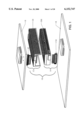
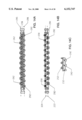
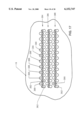
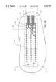
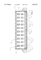
- FIG. 1 is an exploded sketch of a pair of overlying printed circuit boards electrically interconnected by a connector assembly according to the invention
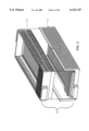
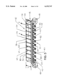
- FIG. 2 is a perspective, exploded drawing of one of a pair connectors of the connector assembly of FIG. 1;
- FIG. 3 is a perspective drawing of a housing of the connector of FIG. 2;
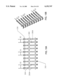
- FIG. 4 is a top view of a module used in the connector of FIG. 2;
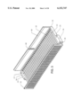
- FIG. 5 is a perspective view of the module of FIG. 4;
- FIG. 5A is a diagrammatic sketch showing the arrangement of proximal ends of electrical conductors of the module of FIG. 4;
- FIG. 5B is a diagrammatic sketch showing the arrangement of mounting pads of the module of FIG. 4;
- FIG. 6 is a different perspective view of the module of FIG. 4 with a shielding member thereof removed;
- FIG. 7 is a perspective view of a lead frame having a plurality of electrical signal conductors used in the module of FIG. 4;
- FIG. 8 is a cross-sectional sketch of a portion of the module of FIG. 4;
- FIG. 9 is a different perspective view of the module of FIG. 4;
- FIG. 10 is an exploded, perspective view of a portion of the module of FIG. 4;
- FIG. 11 is a perspective view of the shielding member of the module of FIG. 4;
- FIGS. 12A and 12B are different perspective drawings of a housing of the other one of the connectors of the connector assembly of FIG. 1;
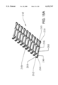
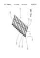
- FIG. 13 is an exploded, perspective view of a module used in the connector of FIG. 1;
- FIG. 14A is a diagrammatic sketch showing the arrangement of mounting pads of the module of FIG. 13;
- FIG. 14B is a diagrammatic sketch showing the arrangement of proximal ends of conductors of the module of FIG. 4;
- FIG. 14C is a cross-sectional sketch of a portion of the module of FIG. 4;
- FIGS. 15A and 15B are different perspective views of a lead frame of signal electrical conductors used in the module of FIG. 13;
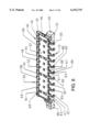
- FIG. 16 is a cross-sectional drawing of the connector assembly of FIG. 1;
- FIG. 17 is a top view of a portion of a printed circuit board having thereof a pad layout arranged for connection with one of the connectors of connector assembly of FIG. 1;
- FIG. 18 is a diagrammatical sketch showing the arrangement of signal conductors used in the printed circuit board of FIG. 17.
- FIGS. 19A and 19B are alternative embodiments of the signal lead frame shown in FIGS. 7 and 15A.
- the assembly 10 includes a pair of molded electrical connectors 12, 14.
- One of the electrical connectors, here connector 12 is adapted for mounting to a first printed circuit board 16 and the other electrical connector 14 is adapted for mounting to a second printed circuit board 18 positioned parallel to, here below, the first printed circuit board 16.
- connector 12 includes a dielectric, here plastic, housing 20, here a shroud, having a plurality of parallel slots 22 formed in an upper surface 24 thereof.
- the slots 22 extend between opposing sides 26, 28 of the housing 20.
- the housing 20 has a pair of opposing sidearms 30, 32 extending from the opposing sides 26, 28 in planes perpendicular to the slots 22.
- Housing 20 has disposed in an undersurface thereof a plurality of grooves 39. Each one of the grooves 39 is aligned with a corresponding one of the slots 22 providing for each one of the slots 22 an opposing, aligned pair of the grooves 39.
- the housing 20 has a pair of diagonally opposing mounting flanges 36, 38, each having a pair of holes therein for screws or pins, not shown, which may be used to fasten and align the housing to printed circuit board 16 (FIG. 1).
- the sidewall 30 has a slot 40 for enabling the housing 20 to key with a post, to be described, in the housing of connector 14.
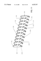
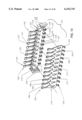
- the connector 12 includes a plurality of wafer-like modules 42 (sometimes referred to herein as merely wafers). Each one of the modules 42 is configured to be received in a corresponding one of the slots 22 (FIG. 3).
- each one of the modules 42 is identical in construction, an exemplary one thereof being shown in FIG. 4.
- Each one of such modules 42 includes a dielectric support 44, shown more clearly in FIGS. 5 and 6.
- the dielectric support 44 has a forward portion 46 and a pair of rearward, shoulder end portions 48.
- the forward portion 46 is adapted in to inserted into a corresponding one of the slots 22.
- the shoulder end portions 48 are configured to slide within a corresponding opposing pair of the grooves 39 (FIG. 3).
- the forward portion 46 of the dielectric support 44 has substantially planar opposing surface portions 50, 52, as shown in FIGS. 5 and 6, respectively.
- the surface portion 50 terminates along a beveled portion 54 disposed along a forward edge 56 of the dielectric support 44.
- the surface portion 52 (FIG. 6) terminates along beveled portions 58 interleaved with recesses 60 along the forward edge 56 of the dielectric support 44 to provide the support 44 with a spaced V-shaped forward edge 56.
- the module 42 includes a plurality of signal electrical conductors 62 disposed in a linear array. More particularly, the signal conductors 62 are provided in a copper lead frame 64 (FIG. 7). The lead frame 64 is insert molded into the dielectric support 44, as shown in FIG. 5. When assembled, portions 66 of the lead frame 64, which are connected between the adjacent conductors 62, are cut away along edges 67 (FIGS. 5 and 6) to provide electrically isolated conductors 62, as shown in FIG. 5. Each one of such signal electrical conductors 62 has: a forward, beveled proximal end 68 (FIGS.
- the signal electrical conductors 62 are electrically insulated one from another by interposed portions of the surface portion 50.
- central, elongated, upper portions 74 of the intermediate portion 70 are raised, as a rib-shaped structure, above the surface 50 of the dielectric support 44, as shown more clearly in FIG. 8. This raised structure can be formed by coining the edges of the signal electrical conductors 62 before they are molded into dielectric support 44.
- the rearward, distal end 72 includes a signal mounting pad 80 and a curved, here an arch-shaped, interconnect 82 disposed between an edge 83 of the signal mounting pad 80 and the intermediate portion 70.
- the interconnect 82 is resilient and suspends the signal mounting pad 80 at the edge 83 thereof beyond a rearward edge 85 (FIGS. 5 and 6) of the surface portion 50 in a region between the pair of rearward shoulder end portions 48 and in a nominal orientation substantially perpendicular to the surface portion 50.
- An opposite edge 87 of the signal mounting pad 80 being freely suspended outwardly from the surface portion 50.
- the mounting pads 80 are adapted for soldering to pads, not shown, on the printed circuit board 16 (FIG. 1).
- the mounting pads may be considered as contact tails.
- the pads 80 are configured to accept "solder spheres" 81 (FIG. 4) as on Ball Grid Array (BGA) packages. If desired, the spheres 81 can be placed on the pad 80, and then fused to the pad using a surface mount solder reflow process. The resulting structure is shown in FIG. 4.
- Mounting pads 80 can be shaped to facilitate attachment of a solder ball.
- FIG. 7 shows pad 80 stamped with a dimple 86 in it. Dimple 86 leaves a bump on the upper surface of the pad but creates a concave lower surface. The concave surface forces the solder ball into the center of pad 80 during reflow. Positional accuracy of the solder ball is enhanced before the connector is attached to the printed circuit board. A similar result can be obtained by forming a hole in the pad 80.
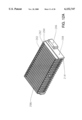
- the shield member 84 Disposed on the surface portion 52 (FIG. 6) of the dielectric support 44 is an electrical shielding member 84 as shown in FIG. 11.
- the shield member 84 is copper and stamped as shown in FIG. 11.
- the shielding member 84 includes a central region 88.
- the central region 88 has holes 89 stamped therein and such holes 89 are press-fit onto posts 91 molded, and projecting outwardly from, the surface portion 52, as shown in FIG. 6.
- the shielding member 84 has a forward plurality of openings 90 through which portion 58 (FIG. 6) of dielectric support 44 may project.
- Beveled portion 58 is insulative material backing the signal electrical conductors 68 thereby ensuring shield member 84 is not shorted to signal electrical conductors 68.
- Shielding member 84 has a beveled distal end 96 disposed in the recesses 60 (FIG. 6) along the forward edge 56 of the surface portion 52.
- the shielding member 84 also includes a rearward plurality of electrical reference potential conductors 98 (FIG. 11) having: proximal ends 100 terminating along a rearward edge 102 of central region 88; reference potential mounting pads 104; and reference potential arch-shaped interconnects 105 disposed between an edge 106 of the reference potential mounting pads 104 and the rearward edge 102 of the central region 88.
- a rearward plurality of electrical reference potential conductors 98 (FIG. 11) having: proximal ends 100 terminating along a rearward edge 102 of central region 88; reference potential mounting pads 104; and reference potential arch-shaped interconnects 105 disposed between an edge 106 of the reference potential mounting pads 104 and the rearward edge 102 of the central region 88.
- the reference potential arch-shaped interconnects 105 are resilient and suspend the reference potential mounting pads 104 at the edges 106 thereof beyond a rearward edge of the surface portion 52 in a region between the pair of shoulder end portions 48 and in a nominal orientation substantially perpendicular to the surface portion 52 with an opposite edge 110 of the reference potential mounting pad 104 being freely-suspended outward from the surface portion 52.
- the reference potential mounting pads 104 are freely suspended outward from the second surface portion 52 in a direction opposite to a direction of the suspended signal mounting pad 80 as shown in FIGS. 10 and 16.
- the mounting pads 104 like pads 80, are adapted for soldering to surface mounting pads 300, 302 (FIGS.
- the pads 104 are configured to accept "solder spheres" 107 (FIGS. 4, 9, and 10) as on Ball Grid Array (BGA) packages. If desired, the spheres can be placed on the pad 104, and then fused to the pad using a surface mount solder reflow process. The resulting structure is shown in FIG. 4 and 10.
- pads 104 do not extend below the lower edge of shoulders 48. Thus, when a wafer is mounted on a board, pads 204 (FIG. 12A) will be held above the surface of the board. The area below pad 104 will be filled with solder-forming a solder joint. Thus, mating forces are shared by the housing and the solder joints.
- the plurality of signal mounting pads 80 are disposed along a line 112 parallel to the rearward edge 85 of the dielectric support 44.
- the plurality of reference potential mounting pads 104 are disposed along a line 114 parallel to the rearward edge 85, the lines 112, 114 being disposed on opposite sides of the dielectric support 44. Further, the reference potential mounting pads 104 are staggered with the signal mounting pads 80 along the rearward edge 85 of the dielectric support 44.
- the conductive region 88 (FIG. 4), the elongated intermediate portions 70 of signal conductors 62 and the dielectric member 44 disposed therebetween are configured as microstrip transmission lines having a predetermined input impedance matched to the impedance of the printed circuit board 16, here an input impedance of 50 ohms.
- the length, L, (FIG. 5) of the transmission lines is easily extendable when longer modules are desired as for applications requiring greater height separation between the printed circuit boards 16, 18, FIG. 1. That is, the separation between boards 16, 18 is, in some applications, a function of the heat flow requirements between the boards 16, 18.
- the length is between 10 and 30 mm.
- the arch-shaped interconnects 82, 105 are configured to provide an inductor.
- the pads 80, 104 are here circular, or semi-circular shaped. These pads are attached to signal launches on a printed circuit board. The resulting interconnection will have a capacitive reactance. To counter-balance this capacitance the shape of the interconnects 82, 105 is selected to configure the interconnects 82, 105 as an inductor.
- the inductance of the interconnect 82, 105 and the capacitor of the pad 80, 104 are serially connected and configured to provide a series resonant circuit with the result that a signal on one printed circuit board propagates through the series resonant circuit to the strip transmission line described above.
- the other connector 14 is configured in a like manner so that the signal passes through an impedance matched microstrip transmission line therein and then through a similar series resonant circuit thereof.
- the connector 14 includes a dielectric, here plastic, housing 200.
- the housing 200 has a plurality of parallel slots 202 formed in an upper surface 204 thereof.
- the slots 202 extend longitudinally between opposing sides 206, 208 of the housing 200.
- the housing 200 has a pair of opposing sidearms 210, 212 extending from the opposing sides 206, 208 in planes perpendicular to the slots 202.
- Each one of the sidearms 210, 212 has disposed in surface portions thereof a plurality of grooves 214.
- Each one of the grooves 214 in each one of the sidearms 210, 212 is aligned with a corresponding one of the slots 202 providing for each one of the slots 202 an opposing, aligned pair of the grooves 214.
- the housing 202 has a pair of diagonally opposing mounting flanges 216, 218, each having a pair of holes therein for screws, or pins, not shown, which may be used to fasten or align the housing 200 to printed circuit board 18, FIG. 1.
- the sidewall 210 has a post 211 for enabling the housing 200 to key with the slot 40 (FIG. 3) in the sidearm 30 of housing 20.
- the connector 14 includes a plurality of wafer-like modules 230 (sometimes referred to herein as merely wafers). Each one of the modules 230 is identical in construction and is configured to be received in a corresponding one of the slots 202. An exemplary one of the modules 230 is shown in FIG. 13.
- Each one of the modules 230 includes a dielectric support 232 having a forward portion 234 and a pair of rearward, shoulder end portions 236. The end portions 236 are configured to slide within a corresponding opposing pair of the grooves 214 (FIGS. 12A and 12B).
- the forward portion 234 has substantially planar first and second opposing surfaces 240, shown in FIG. 13.
- the module 230 includes a plurality of signal electrical conductors 242 disposed in a linear array. More particularly, the signal conductors 242 are provided in a copper lead frame 246 (FIGS. 15A, 15B).
- the lead frame 246 is insert molded into the dielectric support 232 to form the structure shown in the right section of FIG. 13. When assembled, portions 249 of the lead frame 246 are cut away along edges 247 to provide electrically isolated conductors 242.
- Each one of the signal electrical conductors 242 has a forward, proximal end 248 made up of: a first concave-shaped electrical contact 250; and, a resilient, cantilever beam, interconnect 252 (FIG. 14C) suspending the contact 250 beyond a forward edge of the dielectric support 232.
- the contact 250 is adapted to have a forward portion 251 thereof engage the forward bevelled proximal end 68 (FIGS. 5 and 7) of a corresponding one of the plurality of signal electrical conductors 62 and bottom portions 253 thereof adapted to slide onto and electrically contact the central, elongated, upper rib portion 74 of the intermediate portion 70 of such corresponding one of the electrical signal conductors 62. That is, the raised, (i.e., upper), rib portion 74 has sufficient length to provide a full wipe along the bottom portion 253 of contact 250.
- Each one of the signal electrical conductors 242 includes an intermediate portion 260 embedded in the dielectric support 232. Each one of such signal electrical conductors 242 is electrically insulated one from another by interposed portions of the dielectric support 232. A forward portion of the intermediate portion 260 is connected to the forward proximal end 248 of a corresponding one of the signal conductors 242. A rearward, distal end of each one of the signal electrical conductors 242 includes a signal mounting pad 262 and an arch-shaped interconnect 264 disposed between a rearward portion of the intermediate portion 260 and an edge 266 of the signal mounting pad 262.
- the interconnect 264 is resilient and suspends the signal mounting pad 262 at the edge 266 thereof beyond the surface portion of the dielectric support 232 in a region between the pair of rearward shoulder end portions 236 and in a nominal orientation substantially perpendicular to the dielectric support 232 and with an opposite edge 268 of the signal pad 262 freely suspended outwardly from the dielectric support 232.
- the mounting pads 262 are configured like the pads 80 and 104 are therefore adapted for soldering to surface mounting pads 300, 302 (FIGS. 17, 18) on the printed circuit board 18 (FIG. 1). Further, the pads are configured to accept "solder spheres", not shown, as on Ball Grid Array (BGA) packages. If desired, the spheres can be placed on the pad, and then fused to the pad using a surface mount solder reflow process. Further, pads 262 and 292 are suspended in opposite directions as shown in FIG. 16.
- the module 230 includes an electrical shielding member 270 (FIG. 13).
- the electrical shielding member 270 includes a conductive, ground plane plate 272 disposed on the surface 240 of the dielectric support 232.
- the plate 272 has holes 273 stamped therein and such holes 273 are press-fit onto posts 275 molded, and projecting outwardly from, the surface 240, as shown in FIG. 13.
- the shielding member 270 includes a forward plurality of electrical reference potential conductors 282 having rearward proximal ends terminating along a forward edge of the plate 272.
- Each one of the forward plurality of reference potential conductors 282 includes a concave-shaped electrical contact 284 and a resilient, cantilever beam, interconnect 286 suspending the contact 284 beyond a forward edge of the dielectric support 232.
- contact 284 is adapted to make contact with beveled distal ends 96 of a corresponding one of the shielding members 84. the bottom portions 286 of the contacts 284 thereof slide onto and along the surface the conductive region 88 (FIGS. 9, 11, and 16).
- concave-shaped electrical contacts 250 are wider than signal electrical conductors 62. Thus, good electrical contact is made even if there is some misalignment between modules 42 and 230.
- the concave electrical contacts 250, 282 are staggered along the forward edge of the dielectric support 232, as shown in FIG. 14B, and have a gap 291 therebetween to receive the forward, edge of the dielectric support 44 of module 42, as shown in FIG. 16.
- contacts 250 are along line 320 and contacts 282 are along a parallel line 322, such lines 320, 322 being on opposite sides of dielectric support 232.
- the shielding member 270 also includes a rearward plurality of electrical reference potential conductors 290.
- the electrical reference potential electrical conductors 290 have proximal ends terminating along a rearward edge of the plate, reference potential mounting pads 292, and reference potential arch-shaped interconnects 294 disposed between an edge of the reference potential mounting pads and the rearward edge of the plate 272.
- the reference potential arch-shaped interconnects 294 are resilient and suspending the reference potential mounting pads 292 at the edges thereof beyond said a rearward edge of the dielectric support 232 in a region between the pair of shoulder end portions 236 and in a nominal orientation substantially perpendicular to the dielectric support 232 with an opposite edge of the reference potential mounting pad being freely suspended outwardly from the second surface of the dielectric support 240 as with pads 80, 104 and 262.
- the plurality of reference potential mounting pads 292 are identical in construction as pads 80, 104 and 262.
- the signal mounting pads 262 are disposed along a line 295 parallel to the rearward edge of the dielectric support 236.
- the plurality of reference potential mounting pads 292 are disposed along a line 296 parallel to the rearward edge of the dielectric support 236.
- the lines 295, 296 are disposed on opposite sides of the dielectric support 236, as shown in FIG. 14A.
- the reference potential mounting pads 292 are staggered with the signal mounting pads 262.
- center portions of arch-shaped interconnects 82 and the center portions of arch-shaped interconnects 105 overlaying one another in region 297 (FIG. 16) to provide a degree of shielding of adjacent interconnects 82 (which are coupled to signal) in center portions of interconnects 105 (which are coupled to a reference potential, such as ground).
- each of the interconnects 82, 105, 264 and 294 provides an inductor. It is also noted that the interconnects 82, 105, 264 and 294 also provide compliance to minimize mechanical stress on solder joints to the surface mounting pads 300, 302 (FIGS. 17, 18) by lowering the effective moment of inertia in the contact area.
- the conductive plate 272 (FIG. 13), the portions of signal conductors 242 embedded in the dielectric support 232 disposed therebetween are configured as microstrip transmission lines having an input impedance, here 50 ohms.
- the signal electrical conductors 62 and shielding member 84 are provided to mate with the signal electrical conductors 242 and contacts 284 of the modules 230 (FIG. 1) in housing 14, respectively, as shown in FIG. 16.
- FIG. 17 a layout of signal contact surface mounting pads 300 and ground contact surface mounting pads 302 for an exemplary one of the printed circuit boards 16, 18, here board 16, is shown.
- three rows 304, 306, 308, of contact surface mounting pads 300, 302 are shown.
- Between each pair of adjacent rows 304, 306, or 306, 308 are printed circuit board routing channels 311 (FIG. 18).
- FIG. 18 There are four signal lines 310 in one layer of a printed circuit board which may be routed to the signal contact surface mounting pads 300.
- both the signal contact pads and the ground contact pads are disposed along rows, with the signal contact pads being interleaved with the ground contact pads, as indicated.
- the pads 80, 104, 262, and 292 are preferably of semi-circular shape to facilitate the attachment of solder spheres and sized accordingly such that the sphere forms a cylinder or bulging sphere when reflow solder to the printed circuit board bridging the space between the pad and the surface mount pad on the printed circuit board.
- the cylinder may take a canted shape to allow the pad/surface mount pad misalignment.
- the conductors may optionally be coined on the underside to form a completely circular pad for attachment to the solder sphere reducing any tendency for the solder to wick up the conductor due to capillary action of solder wetting.
- the shoulder ends of the modules are alignment indicia and have ears for retaining the modules in the housing.
- the housing, or shroud transmits mating forces through the connectors 12 and 14 to boards 16 and 18, respectively. Thus, mating force shared by the housing or shroud and the solder joints.
- the modules are retained in the housings only at their ends providing a degree of compliance across the span between sidewalls and the housing. Whereas each module is individually retained, a degree of compliance or independence is also achieved from module to module.
- modules are retained in the direction across the shorter axis of the housing, parallel to the longitudinal axis of the housing to minimize any tendency to curt, or warp the housing as would be the case if the wafer were retained in the housing in the lengthwise, or elongated direction of the housing.
- wafers 42 and 230 are held in support members with tabs inserted into slots thereby forming an interference fit.
- Other attachment methods could be used.
- a snap fit connection might be used or metal barbs might be employed to provide a more secure connection if needed.
- the contact elements have contact tails that are adapted for a surface mount connection.
- the connector might be made with contact tails suitable for press-fit or through-hole connection.
- the disclosed embodiment shows a mezzanine type connector in which the signal contacts extend straight through wafers 42 and 230.
- Shield members 270 would likewise be modified to have contacts 282 on an edge that is perpendicular to the edge carrying rearward electrical connectors 290.
- all wafers in each connector portion are shown to be the same. However, such is not required. For example, some wafers might be adapted for carrying power. For a power wafer the conductors might be made wider to have a higher current carrying capacity or some of the conductors could be made of different lengths to provide a mate-first-break-last connection. Still further, differential wafers might be formed by jogging pairs of signal contacts closer together.
- wafers are held together in a housing or shroud.
- a connector could be assembled without either or both pieces.
- wafer 42 might be soldered directly to the printed circuit board 16 without the use of a shroud.
- all of the signal contacts in a wafer are evenly spaced. It might be advantageous to tailor the spacing between signal contacts to provide a desired level of performance.
- cross-talk associated with signal contacts at the end of a column is sometimes greater than the cross-talk associated with contacts at the center of a column.
- the performance of the connector is more balanced-meaning that all contacts have similar performance.
- FIG. 19A illustrates this construction. Comparing FIG. 19A to FIG. 15A, the intermediate portion 260A of the signal contacts at the end of the column are spaced from the intermediate portion 260 at the end of the next nearest signal contact by a distance D 2 . In contrast, the intermediate portions 260 in the center of the connector have a spacing of D 1 . Here, D 2 is larger than D 1 .
- FIG. 19A shows the spacing between pads 262 and contacts 250 is uniform. This arrangement is provided by jogs in the intermediate portions 260A.
- FIG. 19B shows a similar jogged arrangement for the signal contacts in wafer 42. Comparing FIG. 7 to FIG. 19B, it can be seen that FIG. 19B illustrates an embodiment in which the intermediate portions of the end signal contacts are jogged away from the intermediate portion of the nearest signal contact.
- a connector should be rated based on performance of the signal contact with the lowest performance tailoring the performance of one or two low performing signal contacts can increase the rated performance of the entire connector.
- the spacing between ground and signal contacts was selected to exactly match the impedance of signal traces in the printed circuit board. This spacing might be reduced to reduce cross-talk between adjacent signal conductors. Alternatively, the spacing might be adjusted to provide other impedances, which could be desired in other applications. The spacing, as well as the dimensions in the connector, will likely be set based on results of computer simulation and testing to provide performance levels suited for a given application.
- wafers are made with signal contacts on one side and ground contacts on the other. It might be desirable to have signal contacts on both sides of a wafer. Such a construction might be very useful for carrying differential signals.
- the end ones of the pads 104 and the interconnects 105 connected to such end pads 104 of shielding member 84 may be removed.
- the end ones of the pads 292 and the interconnects 294 connected to such end pads 292 of shielding member 270 may be removed.
Abstract
Description
Claims (9)
Priority Applications (3)
| Application Number | Priority Date | Filing Date | Title |
|---|---|---|---|
| US09/198,421 US6152747A (en) | 1998-11-24 | 1998-11-24 | Electrical connector |
| AU17419/00A AU1741900A (en) | 1998-11-24 | 1999-11-22 | Electrical connector |
| PCT/US1999/027650 WO2000031829A2 (en) | 1998-11-24 | 1999-11-22 | Electrical connector |
Applications Claiming Priority (1)
| Application Number | Priority Date | Filing Date | Title |
|---|---|---|---|
| US09/198,421 US6152747A (en) | 1998-11-24 | 1998-11-24 | Electrical connector |
Publications (1)
| Publication Number | Publication Date |
|---|---|
| US6152747A true US6152747A (en) | 2000-11-28 |
Family
ID=22733316
Family Applications (1)
| Application Number | Title | Priority Date | Filing Date |
|---|---|---|---|
| US09/198,421 Expired - Lifetime US6152747A (en) | 1998-11-24 | 1998-11-24 | Electrical connector |
Country Status (3)
| Country | Link |
|---|---|
| US (1) | US6152747A (en) |
| AU (1) | AU1741900A (en) |
| WO (1) | WO2000031829A2 (en) |
Cited By (99)
| Publication number | Priority date | Publication date | Assignee | Title |
|---|---|---|---|---|
| US6406316B1 (en) | 1998-01-31 | 2002-06-18 | Fci Americas Technology, Inc. | Electrical connector with multiple housings |
| US6623310B1 (en) * | 2002-05-21 | 2003-09-23 | Hon Hai Precision Ind. Co., Ltd. | High density electrical connector assembly with reduced insertion force |
| US20030179049A1 (en) * | 2002-02-05 | 2003-09-25 | Force10 Networks, Inc. | Passive transmission line equalization using circuit-board thru-holes |
| US6638110B1 (en) | 2002-05-22 | 2003-10-28 | Hon Hai Precision Ind. Co., Ltd. | High density electrical connector |
| US6638079B1 (en) * | 2002-05-21 | 2003-10-28 | Hon Hai Precision Ind. Co., Ltd. | Customizable electrical connector |
| US6641410B2 (en) | 2001-06-07 | 2003-11-04 | Teradyne, Inc. | Electrical solder ball contact |
| US6645010B1 (en) * | 2002-06-07 | 2003-11-11 | Hon Hai Precision Ind. Co., Ltd. | High density electrical connector with improved grounding bus |
| US6645009B1 (en) * | 2002-06-04 | 2003-11-11 | Hon Hai Precision Ind. Co., Ltd. | High density electrical connector with lead-in device |
| US6648689B1 (en) | 2002-06-07 | 2003-11-18 | Hon Hai Precision Ind. Co., Ltd. | High density electrical connector having enhanced crosstalk reduction capability |
| US6663429B1 (en) | 2002-08-29 | 2003-12-16 | Hon Hai Precision Ind. Co., Ltd. | Method for manufacturing high density electrical connector assembly |
| US6682369B1 (en) | 2002-09-18 | 2004-01-27 | Hon Hai Precision Ind. Co., Ltd. | Electrical connector having retention system for precisely mounting plural boards therein |
| US20040018757A1 (en) * | 2002-05-06 | 2004-01-29 | Lang Harold Keith | Board-to-board connector with compliant mounting pins |
| US6780057B2 (en) * | 2001-12-21 | 2004-08-24 | Intel Corporation | Coaxial dual pin sockets for high speed I/O applications |
| US20040248432A1 (en) * | 2003-06-04 | 2004-12-09 | Barr Andrew Harvey | Connector having a bypass capacitor and method for reducing the impedance and length of a return-signal path |
| WO2005004288A2 (en) * | 2003-06-26 | 2005-01-13 | Amphenol Corporation | High speed, high density electrical connector |
| US20050048838A1 (en) * | 2003-08-29 | 2005-03-03 | Korsunsky Iosif R. | Electrical connector having circuit board modules positioned between metal stiffener and a housing |
| US6905367B2 (en) | 2002-07-16 | 2005-06-14 | Silicon Bandwidth, Inc. | Modular coaxial electrical interconnect system having a modular frame and electrically shielded signal paths and a method of making the same |
| US20060160380A1 (en) * | 2005-01-20 | 2006-07-20 | Hon Hai Precision Ind. Co., Ltd. | Mating extender for electrically connecting with two electrical connectors |
| US20070207635A1 (en) * | 2005-11-29 | 2007-09-06 | Gailus Mark W | Electronic component with high density, low cost attachment |
| US20070287336A1 (en) * | 2006-06-09 | 2007-12-13 | Buck Jonathan E | Electrical connectors with alignment guides |
| US20080293264A1 (en) * | 2007-05-22 | 2008-11-27 | Tyco Electronics Corporation | Single use security module mezzanine connector |
| US20080293272A1 (en) * | 2007-05-22 | 2008-11-27 | Tyco Electronics Corporation | Two piece single use security module mezzanine connector |
| US20090130912A1 (en) * | 2007-11-15 | 2009-05-21 | Fci Americas Technology, Inc. | Electrical connector mating guide |
| US20100055988A1 (en) * | 2007-08-30 | 2010-03-04 | Shuey Joseph B | Mezzanine-type electrical connectors |
| US20100167569A1 (en) * | 2008-12-31 | 2010-07-01 | Stoner Stuart C | Gender-Neutral Electrical Connector |
| US7762843B2 (en) | 2006-12-19 | 2010-07-27 | Fci Americas Technology, Inc. | Shieldless, high-speed, low-cross-talk electrical connector |
| US7837505B2 (en) | 2006-08-21 | 2010-11-23 | Fci Americas Technology Llc | Electrical connector system with jogged contact tails |
| US8137119B2 (en) | 2007-07-13 | 2012-03-20 | Fci Americas Technology Llc | Electrical connector system having a continuous ground at the mating interface thereof |
| WO2012106554A2 (en) * | 2011-02-02 | 2012-08-09 | Amphenol Corporation | Mezzanine connector |
| US8267721B2 (en) | 2009-10-28 | 2012-09-18 | Fci Americas Technology Llc | Electrical connector having ground plates and ground coupling bar |
| US8277241B2 (en) | 2008-09-25 | 2012-10-02 | Fci Americas Technology Llc | Hermaphroditic electrical connector |
| US8540525B2 (en) | 2008-12-12 | 2013-09-24 | Molex Incorporated | Resonance modifying connector |
| US8545240B2 (en) | 2008-11-14 | 2013-10-01 | Molex Incorporated | Connector with terminals forming differential pairs |
| US8616919B2 (en) | 2009-11-13 | 2013-12-31 | Fci Americas Technology Llc | Attachment system for electrical connector |
| US8764464B2 (en) | 2008-02-29 | 2014-07-01 | Fci Americas Technology Llc | Cross talk reduction for high speed electrical connectors |
| US8771016B2 (en) | 2010-02-24 | 2014-07-08 | Amphenol Corporation | High bandwidth connector |
| US8864521B2 (en) | 2005-06-30 | 2014-10-21 | Amphenol Corporation | High frequency electrical connector |
| USD718253S1 (en) | 2012-04-13 | 2014-11-25 | Fci Americas Technology Llc | Electrical cable connector |
| US8905651B2 (en) | 2012-01-31 | 2014-12-09 | Fci | Dismountable optical coupling device |
| USD720698S1 (en) | 2013-03-15 | 2015-01-06 | Fci Americas Technology Llc | Electrical cable connector |
| US8926377B2 (en) | 2009-11-13 | 2015-01-06 | Amphenol Corporation | High performance, small form factor connector with common mode impedance control |
| US8944831B2 (en) | 2012-04-13 | 2015-02-03 | Fci Americas Technology Llc | Electrical connector having ribbed ground plate with engagement members |
| US20150064971A1 (en) * | 2013-08-30 | 2015-03-05 | Fujitsu Limited | Connector and manufacturing method thereof |
| US9004942B2 (en) | 2011-10-17 | 2015-04-14 | Amphenol Corporation | Electrical connector with hybrid shield |
| USD727268S1 (en) | 2012-04-13 | 2015-04-21 | Fci Americas Technology Llc | Vertical electrical connector |
| USD727852S1 (en) | 2012-04-13 | 2015-04-28 | Fci Americas Technology Llc | Ground shield for a right angle electrical connector |
| US9022806B2 (en) | 2012-06-29 | 2015-05-05 | Amphenol Corporation | Printed circuit board for RF connector mounting |
| US9048583B2 (en) | 2009-03-19 | 2015-06-02 | Fci Americas Technology Llc | Electrical connector having ribbed ground plate |
| USD733662S1 (en) | 2013-01-25 | 2015-07-07 | Fci Americas Technology Llc | Connector housing for electrical connector |
| USD746236S1 (en) | 2012-07-11 | 2015-12-29 | Fci Americas Technology Llc | Electrical connector housing |
| US9257778B2 (en) | 2012-04-13 | 2016-02-09 | Fci Americas Technology | High speed electrical connector |
| US9277649B2 (en) | 2009-02-26 | 2016-03-01 | Fci Americas Technology Llc | Cross talk reduction for high-speed electrical connectors |
| US9450344B2 (en) | 2014-01-22 | 2016-09-20 | Amphenol Corporation | High speed, high density electrical connector with shielded signal paths |
| US9484674B2 (en) | 2013-03-14 | 2016-11-01 | Amphenol Corporation | Differential electrical connector with improved skew control |
| US9520689B2 (en) | 2013-03-13 | 2016-12-13 | Amphenol Corporation | Housing for a high speed electrical connector |
| US9543703B2 (en) | 2012-07-11 | 2017-01-10 | Fci Americas Technology Llc | Electrical connector with reduced stack height |
| US9831588B2 (en) | 2012-08-22 | 2017-11-28 | Amphenol Corporation | High-frequency electrical connector |
| US10122129B2 (en) | 2010-05-07 | 2018-11-06 | Amphenol Corporation | High performance cable connector |
| US10205286B2 (en) | 2016-10-19 | 2019-02-12 | Amphenol Corporation | Compliant shield for very high speed, high density electrical interconnection |
| US10243304B2 (en) | 2016-08-23 | 2019-03-26 | Amphenol Corporation | Connector configurable for high performance |
| US10541482B2 (en) | 2015-07-07 | 2020-01-21 | Amphenol Fci Asia Pte. Ltd. | Electrical connector with cavity between terminals |
| US10601181B2 (en) | 2017-12-01 | 2020-03-24 | Amphenol East Asia Ltd. | Compact electrical connector |
| US10651603B2 (en) | 2016-06-01 | 2020-05-12 | Amphenol Fci Connectors Singapore Pte. Ltd. | High speed electrical connector |
| US10777921B2 (en) | 2017-12-06 | 2020-09-15 | Amphenol East Asia Ltd. | High speed card edge connector |
| US10840649B2 (en) | 2014-11-12 | 2020-11-17 | Amphenol Corporation | Organizer for a very high speed, high density electrical interconnection system |
| US10879643B2 (en) | 2015-07-23 | 2020-12-29 | Amphenol Corporation | Extender module for modular connector |
| US10879650B2 (en) * | 2018-12-11 | 2020-12-29 | Lotes Co., Ltd | Electrical connector |
| US10931062B2 (en) | 2018-11-21 | 2021-02-23 | Amphenol Corporation | High-frequency electrical connector |
| US10944189B2 (en) | 2018-09-26 | 2021-03-09 | Amphenol East Asia Electronic Technology (Shenzhen) Co., Ltd. | High speed electrical connector and printed circuit board thereof |
| US10965064B2 (en) | 2019-04-22 | 2021-03-30 | Amphenol East Asia Ltd. | SMT receptacle connector with side latching |
| US11070006B2 (en) | 2017-08-03 | 2021-07-20 | Amphenol Corporation | Connector for low loss interconnection system |
| US11101611B2 (en) | 2019-01-25 | 2021-08-24 | Fci Usa Llc | I/O connector configured for cabled connection to the midboard |
| US11189971B2 (en) | 2019-02-14 | 2021-11-30 | Amphenol East Asia Ltd. | Robust, high-frequency electrical connector |
| US11189943B2 (en) | 2019-01-25 | 2021-11-30 | Fci Usa Llc | I/O connector configured for cable connection to a midboard |
| US11205877B2 (en) | 2018-04-02 | 2021-12-21 | Ardent Concepts, Inc. | Controlled-impedance compliant cable termination |
| US11217942B2 (en) | 2018-11-15 | 2022-01-04 | Amphenol East Asia Ltd. | Connector having metal shell with anti-displacement structure |
| US11381015B2 (en) | 2018-12-21 | 2022-07-05 | Amphenol East Asia Ltd. | Robust, miniaturized card edge connector |
| US11437762B2 (en) | 2019-02-22 | 2022-09-06 | Amphenol Corporation | High performance cable connector assembly |
| US11444398B2 (en) | 2018-03-22 | 2022-09-13 | Amphenol Corporation | High density electrical connector |
| US11469554B2 (en) | 2020-01-27 | 2022-10-11 | Fci Usa Llc | High speed, high density direct mate orthogonal connector |
| US11569613B2 (en) | 2021-04-19 | 2023-01-31 | Amphenol East Asia Ltd. | Electrical connector having symmetrical docking holes |
| US11588277B2 (en) | 2019-11-06 | 2023-02-21 | Amphenol East Asia Ltd. | High-frequency electrical connector with lossy member |
| US11637391B2 (en) | 2020-03-13 | 2023-04-25 | Amphenol Commercial Products (Chengdu) Co., Ltd. | Card edge connector with strength member, and circuit board assembly |
| US11652307B2 (en) | 2020-08-20 | 2023-05-16 | Amphenol East Asia Electronic Technology (Shenzhen) Co., Ltd. | High speed connector |
| US11670879B2 (en) | 2020-01-28 | 2023-06-06 | Fci Usa Llc | High frequency midboard connector |
| US11710917B2 (en) | 2017-10-30 | 2023-07-25 | Amphenol Fci Asia Pte. Ltd. | Low crosstalk card edge connector |
| US11728585B2 (en) | 2020-06-17 | 2023-08-15 | Amphenol East Asia Ltd. | Compact electrical connector with shell bounding spaces for receiving mating protrusions |
| US11735852B2 (en) | 2019-09-19 | 2023-08-22 | Amphenol Corporation | High speed electronic system with midboard cable connector |
| US11742601B2 (en) | 2019-05-20 | 2023-08-29 | Amphenol Corporation | High density, high speed electrical connector |
| USD1002553S1 (en) | 2021-11-03 | 2023-10-24 | Amphenol Corporation | Gasket for connector |
| US11799246B2 (en) | 2020-01-27 | 2023-10-24 | Fci Usa Llc | High speed connector |
| US11799230B2 (en) | 2019-11-06 | 2023-10-24 | Amphenol East Asia Ltd. | High-frequency electrical connector with in interlocking segments |
| US11817655B2 (en) | 2020-09-25 | 2023-11-14 | Amphenol Commercial Products (Chengdu) Co., Ltd. | Compact, high speed electrical connector |
| US11817639B2 (en) | 2020-08-31 | 2023-11-14 | Amphenol Commercial Products (Chengdu) Co., Ltd. | Miniaturized electrical connector for compact electronic system |
| US11831092B2 (en) | 2020-07-28 | 2023-11-28 | Amphenol East Asia Ltd. | Compact electrical connector |
| US11831106B2 (en) | 2016-05-31 | 2023-11-28 | Amphenol Corporation | High performance cable termination |
| US11870171B2 (en) | 2018-10-09 | 2024-01-09 | Amphenol Commercial Products (Chengdu) Co., Ltd. | High-density edge connector |
| US11942716B2 (en) | 2020-09-22 | 2024-03-26 | Amphenol Commercial Products (Chengdu) Co., Ltd. | High speed electrical connector |
| US11955742B2 (en) | 2015-07-07 | 2024-04-09 | Amphenol Fci Asia Pte. Ltd. | Electrical connector with cavity between terminals |
Citations (19)
| Publication number | Priority date | Publication date | Assignee | Title |
|---|---|---|---|---|
| US4984992A (en) * | 1989-11-01 | 1991-01-15 | Amp Incorporated | Cable connector with a low inductance path |
| US5035632A (en) * | 1989-10-10 | 1991-07-30 | Itt Corporation | Card connector with interceptor plate |
| US5224867A (en) * | 1990-10-08 | 1993-07-06 | Daiichi Denshi Kogyo Kabushiki Kaisha | Electrical connector for coaxial flat cable |
| US5299956A (en) * | 1992-03-23 | 1994-04-05 | Superior Modular Products, Inc. | Low cross talk electrical connector system |
| US5362257A (en) * | 1993-07-08 | 1994-11-08 | The Whitaker Corporation | Communications connector terminal arrays having noise cancelling capabilities |
| US5545051A (en) * | 1995-06-28 | 1996-08-13 | The Whitaker Corporation | Board to board matable assembly |
| WO1996038889A1 (en) * | 1995-05-31 | 1996-12-05 | Teradyne, Inc. | Surface mounted electrical connector |
| US5586914A (en) * | 1995-05-19 | 1996-12-24 | The Whitaker Corporation | Electrical connector and an associated method for compensating for crosstalk between a plurality of conductors |
| EP0766352A2 (en) * | 1995-09-29 | 1997-04-02 | KRONE Aktiengesellschaft | Terminal block with high transmission rate |
| US5626482A (en) * | 1994-12-15 | 1997-05-06 | Molex Incorporated | Low profile surface mountable electrical connector assembly |
| US5667393A (en) * | 1995-07-14 | 1997-09-16 | Grabbe; Dimitry | Printed circuit board electrical connector with sealed housing cavity |
| US5704794A (en) * | 1986-12-29 | 1998-01-06 | Labinal Components And Systems, Inc. | Electrical connectors |
| WO1998002942A2 (en) * | 1996-07-17 | 1998-01-22 | Minnesota Mining And Manufacturing Company | Electrical interconnection system and device |
| WO1998004020A1 (en) * | 1996-07-23 | 1998-01-29 | Superior Modular Products Incorporated | Reduced cross talk electrical connector |
| WO1998009354A1 (en) * | 1996-08-30 | 1998-03-05 | The Whitaker Corporation | Ground-power plane connector |
| US5813871A (en) * | 1996-07-31 | 1998-09-29 | The Whitaker Corporation | High frequency electrical connector |
| US5915975A (en) * | 1996-09-12 | 1999-06-29 | Molex Incorporated | Surface mount connector with integrated power leads |
| US5944540A (en) * | 1997-02-17 | 1999-08-31 | Kabushiki Kaisha Toshiba | Operation assuring structure of electronic circuit board in connector for said circuit board |
| US6036549A (en) * | 1996-04-22 | 2000-03-14 | Siemens Aktiengesellschaft | Plug-in connector with contact surface protection in the plug-in opening area |
-
1998
- 1998-11-24 US US09/198,421 patent/US6152747A/en not_active Expired - Lifetime
-
1999
- 1999-11-22 AU AU17419/00A patent/AU1741900A/en not_active Abandoned
- 1999-11-22 WO PCT/US1999/027650 patent/WO2000031829A2/en active Application Filing
Patent Citations (20)
| Publication number | Priority date | Publication date | Assignee | Title |
|---|---|---|---|---|
| US5704794A (en) * | 1986-12-29 | 1998-01-06 | Labinal Components And Systems, Inc. | Electrical connectors |
| US5035632A (en) * | 1989-10-10 | 1991-07-30 | Itt Corporation | Card connector with interceptor plate |
| US4984992A (en) * | 1989-11-01 | 1991-01-15 | Amp Incorporated | Cable connector with a low inductance path |
| US5224867A (en) * | 1990-10-08 | 1993-07-06 | Daiichi Denshi Kogyo Kabushiki Kaisha | Electrical connector for coaxial flat cable |
| US5299956A (en) * | 1992-03-23 | 1994-04-05 | Superior Modular Products, Inc. | Low cross talk electrical connector system |
| US5299956B1 (en) * | 1992-03-23 | 1995-10-24 | Superior Modular Prod Inc | Low cross talk electrical connector system |
| US5362257A (en) * | 1993-07-08 | 1994-11-08 | The Whitaker Corporation | Communications connector terminal arrays having noise cancelling capabilities |
| US5626482A (en) * | 1994-12-15 | 1997-05-06 | Molex Incorporated | Low profile surface mountable electrical connector assembly |
| US5586914A (en) * | 1995-05-19 | 1996-12-24 | The Whitaker Corporation | Electrical connector and an associated method for compensating for crosstalk between a plurality of conductors |
| WO1996038889A1 (en) * | 1995-05-31 | 1996-12-05 | Teradyne, Inc. | Surface mounted electrical connector |
| US5545051A (en) * | 1995-06-28 | 1996-08-13 | The Whitaker Corporation | Board to board matable assembly |
| US5667393A (en) * | 1995-07-14 | 1997-09-16 | Grabbe; Dimitry | Printed circuit board electrical connector with sealed housing cavity |
| EP0766352A2 (en) * | 1995-09-29 | 1997-04-02 | KRONE Aktiengesellschaft | Terminal block with high transmission rate |
| US6036549A (en) * | 1996-04-22 | 2000-03-14 | Siemens Aktiengesellschaft | Plug-in connector with contact surface protection in the plug-in opening area |
| WO1998002942A2 (en) * | 1996-07-17 | 1998-01-22 | Minnesota Mining And Manufacturing Company | Electrical interconnection system and device |
| WO1998004020A1 (en) * | 1996-07-23 | 1998-01-29 | Superior Modular Products Incorporated | Reduced cross talk electrical connector |
| US5813871A (en) * | 1996-07-31 | 1998-09-29 | The Whitaker Corporation | High frequency electrical connector |
| WO1998009354A1 (en) * | 1996-08-30 | 1998-03-05 | The Whitaker Corporation | Ground-power plane connector |
| US5915975A (en) * | 1996-09-12 | 1999-06-29 | Molex Incorporated | Surface mount connector with integrated power leads |
| US5944540A (en) * | 1997-02-17 | 1999-08-31 | Kabushiki Kaisha Toshiba | Operation assuring structure of electronic circuit board in connector for said circuit board |
Cited By (182)
| Publication number | Priority date | Publication date | Assignee | Title |
|---|---|---|---|---|
| US6406316B1 (en) | 1998-01-31 | 2002-06-18 | Fci Americas Technology, Inc. | Electrical connector with multiple housings |
| US6641410B2 (en) | 2001-06-07 | 2003-11-04 | Teradyne, Inc. | Electrical solder ball contact |
| US6780057B2 (en) * | 2001-12-21 | 2004-08-24 | Intel Corporation | Coaxial dual pin sockets for high speed I/O applications |
| US6812803B2 (en) * | 2002-02-05 | 2004-11-02 | Force10 Networks, Inc. | Passive transmission line equalization using circuit-board thru-holes |
| US20030179049A1 (en) * | 2002-02-05 | 2003-09-25 | Force10 Networks, Inc. | Passive transmission line equalization using circuit-board thru-holes |
| US6863543B2 (en) * | 2002-05-06 | 2005-03-08 | Molex Incorporated | Board-to-board connector with compliant mounting pins |
| US20040018757A1 (en) * | 2002-05-06 | 2004-01-29 | Lang Harold Keith | Board-to-board connector with compliant mounting pins |
| US6638079B1 (en) * | 2002-05-21 | 2003-10-28 | Hon Hai Precision Ind. Co., Ltd. | Customizable electrical connector |
| US6623310B1 (en) * | 2002-05-21 | 2003-09-23 | Hon Hai Precision Ind. Co., Ltd. | High density electrical connector assembly with reduced insertion force |
| US20030220019A1 (en) * | 2002-05-22 | 2003-11-27 | Billman Timothy B. | High density electrical connector assembly |
| US6663427B1 (en) * | 2002-05-22 | 2003-12-16 | Hon Hai Precision Ind. Co., Ltd. | High density electrical connector assembly |
| US6638110B1 (en) | 2002-05-22 | 2003-10-28 | Hon Hai Precision Ind. Co., Ltd. | High density electrical connector |
| US6645009B1 (en) * | 2002-06-04 | 2003-11-11 | Hon Hai Precision Ind. Co., Ltd. | High density electrical connector with lead-in device |
| US6648689B1 (en) | 2002-06-07 | 2003-11-18 | Hon Hai Precision Ind. Co., Ltd. | High density electrical connector having enhanced crosstalk reduction capability |
| US6645010B1 (en) * | 2002-06-07 | 2003-11-11 | Hon Hai Precision Ind. Co., Ltd. | High density electrical connector with improved grounding bus |
| US6905367B2 (en) | 2002-07-16 | 2005-06-14 | Silicon Bandwidth, Inc. | Modular coaxial electrical interconnect system having a modular frame and electrically shielded signal paths and a method of making the same |
| US6663429B1 (en) | 2002-08-29 | 2003-12-16 | Hon Hai Precision Ind. Co., Ltd. | Method for manufacturing high density electrical connector assembly |
| US6682369B1 (en) | 2002-09-18 | 2004-01-27 | Hon Hai Precision Ind. Co., Ltd. | Electrical connector having retention system for precisely mounting plural boards therein |
| US20040248432A1 (en) * | 2003-06-04 | 2004-12-09 | Barr Andrew Harvey | Connector having a bypass capacitor and method for reducing the impedance and length of a return-signal path |
| US7513779B2 (en) * | 2003-06-04 | 2009-04-07 | Hewlett-Packard Development Company, L.P. | Connector having a bypass capacitor and method for reducing the impedance and length of a return-signal path |
| WO2005004288A3 (en) * | 2003-06-26 | 2005-03-03 | Teradyne Inc | High speed, high density electrical connector |
| WO2005004288A2 (en) * | 2003-06-26 | 2005-01-13 | Amphenol Corporation | High speed, high density electrical connector |
| CN100405666C (en) * | 2003-06-26 | 2008-07-23 | 泰拉丁公司 | High speed, high density electrical connector and connector assembly |
| US20050048838A1 (en) * | 2003-08-29 | 2005-03-03 | Korsunsky Iosif R. | Electrical connector having circuit board modules positioned between metal stiffener and a housing |
| US6884117B2 (en) * | 2003-08-29 | 2005-04-26 | Hon Hai Precision Ind. Co., Ltd. | Electrical connector having circuit board modules positioned between metal stiffener and a housing |
| US7104808B2 (en) | 2005-01-20 | 2006-09-12 | Hon Hai Precision Ind. Co., Ltd. | Mating extender for electrically connecting with two electrical connectors |
| US20060160380A1 (en) * | 2005-01-20 | 2006-07-20 | Hon Hai Precision Ind. Co., Ltd. | Mating extender for electrically connecting with two electrical connectors |
| US8864521B2 (en) | 2005-06-30 | 2014-10-21 | Amphenol Corporation | High frequency electrical connector |
| US9219335B2 (en) | 2005-06-30 | 2015-12-22 | Amphenol Corporation | High frequency electrical connector |
| US9705255B2 (en) | 2005-06-30 | 2017-07-11 | Amphenol Corporation | High frequency electrical connector |
| US20070207635A1 (en) * | 2005-11-29 | 2007-09-06 | Gailus Mark W | Electronic component with high density, low cost attachment |
| US7484971B2 (en) | 2005-11-29 | 2009-02-03 | Amphenol Corporation | Electronic component with high density, low cost attachment |
| US20070287336A1 (en) * | 2006-06-09 | 2007-12-13 | Buck Jonathan E | Electrical connectors with alignment guides |
| US7553182B2 (en) | 2006-06-09 | 2009-06-30 | Fci Americas Technology, Inc. | Electrical connectors with alignment guides |
| US7837505B2 (en) | 2006-08-21 | 2010-11-23 | Fci Americas Technology Llc | Electrical connector system with jogged contact tails |
| US7762843B2 (en) | 2006-12-19 | 2010-07-27 | Fci Americas Technology, Inc. | Shieldless, high-speed, low-cross-talk electrical connector |
| US8382521B2 (en) | 2006-12-19 | 2013-02-26 | Fci Americas Technology Llc | Shieldless, high-speed, low-cross-talk electrical connector |
| US8678860B2 (en) | 2006-12-19 | 2014-03-25 | Fci Americas Technology Llc | Shieldless, high-speed, low-cross-talk electrical connector |
| US8096832B2 (en) | 2006-12-19 | 2012-01-17 | Fci Americas Technology Llc | Shieldless, high-speed, low-cross-talk electrical connector |
| US7597581B2 (en) | 2007-05-22 | 2009-10-06 | Tyco Electronics Corporation | Single use security module mezzanine connector |
| US7470129B2 (en) | 2007-05-22 | 2008-12-30 | Tyco Electronics Corporation | Two piece single use security module mezzanine connector |
| US20080293272A1 (en) * | 2007-05-22 | 2008-11-27 | Tyco Electronics Corporation | Two piece single use security module mezzanine connector |
| US20080293264A1 (en) * | 2007-05-22 | 2008-11-27 | Tyco Electronics Corporation | Single use security module mezzanine connector |
| US8137119B2 (en) | 2007-07-13 | 2012-03-20 | Fci Americas Technology Llc | Electrical connector system having a continuous ground at the mating interface thereof |
| US8147268B2 (en) | 2007-08-30 | 2012-04-03 | Fci Americas Technology Llc | Mezzanine-type electrical connectors |
| US20100055988A1 (en) * | 2007-08-30 | 2010-03-04 | Shuey Joseph B | Mezzanine-type electrical connectors |
| US8147254B2 (en) | 2007-11-15 | 2012-04-03 | Fci Americas Technology Llc | Electrical connector mating guide |
| US20090130912A1 (en) * | 2007-11-15 | 2009-05-21 | Fci Americas Technology, Inc. | Electrical connector mating guide |
| US8764464B2 (en) | 2008-02-29 | 2014-07-01 | Fci Americas Technology Llc | Cross talk reduction for high speed electrical connectors |
| US8277241B2 (en) | 2008-09-25 | 2012-10-02 | Fci Americas Technology Llc | Hermaphroditic electrical connector |
| US8545240B2 (en) | 2008-11-14 | 2013-10-01 | Molex Incorporated | Connector with terminals forming differential pairs |
| US8540525B2 (en) | 2008-12-12 | 2013-09-24 | Molex Incorporated | Resonance modifying connector |
| US8651881B2 (en) | 2008-12-12 | 2014-02-18 | Molex Incorporated | Resonance modifying connector |
| US8992237B2 (en) | 2008-12-12 | 2015-03-31 | Molex Incorporated | Resonance modifying connector |
| US20100167569A1 (en) * | 2008-12-31 | 2010-07-01 | Stoner Stuart C | Gender-Neutral Electrical Connector |
| US7976326B2 (en) | 2008-12-31 | 2011-07-12 | Fci Americas Technology Llc | Gender-neutral electrical connector |
| US9277649B2 (en) | 2009-02-26 | 2016-03-01 | Fci Americas Technology Llc | Cross talk reduction for high-speed electrical connectors |
| US9461410B2 (en) | 2009-03-19 | 2016-10-04 | Fci Americas Technology Llc | Electrical connector having ribbed ground plate |
| US10096921B2 (en) | 2009-03-19 | 2018-10-09 | Fci Usa Llc | Electrical connector having ribbed ground plate |
| US10720721B2 (en) | 2009-03-19 | 2020-07-21 | Fci Usa Llc | Electrical connector having ribbed ground plate |
| US9048583B2 (en) | 2009-03-19 | 2015-06-02 | Fci Americas Technology Llc | Electrical connector having ribbed ground plate |
| US8267721B2 (en) | 2009-10-28 | 2012-09-18 | Fci Americas Technology Llc | Electrical connector having ground plates and ground coupling bar |
| US8616919B2 (en) | 2009-11-13 | 2013-12-31 | Fci Americas Technology Llc | Attachment system for electrical connector |
| US8926377B2 (en) | 2009-11-13 | 2015-01-06 | Amphenol Corporation | High performance, small form factor connector with common mode impedance control |
| US9028281B2 (en) | 2009-11-13 | 2015-05-12 | Amphenol Corporation | High performance, small form factor connector |
| US8771016B2 (en) | 2010-02-24 | 2014-07-08 | Amphenol Corporation | High bandwidth connector |
| US10122129B2 (en) | 2010-05-07 | 2018-11-06 | Amphenol Corporation | High performance cable connector |
| US10381767B1 (en) | 2010-05-07 | 2019-08-13 | Amphenol Corporation | High performance cable connector |
| US11757224B2 (en) | 2010-05-07 | 2023-09-12 | Amphenol Corporation | High performance cable connector |
| WO2012106554A2 (en) * | 2011-02-02 | 2012-08-09 | Amphenol Corporation | Mezzanine connector |
| CN103477503B (en) * | 2011-02-02 | 2016-01-20 | 安费诺有限公司 | Mezzanine connector |
| CN103477503A (en) * | 2011-02-02 | 2013-12-25 | 安费诺有限公司 | Mezzanine connector |
| US8636543B2 (en) | 2011-02-02 | 2014-01-28 | Amphenol Corporation | Mezzanine connector |
| US8657627B2 (en) | 2011-02-02 | 2014-02-25 | Amphenol Corporation | Mezzanine connector |
| US8491313B2 (en) | 2011-02-02 | 2013-07-23 | Amphenol Corporation | Mezzanine connector |
| WO2012106554A3 (en) * | 2011-02-02 | 2012-11-01 | Amphenol Corporation | Mezzanine connector |
| US8801464B2 (en) | 2011-02-02 | 2014-08-12 | Amphenol Corporation | Mezzanine connector |
| US9660384B2 (en) | 2011-10-17 | 2017-05-23 | Amphenol Corporation | Electrical connector with hybrid shield |
| US9004942B2 (en) | 2011-10-17 | 2015-04-14 | Amphenol Corporation | Electrical connector with hybrid shield |
| US8905651B2 (en) | 2012-01-31 | 2014-12-09 | Fci | Dismountable optical coupling device |
| USD816044S1 (en) | 2012-04-13 | 2018-04-24 | Fci Americas Technology Llc | Electrical cable connector |
| USD790471S1 (en) | 2012-04-13 | 2017-06-27 | Fci Americas Technology Llc | Vertical electrical connector |
| USD748063S1 (en) | 2012-04-13 | 2016-01-26 | Fci Americas Technology Llc | Electrical ground shield |
| US9257778B2 (en) | 2012-04-13 | 2016-02-09 | Fci Americas Technology | High speed electrical connector |
| USD750030S1 (en) | 2012-04-13 | 2016-02-23 | Fci Americas Technology Llc | Electrical cable connector |
| USD750025S1 (en) | 2012-04-13 | 2016-02-23 | Fci Americas Technology Llc | Vertical electrical connector |
| USD727268S1 (en) | 2012-04-13 | 2015-04-21 | Fci Americas Technology Llc | Vertical electrical connector |
| US8944831B2 (en) | 2012-04-13 | 2015-02-03 | Fci Americas Technology Llc | Electrical connector having ribbed ground plate with engagement members |
| USD718253S1 (en) | 2012-04-13 | 2014-11-25 | Fci Americas Technology Llc | Electrical cable connector |
| USD727852S1 (en) | 2012-04-13 | 2015-04-28 | Fci Americas Technology Llc | Ground shield for a right angle electrical connector |
| US9831605B2 (en) | 2012-04-13 | 2017-11-28 | Fci Americas Technology Llc | High speed electrical connector |
| US9583853B2 (en) | 2012-06-29 | 2017-02-28 | Amphenol Corporation | Low cost, high performance RF connector |
| US9225085B2 (en) | 2012-06-29 | 2015-12-29 | Amphenol Corporation | High performance connector contact structure |
| US9022806B2 (en) | 2012-06-29 | 2015-05-05 | Amphenol Corporation | Printed circuit board for RF connector mounting |
| US9543703B2 (en) | 2012-07-11 | 2017-01-10 | Fci Americas Technology Llc | Electrical connector with reduced stack height |
| US9871323B2 (en) | 2012-07-11 | 2018-01-16 | Fci Americas Technology Llc | Electrical connector with reduced stack height |
| USD751507S1 (en) | 2012-07-11 | 2016-03-15 | Fci Americas Technology Llc | Electrical connector |
| USD746236S1 (en) | 2012-07-11 | 2015-12-29 | Fci Americas Technology Llc | Electrical connector housing |
| US11901663B2 (en) | 2012-08-22 | 2024-02-13 | Amphenol Corporation | High-frequency electrical connector |
| US11522310B2 (en) | 2012-08-22 | 2022-12-06 | Amphenol Corporation | High-frequency electrical connector |
| US10931050B2 (en) | 2012-08-22 | 2021-02-23 | Amphenol Corporation | High-frequency electrical connector |
| US9831588B2 (en) | 2012-08-22 | 2017-11-28 | Amphenol Corporation | High-frequency electrical connector |
| USD766832S1 (en) | 2013-01-25 | 2016-09-20 | Fci Americas Technology Llc | Electrical connector |
| USD733662S1 (en) | 2013-01-25 | 2015-07-07 | Fci Americas Technology Llc | Connector housing for electrical connector |
| USD745852S1 (en) | 2013-01-25 | 2015-12-22 | Fci Americas Technology Llc | Electrical connector |
| USD772168S1 (en) | 2013-01-25 | 2016-11-22 | Fci Americas Technology Llc | Connector housing for electrical connector |
| US9520689B2 (en) | 2013-03-13 | 2016-12-13 | Amphenol Corporation | Housing for a high speed electrical connector |
| US9484674B2 (en) | 2013-03-14 | 2016-11-01 | Amphenol Corporation | Differential electrical connector with improved skew control |
| USD720698S1 (en) | 2013-03-15 | 2015-01-06 | Fci Americas Technology Llc | Electrical cable connector |
| US9318851B2 (en) * | 2013-08-30 | 2016-04-19 | Fujitsu Limited | Connector and manufacturing method thereof |
| US20150064971A1 (en) * | 2013-08-30 | 2015-03-05 | Fujitsu Limited | Connector and manufacturing method thereof |
| US9450344B2 (en) | 2014-01-22 | 2016-09-20 | Amphenol Corporation | High speed, high density electrical connector with shielded signal paths |
| US11715914B2 (en) | 2014-01-22 | 2023-08-01 | Amphenol Corporation | High speed, high density electrical connector with shielded signal paths |
| US10847937B2 (en) | 2014-01-22 | 2020-11-24 | Amphenol Corporation | High speed, high density electrical connector with shielded signal paths |
| US10348040B2 (en) | 2014-01-22 | 2019-07-09 | Amphenol Corporation | High speed, high density electrical connector with shielded signal paths |
| US11688980B2 (en) | 2014-01-22 | 2023-06-27 | Amphenol Corporation | Very high speed, high density electrical interconnection system with broadside subassemblies |
| US9774144B2 (en) | 2014-01-22 | 2017-09-26 | Amphenol Corporation | High speed, high density electrical connector with shielded signal paths |
| US9509101B2 (en) | 2014-01-22 | 2016-11-29 | Amphenol Corporation | High speed, high density electrical connector with shielded signal paths |
| US11764523B2 (en) | 2014-11-12 | 2023-09-19 | Amphenol Corporation | Very high speed, high density electrical interconnection system with impedance control in mating region |
| US10840649B2 (en) | 2014-11-12 | 2020-11-17 | Amphenol Corporation | Organizer for a very high speed, high density electrical interconnection system |
| US10855034B2 (en) | 2014-11-12 | 2020-12-01 | Amphenol Corporation | Very high speed, high density electrical interconnection system with impedance control in mating region |
| US10541482B2 (en) | 2015-07-07 | 2020-01-21 | Amphenol Fci Asia Pte. Ltd. | Electrical connector with cavity between terminals |
| US11955742B2 (en) | 2015-07-07 | 2024-04-09 | Amphenol Fci Asia Pte. Ltd. | Electrical connector with cavity between terminals |
| US11444397B2 (en) | 2015-07-07 | 2022-09-13 | Amphenol Fci Asia Pte. Ltd. | Electrical connector with cavity between terminals |
| US10840622B2 (en) | 2015-07-07 | 2020-11-17 | Amphenol Fci Asia Pte. Ltd. | Electrical connector with cavity between terminals |
| US10879643B2 (en) | 2015-07-23 | 2020-12-29 | Amphenol Corporation | Extender module for modular connector |
| US11837814B2 (en) | 2015-07-23 | 2023-12-05 | Amphenol Corporation | Extender module for modular connector |
| US11831106B2 (en) | 2016-05-31 | 2023-11-28 | Amphenol Corporation | High performance cable termination |
| US10651603B2 (en) | 2016-06-01 | 2020-05-12 | Amphenol Fci Connectors Singapore Pte. Ltd. | High speed electrical connector |
| US10916894B2 (en) | 2016-08-23 | 2021-02-09 | Amphenol Corporation | Connector configurable for high performance |
| US11539171B2 (en) | 2016-08-23 | 2022-12-27 | Amphenol Corporation | Connector configurable for high performance |
| US10243304B2 (en) | 2016-08-23 | 2019-03-26 | Amphenol Corporation | Connector configurable for high performance |
| US10511128B2 (en) | 2016-08-23 | 2019-12-17 | Amphenol Corporation | Connector configurable for high performance |
| US10720735B2 (en) | 2016-10-19 | 2020-07-21 | Amphenol Corporation | Compliant shield for very high speed, high density electrical interconnection |
| US11387609B2 (en) | 2016-10-19 | 2022-07-12 | Amphenol Corporation | Compliant shield for very high speed, high density electrical interconnection |
| US10205286B2 (en) | 2016-10-19 | 2019-02-12 | Amphenol Corporation | Compliant shield for very high speed, high density electrical interconnection |
| US11824311B2 (en) | 2017-08-03 | 2023-11-21 | Amphenol Corporation | Connector for low loss interconnection system |
| US11637401B2 (en) | 2017-08-03 | 2023-04-25 | Amphenol Corporation | Cable connector for high speed in interconnects |
| US11070006B2 (en) | 2017-08-03 | 2021-07-20 | Amphenol Corporation | Connector for low loss interconnection system |
| US11710917B2 (en) | 2017-10-30 | 2023-07-25 | Amphenol Fci Asia Pte. Ltd. | Low crosstalk card edge connector |
| US10601181B2 (en) | 2017-12-01 | 2020-03-24 | Amphenol East Asia Ltd. | Compact electrical connector |
| US11146025B2 (en) | 2017-12-01 | 2021-10-12 | Amphenol East Asia Ltd. | Compact electrical connector |
| US10777921B2 (en) | 2017-12-06 | 2020-09-15 | Amphenol East Asia Ltd. | High speed card edge connector |
| US11444398B2 (en) | 2018-03-22 | 2022-09-13 | Amphenol Corporation | High density electrical connector |
| US11205877B2 (en) | 2018-04-02 | 2021-12-21 | Ardent Concepts, Inc. | Controlled-impedance compliant cable termination |
| US11677188B2 (en) | 2018-04-02 | 2023-06-13 | Ardent Concepts, Inc. | Controlled-impedance compliant cable termination |
| US11757215B2 (en) | 2018-09-26 | 2023-09-12 | Amphenol East Asia Electronic Technology (Shenzhen) Co., Ltd. | High speed electrical connector and printed circuit board thereof |
| US10944189B2 (en) | 2018-09-26 | 2021-03-09 | Amphenol East Asia Electronic Technology (Shenzhen) Co., Ltd. | High speed electrical connector and printed circuit board thereof |
| US11870171B2 (en) | 2018-10-09 | 2024-01-09 | Amphenol Commercial Products (Chengdu) Co., Ltd. | High-density edge connector |
| US11217942B2 (en) | 2018-11-15 | 2022-01-04 | Amphenol East Asia Ltd. | Connector having metal shell with anti-displacement structure |
| US10931062B2 (en) | 2018-11-21 | 2021-02-23 | Amphenol Corporation | High-frequency electrical connector |
| US11742620B2 (en) | 2018-11-21 | 2023-08-29 | Amphenol Corporation | High-frequency electrical connector |
| US10879650B2 (en) * | 2018-12-11 | 2020-12-29 | Lotes Co., Ltd | Electrical connector |
| US11381015B2 (en) | 2018-12-21 | 2022-07-05 | Amphenol East Asia Ltd. | Robust, miniaturized card edge connector |
| US11189943B2 (en) | 2019-01-25 | 2021-11-30 | Fci Usa Llc | I/O connector configured for cable connection to a midboard |
| US11101611B2 (en) | 2019-01-25 | 2021-08-24 | Fci Usa Llc | I/O connector configured for cabled connection to the midboard |
| US11637390B2 (en) | 2019-01-25 | 2023-04-25 | Fci Usa Llc | I/O connector configured for cable connection to a midboard |
| US11715922B2 (en) | 2019-01-25 | 2023-08-01 | Fci Usa Llc | I/O connector configured for cabled connection to the midboard |
| US11189971B2 (en) | 2019-02-14 | 2021-11-30 | Amphenol East Asia Ltd. | Robust, high-frequency electrical connector |
| US11437762B2 (en) | 2019-02-22 | 2022-09-06 | Amphenol Corporation | High performance cable connector assembly |
| US10965064B2 (en) | 2019-04-22 | 2021-03-30 | Amphenol East Asia Ltd. | SMT receptacle connector with side latching |
| US11264755B2 (en) | 2019-04-22 | 2022-03-01 | Amphenol East Asia Ltd. | High reliability SMT receptacle connector |
| US11764522B2 (en) | 2019-04-22 | 2023-09-19 | Amphenol East Asia Ltd. | SMT receptacle connector with side latching |
| US11742601B2 (en) | 2019-05-20 | 2023-08-29 | Amphenol Corporation | High density, high speed electrical connector |
| US11735852B2 (en) | 2019-09-19 | 2023-08-22 | Amphenol Corporation | High speed electronic system with midboard cable connector |
| US11588277B2 (en) | 2019-11-06 | 2023-02-21 | Amphenol East Asia Ltd. | High-frequency electrical connector with lossy member |
| US11799230B2 (en) | 2019-11-06 | 2023-10-24 | Amphenol East Asia Ltd. | High-frequency electrical connector with in interlocking segments |
| US11469554B2 (en) | 2020-01-27 | 2022-10-11 | Fci Usa Llc | High speed, high density direct mate orthogonal connector |
| US11469553B2 (en) | 2020-01-27 | 2022-10-11 | Fci Usa Llc | High speed connector |
| US11799246B2 (en) | 2020-01-27 | 2023-10-24 | Fci Usa Llc | High speed connector |
| US11817657B2 (en) | 2020-01-27 | 2023-11-14 | Fci Usa Llc | High speed, high density direct mate orthogonal connector |
| US11670879B2 (en) | 2020-01-28 | 2023-06-06 | Fci Usa Llc | High frequency midboard connector |
| US11637391B2 (en) | 2020-03-13 | 2023-04-25 | Amphenol Commercial Products (Chengdu) Co., Ltd. | Card edge connector with strength member, and circuit board assembly |
| US11728585B2 (en) | 2020-06-17 | 2023-08-15 | Amphenol East Asia Ltd. | Compact electrical connector with shell bounding spaces for receiving mating protrusions |
| US11831092B2 (en) | 2020-07-28 | 2023-11-28 | Amphenol East Asia Ltd. | Compact electrical connector |
| US11652307B2 (en) | 2020-08-20 | 2023-05-16 | Amphenol East Asia Electronic Technology (Shenzhen) Co., Ltd. | High speed connector |
| US11817639B2 (en) | 2020-08-31 | 2023-11-14 | Amphenol Commercial Products (Chengdu) Co., Ltd. | Miniaturized electrical connector for compact electronic system |
| US11942716B2 (en) | 2020-09-22 | 2024-03-26 | Amphenol Commercial Products (Chengdu) Co., Ltd. | High speed electrical connector |
| US11817655B2 (en) | 2020-09-25 | 2023-11-14 | Amphenol Commercial Products (Chengdu) Co., Ltd. | Compact, high speed electrical connector |
| US11942724B2 (en) | 2021-04-19 | 2024-03-26 | Amphenol East Asia Ltd. | Electrical connector having symmetrical docking holes |
| US11569613B2 (en) | 2021-04-19 | 2023-01-31 | Amphenol East Asia Ltd. | Electrical connector having symmetrical docking holes |
| USD1002553S1 (en) | 2021-11-03 | 2023-10-24 | Amphenol Corporation | Gasket for connector |
Also Published As
| Publication number | Publication date |
|---|---|
| WO2000031829A2 (en) | 2000-06-02 |
| WO2000031829A3 (en) | 2000-08-17 |
| AU1741900A (en) | 2000-06-13 |
Similar Documents
| Publication | Publication Date | Title |
|---|---|---|
| US6152747A (en) | Electrical connector | |
| US6530790B1 (en) | Electrical connector | |
| US6394822B1 (en) | Electrical connector | |
| US4659155A (en) | Backplane-daughter board connector | |
| US6015299A (en) | Card edge connector with symmetrical board contacts | |
| JP3194225B2 (en) | Card edge electrical connector with terminals with improved solder tail | |
| US6095821A (en) | Card edge connector with improved reference terminals | |
| EP0959535B1 (en) | High-speed edge connector | |
| US11621511B2 (en) | Electrical power connector configured for high current density | |
| US20050020103A1 (en) | Mezzanine-type electrical connector | |
| EP0734598B1 (en) | Connector for high density electronic assemblies | |
| CN112701511A (en) | Electrical connector | |
| CN110829069B (en) | Connector and combination thereof | |
| US5709573A (en) | Connector for high density electronic assemblies | |
| US6821128B2 (en) | Low inductance power connector and method of reducing inductance in an electrical connector | |
| US6663445B1 (en) | Electrical connector with staggered contacts | |
| US20020115318A1 (en) | Electrical connector and circuit with center ground plane | |
| EP0975054A2 (en) | High performance card edge connector | |
| KR20020060891A (en) | Circuit Board Having Pad Groove |
Legal Events
| Date | Code | Title | Description |
|---|---|---|---|
| AS | Assignment |
Owner name: TERADYNE, INC., MASSACHUSETTS Free format text: ASSIGNMENT OF ASSIGNORS INTEREST;ASSIGNOR:MCNAMARA, DAVID M.;REEL/FRAME:009607/0871 Effective date: 19981120 |
|
| STCF | Information on status: patent grant |
Free format text: PATENTED CASE |
|
| FEPP | Fee payment procedure |
Free format text: PAYOR NUMBER ASSIGNED (ORIGINAL EVENT CODE: ASPN); ENTITY STATUS OF PATENT OWNER: LARGE ENTITY |
|
| FPAY | Fee payment |
Year of fee payment: 4 |
|
| AS | Assignment |
Owner name: AMPHENOL CORPORATION, CONNECTICUT Free format text: ASSIGNMENT OF ASSIGNORS INTEREST;ASSIGNOR:TERADYNE, INC.;REEL/FRAME:017223/0611 Effective date: 20051130 |
|
| FEPP | Fee payment procedure |
Free format text: PAYER NUMBER DE-ASSIGNED (ORIGINAL EVENT CODE: RMPN); ENTITY STATUS OF PATENT OWNER: LARGE ENTITY Free format text: PAYOR NUMBER ASSIGNED (ORIGINAL EVENT CODE: ASPN); ENTITY STATUS OF PATENT OWNER: LARGE ENTITY |
|
| FPAY | Fee payment |
Year of fee payment: 8 |
|
| FPAY | Fee payment |
Year of fee payment: 12 |