US6150876A - Voltage bias, current sense preamplifier for a magnetoresistive reader - Google Patents
Voltage bias, current sense preamplifier for a magnetoresistive reader Download PDFInfo
- Publication number
- US6150876A US6150876A US09/285,475 US28547599A US6150876A US 6150876 A US6150876 A US 6150876A US 28547599 A US28547599 A US 28547599A US 6150876 A US6150876 A US 6150876A
- Authority
- US
- United States
- Prior art keywords
- transistor
- preamplifier
- collector
- base
- potential
- Prior art date
- Legal status (The legal status is an assumption and is not a legal conclusion. Google has not performed a legal analysis and makes no representation as to the accuracy of the status listed.)
- Expired - Lifetime
Links
Images
Classifications
-
- G—PHYSICS
- G11—INFORMATION STORAGE
- G11B—INFORMATION STORAGE BASED ON RELATIVE MOVEMENT BETWEEN RECORD CARRIER AND TRANSDUCER
- G11B5/00—Recording by magnetisation or demagnetisation of a record carrier; Reproducing by magnetic means; Record carriers therefor
- G11B5/012—Recording on, or reproducing or erasing from, magnetic disks
-
- G—PHYSICS
- G11—INFORMATION STORAGE
- G11B—INFORMATION STORAGE BASED ON RELATIVE MOVEMENT BETWEEN RECORD CARRIER AND TRANSDUCER
- G11B5/00—Recording by magnetisation or demagnetisation of a record carrier; Reproducing by magnetic means; Record carriers therefor
- G11B5/02—Recording, reproducing, or erasing methods; Read, write or erase circuits therefor
-
- H—ELECTRICITY
- H03—ELECTRONIC CIRCUITRY
- H03F—AMPLIFIERS
- H03F1/00—Details of amplifiers with only discharge tubes, only semiconductor devices or only unspecified devices as amplifying elements
- H03F1/08—Modifications of amplifiers to reduce detrimental influences of internal impedances of amplifying elements
- H03F1/22—Modifications of amplifiers to reduce detrimental influences of internal impedances of amplifying elements by use of cascode coupling, i.e. earthed cathode or emitter stage followed by earthed grid or base stage respectively
-
- G—PHYSICS
- G11—INFORMATION STORAGE
- G11B—INFORMATION STORAGE BASED ON RELATIVE MOVEMENT BETWEEN RECORD CARRIER AND TRANSDUCER
- G11B5/00—Recording by magnetisation or demagnetisation of a record carrier; Reproducing by magnetic means; Record carriers therefor
- G11B2005/0002—Special dispositions or recording techniques
- G11B2005/0005—Arrangements, methods or circuits
- G11B2005/001—Controlling recording characteristics of record carriers or transducing characteristics of transducers by means not being part of their structure
- G11B2005/0013—Controlling recording characteristics of record carriers or transducing characteristics of transducers by means not being part of their structure of transducers, e.g. linearisation, equalisation
- G11B2005/0016—Controlling recording characteristics of record carriers or transducing characteristics of transducers by means not being part of their structure of transducers, e.g. linearisation, equalisation of magnetoresistive transducers
- G11B2005/0018—Controlling recording characteristics of record carriers or transducing characteristics of transducers by means not being part of their structure of transducers, e.g. linearisation, equalisation of magnetoresistive transducers by current biasing control or regulation
-
- G—PHYSICS
- G11—INFORMATION STORAGE
- G11B—INFORMATION STORAGE BASED ON RELATIVE MOVEMENT BETWEEN RECORD CARRIER AND TRANSDUCER
- G11B5/00—Recording by magnetisation or demagnetisation of a record carrier; Reproducing by magnetic means; Record carriers therefor
- G11B5/02—Recording, reproducing, or erasing methods; Read, write or erase circuits therefor
- G11B5/09—Digital recording
Definitions
- the present invention is a read system for reading information from a storage medium and for providing an output signal to circuitry external from the read system. More particularly, the present invention is a voltage bias, current sense preamplifier for use with a magnetoresistive reader.
- the front end of a disc drive system typically consists of one or more read/write transducers (recording heads), an electronics module (containing the read preamplifier and the write driver), and interconnections between the various heads and the module.
- the module is placed close to the head to keep the interconnections as short as possible.
- the present trend in the data storage industry is to increase aerial density on a magnetic storage medium at constant or even decreasing latencies. This results in magnetic storage mediums having narrower tracks, larger linear densities and higher data rates.
- a single-element inductive read/write head has the attraction of simplicity, its applications are becoming outdated due to a non-adequate bandwidth.
- the bandwidth of a head directly affects the speed with which a head can read information from a magnetic storage medium.
- a preamplifier that senses a signal out from a MR read element is fundamentally different than a preamplifier which senses a signal from an inductive read sensor.
- the inductive read sensor has no DC bias across it so that a preamplifier can be directly coupled to it to sense the signal from DC frequencies up to the required upper bandwidth.
- An MR preamplifier must have the ability to compensate for an inherent DC offset across the sensor which is required to properly bias the MR read element, thereby producing a linear output signal. This bias is on the order of a few hundred milli-volts so that a high gain amplifier that amplifies DC signals cannot be directly connected to the sensor. If such a connection were made, the preamplifier would sense this offset and saturate the amplifier. Therefore, a preamplifier which is connected to an MR read element should pass an AC signal representing information from the magnetic storage medium, but not past the DC biasing signal used to bias the MR read element.
- the MR read element, a preamplifier, and a bias current generator are formed in a series arrangement between two supply terminals.
- the current supplied by the bias current generator is fed to the MR element so as to bias the MR element.
- the current supplied to the bias current generator is also fed to the preamplifier circuit.
- This bias current through the preamplifier circuit results in a certain noise contribution.
- Prior art preamplifier circuits utilize a capacitor connected between a low voltage potential terminal and a gate of a MOSFET or jFET transistor within the individual channel circuit.
- the unwanted DC signal is eliminated during a read operation.
- the MOSFET or jFET transistor of the preamplifier circuit provides a substantially high level of unwanted noise into the system and prevents accurate reading of the desired signal.
- prior art preamplifier circuits utilize a cross-coupling design which cross-couples two capacitors between two separate MOSFET or jFET transistors within the individual channel circuit.
- Each MOSFET or jFET transistor corresponds to one of the MR elements similar to the single strip MR design.
- the two MOSFET or jFET transistors provide a substantially high level of unwanted noise to the system which prevents accurate reading of the desired signal.
- multiple capacitors per individual channels were necessary.
- the present invention is a preamplifier system for receiving information from at least one magnetoresistive head cell and for supplying a signal to circuitry external to the preamplifier system.
- the preamplifier system include a bias current generator, a first preamplifier stage, and a second preamplifier stage.
- the bias current generator is connected between a first potential and the magnetoresistive head cell and provides a bias current to the magnetoresistive head cell.
- the combination of a first and a second preamplifier gain stage provides proper amplification of a signal received from the head cell, while eliminating an unwanted DC offset signal.
- This DC offset signal is initially necessary to properly bias the magnetoresistive resistors so that they can properly read information from a storage medium. However, this DC offset signal is unwanted in the preamplifier stage.
- the present design provides relatively low value DC coupling capacitors which in turn provides a fast transition time.
- the present invention provides a low noise system having a high supply rejection and a high common mode rejection.
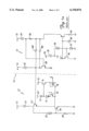
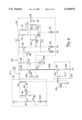
- FIG. 1A is a prior art circuit diagram showing a prior art preamplifier circuit.
- FIG. 1B is a prior art circuit diagram showing an individual channel circuit with use for a single strip magnetoresistive element.
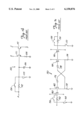
- FIG. 1C is a prior art circuit diagram showing an individual channel circuit for use with a dual strip magnetoresistive element.
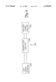
- FIG. 2 is a block diagram of a read system of the present invention.
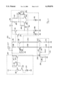
- FIG. 3 is a circuit diagram showing the present invention for use with a dual strip magnetoresistive element.
- FIG. 4 is a circuit diagram showing the present invention for use with a single strip magnetoresistive element.
- the present invention is a current bias, current sense preamplifier for use with one or more magnetoresistive (MR) read heads.
- the present invention provides a preamplifier which minimizes a DC signal during a read operation and minimizes the amount of unwanted noise within the preamplifier circuitry caused by MOSFET or jFET transistors in prior art designs.
- the DC signal is initially necessary to properly bias the MR reader such that it will read information from the magnetic storage medium.
- the present invention can be used in conjunction with a single or a dual strip MR head, and can be used with a single head or a plurality of heads.
- FIGS. 1A and 1B are circuit diagrams showing a prior art preamplifier circuit and a prior art individual channel circuit for use with a single strip MR head, respectively.
- FIGS. 1A and 1B can be coupled together in order to realize the multiplexed read out of information from a storage system.
- FIG. 1A shows prior art circuitry 50 which is common to all MR heads and
- FIG. 1B shows prior art circuitry 100 which is for an individual channel. While circuitry 100 is for an individual channel, multiple channels can be utilized by copying circuitry 100 as necessary.
- Feedback circuit 52 includes consist potential 56, current source 58, bi-polar junction transistor 60, diode 62, resistor 64, bi-polar junction transistor 66, consist potential 68, current source 70, diode 72, MOS transistor 74, bi-polar junction transistor 76, and MOS transistor 78.
- Preamplifier circuit 54 includes consist potential 56, current source 80, current source 82, bi-polar junction transistor 84, resistors 86 and 88, capacitor 90, current source 92, diode 94, bi-polar junction transistor 96, diode 97, capacitor 98, and resistor 99. Also shown in FIG. 1A are terminals A, B, C, and D. These terminals are the interconnection points between prior art circuitry 50 of FIG. 1A and prior art circuitry 100 of FIG. 1B.
- FIG. 1B shows prior art circuitry 100 which includes terminals A, B, C, and D, MR resistor 102, switches 104 and 105, DC blocking capacitor 106, resistor 108, and MOS transistors 110 and 112.
- MOS transistors 110 and 112 within individual channel circuitry 100 provide an unacceptable amount of noise which interferes with the reading of information from the magnetic storage medium by MR resistor 102 during a read operation.
- FIG. 1C is a prior art circuit diagram showing individual channel circuitry 150 for a balanced or dual version MR head.
- Circuitry 150 includes MR resistors 152 and 154, switches 156 and 158, MOS transistors 160, 162, 164, and 166, switches 168 and 170, resistors 172 and 174, and DC blocking capacitors 176 and 178.
- Circuitry 150 shown in FIG. 1C is virtually identical to circuitry 100 of FIG. 1B, except that circuitry 150 of FIG. 1C includes a second MR resistor and related circuitry. Therefore, the right side of FIG. 1C is the mirror image of the left side of FIG. 1C.
- One distinction between circuitry 150 of FIG. 1C and circuitry 100 of FIG. 1B is that rather than having DC blocking capacitor 106 of FIG. 1B connected to ground, DC blocking capacitors 176 and 178 of FIG. 1C are crossed coupled between the drain and source of MOS transistors 162 and 164. Similar to circuitry 100 shown in FIG. 1B, circuitry 150 of FIG. 1C suffers from unacceptably high noise due to MOS transistors 160, 162, 164, 166, thereby preventing MR resistors 152 and 154 from properly reading information from a magnetic storage medium during a read operation.
- FIG. 2 is a block diagram of a read system of the present invention.
- block diagram 200 includes bias current generator 202, preamplifier circuitry 204, and individual channel circuitry 206.
- the present invention lies within preamplifier 204 and individual channel circuitry 206 and utilizes at least one operational amplifier in a novel arrangement with at least one capacitor. This novel arrangement permits proper biasing of an MR head within individual channel circuitry 206 through use of a DC signal, while minimizing both the DC signal and unwanted noise during a read operation.
- Bias current generator 252 is a bias current generator system which will properly bias the head cell circuitry. However, it is understood that other designs for bias current generator 252 may be utilized in conjunction with the present invention. Voltage regulator 257 regulates the voltage within bias current generator 252 and preamplifier 256.
- Bias current generator 252 includes first potential V CC , second potential V EE , current source 258, transistors 260, 262, 264, and 265 and resistors 266 and 267.
- Transistors 260 and 262 are NPN bipolar junction transistors (BJTs), while transistors 264 and 265 are PNP BJTs.
- the collector of transistor 260 is connected to first voltage potential V CC , and the base of transistor 260 is connected to preamplifier circuitry 256.
- the emitter of transistor 260 is connected to the collector of transistor 262, while the emitter of transistor 262 is connected to current source 258, which is in turn connected to second voltage potential V EE .
- Resistor 266 is connected between preamplifier circuitry 256 and the emitter of transistor of 264.
- the collector of transistor 264 is connected to the base of transistor 264 and connected to the base of transistor 262.
- the base of transistor 264 is also connected to the base of transistor 265.
- Resistor 267 is connected between the emitter of transistor 265 and preamplifier circuitry 256.
- the collector of transistor 265 is connected to head cell circuitry 254 and to capacitor 280 of preamplifier circuitry 256.
- resistor 266 has a value in the range of 10 to 30 kilo Ohms, while resistor 267 has a value in the range of 5 to 20 kilo Ohms.
- Current source 258 should have a value in the range of 2 to 10 milliAmperes.
- Head cell circuitry 254 further includes MR resistors 268 and 270, PNP BJTs 272 and 274, and switch 276.
- MR resistors 268 and 270 are connected between the emitters of BJTs 272 and 274, respectively, and second voltage potential V EE .
- the bases of transistors 272 and 274 are interconnected and are also connected to switch 276.
- the collectors of BJTs 272 and 274 are connected via bus lines 278A and 278B to preamplifier circuitry 256.
- Switch 276 is connected to bias current generator 252 and preamplifier circuitry 256 via bus line 278C.
- MR resistors 268 and 270 should each have a value in the range of 5 to 100 Ohms.
- Preamplifier circuitry 256 utilizes two separate gain stages in order to provide a proper signal to external circuitries.
- the first stage includes capacitor 280, voltage source 282, resistors 284 and 286, BJTs 288, 290, 292, and 294, and current source generators 296 and 298.
- the second gain stage of preamplifier circuitry 256 includes resistors 300, 302, 304, and 306, BJTs 308 and 310, capacitors 312 and 314, current source 316, and voltage source 318.
- transistors 288, 290, 292, 294, 308, and 310 are all NPN BJTs.
- Voltage source 282 is connected between voltage potential V EE and the base of transistor 288.
- the base of transistor 288 is also connected to the base of transistor 290.
- Resistors 284 and 286 are connected between bias current generator 252 and the collector of transistors 288 and 290, respectively.
- the emitters of transistors 288 and 290 are connected to head cell circuitry 254 via bus lines 278B and 278A, respectively.
- Resistors 300 and 302 are connected between voltage potential V CC and the collector of transistors 308 and 310, respectively.
- Resistors 304 and 306 are connected between the bases of transistors 308 and 310 and voltage source 318, respectively.
- Current source 316 is connected to potential V EE .
- transistors 288 and 290 are cascode devices. The emitters of transistors 288 and 290 are the input points for all other individual head channels. Resistors 284 and 286 are the gain load resistors. The first stage gain is determined by dividing the value of resistor 284 by the value of resistor 268 or by dividing the value of resistor 286 by the value of resistor 270.
- the offset voltage of the first stage gain is eliminated by using two small capacitors 312 and 314 to AC-couple to the inputs of the second gain stage.
- the second gain stage consists of differential transistor pairs 308 and 310, load resistors 300 and 302, and tail current 316.
- capacitor 280 which is within preamplifier circuitry 256, has a value in the range of 25 to 500 picoFarrads, while capacitors 312 and 314 each have a value in the range of 10 to 250 picoFarrads.
- Resistors 284 and 286 should each have a value in the range of 100 to 750 Ohms, while current sources 296 and 298 should each have a value in the range of 0.25 to 3.0 milliAmperes.
- Voltage sources 282 and 318 should each have a value in the range of 0.5 to 5.0 volts.
- Resistors 300 and 302 should each have a value in the range of 250 to 3000 Ohms, while resistors 304 and 306 should each have a value in the range of 5.0 to 20.0 kilo Ohms.
- Current source 316 should have a value in the range of 1.0 to 5.0 milliAmperes.
Abstract
Description
Claims (18)
Priority Applications (1)
| Application Number | Priority Date | Filing Date | Title |
|---|---|---|---|
| US09/285,475 US6150876A (en) | 1998-04-06 | 1999-04-02 | Voltage bias, current sense preamplifier for a magnetoresistive reader |
Applications Claiming Priority (2)
| Application Number | Priority Date | Filing Date | Title |
|---|---|---|---|
| US8086998P | 1998-04-06 | 1998-04-06 | |
| US09/285,475 US6150876A (en) | 1998-04-06 | 1999-04-02 | Voltage bias, current sense preamplifier for a magnetoresistive reader |
Publications (1)
| Publication Number | Publication Date |
|---|---|
| US6150876A true US6150876A (en) | 2000-11-21 |
Family
ID=26764057
Family Applications (1)
| Application Number | Title | Priority Date | Filing Date |
|---|---|---|---|
| US09/285,475 Expired - Lifetime US6150876A (en) | 1998-04-06 | 1999-04-02 | Voltage bias, current sense preamplifier for a magnetoresistive reader |
Country Status (1)
| Country | Link |
|---|---|
| US (1) | US6150876A (en) |
Cited By (9)
| Publication number | Priority date | Publication date | Assignee | Title |
|---|---|---|---|---|
| US6583661B1 (en) * | 2000-11-03 | 2003-06-24 | Honeywell Inc. | Compensation mechanism for compensating bias levels of an operation circuit in response to supply voltage changes |
| US20030231419A1 (en) * | 2002-06-14 | 2003-12-18 | Takehiko Umeyama | Differential magneto-resistive head pre-amplifiers for single polarity power supply applications |
| US20040035941A1 (en) * | 2002-08-22 | 2004-02-26 | Indumini Ranmuthu | Preamplifier system having programmable resistance |
| US6738208B2 (en) | 2001-10-30 | 2004-05-18 | Seagate Technology Llc | Microwave noise testing circuit for a disc drive |
| US6822815B2 (en) | 2002-03-08 | 2004-11-23 | Seagate Technology Llc | Abnormal magnetoresistive element detection for a disc drive |
| US20060192617A1 (en) * | 2005-02-28 | 2006-08-31 | Barnett Raymond E | Low noise AC coupled amplifier with low band-pass corner and low power |
| US20070115575A1 (en) * | 2005-11-18 | 2007-05-24 | Cho Sung-Youn | Recording current optimization method of hard disk drive, recording medium storing program to execute the method and apparatus employing the same |
| US20070127149A1 (en) * | 2005-12-02 | 2007-06-07 | Texas Instruments Incorporated | Offset cancellation scheme for perpendicular reader |
| US20090212771A1 (en) * | 2008-02-27 | 2009-08-27 | John Cummings | Hysteresis offset cancellation for magnetic sensors |
Citations (3)
| Publication number | Priority date | Publication date | Assignee | Title |
|---|---|---|---|---|
| US5434717A (en) * | 1993-03-19 | 1995-07-18 | Hitachi, Ltd. | Read and/or write integrated circuit having an operation timing adjusting circuit and constant current elements |
| US5534818A (en) * | 1993-12-30 | 1996-07-09 | Vtc Inc. | Preamplifier noise filtering circuit |
| US5914630A (en) * | 1996-05-10 | 1999-06-22 | Vtc Inc. | MR head preamplifier with output signal amplitude which is independent of head resistance |
-
1999
- 1999-04-02 US US09/285,475 patent/US6150876A/en not_active Expired - Lifetime
Patent Citations (3)
| Publication number | Priority date | Publication date | Assignee | Title |
|---|---|---|---|---|
| US5434717A (en) * | 1993-03-19 | 1995-07-18 | Hitachi, Ltd. | Read and/or write integrated circuit having an operation timing adjusting circuit and constant current elements |
| US5534818A (en) * | 1993-12-30 | 1996-07-09 | Vtc Inc. | Preamplifier noise filtering circuit |
| US5914630A (en) * | 1996-05-10 | 1999-06-22 | Vtc Inc. | MR head preamplifier with output signal amplitude which is independent of head resistance |
Cited By (16)
| Publication number | Priority date | Publication date | Assignee | Title |
|---|---|---|---|---|
| US6583661B1 (en) * | 2000-11-03 | 2003-06-24 | Honeywell Inc. | Compensation mechanism for compensating bias levels of an operation circuit in response to supply voltage changes |
| US6738208B2 (en) | 2001-10-30 | 2004-05-18 | Seagate Technology Llc | Microwave noise testing circuit for a disc drive |
| US6822815B2 (en) | 2002-03-08 | 2004-11-23 | Seagate Technology Llc | Abnormal magnetoresistive element detection for a disc drive |
| US20030231419A1 (en) * | 2002-06-14 | 2003-12-18 | Takehiko Umeyama | Differential magneto-resistive head pre-amplifiers for single polarity power supply applications |
| US7187513B2 (en) | 2002-06-14 | 2007-03-06 | Renesas Technology America, Inc. | Differential magneto-resistive head pre-amplifiers for single polarity power supply applications |
| US20040035941A1 (en) * | 2002-08-22 | 2004-02-26 | Indumini Ranmuthu | Preamplifier system having programmable resistance |
| US7152800B2 (en) * | 2002-08-22 | 2006-12-26 | Texas Instruments Incorporated | Preamplifier system having programmable resistance |
| US7259624B2 (en) * | 2005-02-28 | 2007-08-21 | Texas Instruments Incorporated | Low noise AC coupled amplifier with low band-pass corner and low power |
| US20060192617A1 (en) * | 2005-02-28 | 2006-08-31 | Barnett Raymond E | Low noise AC coupled amplifier with low band-pass corner and low power |
| US20070115575A1 (en) * | 2005-11-18 | 2007-05-24 | Cho Sung-Youn | Recording current optimization method of hard disk drive, recording medium storing program to execute the method and apparatus employing the same |
| US7636213B2 (en) * | 2005-11-18 | 2009-12-22 | Samsung Electronics Co., Ltd | Recording current optimization method of hard disk drive, recording medium storing program to execute the method and apparatus employing the same |
| US20070127149A1 (en) * | 2005-12-02 | 2007-06-07 | Texas Instruments Incorporated | Offset cancellation scheme for perpendicular reader |
| US20090212771A1 (en) * | 2008-02-27 | 2009-08-27 | John Cummings | Hysteresis offset cancellation for magnetic sensors |
| WO2009108420A1 (en) * | 2008-02-27 | 2009-09-03 | Allegro Microsystems, Inc. | Hysteresis offset cancellation for magnetic sensors |
| US8269491B2 (en) | 2008-02-27 | 2012-09-18 | Allegro Microsystems, Inc. | DC offset removal for a magnetic field sensor |
| US9046562B2 (en) | 2008-02-27 | 2015-06-02 | Allegro Microsystems, Llc | Hysteresis offset cancellation for magnetic sensors |
Similar Documents
| Publication | Publication Date | Title |
|---|---|---|
| US5270882A (en) | Low-voltage, low-power amplifier for magnetoresistive sensor | |
| US7082004B2 (en) | Disk storage systems | |
| US5619386A (en) | Arrangement for reading information from a track on a record carrier comprising a fast settling read amplifier for magneto-resistive heads | |
| US7190541B2 (en) | Hi-speed preamplifier write driver for hard drive with improved symmetry | |
| US6150876A (en) | Voltage bias, current sense preamplifier for a magnetoresistive reader | |
| US5345346A (en) | Positive feedback low input capacitance differential amplifier | |
| EP0764320B1 (en) | Arrangement comprising a magnetic write head, and write amplifier with capacitive current compensation | |
| US5691663A (en) | Single-ended supply preamplifier with high power supply rejection ratio | |
| US5668676A (en) | Magnetic head write amplifier including current mirrors and switchable current sources | |
| US6226137B1 (en) | Voltage bias, current sense preamplifier using no AC-coupling capacitors for a dual strip magnetoresistive reader | |
| US6275347B1 (en) | Current bias, current sense preamplifier for a magnetoresistive reader | |
| US5831784A (en) | Pseudo differential voltage sense MR preamplifier with improved bandwidth | |
| US6066987A (en) | Differential cascode magneto-resistance preamplifier with bias bypass | |
| US6219194B1 (en) | MR head read amplifier with improved write to read recovery time | |
| US6107873A (en) | Low noise common-emitter preamplifier for magneto-resistive heads | |
| US7564638B2 (en) | Preamplifier circuit and method for a disk drive device | |
| EP0459579B1 (en) | Read head arrangement comprising 2n read heads of the MR type, and reproduction arrangement comprising the read head arrangement | |
| US5543979A (en) | Preamplifier circuit arrangements for common current flow in a transducer | |
| US6211736B1 (en) | Signal amplifying circuit for magnetoresistive element | |
| US6538832B1 (en) | Single ended preamplifier having multiple first stage banks for improved noise characteristics | |
| KR20000062710A (en) | Readback amplifier for wideband readout of magneto-resistive heads for data storage | |
| US6967525B2 (en) | Tail current generator circuit for bipolar/MOS differential pair to set precise transconductance | |
| US20020047734A1 (en) | Driving circuit for a voice coil motor and driving method thereof | |
| KR20010021945A (en) | Recording apparatus provided with a write driver circuit | |
| US7209307B2 (en) | Variable read output impedance control circuit for a magnetic media storage system |
Legal Events
| Date | Code | Title | Description |
|---|---|---|---|
| AS | Assignment |
Owner name: VTC INC., MINNESOTA Free format text: ASSIGNMENT OF ASSIGNORS INTEREST;ASSIGNOR:NGO, TUAN V.;REEL/FRAME:009882/0433 Effective date: 19990401 |
|
| AS | Assignment |
Owner name: LUCENT TECHNOLOGIES INC., NEW JERSEY Free format text: ASSIGNMENT OF ASSIGNORS INTEREST;ASSIGNOR:VTC INC.;REEL/FRAME:010906/0515 Effective date: 20000203 |
|
| STCF | Information on status: patent grant |
Free format text: PATENTED CASE |
|
| FEPP | Fee payment procedure |
Free format text: PAYOR NUMBER ASSIGNED (ORIGINAL EVENT CODE: ASPN); ENTITY STATUS OF PATENT OWNER: LARGE ENTITY |
|
| FEPP | Fee payment procedure |
Free format text: PAYER NUMBER DE-ASSIGNED (ORIGINAL EVENT CODE: RMPN); ENTITY STATUS OF PATENT OWNER: LARGE ENTITY Free format text: PAYOR NUMBER ASSIGNED (ORIGINAL EVENT CODE: ASPN); ENTITY STATUS OF PATENT OWNER: LARGE ENTITY |
|
| FPAY | Fee payment |
Year of fee payment: 4 |
|
| FPAY | Fee payment |
Year of fee payment: 8 |
|
| FPAY | Fee payment |
Year of fee payment: 12 |
|
| AS | Assignment |
Owner name: DEUTSCHE BANK AG NEW YORK BRANCH, AS COLLATERAL AG Free format text: PATENT SECURITY AGREEMENT;ASSIGNORS:LSI CORPORATION;AGERE SYSTEMS LLC;REEL/FRAME:032856/0031 Effective date: 20140506 |
|
| AS | Assignment |
Owner name: AVAGO TECHNOLOGIES GENERAL IP (SINGAPORE) PTE. LTD Free format text: ASSIGNMENT OF ASSIGNORS INTEREST;ASSIGNOR:AGERE SYSTEMS LLC;REEL/FRAME:035365/0634 Effective date: 20140804 |
|
| AS | Assignment |
Owner name: LSI CORPORATION, CALIFORNIA Free format text: TERMINATION AND RELEASE OF SECURITY INTEREST IN PATENT RIGHTS (RELEASES RF 032856-0031);ASSIGNOR:DEUTSCHE BANK AG NEW YORK BRANCH, AS COLLATERAL AGENT;REEL/FRAME:037684/0039 Effective date: 20160201 Owner name: AGERE SYSTEMS LLC, PENNSYLVANIA Free format text: TERMINATION AND RELEASE OF SECURITY INTEREST IN PATENT RIGHTS (RELEASES RF 032856-0031);ASSIGNOR:DEUTSCHE BANK AG NEW YORK BRANCH, AS COLLATERAL AGENT;REEL/FRAME:037684/0039 Effective date: 20160201 |
|
| AS | Assignment |
Owner name: BANK OF AMERICA, N.A., AS COLLATERAL AGENT, NORTH CAROLINA Free format text: PATENT SECURITY AGREEMENT;ASSIGNOR:AVAGO TECHNOLOGIES GENERAL IP (SINGAPORE) PTE. LTD.;REEL/FRAME:037808/0001 Effective date: 20160201 Owner name: BANK OF AMERICA, N.A., AS COLLATERAL AGENT, NORTH Free format text: PATENT SECURITY AGREEMENT;ASSIGNOR:AVAGO TECHNOLOGIES GENERAL IP (SINGAPORE) PTE. LTD.;REEL/FRAME:037808/0001 Effective date: 20160201 |
|
| AS | Assignment |
Owner name: AVAGO TECHNOLOGIES GENERAL IP (SINGAPORE) PTE. LTD., SINGAPORE Free format text: TERMINATION AND RELEASE OF SECURITY INTEREST IN PATENTS;ASSIGNOR:BANK OF AMERICA, N.A., AS COLLATERAL AGENT;REEL/FRAME:041710/0001 Effective date: 20170119 Owner name: AVAGO TECHNOLOGIES GENERAL IP (SINGAPORE) PTE. LTD Free format text: TERMINATION AND RELEASE OF SECURITY INTEREST IN PATENTS;ASSIGNOR:BANK OF AMERICA, N.A., AS COLLATERAL AGENT;REEL/FRAME:041710/0001 Effective date: 20170119 |
|
| AS | Assignment |
Owner name: AVAGO TECHNOLOGIES INTERNATIONAL SALES PTE. LIMITE Free format text: ASSIGNMENT OF ASSIGNORS INTEREST;ASSIGNOR:AVAGO TECHNOLOGIES GENERAL IP (SINGAPORE) PTE. LTD.;REEL/FRAME:047022/0620 Effective date: 20180509 |
|
| AS | Assignment |
Owner name: AVAGO TECHNOLOGIES INTERNATIONAL SALES PTE. LIMITE Free format text: CORRECTIVE ASSIGNMENT TO CORRECT THE NATURE OF CONVEYANCE AND EFFECTIVE DATE PREVIOUSLY RECORDED ON REEL 047022 FRAME 0620. ASSIGNOR(S) HEREBY CONFIRMS THE MERGER;ASSIGNOR:AVAGO TECHNOLOGIES GENERAL IP (SINGAPORE) PTE. LTD.;REEL/FRAME:047185/0643 Effective date: 20180509 |
|
| AS | Assignment |
Owner name: AVAGO TECHNOLOGIES INTERNATIONAL SALES PTE. LIMITE Free format text: CORRECTIVE ASSIGNMENT TO CORRECT THE EFFECTIVE DATE PREVIOUSLY RECORDED ON REEL 047185 FRAME 0643. ASSIGNOR(S) HEREBY CONFIRMS THE MERGER;ASSIGNOR:AVAGO TECHNOLOGIES GENERAL IP (SINGAPORE) PTE. LTD.;REEL/FRAME:047476/0845 Effective date: 20180905 |
|
| AS | Assignment |
Owner name: AVAGO TECHNOLOGIES INTERNATIONAL SALES PTE. LIMITE Free format text: CORRECTIVE ASSIGNMENT TO CORRECT THE EFFECTIVE DATE OF MERGER PREVIOUSLY RECORDED AT REEL: 047185 FRAME: 0643. ASSIGNOR(S) HEREBY CONFIRMS THE CORRECTIVE MERGER;ASSIGNOR:AVAGO TECHNOLOGIES GENERAL IP (SINGAPORE) PTE. LTD.;REEL/FRAME:047959/0296 Effective date: 20180905 |