US6150748A - Surface-acoustic-wave device - Google Patents
Surface-acoustic-wave device Download PDFInfo
- Publication number
- US6150748A US6150748A US09/241,015 US24101599A US6150748A US 6150748 A US6150748 A US 6150748A US 24101599 A US24101599 A US 24101599A US 6150748 A US6150748 A US 6150748A
- Authority
- US
- United States
- Prior art keywords
- acoustic
- conductive film
- wave element
- grounding means
- sections
- Prior art date
- Legal status (The legal status is an assumption and is not a legal conclusion. Google has not performed a legal analysis and makes no representation as to the accuracy of the status listed.)
- Expired - Fee Related
Links
Images


Classifications
-
- H—ELECTRICITY
- H03—ELECTRONIC CIRCUITRY
- H03H—IMPEDANCE NETWORKS, e.g. RESONANT CIRCUITS; RESONATORS
- H03H9/00—Networks comprising electromechanical or electro-acoustic devices; Electromechanical resonators
- H03H9/02—Details
- H03H9/05—Holders; Supports
- H03H9/10—Mounting in enclosures
- H03H9/1064—Mounting in enclosures for surface acoustic wave [SAW] devices
- H03H9/1078—Mounting in enclosures for surface acoustic wave [SAW] devices the enclosure being defined by a foil covering the non-active sides of the SAW device
-
- H—ELECTRICITY
- H03—ELECTRONIC CIRCUITRY
- H03H—IMPEDANCE NETWORKS, e.g. RESONANT CIRCUITS; RESONATORS
- H03H9/00—Networks comprising electromechanical or electro-acoustic devices; Electromechanical resonators
- H03H9/02—Details
- H03H9/05—Holders; Supports
- H03H9/058—Holders; Supports for surface acoustic wave devices
- H03H9/059—Holders; Supports for surface acoustic wave devices consisting of mounting pads or bumps
-
- H—ELECTRICITY
- H03—ELECTRONIC CIRCUITRY
- H03H—IMPEDANCE NETWORKS, e.g. RESONANT CIRCUITS; RESONATORS
- H03H9/00—Networks comprising electromechanical or electro-acoustic devices; Electromechanical resonators
- H03H9/02—Details
- H03H9/05—Holders; Supports
- H03H9/10—Mounting in enclosures
- H03H9/1064—Mounting in enclosures for surface acoustic wave [SAW] devices
- H03H9/1071—Mounting in enclosures for surface acoustic wave [SAW] devices the enclosure being defined by a frame built on a substrate and a cap, the frame having no mechanical contact with the SAW device
-
- H—ELECTRICITY
- H01—ELECTRIC ELEMENTS
- H01L—SEMICONDUCTOR DEVICES NOT COVERED BY CLASS H10
- H01L2224/00—Indexing scheme for arrangements for connecting or disconnecting semiconductor or solid-state bodies and methods related thereto as covered by H01L24/00
- H01L2224/01—Means for bonding being attached to, or being formed on, the surface to be connected, e.g. chip-to-package, die-attach, "first-level" interconnects; Manufacturing methods related thereto
- H01L2224/10—Bump connectors; Manufacturing methods related thereto
- H01L2224/15—Structure, shape, material or disposition of the bump connectors after the connecting process
- H01L2224/16—Structure, shape, material or disposition of the bump connectors after the connecting process of an individual bump connector
- H01L2224/161—Disposition
- H01L2224/16151—Disposition the bump connector connecting between a semiconductor or solid-state body and an item not being a semiconductor or solid-state body, e.g. chip-to-substrate, chip-to-passive
- H01L2224/16221—Disposition the bump connector connecting between a semiconductor or solid-state body and an item not being a semiconductor or solid-state body, e.g. chip-to-substrate, chip-to-passive the body and the item being stacked
- H01L2224/16225—Disposition the bump connector connecting between a semiconductor or solid-state body and an item not being a semiconductor or solid-state body, e.g. chip-to-substrate, chip-to-passive the body and the item being stacked the item being non-metallic, e.g. insulating substrate with or without metallisation
-
- H—ELECTRICITY
- H01—ELECTRIC ELEMENTS
- H01L—SEMICONDUCTOR DEVICES NOT COVERED BY CLASS H10
- H01L2924/00—Indexing scheme for arrangements or methods for connecting or disconnecting semiconductor or solid-state bodies as covered by H01L24/00
- H01L2924/15—Details of package parts other than the semiconductor or other solid state devices to be connected
- H01L2924/161—Cap
- H01L2924/1615—Shape
- H01L2924/16195—Flat cap [not enclosing an internal cavity]
Definitions
- the present invention relates to a surface-acoustic-wave device (hereinafter, referred to as a SAW device).
- a SAW device having a SAW element on which interdigital electrodes are formed and which is covered with a conductive thin-film to shield the SAW element against an external electric field.
- FIG. 1 represents an example of construction of a SAW device currently in use.
- Interdigital electrodes 2 and I/O (input/output) electrodes 3-1, 3-2 are formed of aluminum (Al) thin films on one surface of a SAW element 1.
- SAW element 1 is formed on ceramic substrate 11 with interposition of ground pattern 8.
- I/O terminals 10-1 and 10-2 are formed on ceramic substrate 11.
- I/O electrode 4-1 is connected with I/O terminal 10-1 via through-hole 9-1.
- I/O electrode 4-2 is connected with I/O terminal 10-2 via through-hole 9-2.
- Seam-ring 6 and metal cover 7 define a space above the surface on which interdigital electrodes of the SAW device are formed.
- FIG. 2 shows another example of a SAW device in which metal bumps 21-1, 21-2 are employed to perform an electric I/O between SAW element 1 and an external circuit.
- interdigital electrodes 2 and I/O electrodes 3-1, 3-2 are formed on one surface (a first surface) of SAW element 1.
- the I/O electrode 3-1 of SAW element 1 is connected with I/O electrode 4-1 through metal bump 21-1.
- I/O electrode 4-1 is formed on the surface of ceramic substrate 11.
- the I/O electrode 3-2 is connected with I/O electrode 4-2, formed on the surface of ceramic substrate 11, through metal bump 21-2.
- a ground pattern 8 is formed on one of the surfaces of ceramic substrate 11 where I/O electrodes 4-1, 4-2 are provided. I/O terminals 10-1, 10-2 are formed on the opposite surface of the substrate.
- I/O terminal 10-1 and I/O electrode 4-1 are connected through through-hole 9-1, and, similarly, I/O terminal 10-2 and I/O electrode 4-2 are connected through through-hole 9-2.
- SAW element 1 is surrounded with seam-ring 6 and metal cover 7.
- This mounting method includes a problem concerning the way of preventing an erosion of an Al pattern formed on a surface of a SAW element (the pattern of the interdigital electrodes).
- the method includes another problem to be taken into account concerning the way of electric-shielding of the SAW element against an external electric field neither giving rise to a high cost nor enlarging the volume of the SAW device.
- a protective layer for example SiO 2 .
- a first surface-acoustic-wave device (a first SAW device) has a surface-acoustic-wave element provided with interdigital electrodes, a shut-off member and ground patterns.
- the SAW device is mounted on a mounting substrate.
- the interdigital electrodes are formed on a first surface of the surface-acoustic-wave element.
- the shut-off member serves to shut off the surface-acoustic-wave element electrically and airtightly from an ambience.
- the ground patterns are electrically grounded to discharge an electric charge.
- the ground patterns have sections mounted on a surface of the mounting substrate.
- the shut-off member covers the SAW element and also contacts the sections of the grounding patterns.
- the shut-off member is preferably applied on the surface-acoustic-wave element so as to cover a second surface opposite to the first surface and also side surfaces of the surface-acoustic-wave element.
- both end-portions of the shut-off member are electrically and mechanically attached to the sections of the grounding patterns mounted on the surface of the mounting substrate.
- the shut-off member is preferably formed of a conductive film.
- the shut-off member and each of the sections of the ground patterns are preferably connected with each other through a conductive resin member.
- the shut-off member and each of the sections of the ground patterns are preferably connected with each other through a conductive adhesive material.
- shut-off member The end portions of the shut-off member are preferably bent inward to connect with the ground pattern.
- shut-off member The end portions of the shut-off member are preferably bent outward to connect with the ground pattern.
- a second surface-acoustic-wave device has a surface-acoustic-wave element provided with interdigital electrodes, a shut-off member and ground patterns.
- the interdigital electrodes are formed on a first surface of the surface-acoustic-wave element.
- the shut-off member serves to shut off the surface-acoustic-wave element electrically and airtightly from an ambience.
- the ground patterns are electrically grounded to discharge an electric charge and also have sections mounted on a surface of the mounting substrate.
- the surface-acoustic-wave element is embedded in a recess made in the mounting substrate.
- the shut-off member covering the surface-acoustic-wave element, contacts the sections of the ground patterns mounted on the surface of the mounting substrate.
- the mounting substrate is a multiple-layer substrate, and that the recess is a hole opened through a first layer.
- a second surface opposite to the first surface of the surface-acoustic-wave element is arranged to be flush with a surface of the first layer of the multiple-layer substrate.
- the shut-off member contacts the sections of the ground patterns in such a manner that the shut-off member covers both the second surface of the surface-acoustic-wave element and the sections mounted on the surface of the first layer of the multiple-layer substrate.
- the first and second SAW devices configured as described above enable to perform electrical shielding of the SAW element against an external electric field while designed to be of a low cost and a simple construction as well as a small volume.
- FIG. 1 is a cross-sectional view of a first example of a SAW device currently in use.
- FIG. 2 is a cross-sectional view of a second example of a SAW device currently in use.
- FIG. 3 is a cross-sectional view of a first embodiment of the SAW device according to the present invention illustrating the construction thereof.
- FIG. 4 is a plan view of the SAW device according to the present embodiment as viewed from the topside.
- FIG. 5 is a cross-sectional view of the SAW device in the second embodiment.
- FIG. 6 is a cross-sectional view of the SAW device in the third embodiment.
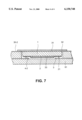
- FIG. 7 is a cross-sectional view of the SAW device in the fourth embodiment.
- FIG. 3 is a cross-sectional view of a first embodiment of the SAW device according to the present invention illustrating the construction thereof.
- interdigital electrode 2 and I/O electrodes 3-1, 3-2 are formed of Al thin-films on one of the surfaces, or a first surface, of SAW element 1.
- I/O electrodes 3-1, 3-2 are generically referred to as I/O electrodes 3.
- the end sections of the first surface (the surface provided with interdigital electrodes) and the entire surface of the second surface opposite to the first surface are covered with Al thin-films 31. Furthermore, a sheet of conductive film 32 encloses allover the Al thin-films 31 and side surfaces of SAW element 1.
- Interdigital electrode 2 is covered with a protective layer such as SiO 2 .
- I/O electrode 3-1 is connected electrically and mechanically with I/O electrode 4-1 by means of metal bump 21-1.
- I/O electrode 3-2 is connected electrically and mechanically with I/O electrode 4-2 by means of metal bump 21-2.
- Conductive film 32 has a thermocrimping property (property of connecting a material with other material under heat and pressure). With the aid of this property, contacts between conductive film 32 and SAW element 1 as well as between conductive film 32 and ground electrode 35-1, 35-2 formed on print substrate 36 can be made at the same time. The contact is carried out using the heat and pressure applied when SAW element 1 is bump-bonded with print substrate 36.
- Resin member 34 is formed on SAW element 1 surrounding interdigital electrode 2.
- the resin member 34 ensures a spacing of SAW element 1 from printing substrate 36.
- the space enclosed by SAW element 1, print substrate 36 and resin member 34 makes a chamber airtight from the ambience.
- FIG. 3 represents only two of I/O electrodes 3-1, 3-2 and metal bumps 21-1, 21-2, respectively, actually four I/O electrodes and four metal bumps are provided, as is shown in FIG. 4.
- FIG. 3 represents one interdigital electrode 2, actually two interdigital electrodes are provided.
- FIG. 4 is a plan view of the SAW device according to the present embodiment as viewed from the topside.
- interdigital electrodes 2 and I/O electrodes 3 for SAW element 1, metal bumps 21, and the patterns on print substrate 36, i.e., output pattern 41, input pattern 42, ground patterns 42-1, 43-2, are shown in a transparent view by broken lines.
- An electric signal applied across input patterns 42 and 43-2 is transferred to I/O electrodes 3-3, 3-4 through metal bumps 21-3, 21-4 and transduced into a SAW at interdigital electrodes 2-2.
- the SAW upon reaching interdigital electrodes 2-1, is transduced into an electric signal that appears across I/O electrodes 3-1, 3-2.
- the electric signal is transferred from I/O electrode 3-1,3-2 to output patterns 41, 43-1 through metal bumps 21-1, 21-2.
- the electric characteristics of the output electric signal relative to the input electric signal substantially depend on the shape of interdigital electrodes 2-1, 2-2.
- electrically grounded conductive film 32 covers the entirety of input pattern 42, output pattern 41, I/O electrodes 3-1 through 3-4, metal bump 21-1 through 21-4 and interdigital electrodes 2-1, 2-2.
- the conductive film 32 serves to shield the essential part of the device electrically against an external electric field.
- the present embodiment can offer a SAW device shielded against an external noise field
- conductive film 32 can serve as a kind of a protective wall against an external impact, the present embodiment allows relieving an external impact force acting on the SAW device.
- FIGS. 5-7 the same parts as those in FIGS. 3 and 4 are labeled with same reference numbers as denoted in FIGS. 3 and 4.
- conductive resin member 51 is used to combine conductive film 32 with ground electrode 35 provided on the surface of print substrate 51 like the device shown in FIG. 3.
- Conductive adhesive material may be employed in lieu of conductive resin member 51. Explanation concerning other constituent elements of the device and the operation thereof will be omitted for simplicity, because they are similar to those already set forth with reference to FIG. 3.
- the SAW device of the second embodiment enables to attain similar technical effects to those of the first embodiment.
- conductive film 32 is bent externally to combine with ground electrode 35 formed, like the device shown in FIG. 3, on the surface of print substrate 51.
- FIG. 7 is a cross-sectional view of a fourth embodiment of the present invention.
- multiple-layer print substrate 61 is employed.
- the first layer of the substrate 61 has a through-hole in which SAW element 1 is received.
- the first layer of multiple-layer substrate 61 surrounds SAW element 1.
- a second surface of SAW element 1, which is opposite to the first surface provided with interdigital electrode 2, is substantially flush with the surface of the substrate 61 on which ground electrodes 35 are formed (the surface of the first layer of the substrate 61).
- Conductive film 32 is formed so as to cover both the entirety of the second surface of SAW element 1 and at least a part of ground electrode 35 formed on the surface of the first layer of the substrate 61. In this way, SAW element 1 is shut off electrically and airtightly from ambience.
- conductive film 32 is employed in the above-described embodiments, any conductive member may be used in lieu of the conductive film.
Abstract
Description
Claims (8)
Applications Claiming Priority (2)
| Application Number | Priority Date | Filing Date | Title |
|---|---|---|---|
| JP10-054127 | 1998-02-20 | ||
| JP10054127A JPH11239037A (en) | 1998-02-20 | 1998-02-20 | Surface acoustic wave device |
Publications (1)
| Publication Number | Publication Date |
|---|---|
| US6150748A true US6150748A (en) | 2000-11-21 |
Family
ID=12961937
Family Applications (1)
| Application Number | Title | Priority Date | Filing Date |
|---|---|---|---|
| US09/241,015 Expired - Fee Related US6150748A (en) | 1998-02-20 | 1999-02-01 | Surface-acoustic-wave device |
Country Status (4)
| Country | Link |
|---|---|
| US (1) | US6150748A (en) |
| JP (1) | JPH11239037A (en) |
| CN (1) | CN1130015C (en) |
| GB (1) | GB2334618B (en) |
Cited By (26)
| Publication number | Priority date | Publication date | Assignee | Title |
|---|---|---|---|---|
| EP1241783A1 (en) * | 2001-03-14 | 2002-09-18 | Murata Manufacturing Co., Ltd. | Surface acoustic wave device and communications apparatus including the same |
| US20030146677A1 (en) * | 2001-12-18 | 2003-08-07 | Toshiyuki Baba | Surface acoustic wave device |
| US6734601B2 (en) * | 2001-04-10 | 2004-05-11 | Murata Manufacturing Co., Ltd. | Surface acoustic wave device, method for making the same, and communication apparatus including the same |
| US20040103509A1 (en) * | 1998-12-08 | 2004-06-03 | Agnes Bidard | Encapsulated surface acoustic wave component and method of collective fabrication |
| US20050062167A1 (en) * | 2003-09-24 | 2005-03-24 | Yu-Tung Huang | Package assembly for electronic device and method of making same |
| US20050116352A1 (en) * | 2003-11-14 | 2005-06-02 | Suguru Warashina | Acoustic wave device and method of fabricating the same |
| US20060113874A1 (en) * | 2004-11-05 | 2006-06-01 | Chi-Yen Shen | Surface acoustic wave device package |
| US20060170089A1 (en) * | 2005-01-31 | 2006-08-03 | Fujitsu Limited | Electronic device and method for fabricating the same |
| US20100181868A1 (en) * | 2008-12-17 | 2010-07-22 | Sand9, Inc. | Multi-port mechanical resonating devices and related methods |
| US20110148531A1 (en) * | 2009-12-23 | 2011-06-23 | Sand9, Inc. | Oscillators having arbitrary frequencies and related systems and methods |
| US20110181366A1 (en) * | 2009-12-23 | 2011-07-28 | Sand9, Inc. | Oscillators having arbitrary frequencies and related systems and methods |
| US8362675B2 (en) | 2008-12-17 | 2013-01-29 | Sand 9, Inc. | Mechanical resonating structures including a temperature compensation structure |
| US20130187730A1 (en) * | 2012-01-24 | 2013-07-25 | Taiyo Yuden Co., Ltd. | Acoustic wave device and fabrication method of the same |
| US8704604B2 (en) | 2009-12-23 | 2014-04-22 | Sand 9, Inc. | Oscillators having arbitrary frequencies and related systems and methods |
| DE10164494B4 (en) * | 2001-12-28 | 2014-06-18 | Epcos Ag | Encapsulated low-profile device and method of manufacture |
| US9006880B1 (en) | 2000-11-28 | 2015-04-14 | Knowles Electronics, Llc | Top port multi-part surface mount silicon condenser microphone |
| US9040360B1 (en) | 2000-11-28 | 2015-05-26 | Knowles Electronics, Llc | Methods of manufacture of bottom port multi-part surface mount MEMS microphones |
| US9078063B2 (en) | 2012-08-10 | 2015-07-07 | Knowles Electronics, Llc | Microphone assembly with barrier to prevent contaminant infiltration |
| US9173315B2 (en) * | 2005-11-09 | 2015-10-27 | Koninklijke Philips N.V. | Package carrier for a microelectronic element |
| EP1482638B1 (en) * | 2003-05-29 | 2016-01-13 | Samsung Electronics Co., Ltd. | Film bulk acoustic resonator having supports and manufacturing method therefor |
| US9374643B2 (en) | 2011-11-04 | 2016-06-21 | Knowles Electronics, Llc | Embedded dielectric as a barrier in an acoustic device and method of manufacture |
| US9654081B2 (en) | 2013-07-17 | 2017-05-16 | Murata Manufacturing Co., Ltd. | Electronic component and manufacturing method therefor |
| US9762202B2 (en) | 2008-12-17 | 2017-09-12 | Analog Devices, Inc. | Method of manufacturing a mechanical resonating structure |
| US9794661B2 (en) | 2015-08-07 | 2017-10-17 | Knowles Electronics, Llc | Ingress protection for reducing particle infiltration into acoustic chamber of a MEMS microphone package |
| US10800649B2 (en) | 2016-11-28 | 2020-10-13 | Analog Devices International Unlimited Company | Planar processing of suspended microelectromechanical systems (MEMS) devices |
| US10843920B2 (en) | 2019-03-08 | 2020-11-24 | Analog Devices International Unlimited Company | Suspended microelectromechanical system (MEMS) devices |
Families Citing this family (6)
| Publication number | Priority date | Publication date | Assignee | Title |
|---|---|---|---|---|
| JP2000058593A (en) * | 1998-08-03 | 2000-02-25 | Nec Corp | Mounting structure of surface elastic wave element and mounting thereof |
| JP2004201285A (en) * | 2002-12-06 | 2004-07-15 | Murata Mfg Co Ltd | Method of producing piezoelectric component and piezoelectric component |
| JP4881337B2 (en) * | 2008-03-12 | 2012-02-22 | ルネサスエレクトロニクス株式会社 | Semiconductor device |
| JP5786812B2 (en) * | 2012-07-11 | 2015-09-30 | 株式会社村田製作所 | Electronic component and manufacturing method thereof |
| CN104330470B (en) * | 2014-09-30 | 2018-04-10 | 成都柏森松传感技术有限公司 | Detection means based on SAW sensor |
| CN113054092B (en) * | 2021-06-01 | 2021-08-24 | 绍兴中芯集成电路制造股份有限公司 | Device and packaging method thereof |
Citations (12)
| Publication number | Priority date | Publication date | Assignee | Title |
|---|---|---|---|---|
| JPS60199929A (en) * | 1984-03-26 | 1985-10-09 | Tsuzuki Boeki Kk | Method for doffing in spinning machine and apparatus therefor |
| JPS61202508A (en) * | 1985-03-06 | 1986-09-08 | Matsushima Kogyo Co Ltd | Piezoelectric vibrator |
| JPH03173216A (en) * | 1989-12-01 | 1991-07-26 | Matsushita Electric Ind Co Ltd | Surface acoustic wave device |
| EP0637871A1 (en) * | 1993-08-06 | 1995-02-08 | Matsushita Electric Industrial Co., Ltd. | Surface acoustic wave device mounted module |
| US5699027A (en) * | 1995-03-28 | 1997-12-16 | Matsushita Electric Industrial Co., Ltd. | Surface acoustic wave devices having a guard layer |
| US5712523A (en) * | 1995-01-11 | 1998-01-27 | Murata Manufacturing Co., Ltd. | Surface acoustic wave device |
| EP0840369A1 (en) * | 1995-06-30 | 1998-05-06 | Kabushiki Kaisha Toshiba | Electronic component and method of production thereof |
| US5818145A (en) * | 1995-04-10 | 1998-10-06 | Nec Corporation | Surface acoustic wave device |
| US5821665A (en) * | 1995-05-08 | 1998-10-13 | Matsushita Electric Industrial Co., Ltd. | Surface acoustic wave device and method of manufacture |
| EP0896427A2 (en) * | 1997-08-05 | 1999-02-10 | Nec Corporation | Surface acoustic wave device |
| US5939817A (en) * | 1994-09-22 | 1999-08-17 | Nippon Electric Co | Surface acoustic wave device |
| US6033852A (en) * | 1996-09-27 | 2000-03-07 | University Of Maine | Monolithic piezoelectric sensor (MPS) for sensing chemical, biochemical and physical measurands |
-
1998
- 1998-02-20 JP JP10054127A patent/JPH11239037A/en active Pending
-
1999
- 1999-02-01 US US09/241,015 patent/US6150748A/en not_active Expired - Fee Related
- 1999-02-10 GB GB9903018A patent/GB2334618B/en not_active Expired - Fee Related
- 1999-02-20 CN CN99102233A patent/CN1130015C/en not_active Expired - Fee Related
Patent Citations (14)
| Publication number | Priority date | Publication date | Assignee | Title |
|---|---|---|---|---|
| JPS60199929A (en) * | 1984-03-26 | 1985-10-09 | Tsuzuki Boeki Kk | Method for doffing in spinning machine and apparatus therefor |
| JPS61202508A (en) * | 1985-03-06 | 1986-09-08 | Matsushima Kogyo Co Ltd | Piezoelectric vibrator |
| JPH03173216A (en) * | 1989-12-01 | 1991-07-26 | Matsushita Electric Ind Co Ltd | Surface acoustic wave device |
| EP0637871A1 (en) * | 1993-08-06 | 1995-02-08 | Matsushita Electric Industrial Co., Ltd. | Surface acoustic wave device mounted module |
| US5459368A (en) * | 1993-08-06 | 1995-10-17 | Matsushita Electric Industrial Co., Ltd. | Surface acoustic wave device mounted module |
| US5939817A (en) * | 1994-09-22 | 1999-08-17 | Nippon Electric Co | Surface acoustic wave device |
| US5712523A (en) * | 1995-01-11 | 1998-01-27 | Murata Manufacturing Co., Ltd. | Surface acoustic wave device |
| US5699027A (en) * | 1995-03-28 | 1997-12-16 | Matsushita Electric Industrial Co., Ltd. | Surface acoustic wave devices having a guard layer |
| US5818145A (en) * | 1995-04-10 | 1998-10-06 | Nec Corporation | Surface acoustic wave device |
| US5821665A (en) * | 1995-05-08 | 1998-10-13 | Matsushita Electric Industrial Co., Ltd. | Surface acoustic wave device and method of manufacture |
| US5991989A (en) * | 1995-05-08 | 1999-11-30 | Matsushita Electric Industrial Co., Ltd. | Method of manufacture of surface acoustic wave device |
| EP0840369A1 (en) * | 1995-06-30 | 1998-05-06 | Kabushiki Kaisha Toshiba | Electronic component and method of production thereof |
| US6033852A (en) * | 1996-09-27 | 2000-03-07 | University Of Maine | Monolithic piezoelectric sensor (MPS) for sensing chemical, biochemical and physical measurands |
| EP0896427A2 (en) * | 1997-08-05 | 1999-02-10 | Nec Corporation | Surface acoustic wave device |
Cited By (56)
| Publication number | Priority date | Publication date | Assignee | Title |
|---|---|---|---|---|
| US20040103509A1 (en) * | 1998-12-08 | 2004-06-03 | Agnes Bidard | Encapsulated surface acoustic wave component and method of collective fabrication |
| US6852561B2 (en) | 1998-12-08 | 2005-02-08 | Thomson-Csf | Encapsulated surface acoustic wave component and method of collective fabrication |
| US9156684B1 (en) | 2000-11-28 | 2015-10-13 | Knowles Electronics, Llc | Methods of manufacture of top port surface mount MEMS microphones |
| US9067780B1 (en) | 2000-11-28 | 2015-06-30 | Knowles Electronics, Llc | Methods of manufacture of top port surface mount MEMS microphones |
| US10321226B2 (en) | 2000-11-28 | 2019-06-11 | Knowles Electronics, Llc | Top port multi-part surface mount MEMS microphone |
| US9338560B1 (en) | 2000-11-28 | 2016-05-10 | Knowles Electronics, Llc | Top port multi-part surface mount silicon condenser microphone |
| US9051171B1 (en) | 2000-11-28 | 2015-06-09 | Knowles Electronics, Llc | Bottom port surface mount MEMS microphone |
| US9040360B1 (en) | 2000-11-28 | 2015-05-26 | Knowles Electronics, Llc | Methods of manufacture of bottom port multi-part surface mount MEMS microphones |
| US9061893B1 (en) | 2000-11-28 | 2015-06-23 | Knowles Electronics, Llc | Methods of manufacture of top port multi-part surface mount silicon condenser microphones |
| US9150409B1 (en) | 2000-11-28 | 2015-10-06 | Knowles Electronics, Llc | Methods of manufacture of bottom port surface mount MEMS microphones |
| US9006880B1 (en) | 2000-11-28 | 2015-04-14 | Knowles Electronics, Llc | Top port multi-part surface mount silicon condenser microphone |
| US9133020B1 (en) | 2000-11-28 | 2015-09-15 | Knowles Electronics, Llc | Methods of manufacture of bottom port surface mount MEMS microphones |
| US9148731B1 (en) | 2000-11-28 | 2015-09-29 | Knowles Electronics, Llc | Top port surface mount MEMS microphone |
| US9096423B1 (en) | 2000-11-28 | 2015-08-04 | Knowles Electronics, Llc | Methods of manufacture of top port multi-part surface mount MEMS microphones |
| US9980038B2 (en) | 2000-11-28 | 2018-05-22 | Knowles Electronics, Llc | Top port multi-part surface mount silicon condenser microphone |
| US9023689B1 (en) | 2000-11-28 | 2015-05-05 | Knowles Electronics, Llc | Top port multi-part surface mount MEMS microphone |
| US9024432B1 (en) | 2000-11-28 | 2015-05-05 | Knowles Electronics, Llc | Bottom port multi-part surface mount MEMS microphone |
| US9139422B1 (en) | 2000-11-28 | 2015-09-22 | Knowles Electronics, Llc | Bottom port surface mount MEMS microphone |
| US9139421B1 (en) | 2000-11-28 | 2015-09-22 | Knowles Electronics, Llc | Top port surface mount MEMS microphone |
| EP1241783A1 (en) * | 2001-03-14 | 2002-09-18 | Murata Manufacturing Co., Ltd. | Surface acoustic wave device and communications apparatus including the same |
| US6734601B2 (en) * | 2001-04-10 | 2004-05-11 | Murata Manufacturing Co., Ltd. | Surface acoustic wave device, method for making the same, and communication apparatus including the same |
| US6815869B2 (en) * | 2001-12-18 | 2004-11-09 | Murata Manufacturing Co., Ltd. | Surface acoustic wave device |
| US20030146677A1 (en) * | 2001-12-18 | 2003-08-07 | Toshiyuki Baba | Surface acoustic wave device |
| DE10164494B4 (en) * | 2001-12-28 | 2014-06-18 | Epcos Ag | Encapsulated low-profile device and method of manufacture |
| EP1482638B1 (en) * | 2003-05-29 | 2016-01-13 | Samsung Electronics Co., Ltd. | Film bulk acoustic resonator having supports and manufacturing method therefor |
| US7239023B2 (en) * | 2003-09-24 | 2007-07-03 | Tai-Saw Technology Co., Ltd. | Package assembly for electronic device |
| US20050062167A1 (en) * | 2003-09-24 | 2005-03-24 | Yu-Tung Huang | Package assembly for electronic device and method of making same |
| US20050116352A1 (en) * | 2003-11-14 | 2005-06-02 | Suguru Warashina | Acoustic wave device and method of fabricating the same |
| US20060113874A1 (en) * | 2004-11-05 | 2006-06-01 | Chi-Yen Shen | Surface acoustic wave device package |
| US7935573B2 (en) * | 2005-01-31 | 2011-05-03 | Fujitsu Limited | Electronic device and method for fabricating the same |
| US20100093133A1 (en) * | 2005-01-31 | 2010-04-15 | Fujitsu Limited | Electronic device and method for fabricating the same |
| US20060170089A1 (en) * | 2005-01-31 | 2006-08-03 | Fujitsu Limited | Electronic device and method for fabricating the same |
| US9173315B2 (en) * | 2005-11-09 | 2015-10-27 | Koninklijke Philips N.V. | Package carrier for a microelectronic element |
| US20100181868A1 (en) * | 2008-12-17 | 2010-07-22 | Sand9, Inc. | Multi-port mechanical resonating devices and related methods |
| US8937425B2 (en) | 2008-12-17 | 2015-01-20 | Sand 9, Inc. | Mechanical resonating structures including a temperature compensation structure |
| US8686614B2 (en) * | 2008-12-17 | 2014-04-01 | Sand 9, Inc. | Multi-port mechanical resonating devices and related methods |
| US8629599B2 (en) | 2008-12-17 | 2014-01-14 | Sand 9, Inc. | Mechanical resonating structures including a temperature compensation structure |
| US9602074B2 (en) | 2008-12-17 | 2017-03-21 | Analog Devices, Inc. | Mechanical resonating structures including a temperature compensation structure |
| US8362675B2 (en) | 2008-12-17 | 2013-01-29 | Sand 9, Inc. | Mechanical resonating structures including a temperature compensation structure |
| US9762202B2 (en) | 2008-12-17 | 2017-09-12 | Analog Devices, Inc. | Method of manufacturing a mechanical resonating structure |
| US20110181366A1 (en) * | 2009-12-23 | 2011-07-28 | Sand9, Inc. | Oscillators having arbitrary frequencies and related systems and methods |
| US8228127B2 (en) | 2009-12-23 | 2012-07-24 | Sand 9, Inc. | Oscillators having arbitrary frequencies and related systems and methods |
| US9013245B2 (en) | 2009-12-23 | 2015-04-21 | Sand 9, Inc. | Oscillators having arbitrary frequencies and related systems and methods |
| US20110148531A1 (en) * | 2009-12-23 | 2011-06-23 | Sand9, Inc. | Oscillators having arbitrary frequencies and related systems and methods |
| US8736388B2 (en) | 2009-12-23 | 2014-05-27 | Sand 9, Inc. | Oscillators having arbitrary frequencies and related systems and methods |
| US8704604B2 (en) | 2009-12-23 | 2014-04-22 | Sand 9, Inc. | Oscillators having arbitrary frequencies and related systems and methods |
| US8604888B2 (en) | 2009-12-23 | 2013-12-10 | Sand 9, Inc. | Oscillators having arbitrary frequencies and related systems and methods |
| US20110151856A1 (en) * | 2009-12-23 | 2011-06-23 | Sand9, Inc. | Oscillators having arbitrary frequencies and related systems and methods |
| US9374643B2 (en) | 2011-11-04 | 2016-06-21 | Knowles Electronics, Llc | Embedded dielectric as a barrier in an acoustic device and method of manufacture |
| US20130187730A1 (en) * | 2012-01-24 | 2013-07-25 | Taiyo Yuden Co., Ltd. | Acoustic wave device and fabrication method of the same |
| US9484883B2 (en) * | 2012-01-24 | 2016-11-01 | Taiyo Yuden Co., Ltd. | Acoustic wave device and fabrication method of the same |
| US9078063B2 (en) | 2012-08-10 | 2015-07-07 | Knowles Electronics, Llc | Microphone assembly with barrier to prevent contaminant infiltration |
| US9654081B2 (en) | 2013-07-17 | 2017-05-16 | Murata Manufacturing Co., Ltd. | Electronic component and manufacturing method therefor |
| US9794661B2 (en) | 2015-08-07 | 2017-10-17 | Knowles Electronics, Llc | Ingress protection for reducing particle infiltration into acoustic chamber of a MEMS microphone package |
| US10800649B2 (en) | 2016-11-28 | 2020-10-13 | Analog Devices International Unlimited Company | Planar processing of suspended microelectromechanical systems (MEMS) devices |
| US10843920B2 (en) | 2019-03-08 | 2020-11-24 | Analog Devices International Unlimited Company | Suspended microelectromechanical system (MEMS) devices |
Also Published As
| Publication number | Publication date |
|---|---|
| CN1130015C (en) | 2003-12-03 |
| JPH11239037A (en) | 1999-08-31 |
| GB2334618B (en) | 2002-07-03 |
| GB9903018D0 (en) | 1999-03-31 |
| CN1234650A (en) | 1999-11-10 |
| GB2334618A (en) | 1999-08-25 |
Similar Documents
| Publication | Publication Date | Title |
|---|---|---|
| US6150748A (en) | Surface-acoustic-wave device | |
| US6528924B1 (en) | Electronic component, in particular a component operating with surface acoustic waves | |
| US5278535A (en) | Electrical overstress pulse protection | |
| US5864062A (en) | Semiconductor acceleration sensor | |
| US5359494A (en) | Mounting structure of piezoelectric element | |
| US20080203561A1 (en) | High frequency device module and manufacturing method thereof | |
| US6034578A (en) | Surface acoustic wave device with closely spaced discharge electrodes electrically independent of the interdigital transducers | |
| EP0806835A3 (en) | Electronic component | |
| KR100445569B1 (en) | Process for producing contacts on electrical components suitable for a flip-chip assembly | |
| CN114441803A (en) | Acceleration sensor | |
| US20080042223A1 (en) | Microelectromechanical system package and method for making the same | |
| JPH10199756A (en) | Distributed capacitive circuit element | |
| JPH0818390A (en) | Surface acoustic wave device | |
| JPS583413B2 (en) | surface acoustic wave device | |
| JP3473236B2 (en) | Electronic circuit device | |
| US20020190605A1 (en) | Component with drain for pyroelectrical voltages and a method for production thereof | |
| KR100658230B1 (en) | Electronic components using surface acoustic waves | |
| KR100487723B1 (en) | Device for protecting overvoltage | |
| JP3068993B2 (en) | Electronic circuit device | |
| JPH10173468A (en) | Surface acoustic wave device | |
| US5521577A (en) | Low profile resistor | |
| KR960006460B1 (en) | Surface acoustic wave filter device | |
| JP2994167B2 (en) | Semiconductor device | |
| CN116865709A (en) | Surface acoustic wave device | |
| KR200183336Y1 (en) | A surface mounting package for a surface acoustic wave filter |
Legal Events
| Date | Code | Title | Description |
|---|---|---|---|
| AS | Assignment |
Owner name: NEC CORPORATION, JAPAN Free format text: ASSIGNMENT OF ASSIGNORS INTEREST;ASSIGNOR:FUKIHARU, EIICHI;REEL/FRAME:009769/0831 Effective date: 19990125 |
|
| FEPP | Fee payment procedure |
Free format text: PAYOR NUMBER ASSIGNED (ORIGINAL EVENT CODE: ASPN); ENTITY STATUS OF PATENT OWNER: LARGE ENTITY |
|
| FPAY | Fee payment |
Year of fee payment: 4 |
|
| REMI | Maintenance fee reminder mailed | ||
| LAPS | Lapse for failure to pay maintenance fees | ||
| LAPS | Lapse for failure to pay maintenance fees |
Free format text: PATENT EXPIRED FOR FAILURE TO PAY MAINTENANCE FEES (ORIGINAL EVENT CODE: EXP.); ENTITY STATUS OF PATENT OWNER: LARGE ENTITY |
|
| STCH | Information on status: patent discontinuation |
Free format text: PATENT EXPIRED DUE TO NONPAYMENT OF MAINTENANCE FEES UNDER 37 CFR 1.362 |
|
| FP | Lapsed due to failure to pay maintenance fee |
Effective date: 20081121 |