US6150715A - Semiconductor device with radiation plate for high radiation character and method of manufacturing the same - Google Patents
Semiconductor device with radiation plate for high radiation character and method of manufacturing the same Download PDFInfo
- Publication number
- US6150715A US6150715A US09/123,448 US12344898A US6150715A US 6150715 A US6150715 A US 6150715A US 12344898 A US12344898 A US 12344898A US 6150715 A US6150715 A US 6150715A
- Authority
- US
- United States
- Prior art keywords
- radiation plate
- resin member
- semiconductor device
- pellet
- central portion
- Prior art date
- Legal status (The legal status is an assumption and is not a legal conclusion. Google has not performed a legal analysis and makes no representation as to the accuracy of the status listed.)
- Expired - Lifetime
Links
Images

Classifications
-
- H—ELECTRICITY
- H01—ELECTRIC ELEMENTS
- H01L—SEMICONDUCTOR DEVICES NOT COVERED BY CLASS H10
- H01L23/00—Details of semiconductor or other solid state devices
- H01L23/48—Arrangements for conducting electric current to or from the solid state body in operation, e.g. leads, terminal arrangements ; Selection of materials therefor
- H01L23/488—Arrangements for conducting electric current to or from the solid state body in operation, e.g. leads, terminal arrangements ; Selection of materials therefor consisting of soldered or bonded constructions
- H01L23/495—Lead-frames or other flat leads
- H01L23/49568—Lead-frames or other flat leads specifically adapted to facilitate heat dissipation
-
- H—ELECTRICITY
- H01—ELECTRIC ELEMENTS
- H01L—SEMICONDUCTOR DEVICES NOT COVERED BY CLASS H10
- H01L23/00—Details of semiconductor or other solid state devices
- H01L23/48—Arrangements for conducting electric current to or from the solid state body in operation, e.g. leads, terminal arrangements ; Selection of materials therefor
- H01L23/488—Arrangements for conducting electric current to or from the solid state body in operation, e.g. leads, terminal arrangements ; Selection of materials therefor consisting of soldered or bonded constructions
- H01L23/495—Lead-frames or other flat leads
- H01L23/49503—Lead-frames or other flat leads characterised by the die pad
-
- H—ELECTRICITY
- H01—ELECTRIC ELEMENTS
- H01L—SEMICONDUCTOR DEVICES NOT COVERED BY CLASS H10
- H01L2224/00—Indexing scheme for arrangements for connecting or disconnecting semiconductor or solid-state bodies and methods related thereto as covered by H01L24/00
- H01L2224/01—Means for bonding being attached to, or being formed on, the surface to be connected, e.g. chip-to-package, die-attach, "first-level" interconnects; Manufacturing methods related thereto
- H01L2224/02—Bonding areas; Manufacturing methods related thereto
- H01L2224/04—Structure, shape, material or disposition of the bonding areas prior to the connecting process
- H01L2224/05—Structure, shape, material or disposition of the bonding areas prior to the connecting process of an individual bonding area
- H01L2224/0554—External layer
- H01L2224/0555—Shape
- H01L2224/05552—Shape in top view
- H01L2224/05554—Shape in top view being square
-
- H—ELECTRICITY
- H01—ELECTRIC ELEMENTS
- H01L—SEMICONDUCTOR DEVICES NOT COVERED BY CLASS H10
- H01L2224/00—Indexing scheme for arrangements for connecting or disconnecting semiconductor or solid-state bodies and methods related thereto as covered by H01L24/00
- H01L2224/01—Means for bonding being attached to, or being formed on, the surface to be connected, e.g. chip-to-package, die-attach, "first-level" interconnects; Manufacturing methods related thereto
- H01L2224/42—Wire connectors; Manufacturing methods related thereto
- H01L2224/47—Structure, shape, material or disposition of the wire connectors after the connecting process
- H01L2224/48—Structure, shape, material or disposition of the wire connectors after the connecting process of an individual wire connector
- H01L2224/4805—Shape
- H01L2224/4809—Loop shape
- H01L2224/48091—Arched
-
- H—ELECTRICITY
- H01—ELECTRIC ELEMENTS
- H01L—SEMICONDUCTOR DEVICES NOT COVERED BY CLASS H10
- H01L2224/00—Indexing scheme for arrangements for connecting or disconnecting semiconductor or solid-state bodies and methods related thereto as covered by H01L24/00
- H01L2224/01—Means for bonding being attached to, or being formed on, the surface to be connected, e.g. chip-to-package, die-attach, "first-level" interconnects; Manufacturing methods related thereto
- H01L2224/42—Wire connectors; Manufacturing methods related thereto
- H01L2224/47—Structure, shape, material or disposition of the wire connectors after the connecting process
- H01L2224/48—Structure, shape, material or disposition of the wire connectors after the connecting process of an individual wire connector
- H01L2224/481—Disposition
- H01L2224/48151—Connecting between a semiconductor or solid-state body and an item not being a semiconductor or solid-state body, e.g. chip-to-substrate, chip-to-passive
- H01L2224/48221—Connecting between a semiconductor or solid-state body and an item not being a semiconductor or solid-state body, e.g. chip-to-substrate, chip-to-passive the body and the item being stacked
- H01L2224/48245—Connecting between a semiconductor or solid-state body and an item not being a semiconductor or solid-state body, e.g. chip-to-substrate, chip-to-passive the body and the item being stacked the item being metallic
- H01L2224/48247—Connecting between a semiconductor or solid-state body and an item not being a semiconductor or solid-state body, e.g. chip-to-substrate, chip-to-passive the body and the item being stacked the item being metallic connecting the wire to a bond pad of the item
-
- H—ELECTRICITY
- H01—ELECTRIC ELEMENTS
- H01L—SEMICONDUCTOR DEVICES NOT COVERED BY CLASS H10
- H01L2224/00—Indexing scheme for arrangements for connecting or disconnecting semiconductor or solid-state bodies and methods related thereto as covered by H01L24/00
- H01L2224/01—Means for bonding being attached to, or being formed on, the surface to be connected, e.g. chip-to-package, die-attach, "first-level" interconnects; Manufacturing methods related thereto
- H01L2224/42—Wire connectors; Manufacturing methods related thereto
- H01L2224/47—Structure, shape, material or disposition of the wire connectors after the connecting process
- H01L2224/49—Structure, shape, material or disposition of the wire connectors after the connecting process of a plurality of wire connectors
- H01L2224/491—Disposition
- H01L2224/4912—Layout
- H01L2224/49171—Fan-out arrangements
-
- H—ELECTRICITY
- H01—ELECTRIC ELEMENTS
- H01L—SEMICONDUCTOR DEVICES NOT COVERED BY CLASS H10
- H01L24/00—Arrangements for connecting or disconnecting semiconductor or solid-state bodies; Methods or apparatus related thereto
- H01L24/01—Means for bonding being attached to, or being formed on, the surface to be connected, e.g. chip-to-package, die-attach, "first-level" interconnects; Manufacturing methods related thereto
- H01L24/42—Wire connectors; Manufacturing methods related thereto
- H01L24/47—Structure, shape, material or disposition of the wire connectors after the connecting process
- H01L24/48—Structure, shape, material or disposition of the wire connectors after the connecting process of an individual wire connector
-
- H—ELECTRICITY
- H01—ELECTRIC ELEMENTS
- H01L—SEMICONDUCTOR DEVICES NOT COVERED BY CLASS H10
- H01L24/00—Arrangements for connecting or disconnecting semiconductor or solid-state bodies; Methods or apparatus related thereto
- H01L24/01—Means for bonding being attached to, or being formed on, the surface to be connected, e.g. chip-to-package, die-attach, "first-level" interconnects; Manufacturing methods related thereto
- H01L24/42—Wire connectors; Manufacturing methods related thereto
- H01L24/47—Structure, shape, material or disposition of the wire connectors after the connecting process
- H01L24/49—Structure, shape, material or disposition of the wire connectors after the connecting process of a plurality of wire connectors
-
- H—ELECTRICITY
- H01—ELECTRIC ELEMENTS
- H01L—SEMICONDUCTOR DEVICES NOT COVERED BY CLASS H10
- H01L2924/00—Indexing scheme for arrangements or methods for connecting or disconnecting semiconductor or solid-state bodies as covered by H01L24/00
- H01L2924/0001—Technical content checked by a classifier
- H01L2924/00014—Technical content checked by a classifier the subject-matter covered by the group, the symbol of which is combined with the symbol of this group, being disclosed without further technical details
-
- H—ELECTRICITY
- H01—ELECTRIC ELEMENTS
- H01L—SEMICONDUCTOR DEVICES NOT COVERED BY CLASS H10
- H01L2924/00—Indexing scheme for arrangements or methods for connecting or disconnecting semiconductor or solid-state bodies as covered by H01L24/00
- H01L2924/10—Details of semiconductor or other solid state devices to be connected
- H01L2924/1015—Shape
- H01L2924/1016—Shape being a cuboid
- H01L2924/10161—Shape being a cuboid with a rectangular active surface
-
- H—ELECTRICITY
- H01—ELECTRIC ELEMENTS
- H01L—SEMICONDUCTOR DEVICES NOT COVERED BY CLASS H10
- H01L2924/00—Indexing scheme for arrangements or methods for connecting or disconnecting semiconductor or solid-state bodies as covered by H01L24/00
- H01L2924/10—Details of semiconductor or other solid state devices to be connected
- H01L2924/11—Device type
- H01L2924/14—Integrated circuits
- H01L2924/141—Analog devices
- H01L2924/1423—Monolithic Microwave Integrated Circuit [MMIC]
-
- H—ELECTRICITY
- H01—ELECTRIC ELEMENTS
- H01L—SEMICONDUCTOR DEVICES NOT COVERED BY CLASS H10
- H01L2924/00—Indexing scheme for arrangements or methods for connecting or disconnecting semiconductor or solid-state bodies as covered by H01L24/00
- H01L2924/15—Details of package parts other than the semiconductor or other solid state devices to be connected
- H01L2924/151—Die mounting substrate
- H01L2924/153—Connection portion
- H01L2924/1532—Connection portion the connection portion being formed on the die mounting surface of the substrate
-
- H—ELECTRICITY
- H01—ELECTRIC ELEMENTS
- H01L—SEMICONDUCTOR DEVICES NOT COVERED BY CLASS H10
- H01L2924/00—Indexing scheme for arrangements or methods for connecting or disconnecting semiconductor or solid-state bodies as covered by H01L24/00
- H01L2924/15—Details of package parts other than the semiconductor or other solid state devices to be connected
- H01L2924/181—Encapsulation
Definitions
- the present invention relates to a semiconductor device comprising a pellet mounted on a radiation plate, the pellet and the radiation plate being resin-sealed together and a method of manufacturing the same.
- LSI Large Scale Integrated Circuit
- MMI Micro Monolithic Integrated Circuit
- the radiation plate becomes more effective with a larger surface area, but in small devices such as a portable telephone, it is difficult to provide a large radiation plate in the semiconductor device.
- a pellet of a semiconductor device is mounted on the radiation plate. Electrode pads of the pellet are connected to lead terminals arrayed on its circumference by means of bonding wires, and the bonding wires, the inner part of the lead terminals and the pellet are sealed with a resin member.
- the outer part of the lead terminal is projected outside from the resin member, when the semiconductor device is mounted on a circuit substrate and the lead terminals are connected to signal lines of the circuit substrate, it becomes possible to input various signals into the pellet or output from the pellet. Further, since the lower surface and the end portion of the radiation plate are exposed outside of the resin member, by connecting these portions to a conductor pattern of the circuit substrate, the generated heat in the pellet can be radiated to the conductor pattern of the circuit substrate through the radiation plate.
- the method of radiating the heat to the open air is less effective compared with the method in which the heat is radiated to the conductor pattern as above described, and a good radiative property can not be expected if the temperature of the open air surrounding the semiconductor device is high.
- the semiconductor device comprises a semiconductor pellet, a portion of a radiation plate on which the semiconductor pellet is mounted, the inside portion of a plurality of lead terminals, and bonding wires connecting the semiconductor pellet and lead terminals respectively, which are all encapsulated with a resin member which has a first surface and a second surface.
- the radiation plate has a first portion which is exposed to the outside from the first surface of the resin member and a second portion which is exposed to the outside from the second surface of the resin member.
- the first portion of the radiation plate on which the semiconductor pellet is mounted is exposed to the first surface of the resin member, for example, if the first surface of the resin member is mounted on a circuit substrate, by connecting the first portion of the radiation plate to a conductor pattern of the circuit substrate, the heat generated in the semiconductor pellet is radiated to the conductor pattern of the circuit substrate through the first portion of the radiation plate.
- the second portion of the radiation plate is exposed to the second surface of the resin member, the heat generated in the semiconductor pellet is radiated from the second portion to the ambient open air. Therefore, even if the temperature of one of the circuit substrate or the open air is high, when the temperature of the other one is low, the generated heat of the semiconductor pellet can be radiated well from the radiation plate.
- the radiation plate may be made of a sheet of metal plate in which the central portion is bent toward the first surface of the resin member and both end portions at opposite ends of the central portion are bent toward the second surface of the resin member.
- the radiation plate may be made of a sheet of metal plate of which the central portion is bent toward the second surface of the resin member and both end portions at opposite ends of the central portion are bent toward the first surface of the resin member.
- the radiation plate since the central portion and both end portions of the radiation plate are situated on the upper surface and the lower surface of the resin member, respectively, the radiation plate can be prevented from falling off the resin member without requiring a holder for the exclusive use of the radiation plate.
- the semiconductor pellet may preferably be mounted on the central portion of the radiation plate.
- arraying the lead terminals on the outside of both the side portions of the radiation plate will facilitate the connection of electrode pads of the semiconductor pellet and the lead terminals by means of the bonding wires.
- a manufacturing method of the semiconductor device comprises the steps of: connection a plurality of lead terminals and a sheet of the radiation plate in one unit with a tiebar to form a lead frame; bending this lead frame into a predetermined form; placing the semiconductor pellet on the central portion of the lead frame; electrically connecting the semiconductor pellet and the lead terminals; and encapsulating a part of the lead frame, the semiconductor pellet and bonding wires with the resin member.
- the central portion of the radiation plate is bent in the direction of thickness of the lead frame, and both the end portions at the opposite ends of the central portion are bent in the direction opposite to the direction of bending of the central portion to form a predetermined shape.
- encapsulating step encapsulating operation is carried out so that the outside portion of the lead frame, one surface of the central portion of the radiation plate and one surface of each of both the end portions of the radiation plate are exposed.
- the central portion and both the end portions of the radiation plate of the lead frame are bent to opposite sides from each other, as described above, one surface of the central portion and one surface of each of the two end portions are exposed to a different location on the resin member. Consequently, the semiconductor device according to the present invention can be manufactured with ease.
- the lead frame provided with the united semiconductor pellet and bonding wires is held at the outer portion of the lead terminal and disposed inside a cavity of a mold so that one surface of the central portion and one surface of each of both the end portions of the radiation plate contact the inside of the cavity of the mold. Then, melted resin is filled and solidified in the cavity.
- the radiation plate in the present invention means the member on which the pellet is mounted and it contributes to achieve heat radiation, for example, the member includes such as a metal die pad.
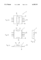
- FIGS. 1a to 1d are a bottom view, a plan, a front view and a side elevation, respectively, of a semiconductor device of a first embodiment according to the present invention.
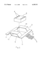
- FIG. 2 is an exploded perspective view showing a form and the positional relationship of a radiation plate, a lead terminal and a pellet of the semiconductor device shown in FIGS. 1a to 1d.
- FIG. 3 is a front view showing an internal structure of the semiconductor device shown in FIGS. 1a to 1d.
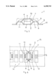
- FIG. 4 is a plan showing a lead frame in one process of a manufacturing method according to the semiconductor device shown in FIGS. 1a to 1d.
- FIGS. 5a to 5d are a bottom view, a plan, a front view and a side elevation, respectively, of a modified example of the semiconductor device of the first embodiment according to the present invention.
- FIG. 6 is a plan illustrating a lead frame in one process of a manufacturing method of the semiconductor device shown in FIGS. 5a to 5d.
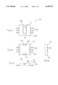
- FIG. 7 is a front view showing an internal structure of a semiconductor device of a second embodiment according to the present invention.
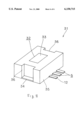
- FIG. 8 is a perspective view showing an external appearance of the semiconductor device shown in FIG. 7.
- a semiconductor device 1 As shown in FIGS. 1a to 1d, FIG. 2 and FIG. 3, a semiconductor device 1 according to the present embodiment has a semiconductor pellet 2 on which an integrated circuit is formed.
- the pellet 2 is placed on a radiation plate 3 which serves as a metal die pad.
- a plurality of electrode pads 4 are provided on the surface of the pellet 2, and a plurality of lead terminals 5 are arrayed on both sides of the radiation plate 3.
- the electrode pads 4 and the inner portions 6 of the lead terminals 5 are connected by bonding wires 7 respectively, and the pellet 2, a part of the radiation plate 3, the bonding wires 7, the inner portions 6 of the lead terminals 5 are encapsulated in the resin member 8 of a flat rectangular parallelepiped shape.
- the radiation plate 3 is formed in a shape in which both end portions 10 at the opposite ends of the central portion 9 are positioned higher than the central portion 9.
- the pellet 2 is placed on the upper surface of the central portion 9.
- the upper surface of both the end portions 10 of the radiation plate 3 are exposed to the outside from the upper surface of the resin member 8 and the under surface of the central portion 9 of the radiation plate 3 is exposed to the outside from lower surface of the resin member 8.
- the central portion 9 of the radiation plate 3 is formed on the whole in a downwardly projected concave shape with both right and left sides bent upwards, and both the end portions 10 are each formed on the whole in an upwardly projected convex shape with both right and left sides bent downwards.
- Both side portions 11 of the radiation plate 3 are formed in a longitudinally slender rectangular shape. The side portions 11 are connected with the central portion 9 and the end portions 10.
- the lead terminals 5 are formed in a crank shape and outer portions 12 projected from the resin member 8 are situated on a surface of the same level with the lower surface of the resin member 8. Inner portions 6 of the lead terminals 5 are positioned higher than the outer portions 12, for example, positioned on a surface of the same level with the upper surface of the pellet 2 and the upper surface of both the side portions 11 of the radiation plate 3.
- the semiconductor device 1 is mounted on a upper surface of a circuit substrate (not shown).
- the outer portions 12 of a plurality of lead terminals 5 projected from the side of the resin member 8 are connected with a plurality of signal lines of the circuit substrate respectively by means of solder, and the under surface of the central portion 9 of the radiation plate 3 exposed to the outside from the under surface of the resin member 8 is connected with a conductor pattern such as ground wiring of the circuit substrate by means of solder.
- the semiconductor device 1 can execute processing of various signals.
- the pellet 2 which functions in this way generates heat inevitably, but the generated heat is well radiated through the radiation plate 3.
- the central portion 9 of the radiation plate 3 on which the pellet 2 is mounted is exposed to the outside from the lower surface of the resin member 8, the central portion 9 being directly connected with the conductor pattern of the circuit substrate, and hence the heat generated in the pellet 2 can suitably be radiated to the circuit substrate through the central portion 9.
- the heat generated in the pellet 2 can preferably be radiated to the ambient open air by the radiation plate 3 through both the end portions 10 thereof.
- the semiconductor device 1 of the present embodiment can radiate the heat generated in the pellet 2 to both the conductor pattern of the circuit substrate and the ambient open air through the radiation plate 3. Therefore, for example, even if the temperature of either one of the circuit substrate or the open air is high, when the temperature of the other one is low, it is possible to satisfactorily radiate the heat generated in the pellet 2.
- the central portion 9 and both the end portions 10 of a piece of radiation plate 3 are positioned on the lower and upper surfaces of the resin member 8, respectively, it is unnecessary to provide the radiation plate 3 with an exclusive use holder to be positioned inside the resin member 8, because the radiation plate 3 being prevented from falling off the resin member 8.
- a manufacturing method of the semiconductor device 1 of the present embodiment will be described below with brief with reference to FIG. 4 and the like.
- unit pattern 14 in which a plurality of lead terminals 5 and a piece of radiation plate 3 are unitedly coupled by tiebars 13, is formed in a lead frame 15. It is noted that, in FIG. 4, only two pieces of unit patterns 14 of the semiconductor device 1 are formed in the lead frame 15 for simplifying the description, but in the real manufacture a number of unit patterns 14 are successively formed in a piece of lead frame 15.
- the central portion 9 and both the end portions 10 of the radiation plate 3 are separated by a pair of laterally slender slit-shaped penetration holes, by deforming the lead frame 15 by means of a lead forming die, the central portion 9 of the radiation plate 3 is bent into a downwardly projected concave form and both the end portions 10 are each bent into an upwardly projected convex form and concurrently the lead terminals 5 are bent into a crank form making the inner portions 6 position higher than the outer portions 12.
- the pellet 2 is placed on the upper surface of the central portion 9 of the radiation plate 3, then the electrode pads 4 on the upper surface of the pellet 2 and the inner portions 6 of the lead terminals 5 are connected with the bonding wires 7 respectively.
- both the end portions 10 of the radiation plate 3 are positioned higher than the upper surface of the pellet 2 but are not positioned over the pellet 2, and hence the connection with the bonding wires 7 is easily executed.
- the lead frame 15 in which the pellet 2 and the bonding wires 7 are mounted in a unit in this way is disposed inside a cavity of a pair of detachable molds. At this time, by holding the outer portions 12 of the lead terminals 5 with a pair of molds and at the same time making the lower surface of the central portion 9 and the upper surface of both the end portions 10 of the radiation plate 3 contact the inner surface of the mold, these portions are arranged exposed to the outside from the resin member 8.
- the resin member 8 By filling melted resin in the cavity of the mold and making it solidify in the above described state, the resin member 8 is formed including the pellet 2, a part of the radiation plate 3, the bonding wires 7 and the inner portions 6 of the lead terminals 5, all encapsulated in the resin member 8. Subsequently, by taking out this resin member 8 from the mold, removing such as flashes of resin and cutting off the tiebars 13 of the lead frame 15, the semiconductor device 1 is completed as shown in FIG. 1.
- the structure of the semiconductor device 1, in which the lower surface of the central portion 9 of the radiation plate 3 is exposed to the outside from the lower surface of the resin member 8 and the upper surface of both the end portions 10 of the radiation plate 3 are exposed to the outside from both ends of the upper surface of the resin member 8, can be realized simply. Further, since the radiation plate 3 and the lead terminals 5 are concurrently formed from one piece of the lead frame 15, the productivity is better when compared to the case in which the radiation plate 3 and the lead terminals 5 are formed separately.
- the present invention is not limited to the above structure, but various modifications can be made within the scope of not deviating from the gist of the present invention.
- the above structure of the present invention there is shown an example in which both the end portions 10 of the radiation plate 3 exposed to the outside from both ends of the upper surface of the resin member 8 radiate heat by directly contacting the open air, however, for example, it is possible to increase the heat radiation effect by mounting a heat sink (not shown) on each of both the end portions 10 of the radiation plate 3. Further, it is possible to adhere the upper surface of both the end portions 10 of the radiation plate 3 to the lower surface of a large-sized radiation plate (not shown) larger than the resin member 8 and fix both end portions of this large radiation plate to the circuit substrate with screws.
- both the end portions 10 of the radiation plate 3 are designed so that they do not protrude outside from the end surface of the resin member 8 to form the whole body in a reduced size, it is possible to protrude both the end portions 10 of the radiation plate 3 from the end surface of the resin member 8 to increase the heat radiation effect.
- both the end portions 10 of the radiation plate 3 are exposed to the outside from the front and rear surfaces on both ends of the upper surface of the resin member 8, however, as shown in FIGS. 5a to 5d, it is possible to provide a semiconductor device 21 which both end portions 23 of a radiation plate 22 are positioned on both ends of the upper surface of a resin member 24 slightly inside from the front and the rear edges, respectively.
- a semiconductor device 21 which both end portions 23 of a radiation plate 22 are positioned on both ends of the upper surface of a resin member 24 slightly inside from the front and the rear edges, respectively.
- tiebars 26 which support the radiation plate 22 of the lead frame 25 with the resin member 24 and cut off the tiebars 26 projected from the resin member 24.
- FIG. 7 and FIG. 8 A second embodiment of the present invention will be described below with reference to FIG. 7 and FIG. 8. With reference to the part of the second embodiment which is the same as that of the above first embodiment, the same symbol as that of the first embodiment will be used while omitting the detailed description thereof.
- a semiconductor pellet 2 on which an integrated circuit is formed is mounted on a radiation plate 32 which serves as a metal die pad, a plurality of electrode pads 4 of the pellet 2 are connected with a plurality of lead terminals 5 arrayed on both sides of the radiation plate 32 by means of bonding wires 7, respectively.
- the radiation plate 32 is formed in a shape in which a central portion 33 is positioned higher than both end portions 34, the pellet 2 being placed on the lower surface of the central portion 33.
- the upper surface of the central portion 33 of the radiation plate 32 is exposed to the outside from the upper surface of the resin member 35, and the under surfaces of both the end portions 34 of the radiation plate 32 are exposed to the outside from both ends of the lower surface of the resin member 35.
- the radiation plate 32 of the semiconductor device 31 of the present embodiment is formed in a shape obtained by disposing the radiation plate 3 of the foregoing semiconductor device 1 upside down. It is noted that concave portions 36 are provided in the front and rear ends of the resin member 35 running from the upper surface to the lower surface thereof, respectively, both the end portions 34 of the radiation plate 32 being disposed in bottoms of these concave portions 36.
- the semiconductor device 31 of the present embodiment is mounted on the upper surface of a circuit substrate (not shown) in the same way as the foregoing semiconductor device 1.
- the outer portions 12 of a plurality of lead terminals 5 projected from the side of the resin member 35 are individually connected with a plurality of signal lines of the circuit substrate by means of solder, and the lower surface of both the end portions 34 of the radiation plate 32 exposed to the outside from both ends of the lower surface of the resin member 35 are connected with a conductor pattern such as ground wiring of the circuit substrate by means of solder.
- both the end portions 34 of the radiation plate 32 on which the pellet 2 is placed are exposed to the outside from the lower surface of the resin member 35, both the end portions 34 being directly connected with the conductor pattern of the circuit substrate by means of solder, and hence the heat generated in the pellet 2 can suitably be radiated to the circuit substrate by the radiation plate 32 through both the end portions 34 thereof.
- the heat generated in the pellet 2 can preferably be radiated also to the ambient open air by the radiation plate 32 through the central portion 33 thereof.
- the semiconductor device 31 of the present embodiment can radiate the heat generated in the pellet 2 to both the conductor pattern of the circuit substrate and the ambient open air through the radiation plate 32. Therefore, for example, even if the temperature of either one of the circuit substrate or the open air is high, when the temperature of the other one is low, it is possible to satisfactorily radiate the heat generated in the pellet 2.
- the pellet 2 is placed upside down on the lower surface of the central portion 33 of the radiation plate 32, but since the bonding wires 7 connect the electrode pads 4 of the pellet 2 and the lower surface of the inner portions 6 of the lead terminals 5, this connection can easily be performed.
- the bonding wires 7 are not to be exposed outside from the resin member 35. Since both the end portions 34 of the radiation plate 32 are situated lower than the under surface of the pellet 2 but not right beneath thereof, connection by the bonding wires 7 is easy.
- both the end portions 34 of the radiation plate 32 are exposed to the outside from the under portion of the resin member 35, respectively, it is easy to connect both the end portions 34 of the radiation plate 32 to the conductor pattern of the circuit substrate by means of solder.
- both the end portions 34 of the radiation plate 32 are positioned in bottoms of the concave portions 36 of the resin member 35 each exposing the upper and the end surfaces to the outside, it can easily be connected in a large area to the conductor pattern of the circuit substrate by means of solder or the like.
- the lead frame 15 having a plurality of the lead terminals 5 and a piece of radiation plate 32 unitedly coupled by means of tiebars 13 is formed.
- the central portion 33 and both the end portions 34 of the radiation plate 32 are separated by a pair of laterally slender slit-shaped penetration holes by the above etching process, by deforming the lead frame 15 by means of a lead forming die, the central portion 33 of the radiation plate 32 is bent into an upwardly projected convex form and both the end portions 34 are each bent into a downwardly projected concave form and concurrently the lead terminals 5 are bent into a crank form making inner portions 6 position higher than outer portions 12.
- the lead frame 15 in which the pellet 2 and the bonding wires 7 are placed in a unit in this way is disposed inside a cavity of a pair of detachable molds. At this time, by holding the outer portions 12 of the lead terminals 5 and both the end portions 34 of the radiation plate 32 with a pair of molds and at the same time making the upper surface of the central portion 33 of the radiation plate 32 contact the inner surface of the mold, these portions are arranged to be exposed outside from the resin member 35.
- the resin member 35 is formed including the pellet 2, a part of radiation plate 32, the bonding wires 7 and the inner parts 6 of the lead terminals 5, all encapsulated in the resin member 35. Subsequently, by taking out this resin member 35 from the mold, removing such as flashes of resin and cutting off the tiebars 13 of the lead frame 15, the semiconductor device 31 is completed as shown in FIG. 8.
- the structure of the semiconductor device 31 in which the upper surface of the central portion 33 of the radiation plate 32 is exposed to the outside from upper surface of the resin member 35 and the lower surfaces of both the end portions 34 of the radiation plate 32 are exposed to the outside from both ends of the lower surface of the resin member 35, can simply be realized.
Abstract
Description
Claims (6)
Applications Claiming Priority (2)
| Application Number | Priority Date | Filing Date | Title |
|---|---|---|---|
| JP9210849A JP3003638B2 (en) | 1997-08-05 | 1997-08-05 | Semiconductor device and manufacturing method thereof |
| JP9-210849 | 1997-08-05 |
Publications (1)
| Publication Number | Publication Date |
|---|---|
| US6150715A true US6150715A (en) | 2000-11-21 |
Family
ID=16596134
Family Applications (1)
| Application Number | Title | Priority Date | Filing Date |
|---|---|---|---|
| US09/123,448 Expired - Lifetime US6150715A (en) | 1997-08-05 | 1998-07-28 | Semiconductor device with radiation plate for high radiation character and method of manufacturing the same |
Country Status (3)
| Country | Link |
|---|---|
| US (1) | US6150715A (en) |
| JP (1) | JP3003638B2 (en) |
| CN (1) | CN1130767C (en) |
Cited By (6)
| Publication number | Priority date | Publication date | Assignee | Title |
|---|---|---|---|---|
| US6307255B1 (en) * | 1994-11-10 | 2001-10-23 | Micron Technology, Inc. | Multi-layer lead frame for a semiconductor device |
| US20040113240A1 (en) * | 2002-10-11 | 2004-06-17 | Wolfgang Hauser | An electronic component with a leadframe |
| WO2005038915A1 (en) * | 2003-10-17 | 2005-04-28 | Koninklijke Philips Electronics, N.V. | Method for providing double-sided cooling of leadframe-based wire-bonded electronic packages and device produced thereby |
| US20100001385A1 (en) * | 2008-07-07 | 2010-01-07 | Jose Alvin Caparas | Integrated circuit package system with bumped lead and nonbumped lead |
| US20110124158A1 (en) * | 2005-12-09 | 2011-05-26 | Fairchild Semiconductor Corporation | Thermal enhanced upper and dual heat sink exposed molded leadless package |
| US20160037690A1 (en) * | 2014-07-29 | 2016-02-04 | Toyota Jidosha Kabushiki Kaisha | Electromagnetic shield body and box |
Families Citing this family (3)
| Publication number | Priority date | Publication date | Assignee | Title |
|---|---|---|---|---|
| US8304887B2 (en) * | 2009-12-10 | 2012-11-06 | Texas Instruments Incorporated | Module package with embedded substrate and leadframe |
| JP6046063B2 (en) * | 2014-01-22 | 2016-12-14 | 古河電気工業株式会社 | substrate |
| JP2015149363A (en) * | 2014-02-05 | 2015-08-20 | 株式会社デンソー | semiconductor module |
Citations (16)
| Publication number | Priority date | Publication date | Assignee | Title |
|---|---|---|---|---|
| US3820153A (en) * | 1972-08-28 | 1974-06-25 | Zyrotron Ind Inc | Plurality of semiconductor elements mounted on common base |
| US3825803A (en) * | 1972-04-06 | 1974-07-23 | Philips Corp | Semiconductor lead and heat sink structure |
| US4392151A (en) * | 1979-08-29 | 1983-07-05 | Mitsubishi Denki Kabushiki Kaisha | Semiconductor device |
| US4465130A (en) * | 1982-07-06 | 1984-08-14 | Burroughs Corporation | Wire form heat exchange element |
| JPH06252318A (en) * | 1993-02-26 | 1994-09-09 | Fujitsu Ltd | Semiconductor device and manufacture thereof |
| US5365106A (en) * | 1992-10-27 | 1994-11-15 | Kabushiki Kaisha Toshiba | Resin mold semiconductor device |
| US5434407A (en) * | 1993-08-23 | 1995-07-18 | Gentex Corporation | Automatic rearview mirror incorporating light pipe |
| US5479050A (en) * | 1990-10-18 | 1995-12-26 | Texas Instruments Incorporated | Leadframe with pedestal |
| JPH08111491A (en) * | 1994-10-12 | 1996-04-30 | Toshiba Corp | Semiconductor device |
| US5629561A (en) * | 1994-12-16 | 1997-05-13 | Anam Industrial Co., Ltd. | Semiconductor package with integral heat dissipator |
| US5637923A (en) * | 1991-10-17 | 1997-06-10 | Fujitsu Limited | Semiconductor device, carrier for carrying semiconductor device |
| US5703398A (en) * | 1993-03-17 | 1997-12-30 | Fujitsu Limited | Semiconductor integrated circuit device and method of producing the semiconductor integrated circuit device |
| US5789812A (en) * | 1993-10-15 | 1998-08-04 | Nec Corporation | Semiconductor package |
| US5859387A (en) * | 1996-11-29 | 1999-01-12 | Allegro Microsystems, Inc. | Semiconductor device leadframe die attach pad having a raised bond pad |
| US5869889A (en) * | 1997-04-21 | 1999-02-09 | Lsi Logic Corporation | Thin power tape ball grid array package |
| JP2907186B2 (en) * | 1997-05-19 | 1999-06-21 | 日本電気株式会社 | Semiconductor device and manufacturing method thereof |
-
1997
- 1997-08-05 JP JP9210849A patent/JP3003638B2/en not_active Expired - Fee Related
-
1998
- 1998-07-28 US US09/123,448 patent/US6150715A/en not_active Expired - Lifetime
- 1998-08-05 CN CN98117858A patent/CN1130767C/en not_active Expired - Fee Related
Patent Citations (17)
| Publication number | Priority date | Publication date | Assignee | Title |
|---|---|---|---|---|
| US3825803A (en) * | 1972-04-06 | 1974-07-23 | Philips Corp | Semiconductor lead and heat sink structure |
| US3820153A (en) * | 1972-08-28 | 1974-06-25 | Zyrotron Ind Inc | Plurality of semiconductor elements mounted on common base |
| US4392151A (en) * | 1979-08-29 | 1983-07-05 | Mitsubishi Denki Kabushiki Kaisha | Semiconductor device |
| US4465130A (en) * | 1982-07-06 | 1984-08-14 | Burroughs Corporation | Wire form heat exchange element |
| US5479050A (en) * | 1990-10-18 | 1995-12-26 | Texas Instruments Incorporated | Leadframe with pedestal |
| US5637923A (en) * | 1991-10-17 | 1997-06-10 | Fujitsu Limited | Semiconductor device, carrier for carrying semiconductor device |
| US5365106A (en) * | 1992-10-27 | 1994-11-15 | Kabushiki Kaisha Toshiba | Resin mold semiconductor device |
| JPH06252318A (en) * | 1993-02-26 | 1994-09-09 | Fujitsu Ltd | Semiconductor device and manufacture thereof |
| US5703398A (en) * | 1993-03-17 | 1997-12-30 | Fujitsu Limited | Semiconductor integrated circuit device and method of producing the semiconductor integrated circuit device |
| US5434407A (en) * | 1993-08-23 | 1995-07-18 | Gentex Corporation | Automatic rearview mirror incorporating light pipe |
| US5789812A (en) * | 1993-10-15 | 1998-08-04 | Nec Corporation | Semiconductor package |
| US5583371A (en) * | 1994-10-12 | 1996-12-10 | Kabushiki Kaisha Toshiba | Resin-sealed semiconductor device capable of improving in heat radiation characteristics of resin-sealed semiconductor elements |
| JPH08111491A (en) * | 1994-10-12 | 1996-04-30 | Toshiba Corp | Semiconductor device |
| US5629561A (en) * | 1994-12-16 | 1997-05-13 | Anam Industrial Co., Ltd. | Semiconductor package with integral heat dissipator |
| US5859387A (en) * | 1996-11-29 | 1999-01-12 | Allegro Microsystems, Inc. | Semiconductor device leadframe die attach pad having a raised bond pad |
| US5869889A (en) * | 1997-04-21 | 1999-02-09 | Lsi Logic Corporation | Thin power tape ball grid array package |
| JP2907186B2 (en) * | 1997-05-19 | 1999-06-21 | 日本電気株式会社 | Semiconductor device and manufacturing method thereof |
Cited By (13)
| Publication number | Priority date | Publication date | Assignee | Title |
|---|---|---|---|---|
| US6307255B1 (en) * | 1994-11-10 | 2001-10-23 | Micron Technology, Inc. | Multi-layer lead frame for a semiconductor device |
| US6515353B2 (en) | 1996-09-04 | 2003-02-04 | Micron Technology, Inc. | Multi-layer lead frame for a semiconductor device |
| US6707136B2 (en) | 1996-09-04 | 2004-03-16 | Micron Technology, Inc. | Multi-layer lead frame for a semiconductor device |
| US9620391B2 (en) | 2002-10-11 | 2017-04-11 | Micronas Gmbh | Electronic component with a leadframe |
| US20040113240A1 (en) * | 2002-10-11 | 2004-06-17 | Wolfgang Hauser | An electronic component with a leadframe |
| WO2005038915A1 (en) * | 2003-10-17 | 2005-04-28 | Koninklijke Philips Electronics, N.V. | Method for providing double-sided cooling of leadframe-based wire-bonded electronic packages and device produced thereby |
| US20070085173A1 (en) * | 2003-10-17 | 2007-04-19 | Koninklijke Philips Electronics N.V. | Method and apparatus for providing double-sided cooling of leadframe-based wire-bonded electronic packages |
| US20110124158A1 (en) * | 2005-12-09 | 2011-05-26 | Fairchild Semiconductor Corporation | Thermal enhanced upper and dual heat sink exposed molded leadless package |
| US8278742B2 (en) * | 2005-12-09 | 2012-10-02 | Fairchild Semiconductor Corporation | Thermal enhanced upper and dual heat sink exposed molded leadless package and method |
| US20100001385A1 (en) * | 2008-07-07 | 2010-01-07 | Jose Alvin Caparas | Integrated circuit package system with bumped lead and nonbumped lead |
| US8455988B2 (en) * | 2008-07-07 | 2013-06-04 | Stats Chippac Ltd. | Integrated circuit package system with bumped lead and nonbumped lead |
| US20160037690A1 (en) * | 2014-07-29 | 2016-02-04 | Toyota Jidosha Kabushiki Kaisha | Electromagnetic shield body and box |
| CN105324021A (en) * | 2014-07-29 | 2016-02-10 | 丰田自动车株式会社 | Electromagnetic shield body and box |
Also Published As
| Publication number | Publication date |
|---|---|
| JPH1154683A (en) | 1999-02-26 |
| CN1211072A (en) | 1999-03-17 |
| CN1130767C (en) | 2003-12-10 |
| JP3003638B2 (en) | 2000-01-31 |
Similar Documents
| Publication | Publication Date | Title |
|---|---|---|
| US6319753B1 (en) | Semiconductor device having lead terminals bent in J-shape | |
| JP4729244B2 (en) | Non-mold package for semiconductor devices | |
| EP0880176B1 (en) | Semiconductor device having pellet mounted on radiating plate thereof | |
| US6552428B1 (en) | Semiconductor package having an exposed heat spreader | |
| US6813154B2 (en) | Reversible heat sink packaging assembly for an integrated circuit | |
| US6979594B1 (en) | Process for manufacturing ball grid array package | |
| US6987032B1 (en) | Ball grid array package and process for manufacturing same | |
| JP2001313363A (en) | Resin-encapsulated semiconductor device | |
| US20080233679A1 (en) | Semiconductor package with plated connection | |
| US6150715A (en) | Semiconductor device with radiation plate for high radiation character and method of manufacturing the same | |
| US5249354A (en) | Method of making electronic component packages | |
| US6255135B1 (en) | Quad flat pack integrated circuit package | |
| JPH11214596A (en) | Semiconductor device and its manufacturing method and electronic apparatus | |
| JP3061120B2 (en) | Semiconductor device and manufacturing method thereof | |
| JPH0661372A (en) | Hybrid ic | |
| JPH03108745A (en) | Semiconductor device | |
| JPH03214763A (en) | Lead frame for semiconductor integrated circuit device and the device using the same | |
| KR100342812B1 (en) | Area array bumped semiconductor package having ground and power lines | |
| KR100342811B1 (en) | Area array bumped semiconductor package with chips | |
| JP2976941B2 (en) | Semiconductor device and manufacturing method thereof | |
| KR0147157B1 (en) | "t" type high integrated semiconductor package | |
| JPS6365660A (en) | Semiconductor integrated circuit device | |
| JPH06104356A (en) | Surface mounting semiconductor device | |
| JPH06342873A (en) | Manufacture of semiconductor device | |
| KR19980039679A (en) | Lead-on Chip Area Array Bumped Semiconductor Package |
Legal Events
| Date | Code | Title | Description |
|---|---|---|---|
| AS | Assignment |
Owner name: NEC CORPORATION, JAPAN Free format text: ASSIGNMENT OF ASSIGNORS INTEREST;ASSIGNORS:ICHIKAWA, SEIJI;UMEMOTO, TAKESHI;SATO, KAZUNARI;AND OTHERS;REEL/FRAME:009356/0001 Effective date: 19980722 |
|
| STCF | Information on status: patent grant |
Free format text: PATENTED CASE |
|
| FEPP | Fee payment procedure |
Free format text: PAYOR NUMBER ASSIGNED (ORIGINAL EVENT CODE: ASPN); ENTITY STATUS OF PATENT OWNER: LARGE ENTITY |
|
| AS | Assignment |
Owner name: NEC COMPOUND SEMICONDUCTOR DEVICES, LTD., JAPAN Free format text: ASSIGNMENT OF ASSIGNORS INTEREST;ASSIGNOR:NEC CORPORATION;REEL/FRAME:013352/0935 Effective date: 20020919 |
|
| FPAY | Fee payment |
Year of fee payment: 4 |
|
| AS | Assignment |
Owner name: NEC ELECTRONICS CORPORATION, JAPAN Free format text: ASSIGNMENT OF ASSIGNORS INTEREST;ASSIGNOR:NEC COMPOUND SEMICONDUCTOR DEVICES, LTD.;REEL/FRAME:017422/0528 Effective date: 20060315 |
|
| FPAY | Fee payment |
Year of fee payment: 8 |
|
| AS | Assignment |
Owner name: RENESAS ELECTRONICS CORPORATION, JAPAN Free format text: CHANGE OF NAME;ASSIGNOR:NEC ELECTRONICS CORPORATION;REEL/FRAME:025183/0574 Effective date: 20100401 |
|
| FPAY | Fee payment |
Year of fee payment: 12 |
|
| AS | Assignment |
Owner name: RENESAS ELECTRONICS CORPORATION, JAPAN Free format text: CHANGE OF ADDRESS;ASSIGNOR:RENESAS ELECTRONICS CORPORATION;REEL/FRAME:044928/0001 Effective date: 20150806 |