US6148509A - Method for supporting an integrated circuit die - Google Patents
Method for supporting an integrated circuit die Download PDFInfo
- Publication number
- US6148509A US6148509A US09/141,004 US14100498A US6148509A US 6148509 A US6148509 A US 6148509A US 14100498 A US14100498 A US 14100498A US 6148509 A US6148509 A US 6148509A
- Authority
- US
- United States
- Prior art keywords
- integrated circuit
- die
- circuit die
- edge
- package
- Prior art date
- Legal status (The legal status is an assumption and is not a legal conclusion. Google has not performed a legal analysis and makes no representation as to the accuracy of the status listed.)
- Expired - Lifetime
Links
Images


Classifications
-
- H—ELECTRICITY
- H01—ELECTRIC ELEMENTS
- H01L—SEMICONDUCTOR DEVICES NOT COVERED BY CLASS H10
- H01L23/00—Details of semiconductor or other solid state devices
- H01L23/48—Arrangements for conducting electric current to or from the solid state body in operation, e.g. leads, terminal arrangements ; Selection of materials therefor
- H01L23/488—Arrangements for conducting electric current to or from the solid state body in operation, e.g. leads, terminal arrangements ; Selection of materials therefor consisting of soldered or bonded constructions
- H01L23/495—Lead-frames or other flat leads
- H01L23/49541—Geometry of the lead-frame
-
- H—ELECTRICITY
- H01—ELECTRIC ELEMENTS
- H01L—SEMICONDUCTOR DEVICES NOT COVERED BY CLASS H10
- H01L23/00—Details of semiconductor or other solid state devices
- H01L23/48—Arrangements for conducting electric current to or from the solid state body in operation, e.g. leads, terminal arrangements ; Selection of materials therefor
- H01L23/488—Arrangements for conducting electric current to or from the solid state body in operation, e.g. leads, terminal arrangements ; Selection of materials therefor consisting of soldered or bonded constructions
- H01L23/495—Lead-frames or other flat leads
- H01L23/49503—Lead-frames or other flat leads characterised by the die pad
- H01L23/4951—Chip-on-leads or leads-on-chip techniques, i.e. inner lead fingers being used as die pad
-
- H—ELECTRICITY
- H01—ELECTRIC ELEMENTS
- H01L—SEMICONDUCTOR DEVICES NOT COVERED BY CLASS H10
- H01L23/00—Details of semiconductor or other solid state devices
- H01L23/48—Arrangements for conducting electric current to or from the solid state body in operation, e.g. leads, terminal arrangements ; Selection of materials therefor
- H01L23/488—Arrangements for conducting electric current to or from the solid state body in operation, e.g. leads, terminal arrangements ; Selection of materials therefor consisting of soldered or bonded constructions
- H01L23/495—Lead-frames or other flat leads
- H01L23/49568—Lead-frames or other flat leads specifically adapted to facilitate heat dissipation
-
- H—ELECTRICITY
- H01—ELECTRIC ELEMENTS
- H01L—SEMICONDUCTOR DEVICES NOT COVERED BY CLASS H10
- H01L2224/00—Indexing scheme for arrangements for connecting or disconnecting semiconductor or solid-state bodies and methods related thereto as covered by H01L24/00
- H01L2224/01—Means for bonding being attached to, or being formed on, the surface to be connected, e.g. chip-to-package, die-attach, "first-level" interconnects; Manufacturing methods related thereto
- H01L2224/42—Wire connectors; Manufacturing methods related thereto
- H01L2224/47—Structure, shape, material or disposition of the wire connectors after the connecting process
- H01L2224/48—Structure, shape, material or disposition of the wire connectors after the connecting process of an individual wire connector
- H01L2224/4805—Shape
- H01L2224/4809—Loop shape
- H01L2224/48091—Arched
-
- H—ELECTRICITY
- H01—ELECTRIC ELEMENTS
- H01L—SEMICONDUCTOR DEVICES NOT COVERED BY CLASS H10
- H01L2224/00—Indexing scheme for arrangements for connecting or disconnecting semiconductor or solid-state bodies and methods related thereto as covered by H01L24/00
- H01L2224/01—Means for bonding being attached to, or being formed on, the surface to be connected, e.g. chip-to-package, die-attach, "first-level" interconnects; Manufacturing methods related thereto
- H01L2224/42—Wire connectors; Manufacturing methods related thereto
- H01L2224/47—Structure, shape, material or disposition of the wire connectors after the connecting process
- H01L2224/48—Structure, shape, material or disposition of the wire connectors after the connecting process of an individual wire connector
- H01L2224/481—Disposition
- H01L2224/48151—Connecting between a semiconductor or solid-state body and an item not being a semiconductor or solid-state body, e.g. chip-to-substrate, chip-to-passive
- H01L2224/48221—Connecting between a semiconductor or solid-state body and an item not being a semiconductor or solid-state body, e.g. chip-to-substrate, chip-to-passive the body and the item being stacked
- H01L2224/48245—Connecting between a semiconductor or solid-state body and an item not being a semiconductor or solid-state body, e.g. chip-to-substrate, chip-to-passive the body and the item being stacked the item being metallic
- H01L2224/48247—Connecting between a semiconductor or solid-state body and an item not being a semiconductor or solid-state body, e.g. chip-to-substrate, chip-to-passive the body and the item being stacked the item being metallic connecting the wire to a bond pad of the item
-
- H—ELECTRICITY
- H01—ELECTRIC ELEMENTS
- H01L—SEMICONDUCTOR DEVICES NOT COVERED BY CLASS H10
- H01L2224/00—Indexing scheme for arrangements for connecting or disconnecting semiconductor or solid-state bodies and methods related thereto as covered by H01L24/00
- H01L2224/01—Means for bonding being attached to, or being formed on, the surface to be connected, e.g. chip-to-package, die-attach, "first-level" interconnects; Manufacturing methods related thereto
- H01L2224/42—Wire connectors; Manufacturing methods related thereto
- H01L2224/47—Structure, shape, material or disposition of the wire connectors after the connecting process
- H01L2224/48—Structure, shape, material or disposition of the wire connectors after the connecting process of an individual wire connector
- H01L2224/481—Disposition
- H01L2224/48151—Connecting between a semiconductor or solid-state body and an item not being a semiconductor or solid-state body, e.g. chip-to-substrate, chip-to-passive
- H01L2224/48221—Connecting between a semiconductor or solid-state body and an item not being a semiconductor or solid-state body, e.g. chip-to-substrate, chip-to-passive the body and the item being stacked
- H01L2224/48245—Connecting between a semiconductor or solid-state body and an item not being a semiconductor or solid-state body, e.g. chip-to-substrate, chip-to-passive the body and the item being stacked the item being metallic
- H01L2224/4826—Connecting between the body and an opposite side of the item with respect to the body
-
- H—ELECTRICITY
- H01—ELECTRIC ELEMENTS
- H01L—SEMICONDUCTOR DEVICES NOT COVERED BY CLASS H10
- H01L2224/00—Indexing scheme for arrangements for connecting or disconnecting semiconductor or solid-state bodies and methods related thereto as covered by H01L24/00
- H01L2224/73—Means for bonding being of different types provided for in two or more of groups H01L2224/10, H01L2224/18, H01L2224/26, H01L2224/34, H01L2224/42, H01L2224/50, H01L2224/63, H01L2224/71
- H01L2224/732—Location after the connecting process
- H01L2224/73201—Location after the connecting process on the same surface
- H01L2224/73215—Layer and wire connectors
-
- H—ELECTRICITY
- H01—ELECTRIC ELEMENTS
- H01L—SEMICONDUCTOR DEVICES NOT COVERED BY CLASS H10
- H01L24/00—Arrangements for connecting or disconnecting semiconductor or solid-state bodies; Methods or apparatus related thereto
- H01L24/01—Means for bonding being attached to, or being formed on, the surface to be connected, e.g. chip-to-package, die-attach, "first-level" interconnects; Manufacturing methods related thereto
- H01L24/42—Wire connectors; Manufacturing methods related thereto
- H01L24/47—Structure, shape, material or disposition of the wire connectors after the connecting process
- H01L24/48—Structure, shape, material or disposition of the wire connectors after the connecting process of an individual wire connector
-
- H—ELECTRICITY
- H01—ELECTRIC ELEMENTS
- H01L—SEMICONDUCTOR DEVICES NOT COVERED BY CLASS H10
- H01L2924/00—Indexing scheme for arrangements or methods for connecting or disconnecting semiconductor or solid-state bodies as covered by H01L24/00
- H01L2924/0001—Technical content checked by a classifier
- H01L2924/00014—Technical content checked by a classifier the subject-matter covered by the group, the symbol of which is combined with the symbol of this group, being disclosed without further technical details
-
- H—ELECTRICITY
- H01—ELECTRIC ELEMENTS
- H01L—SEMICONDUCTOR DEVICES NOT COVERED BY CLASS H10
- H01L2924/00—Indexing scheme for arrangements or methods for connecting or disconnecting semiconductor or solid-state bodies as covered by H01L24/00
- H01L2924/06—Polymers
- H01L2924/078—Adhesive characteristics other than chemical
- H01L2924/07802—Adhesive characteristics other than chemical not being an ohmic electrical conductor
-
- H—ELECTRICITY
- H01—ELECTRIC ELEMENTS
- H01L—SEMICONDUCTOR DEVICES NOT COVERED BY CLASS H10
- H01L2924/00—Indexing scheme for arrangements or methods for connecting or disconnecting semiconductor or solid-state bodies as covered by H01L24/00
- H01L2924/10—Details of semiconductor or other solid state devices to be connected
- H01L2924/102—Material of the semiconductor or solid state bodies
- H01L2924/1025—Semiconducting materials
- H01L2924/10251—Elemental semiconductors, i.e. Group IV
- H01L2924/10253—Silicon [Si]
-
- H—ELECTRICITY
- H01—ELECTRIC ELEMENTS
- H01L—SEMICONDUCTOR DEVICES NOT COVERED BY CLASS H10
- H01L2924/00—Indexing scheme for arrangements or methods for connecting or disconnecting semiconductor or solid-state bodies as covered by H01L24/00
- H01L2924/10—Details of semiconductor or other solid state devices to be connected
- H01L2924/11—Device type
- H01L2924/14—Integrated circuits
-
- Y—GENERAL TAGGING OF NEW TECHNOLOGICAL DEVELOPMENTS; GENERAL TAGGING OF CROSS-SECTIONAL TECHNOLOGIES SPANNING OVER SEVERAL SECTIONS OF THE IPC; TECHNICAL SUBJECTS COVERED BY FORMER USPC CROSS-REFERENCE ART COLLECTIONS [XRACs] AND DIGESTS
- Y10—TECHNICAL SUBJECTS COVERED BY FORMER USPC
- Y10T—TECHNICAL SUBJECTS COVERED BY FORMER US CLASSIFICATION
- Y10T29/00—Metal working
- Y10T29/49—Method of mechanical manufacture
- Y10T29/49002—Electrical device making
- Y10T29/49117—Conductor or circuit manufacturing
- Y10T29/49121—Beam lead frame or beam lead device
-
- Y—GENERAL TAGGING OF NEW TECHNOLOGICAL DEVELOPMENTS; GENERAL TAGGING OF CROSS-SECTIONAL TECHNOLOGIES SPANNING OVER SEVERAL SECTIONS OF THE IPC; TECHNICAL SUBJECTS COVERED BY FORMER USPC CROSS-REFERENCE ART COLLECTIONS [XRACs] AND DIGESTS
- Y10—TECHNICAL SUBJECTS COVERED BY FORMER USPC
- Y10T—TECHNICAL SUBJECTS COVERED BY FORMER US CLASSIFICATION
- Y10T29/00—Metal working
- Y10T29/49—Method of mechanical manufacture
- Y10T29/49002—Electrical device making
- Y10T29/49117—Conductor or circuit manufacturing
- Y10T29/49169—Assembling electrical component directly to terminal or elongated conductor
Definitions
- the present invention relates to interdigitated leads-over-chip lead frames and other devices and methods for supporting integrated circuit dice.
- Each conductive lead 14 is wire-bonded to one of a multitude of bond pads on the front-side surface of the IC die 16, and each lead 14 extends from the die package 10 to terminate in a pin that may be connected to external circuitry (not shown) so circuitry within the IC die 16 may communicate with the external circuitry through the bond pads and the conductive leads 14.
- the leads 14 are shown in FIG. 1 as being wire-bonded to bond pads extending along a center axis of the front-side surface of the IC die 16, it will be understood that the leads of an LOC lead frame may also be wire-bonded to bond pads extending about the perimeter of the front-side surface of an IC die.
- LOC lead frames are well-known in the art, and are described in various embodiments in U.S. Pat. Nos. 4,862,245, 5,218,168, 5,250,840, 5,256,598, 5,381,036, 5,521,426, and 5,563,443.
- an assembly for supporting an IC die includes support members, such as LOC lead frame leads, overlying a front-side surface of the die.
- An attachment surface of each support member is adhesively attached to the front-side surface, and at least some of the support members extend across the front-side surface from one edge substantially to another edge. As a result, a substantial area of the front-side surface is adhesively attached to the support members.
- an IC quad-package having a reversible pin-out arrangement includes double-sided adhesive tape overlying and adhesively attached to a front-side surface of an IC die.
- An LOC lead frame is supported by a package housing and includes a plurality of interdigitated leads overlying the tape and the front-side surface of the die with an attachment surface of each lead adhesively attached to the tape.
- a method for supporting an IC die in an IC package includes: positioning the die in proximity to a housing of the package; supporting a multitude of support members on the housing; and maintaining the position of the die in proximity to the housing by adhesively attaching an attachment surface of each support member to a front-side surface of the die and by extending at least some of the support members across the front-side surface in adhesive attachment with the surface from one edge substantially to another edge so a substantial area of the surface is adhesively attached to the support members.
- FIG. 1A is a top view of a prior art integrated circuit (IC) die package having a Leads-Over-Chip (LOC) lead frame;
- IC integrated circuit
- LOC Leads-Over-Chip
- FIG. 5 is an isometric view of a portion of a Single In-line Memory Module (SIMM) board including the IC die packages of FIGS. 2 and 3;
- SIMM Single In-line Memory Module
- FIG. 10 is a block diagram of an electronic system including the IC die quad-package of FIG. 6.
- an electronic device 50 includes a portion of a base, such as a SIMM board 52, which includes the mirror image die packages 20 and 40 of FIGS. 2 and 3 attached to opposite sides of the board 52 with leads 24 and 44 associated with identical functions (e.g., DQ1, DQ2, and A4) opposing one another.
- a base such as a SIMM board 52
- leads 24 and 44 associated with identical functions (e.g., DQ1, DQ2, and A4) opposing one another.
- DQ1, DQ2, and A4 identical functions
- each of the leads 24 and 44 typically has a function associated with it (or is a no-connection lead), as described above with respect to FIGS. 2, 3, 4A, and 4B.
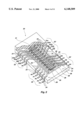
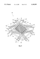
- an inventive die quad-package 60 includes an LOC lead frame 62 comprising an assembly of interdigitated leads 64 supported by a housing 66.
- a portion 62, 62' of each of the leads 64 extends across a front-side surface 73 of an IC die 68 from one edge 67, 69 substantially to another, adjacent edge 71, 72 in close proximity to adjacent leads 64 and adhesively attached to the front-side surface using double-sided adhesive tape 70 so the leads 64 together support the IC die 68 within the die quad-package 60.
- the die quad-package 60 is shown in FIG. 6 in the form of a Thin Quad Flat Pack (TQFP), the present invention is equally applicable to any die quad-package.
- the leads 64 of the LOC lead frame 62 are shown in FIG. 6 having a particular shape and a particular arrangement with respect to one another, it will be understood that the present invention includes within its scope lead frame leads and other support members having any shape and any arrangement that extend substantially from edge to adjacent edge across the front-side surface of an IC die in adhesive attachment therewith.
- such die quad-packages are advantageous because they can be placed on opposing sides of a base, such as a printed circuit Single In-line Memory Module (SIMM) board, with their common pins in alignment, thereby simplifying the routing of signals to the quad-packages.
- SIMM Single In-line Memory Module
- the present invention provides an LOC lead frame and other devices and methods for supporting IC dice in an improved manner.
- the inventive LOC lead frame is capable of producing mirror image die packages, if desired, using identical dice having a wide variety of different bond pad arrangements.
- the inventive lead frame is also capable of conducting heat away from a die in an improved manner.
Abstract
Description
Claims (2)
Priority Applications (1)
| Application Number | Priority Date | Filing Date | Title |
|---|---|---|---|
| US09/141,004 US6148509A (en) | 1997-04-07 | 1998-08-26 | Method for supporting an integrated circuit die |
Applications Claiming Priority (2)
| Application Number | Priority Date | Filing Date | Title |
|---|---|---|---|
| US08/827,886 US6271582B1 (en) | 1997-04-07 | 1997-04-07 | Interdigitated leads-over-chip lead frame, device, and method for supporting an integrated circuit die |
| US09/141,004 US6148509A (en) | 1997-04-07 | 1998-08-26 | Method for supporting an integrated circuit die |
Related Parent Applications (1)
| Application Number | Title | Priority Date | Filing Date |
|---|---|---|---|
| US08/827,886 Division US6271582B1 (en) | 1997-04-07 | 1997-04-07 | Interdigitated leads-over-chip lead frame, device, and method for supporting an integrated circuit die |
Publications (1)
| Publication Number | Publication Date |
|---|---|
| US6148509A true US6148509A (en) | 2000-11-21 |
Family
ID=25250418
Family Applications (8)
| Application Number | Title | Priority Date | Filing Date |
|---|---|---|---|
| US08/827,886 Expired - Lifetime US6271582B1 (en) | 1997-04-07 | 1997-04-07 | Interdigitated leads-over-chip lead frame, device, and method for supporting an integrated circuit die |
| US09/141,004 Expired - Lifetime US6148509A (en) | 1997-04-07 | 1998-08-26 | Method for supporting an integrated circuit die |
| US09/141,002 Expired - Lifetime US5977616A (en) | 1997-04-07 | 1998-08-26 | Interdigitated leads-over-chip lead frame, device, and method for supporting an integrated circuit die |
| US09/141,006 Expired - Lifetime US5973935A (en) | 1997-04-07 | 1998-08-26 | Interdigitated leads-over-chip lead frame for supporting an integrated circuit die |
| US09/141,003 Expired - Lifetime US6107677A (en) | 1997-04-07 | 1998-08-26 | Interdigitated leads-over-chip lead frame, device, and method for supporting an integrated circuit die |
| US09/141,001 Expired - Lifetime US5903443A (en) | 1997-04-07 | 1998-08-26 | Interdigitated leads-over-chip lead frame, device, and method for supporting an integrated circuit die |
| US09/888,885 Expired - Lifetime US6576987B2 (en) | 1997-04-07 | 2001-06-25 | Interdigitated leads-over-chip lead frame, device, and method for supporting an integrated circuit die |
| US10/457,297 Expired - Fee Related US6831353B2 (en) | 1997-04-07 | 2003-06-09 | Interdigitated leads-over-chip lead frame and device for supporting an integrated circuit die |
Family Applications Before (1)
| Application Number | Title | Priority Date | Filing Date |
|---|---|---|---|
| US08/827,886 Expired - Lifetime US6271582B1 (en) | 1997-04-07 | 1997-04-07 | Interdigitated leads-over-chip lead frame, device, and method for supporting an integrated circuit die |
Family Applications After (6)
| Application Number | Title | Priority Date | Filing Date |
|---|---|---|---|
| US09/141,002 Expired - Lifetime US5977616A (en) | 1997-04-07 | 1998-08-26 | Interdigitated leads-over-chip lead frame, device, and method for supporting an integrated circuit die |
| US09/141,006 Expired - Lifetime US5973935A (en) | 1997-04-07 | 1998-08-26 | Interdigitated leads-over-chip lead frame for supporting an integrated circuit die |
| US09/141,003 Expired - Lifetime US6107677A (en) | 1997-04-07 | 1998-08-26 | Interdigitated leads-over-chip lead frame, device, and method for supporting an integrated circuit die |
| US09/141,001 Expired - Lifetime US5903443A (en) | 1997-04-07 | 1998-08-26 | Interdigitated leads-over-chip lead frame, device, and method for supporting an integrated circuit die |
| US09/888,885 Expired - Lifetime US6576987B2 (en) | 1997-04-07 | 2001-06-25 | Interdigitated leads-over-chip lead frame, device, and method for supporting an integrated circuit die |
| US10/457,297 Expired - Fee Related US6831353B2 (en) | 1997-04-07 | 2003-06-09 | Interdigitated leads-over-chip lead frame and device for supporting an integrated circuit die |
Country Status (1)
| Country | Link |
|---|---|
| US (8) | US6271582B1 (en) |
Cited By (66)
| Publication number | Priority date | Publication date | Assignee | Title |
|---|---|---|---|---|
| US6275446B1 (en) | 2000-08-25 | 2001-08-14 | Micron Technology, Inc. | Clock generation circuits and methods |
| US6285074B2 (en) * | 1997-08-25 | 2001-09-04 | Hitachi, Ltd. | Semiconductor device |
| US6445603B1 (en) | 2000-08-21 | 2002-09-03 | Micron Technology, Inc. | Architecture, package orientation and assembly of memory devices |
| US20020140077A1 (en) * | 1998-02-27 | 2002-10-03 | Micron Technology, Inc. | Multichip semiconductor package |
| US6541849B1 (en) | 2000-08-25 | 2003-04-01 | Micron Technology, Inc. | Memory device power distribution |
| US6548376B2 (en) | 2001-08-30 | 2003-04-15 | Micron Technology, Inc. | Methods of thinning microelectronic workpieces |
| US6564979B2 (en) | 2001-07-18 | 2003-05-20 | Micron Technology, Inc. | Method and apparatus for dispensing adhesive on microelectronic substrate supports |
| US20030104654A1 (en) * | 2000-06-28 | 2003-06-05 | Farnworth Warren M. | Recessed encapsulated microelectronic devices and methods for formation |
| US6614092B2 (en) | 2000-08-16 | 2003-09-02 | Micron Technology, Inc. | Microelectronic device package with conductive elements and associated method of manufacture |
| US20030193081A1 (en) * | 1997-04-07 | 2003-10-16 | Aaron Schoenfeld | Interdigitated leads-over-chip lead frame and device for supporting an integrated circuit die |
| US6670719B2 (en) | 1999-08-25 | 2003-12-30 | Micron Technology, Inc. | Microelectronic device package filled with liquid or pressurized gas and associated method of manufacture |
| US6673649B1 (en) | 2002-07-05 | 2004-01-06 | Micron Technology, Inc. | Microelectronic device packages and methods for controlling the disposition of non-conductive materials in such packages |
| US20040026773A1 (en) * | 2002-08-08 | 2004-02-12 | Koon Eng Meow | Packaged microelectronic components |
| US20040026776A1 (en) * | 2002-08-08 | 2004-02-12 | Brand Joseph M. | Microelectronic devices and methods for manufacturing and operating packaged microelectronic device assemblies |
| US20040035917A1 (en) * | 2002-08-22 | 2004-02-26 | Michel Koopmans | Apparatus and method for depositing and reflowing solder paste on a microelectronic workpiece |
| US20040113385A1 (en) * | 2002-11-28 | 2004-06-17 | Shimano, Inc. | Bicycle electronic control device with a reset function |
| US20040159921A1 (en) * | 2001-12-26 | 2004-08-19 | Stephen Moxham | Methods for coupling a flowable conductive material to microelectronic substrates |
| US20040173899A1 (en) * | 2003-03-04 | 2004-09-09 | Peng Neo Chee | Microelectronic component assemblies employing lead frames having reduced-thickness inner lengths |
| US20040178495A1 (en) * | 2003-03-14 | 2004-09-16 | Yean Tay Wuu | Microelectronic devices and methods for packaging microelectronic devices |
| US20040177984A1 (en) * | 2003-03-11 | 2004-09-16 | Groothuis Steven K. | Microelectronic component assemblies having lead frames adapted to reduce package bow |
| US20040238909A1 (en) * | 2003-05-30 | 2004-12-02 | Boon Suan Jeung | Packaged microelectronic devices and methods of packaging microelectronic devices |
| US20050046431A1 (en) * | 2003-09-03 | 2005-03-03 | Kirby Kyle K. | Probe card for use with microelectronic components,and methods for making same |
| US20050045378A1 (en) * | 2003-08-29 | 2005-03-03 | Heng Mung Suan | Stacked microfeature devices and associated methods |
| US6876066B2 (en) | 2001-08-29 | 2005-04-05 | Micron Technology, Inc. | Packaged microelectronic devices and methods of forming same |
| US6879050B2 (en) | 2003-02-11 | 2005-04-12 | Micron Technology, Inc. | Packaged microelectronic devices and methods for packaging microelectronic devices |
| US20050083648A1 (en) * | 2003-10-16 | 2005-04-21 | Janzen Jeffery W. | Methods and apparatuses for transferring heat from microelectronic device modules |
| US20050104228A1 (en) * | 2003-11-13 | 2005-05-19 | Rigg Sidney B. | Microelectronic devices, methods for forming vias in microelectronic devices, and methods for packaging microelectronic devices |
| US20050104171A1 (en) * | 2003-11-13 | 2005-05-19 | Benson Peter A. | Microelectronic devices having conductive complementary structures and methods of manufacturing microelectronic devices having conductive complementary structures |
| US20050156294A1 (en) * | 2003-01-06 | 2005-07-21 | Micron Technology, Inc. | Microelectronic component assemblies and microelectronic component lead frame structures |
| US6951982B2 (en) | 2002-11-22 | 2005-10-04 | Micron Technology, Inc. | Packaged microelectronic component assemblies |
| US20050250251A1 (en) * | 2000-08-23 | 2005-11-10 | Corisis David J | Method and apparatus for decoupling conductive portions of a microelectronic device package |
| US20050281012A1 (en) * | 2004-06-16 | 2005-12-22 | Charles Clark | Mirror image electrical packages and system for using same |
| US20060017177A1 (en) * | 2004-07-23 | 2006-01-26 | Seng Eric T S | Microelectronic component assemblies with recessed wire bonds and methods of making same |
| US20060040428A1 (en) * | 2004-08-19 | 2006-02-23 | Johnson Mark S | Conductive structures for microfeature devices and methods for fabricating microfeature devices |
| US20060044773A1 (en) * | 2004-08-25 | 2006-03-02 | Micron Technology, Inc. | Methods and apparatuses for transferring heat from stacked microfeature devices |
| US20060043611A1 (en) * | 2004-09-01 | 2006-03-02 | Kinsman Larry D | Reduced-dimension microelectronic component assemblies with wire bonds and methods of making same |
| US20060292858A1 (en) * | 2002-07-18 | 2006-12-28 | Micron Technology, Inc. | Techniques to create low K ILD for beol |
| US20070045797A1 (en) * | 2005-08-24 | 2007-03-01 | Micron Technology, Inc. | Microelectronic devices and microelectronic support devices, and associated assemblies and methods |
| US7259451B2 (en) | 2003-08-29 | 2007-08-21 | Micron Technology, Inc. | Invertible microfeature device packages |
| US20070210441A1 (en) * | 2006-03-08 | 2007-09-13 | Micron Technology, Inc. | Microelectronic device assemblies including assemblies with recurved leadframes, and associated methods |
| US7273769B1 (en) | 2000-08-16 | 2007-09-25 | Micron Technology, Inc. | Method and apparatus for removing encapsulating material from a packaged microelectronic device |
| US20080006940A1 (en) * | 2006-07-05 | 2008-01-10 | Micron Technology, Inc. | Lead frames, microelectronic devices with lead frames, and methods for manufacturing lead frames and microelectronic devices with lead frames |
| US20080012110A1 (en) * | 2006-07-17 | 2008-01-17 | Micron Technology, Inc. | Microelectronic packages with leadframes, including leadframes configured for stacked die packages, and associated systems and methods |
| US7425499B2 (en) | 2004-08-24 | 2008-09-16 | Micron Technology, Inc. | Methods for forming interconnects in vias and microelectronic workpieces including such interconnects |
| US20080224291A1 (en) * | 2007-03-13 | 2008-09-18 | Micron Technology, Inc. | Packaged semiconductor components having substantially rigid support members and methods of packaging semiconductor components |
| US7435913B2 (en) | 2004-08-27 | 2008-10-14 | Micron Technology, Inc. | Slanted vias for electrical circuits on circuit boards and other substrates |
| US20090026592A1 (en) * | 2007-07-24 | 2009-01-29 | Micron Technology, Inc. | Semiconductor dies with recesses, associated leadframes, and associated systems and methods |
| US20090026593A1 (en) * | 2007-07-24 | 2009-01-29 | Micron Technology, Inc. | Thin semiconductor die packages and associated systems and methods |
| US7589008B2 (en) | 2004-12-30 | 2009-09-15 | Micron Technology, Inc. | Methods for forming interconnects in microelectronic workpieces and microelectronic workpieces formed using such methods |
| US7629249B2 (en) | 2006-08-28 | 2009-12-08 | Micron Technology, Inc. | Microfeature workpieces having conductive interconnect structures formed by chemically reactive processes, and associated systems and methods |
| US7671459B2 (en) | 2006-02-08 | 2010-03-02 | Micron Technologies, Inc. | Microelectronic devices, stacked microelectronic devices, and methods for manufacturing such devices |
| US7683458B2 (en) | 2004-09-02 | 2010-03-23 | Micron Technology, Inc. | Through-wafer interconnects for photoimager and memory wafers |
| US7749899B2 (en) | 2006-06-01 | 2010-07-06 | Micron Technology, Inc. | Microelectronic workpieces and methods and systems for forming interconnects in microelectronic workpieces |
| US7759221B2 (en) | 2005-12-29 | 2010-07-20 | Micron Technology, Inc. | Methods for packaging microelectronic devices and microelectronic devices formed using such methods |
| US7795134B2 (en) | 2005-06-28 | 2010-09-14 | Micron Technology, Inc. | Conductive interconnect structures and formation methods using supercritical fluids |
| US7829976B2 (en) | 2004-06-29 | 2010-11-09 | Micron Technology, Inc. | Microelectronic devices and methods for forming interconnects in microelectronic devices |
| US7830018B2 (en) | 2007-08-31 | 2010-11-09 | Micron Technology, Inc. | Partitioned through-layer via and associated systems and methods |
| US7843050B2 (en) | 2007-07-24 | 2010-11-30 | Micron Technology, Inc. | Microelectronic die packages with metal leads, including metal leads for stacked die packages, and associated systems and methods |
| US7863187B2 (en) | 2005-09-01 | 2011-01-04 | Micron Technology, Inc. | Microfeature workpieces and methods for forming interconnects in microfeature workpieces |
| US7884015B2 (en) | 2007-12-06 | 2011-02-08 | Micron Technology, Inc. | Methods for forming interconnects in microelectronic workpieces and microelectronic workpieces formed using such methods |
| US7902643B2 (en) | 2006-08-31 | 2011-03-08 | Micron Technology, Inc. | Microfeature workpieces having interconnects and conductive backplanes, and associated systems and methods |
| US7910385B2 (en) | 2006-05-12 | 2011-03-22 | Micron Technology, Inc. | Method of fabricating microelectronic devices |
| US7915736B2 (en) | 2005-09-01 | 2011-03-29 | Micron Technology, Inc. | Microfeature workpieces and methods for forming interconnects in microfeature workpieces |
| US7947529B2 (en) | 2007-08-16 | 2011-05-24 | Micron Technology, Inc. | Microelectronic die packages with leadframes, including leadframe-based interposer for stacked die packages, and associated systems and methods |
| US8084866B2 (en) | 2003-12-10 | 2011-12-27 | Micron Technology, Inc. | Microelectronic devices and methods for filling vias in microelectronic devices |
| US8536485B2 (en) | 2004-05-05 | 2013-09-17 | Micron Technology, Inc. | Systems and methods for forming apertures in microfeature workpieces |
Families Citing this family (111)
| Publication number | Priority date | Publication date | Assignee | Title |
|---|---|---|---|---|
| MY122101A (en) * | 1997-03-28 | 2006-03-31 | Rohm Co Ltd | Lead frame and semiconductor device made by using it |
| JP2954110B2 (en) * | 1997-09-26 | 1999-09-27 | 九州日本電気株式会社 | CSP type semiconductor device and manufacturing method thereof |
| US6144089A (en) | 1997-11-26 | 2000-11-07 | Micron Technology, Inc. | Inner-digitized bond fingers on bus bars of semiconductor device package |
| JP3480291B2 (en) * | 1998-01-08 | 2003-12-15 | 日立電線株式会社 | Semiconductor device and electronic device |
| US6143981A (en) | 1998-06-24 | 2000-11-07 | Amkor Technology, Inc. | Plastic integrated circuit package and method and leadframe for making the package |
| US6260089B1 (en) * | 1998-11-25 | 2001-07-10 | International Business Machines Corporation | Method and apparatus for implementing connections with circuits |
| US6385756B1 (en) * | 1999-03-23 | 2002-05-07 | Conexant Systems, Inc. | Selection of functions within an integrated circuit |
| DE19922186C1 (en) * | 1999-05-12 | 2000-10-19 | Siemens Ag | IC chip with alternate wiring modes |
| US6453547B1 (en) | 1999-11-10 | 2002-09-24 | Micron Technology, Inc. | Coupling spaced bond pads to a contact |
| SG83741A1 (en) * | 1999-08-17 | 2001-10-16 | Micron Technology Inc | Coupling spaced bond pads to a contact |
| US6362429B1 (en) * | 1999-08-18 | 2002-03-26 | Micron Technology, Inc. | Stress relieving tape bonding interconnect |
| US6556030B1 (en) * | 1999-09-01 | 2003-04-29 | Micron Technology, Inc. | Method of forming an electrical contact |
| US6348728B1 (en) | 2000-01-28 | 2002-02-19 | Fujitsu Limited | Semiconductor device having a plurality of semiconductor elements interconnected by a redistribution layer |
| US6791555B1 (en) | 2000-06-23 | 2004-09-14 | Micron Technology, Inc. | Apparatus and method for distributed memory control in a graphics processing system |
| JP2002076233A (en) * | 2000-09-04 | 2002-03-15 | Mitsubishi Electric Corp | Semiconductor device |
| DE10047147B4 (en) * | 2000-09-22 | 2005-04-07 | Infineon Technologies Ag | Integrated semiconductor circuit, in particular semiconductor memory circuit and semiconductor circuit module using same |
| KR100731007B1 (en) * | 2001-01-15 | 2007-06-22 | 앰코 테크놀로지 코리아 주식회사 | stack-type semiconductor package |
| US20040225766A1 (en) * | 2001-01-25 | 2004-11-11 | Ellison Ryan Scott | Functional pathway configuration at a system/IC interface |
| KR100369393B1 (en) | 2001-03-27 | 2003-02-05 | 앰코 테크놀로지 코리아 주식회사 | Lead frame and semiconductor package using it and its manufacturing method |
| US20030033576A1 (en) * | 2001-05-25 | 2003-02-13 | Mark Palmer | Functional pathway configuration at a system/IC interface |
| US20020199159A1 (en) * | 2001-06-22 | 2002-12-26 | Vinson Dong | Naked chip motherboard module |
| DE10243947B4 (en) * | 2001-09-20 | 2007-02-01 | Infineon Technologies Ag | Electronic component with at least one semiconductor chip and method for its production |
| US20040021483A1 (en) * | 2001-09-28 | 2004-02-05 | Brian Boles | Functional pathway configuration at a system/IC interface |
| US20030101312A1 (en) * | 2001-11-26 | 2003-05-29 | Doan Trung T. | Machine state storage apparatus and method |
| US7133972B2 (en) * | 2002-06-07 | 2006-11-07 | Micron Technology, Inc. | Memory hub with internal cache and/or memory access prediction |
| US7157790B2 (en) * | 2002-07-31 | 2007-01-02 | Microchip Technology Inc. | Single die stitch bonding |
| US7326594B2 (en) | 2002-07-31 | 2008-02-05 | Microchip Technology Incorporated | Connecting a plurality of bond pads and/or inner leads with a single bond wire |
| US7200024B2 (en) | 2002-08-02 | 2007-04-03 | Micron Technology, Inc. | System and method for optically interconnecting memory devices |
| US7117316B2 (en) | 2002-08-05 | 2006-10-03 | Micron Technology, Inc. | Memory hub and access method having internal row caching |
| US7254331B2 (en) | 2002-08-09 | 2007-08-07 | Micron Technology, Inc. | System and method for multiple bit optical data transmission in memory systems |
| US7149874B2 (en) | 2002-08-16 | 2006-12-12 | Micron Technology, Inc. | Memory hub bypass circuit and method |
| US6820181B2 (en) | 2002-08-29 | 2004-11-16 | Micron Technology, Inc. | Method and system for controlling memory accesses to memory modules having a memory hub architecture |
| US7836252B2 (en) | 2002-08-29 | 2010-11-16 | Micron Technology, Inc. | System and method for optimizing interconnections of memory devices in a multichip module |
| US7102907B2 (en) | 2002-09-09 | 2006-09-05 | Micron Technology, Inc. | Wavelength division multiplexed memory module, memory system and method |
| KR100475740B1 (en) * | 2003-02-25 | 2005-03-10 | 삼성전자주식회사 | semiconductor intergrated circuit having pads layout for improving signal integrity and for reducing chip size |
| US7245145B2 (en) | 2003-06-11 | 2007-07-17 | Micron Technology, Inc. | Memory module and method having improved signal routing topology |
| US7120727B2 (en) | 2003-06-19 | 2006-10-10 | Micron Technology, Inc. | Reconfigurable memory module and method |
| US7260685B2 (en) | 2003-06-20 | 2007-08-21 | Micron Technology, Inc. | Memory hub and access method having internal prefetch buffers |
| US7107415B2 (en) | 2003-06-20 | 2006-09-12 | Micron Technology, Inc. | Posted write buffers and methods of posting write requests in memory modules |
| US7428644B2 (en) | 2003-06-20 | 2008-09-23 | Micron Technology, Inc. | System and method for selective memory module power management |
| US7389364B2 (en) | 2003-07-22 | 2008-06-17 | Micron Technology, Inc. | Apparatus and method for direct memory access in a hub-based memory system |
| US7210059B2 (en) | 2003-08-19 | 2007-04-24 | Micron Technology, Inc. | System and method for on-board diagnostics of memory modules |
| US7133991B2 (en) | 2003-08-20 | 2006-11-07 | Micron Technology, Inc. | Method and system for capturing and bypassing memory transactions in a hub-based memory system |
| US7136958B2 (en) | 2003-08-28 | 2006-11-14 | Micron Technology, Inc. | Multiple processor system and method including multiple memory hub modules |
| US20050050237A1 (en) * | 2003-08-28 | 2005-03-03 | Jeddeloh Joseph M. | Memory module and method having on-board data search capabilities and processor-based system using such memory modules |
| US7310752B2 (en) | 2003-09-12 | 2007-12-18 | Micron Technology, Inc. | System and method for on-board timing margin testing of memory modules |
| US7194593B2 (en) | 2003-09-18 | 2007-03-20 | Micron Technology, Inc. | Memory hub with integrated non-volatile memory |
| US7120743B2 (en) | 2003-10-20 | 2006-10-10 | Micron Technology, Inc. | Arbitration system and method for memory responses in a hub-based memory system |
| US7038327B2 (en) * | 2003-11-11 | 2006-05-02 | Au Optronics Corp. | Anisotropic conductive film bonding pad |
| US7330992B2 (en) | 2003-12-29 | 2008-02-12 | Micron Technology, Inc. | System and method for read synchronization of memory modules |
| TWI237889B (en) * | 2004-01-16 | 2005-08-11 | Optimum Care Int Tech Inc | Chip leadframe module |
| US7188219B2 (en) | 2004-01-30 | 2007-03-06 | Micron Technology, Inc. | Buffer control system and method for a memory system having outstanding read and write request buffers |
| US7412574B2 (en) | 2004-02-05 | 2008-08-12 | Micron Technology, Inc. | System and method for arbitration of memory responses in a hub-based memory system |
| US7788451B2 (en) | 2004-02-05 | 2010-08-31 | Micron Technology, Inc. | Apparatus and method for data bypass for a bi-directional data bus in a hub-based memory sub-system |
| US7181584B2 (en) | 2004-02-05 | 2007-02-20 | Micron Technology, Inc. | Dynamic command and/or address mirroring system and method for memory modules |
| US7366864B2 (en) | 2004-03-08 | 2008-04-29 | Micron Technology, Inc. | Memory hub architecture having programmable lane widths |
| US6929485B1 (en) | 2004-03-16 | 2005-08-16 | Agilent Technologies, Inc. | Lead frame with interdigitated pins |
| US7257683B2 (en) | 2004-03-24 | 2007-08-14 | Micron Technology, Inc. | Memory arbitration system and method having an arbitration packet protocol |
| US7120723B2 (en) | 2004-03-25 | 2006-10-10 | Micron Technology, Inc. | System and method for memory hub-based expansion bus |
| US7213082B2 (en) | 2004-03-29 | 2007-05-01 | Micron Technology, Inc. | Memory hub and method for providing memory sequencing hints |
| US7447240B2 (en) | 2004-03-29 | 2008-11-04 | Micron Technology, Inc. | Method and system for synchronizing communications links in a hub-based memory system |
| US6980042B2 (en) | 2004-04-05 | 2005-12-27 | Micron Technology, Inc. | Delay line synchronizer apparatus and method |
| US7590797B2 (en) | 2004-04-08 | 2009-09-15 | Micron Technology, Inc. | System and method for optimizing interconnections of components in a multichip memory module |
| US7162567B2 (en) | 2004-05-14 | 2007-01-09 | Micron Technology, Inc. | Memory hub and method for memory sequencing |
| US7222213B2 (en) | 2004-05-17 | 2007-05-22 | Micron Technology, Inc. | System and method for communicating the synchronization status of memory modules during initialization of the memory modules |
| US7363419B2 (en) | 2004-05-28 | 2008-04-22 | Micron Technology, Inc. | Method and system for terminating write commands in a hub-based memory system |
| US7519788B2 (en) | 2004-06-04 | 2009-04-14 | Micron Technology, Inc. | System and method for an asynchronous data buffer having buffer write and read pointers |
| US7310748B2 (en) | 2004-06-04 | 2007-12-18 | Micron Technology, Inc. | Memory hub tester interface and method for use thereof |
| US7392331B2 (en) | 2004-08-31 | 2008-06-24 | Micron Technology, Inc. | System and method for transmitting data packets in a computer system having a memory hub architecture |
| US7507603B1 (en) | 2005-12-02 | 2009-03-24 | Amkor Technology, Inc. | Etch singulated semiconductor package |
| US7968998B1 (en) | 2006-06-21 | 2011-06-28 | Amkor Technology, Inc. | Side leaded, bottom exposed pad and bottom exposed lead fusion quad flat semiconductor package |
| US20080079124A1 (en) * | 2006-10-03 | 2008-04-03 | Chris Edward Haga | Interdigitated leadfingers |
| JP2008102345A (en) * | 2006-10-19 | 2008-05-01 | Nec Electronics Corp | Semiconductor integrated circuit device |
| US7982297B1 (en) | 2007-03-06 | 2011-07-19 | Amkor Technology, Inc. | Stackable semiconductor package having partially exposed semiconductor die and method of fabricating the same |
| JP5004654B2 (en) * | 2007-05-16 | 2012-08-22 | パナソニック株式会社 | Wiring board connection method and wiring board structure |
| US8058099B2 (en) * | 2007-06-28 | 2011-11-15 | Sandisk Technologies Inc. | Method of fabricating a two-sided die in a four-sided leadframe based package |
| US8395246B2 (en) * | 2007-06-28 | 2013-03-12 | Sandisk Technologies Inc. | Two-sided die in a four-sided leadframe based package |
| US7977774B2 (en) | 2007-07-10 | 2011-07-12 | Amkor Technology, Inc. | Fusion quad flat semiconductor package |
| US7687899B1 (en) | 2007-08-07 | 2010-03-30 | Amkor Technology, Inc. | Dual laminate package structure with embedded elements |
| US7777351B1 (en) | 2007-10-01 | 2010-08-17 | Amkor Technology, Inc. | Thin stacked interposer package |
| US8089159B1 (en) | 2007-10-03 | 2012-01-03 | Amkor Technology, Inc. | Semiconductor package with increased I/O density and method of making the same |
| US7847386B1 (en) | 2007-11-05 | 2010-12-07 | Amkor Technology, Inc. | Reduced size stacked semiconductor package and method of making the same |
| US7956453B1 (en) | 2008-01-16 | 2011-06-07 | Amkor Technology, Inc. | Semiconductor package with patterning layer and method of making same |
| US7723852B1 (en) | 2008-01-21 | 2010-05-25 | Amkor Technology, Inc. | Stacked semiconductor package and method of making same |
| US8067821B1 (en) | 2008-04-10 | 2011-11-29 | Amkor Technology, Inc. | Flat semiconductor package with half package molding |
| US7768135B1 (en) | 2008-04-17 | 2010-08-03 | Amkor Technology, Inc. | Semiconductor package with fast power-up cycle and method of making same |
| US7808084B1 (en) | 2008-05-06 | 2010-10-05 | Amkor Technology, Inc. | Semiconductor package with half-etched locking features |
| US8125064B1 (en) | 2008-07-28 | 2012-02-28 | Amkor Technology, Inc. | Increased I/O semiconductor package and method of making same |
| US8184453B1 (en) | 2008-07-31 | 2012-05-22 | Amkor Technology, Inc. | Increased capacity semiconductor package |
| US8174099B2 (en) * | 2008-08-13 | 2012-05-08 | Atmel Corporation | Leadless package with internally extended package leads |
| US7847392B1 (en) | 2008-09-30 | 2010-12-07 | Amkor Technology, Inc. | Semiconductor device including leadframe with increased I/O |
| US7989933B1 (en) | 2008-10-06 | 2011-08-02 | Amkor Technology, Inc. | Increased I/O leadframe and semiconductor device including same |
| US8008758B1 (en) | 2008-10-27 | 2011-08-30 | Amkor Technology, Inc. | Semiconductor device with increased I/O leadframe |
| US8089145B1 (en) | 2008-11-17 | 2012-01-03 | Amkor Technology, Inc. | Semiconductor device including increased capacity leadframe |
| US8072050B1 (en) | 2008-11-18 | 2011-12-06 | Amkor Technology, Inc. | Semiconductor device with increased I/O leadframe including passive device |
| US7875963B1 (en) | 2008-11-21 | 2011-01-25 | Amkor Technology, Inc. | Semiconductor device including leadframe having power bars and increased I/O |
| US7982298B1 (en) | 2008-12-03 | 2011-07-19 | Amkor Technology, Inc. | Package in package semiconductor device |
| US8487420B1 (en) | 2008-12-08 | 2013-07-16 | Amkor Technology, Inc. | Package in package semiconductor device with film over wire |
| US8680656B1 (en) | 2009-01-05 | 2014-03-25 | Amkor Technology, Inc. | Leadframe structure for concentrated photovoltaic receiver package |
| US20170117214A1 (en) | 2009-01-05 | 2017-04-27 | Amkor Technology, Inc. | Semiconductor device with through-mold via |
| US8058715B1 (en) | 2009-01-09 | 2011-11-15 | Amkor Technology, Inc. | Package in package device for RF transceiver module |
| US8026589B1 (en) | 2009-02-23 | 2011-09-27 | Amkor Technology, Inc. | Reduced profile stackable semiconductor package |
| US7960818B1 (en) | 2009-03-04 | 2011-06-14 | Amkor Technology, Inc. | Conformal shield on punch QFN semiconductor package |
| US8575742B1 (en) | 2009-04-06 | 2013-11-05 | Amkor Technology, Inc. | Semiconductor device with increased I/O leadframe including power bars |
| TWI557183B (en) | 2015-12-16 | 2016-11-11 | 財團法人工業技術研究院 | Siloxane resin composition, and photoelectric device employing the same |
| US8648450B1 (en) | 2011-01-27 | 2014-02-11 | Amkor Technology, Inc. | Semiconductor device including leadframe with a combination of leads and lands |
| US9704725B1 (en) | 2012-03-06 | 2017-07-11 | Amkor Technology, Inc. | Semiconductor device with leadframe configured to facilitate reduced burr formation |
| KR101486790B1 (en) | 2013-05-02 | 2015-01-28 | 앰코 테크놀로지 코리아 주식회사 | Micro Lead Frame for semiconductor package |
| KR101563911B1 (en) | 2013-10-24 | 2015-10-28 | 앰코 테크놀로지 코리아 주식회사 | Semiconductor package |
| US9673122B2 (en) | 2014-05-02 | 2017-06-06 | Amkor Technology, Inc. | Micro lead frame structure having reinforcing portions and method |
| US20170245361A1 (en) * | 2016-01-06 | 2017-08-24 | Nokomis, Inc. | Electronic device and methods to customize electronic device electromagnetic emissions |
Citations (30)
| Publication number | Priority date | Publication date | Assignee | Title |
|---|---|---|---|---|
| US4862245A (en) * | 1985-04-18 | 1989-08-29 | International Business Machines Corporation | Package semiconductor chip |
| US4937656A (en) * | 1988-04-22 | 1990-06-26 | Mitsubishi Denki Kabushiki Kaisha | Semiconductor device |
| US4949161A (en) * | 1988-12-23 | 1990-08-14 | Micron Technology, Inc. | Interdigitized leadframe strip |
| US5086018A (en) * | 1991-05-02 | 1992-02-04 | International Business Machines Corporation | Method of making a planarized thin film covered wire bonded semiconductor package |
| US5147815A (en) * | 1990-05-14 | 1992-09-15 | Motorola, Inc. | Method for fabricating a multichip semiconductor device having two interdigitated leadframes |
| JPH05109979A (en) * | 1991-10-15 | 1993-04-30 | Mitsubishi Electric Corp | Manufacture of inverting type ic and ic module using the same |
| US5218168A (en) * | 1991-09-26 | 1993-06-08 | Micron Technology, Inc. | Leads over tab |
| US5234866A (en) * | 1985-03-25 | 1993-08-10 | Hitachi, Ltd. | Semiconductor device and process for producing the same, and lead frame used in said process |
| US5250840A (en) * | 1992-02-24 | 1993-10-05 | Samsung Electronics Co., Ltd. | Semiconductor lead frame with a chip having bonding pads in a cross arrangement |
| US5256598A (en) * | 1992-04-15 | 1993-10-26 | Micron Technology, Inc. | Shrink accommodating lead frame |
| US5327009A (en) * | 1992-05-22 | 1994-07-05 | Nec Corporation | Miniaturized integrated circuit package |
| US5331200A (en) * | 1992-09-30 | 1994-07-19 | Texas Instruments Incorporated | Lead-on-chip inner lead bonding lead frame method and apparatus |
| US5360992A (en) * | 1991-12-20 | 1994-11-01 | Micron Technology, Inc. | Two piece assembly for the selection of pinouts and bond options on a semiconductor device |
| US5381036A (en) * | 1992-02-03 | 1995-01-10 | Motorola, Inc. | Lead-on chip semiconductor device having peripheral bond pads |
| US5384488A (en) * | 1992-06-15 | 1995-01-24 | Texas Instruments Incorporated | Configuration and method for positioning semiconductor device bond pads using additional process layers |
| US5434106A (en) * | 1989-12-22 | 1995-07-18 | Texas Instruments Incorporated | Integrated circuit device and method to prevent cracking during surface mount |
| US5438478A (en) * | 1992-10-20 | 1995-08-01 | Ibiden Co., Ltd. | Electronic component carriers and method of producing the same as well as electronic devices |
| US5508565A (en) * | 1992-12-18 | 1996-04-16 | Fujitsu Limited | Semiconductor device having a plurality of chips having identical circuit arrangement sealed in package |
| US5521426A (en) * | 1992-09-09 | 1996-05-28 | Texas Instruments Incorporated | Reduced capacitance lead frame for lead on chip package |
| US5523617A (en) * | 1994-12-27 | 1996-06-04 | National Semiconductor Corporation | Fuse frames, programmable fuse frames, and methods for programming by fusing |
| US5528075A (en) * | 1991-08-15 | 1996-06-18 | Staktek Corporation | Lead-on-chip integrated circuit apparatus |
| US5530292A (en) * | 1990-03-15 | 1996-06-25 | Fujitsu Limited | Semiconductor device having a plurality of chips |
| US5563443A (en) * | 1993-03-13 | 1996-10-08 | Texas Instruments Incorporated | Packaged semiconductor device utilizing leadframe attached on a semiconductor chip |
| US5585667A (en) * | 1994-12-23 | 1996-12-17 | National Semiconductor Corporation | Lead frame for handling crossing bonding wires |
| US5585668A (en) * | 1995-01-30 | 1996-12-17 | Staktek Corporation | Integrated circuit package with overlapped die on a common lead frame |
| US5612259A (en) * | 1993-07-29 | 1997-03-18 | Kabushiki Kaisha Toshiba | Method for manufacturing a semiconductor device wherein a semiconductor chip is mounted on a lead frame |
| US5637915A (en) * | 1991-12-27 | 1997-06-10 | Fujitsu Ltd. | Semiconductor device affixed to an upper and a lower leadframe |
| US5696665A (en) * | 1994-07-01 | 1997-12-09 | Saint-Gobain/Norton Industrial Ceramics Corporation | Integrated circuit package with diamond heat sink |
| US5780925A (en) * | 1992-10-28 | 1998-07-14 | International Business Machines Corporation | Lead frame package for electronic devices |
| US5804870A (en) * | 1992-06-26 | 1998-09-08 | Staktek Corporation | Hermetically sealed integrated circuit lead-on package configuration |
Family Cites Families (11)
| Publication number | Priority date | Publication date | Assignee | Title |
|---|---|---|---|---|
| JPH06105721B2 (en) * | 1985-03-25 | 1994-12-21 | 日立超エル・エス・アイエンジニアリング株式会社 | Semiconductor device |
| US5365113A (en) | 1987-06-30 | 1994-11-15 | Hitachi, Ltd. | Semiconductor device |
| JP2528991B2 (en) | 1990-02-28 | 1996-08-28 | 株式会社日立製作所 | Resin-sealed semiconductor device and lead frame |
| KR940006164B1 (en) | 1991-05-11 | 1994-07-08 | 금성일렉트론 주식회사 | Semiconductor device and manufacturing method thereof |
| US5254598A (en) * | 1991-12-09 | 1993-10-19 | Southwest Research Institute | Biodegradable composition and products |
| US5811875A (en) | 1995-06-29 | 1998-09-22 | Samsung Electronics Co., Ltd. | Lead frames including extended tie-bars, and semiconductor chip packages using same |
| JPH09102575A (en) | 1995-09-11 | 1997-04-15 | Internatl Business Mach Corp <Ibm> | Lead frame structure of lead-on chip without jump on wiring |
| US6462404B1 (en) | 1997-02-28 | 2002-10-08 | Micron Technology, Inc. | Multilevel leadframe for a packaged integrated circuit |
| US6271582B1 (en) * | 1997-04-07 | 2001-08-07 | Micron Technology, Inc. | Interdigitated leads-over-chip lead frame, device, and method for supporting an integrated circuit die |
| US6008996A (en) * | 1997-04-07 | 1999-12-28 | Micron Technology, Inc. | Interdigitated leads-over-chip lead frame, device, and method for supporting an integrated circuit die |
| US6052289A (en) * | 1998-08-26 | 2000-04-18 | Micron Technology, Inc. | Interdigitated leads-over-chip lead frame for supporting an integrated circuit die |
-
1997
- 1997-04-07 US US08/827,886 patent/US6271582B1/en not_active Expired - Lifetime
-
1998
- 1998-08-26 US US09/141,004 patent/US6148509A/en not_active Expired - Lifetime
- 1998-08-26 US US09/141,002 patent/US5977616A/en not_active Expired - Lifetime
- 1998-08-26 US US09/141,006 patent/US5973935A/en not_active Expired - Lifetime
- 1998-08-26 US US09/141,003 patent/US6107677A/en not_active Expired - Lifetime
- 1998-08-26 US US09/141,001 patent/US5903443A/en not_active Expired - Lifetime
-
2001
- 2001-06-25 US US09/888,885 patent/US6576987B2/en not_active Expired - Lifetime
-
2003
- 2003-06-09 US US10/457,297 patent/US6831353B2/en not_active Expired - Fee Related
Patent Citations (31)
| Publication number | Priority date | Publication date | Assignee | Title |
|---|---|---|---|---|
| US5234866A (en) * | 1985-03-25 | 1993-08-10 | Hitachi, Ltd. | Semiconductor device and process for producing the same, and lead frame used in said process |
| US4862245A (en) * | 1985-04-18 | 1989-08-29 | International Business Machines Corporation | Package semiconductor chip |
| US4937656A (en) * | 1988-04-22 | 1990-06-26 | Mitsubishi Denki Kabushiki Kaisha | Semiconductor device |
| US4949161A (en) * | 1988-12-23 | 1990-08-14 | Micron Technology, Inc. | Interdigitized leadframe strip |
| US5434106A (en) * | 1989-12-22 | 1995-07-18 | Texas Instruments Incorporated | Integrated circuit device and method to prevent cracking during surface mount |
| US5530292A (en) * | 1990-03-15 | 1996-06-25 | Fujitsu Limited | Semiconductor device having a plurality of chips |
| US5147815A (en) * | 1990-05-14 | 1992-09-15 | Motorola, Inc. | Method for fabricating a multichip semiconductor device having two interdigitated leadframes |
| US5086018A (en) * | 1991-05-02 | 1992-02-04 | International Business Machines Corporation | Method of making a planarized thin film covered wire bonded semiconductor package |
| US5528075A (en) * | 1991-08-15 | 1996-06-18 | Staktek Corporation | Lead-on-chip integrated circuit apparatus |
| US5218168A (en) * | 1991-09-26 | 1993-06-08 | Micron Technology, Inc. | Leads over tab |
| US5303120A (en) * | 1991-10-15 | 1994-04-12 | Mitsubishi Denki Kabushiki Kaisha | Method of manufacturing inversion type IC's and IC module using same |
| JPH05109979A (en) * | 1991-10-15 | 1993-04-30 | Mitsubishi Electric Corp | Manufacture of inverting type ic and ic module using the same |
| US5360992A (en) * | 1991-12-20 | 1994-11-01 | Micron Technology, Inc. | Two piece assembly for the selection of pinouts and bond options on a semiconductor device |
| US5637915A (en) * | 1991-12-27 | 1997-06-10 | Fujitsu Ltd. | Semiconductor device affixed to an upper and a lower leadframe |
| US5381036A (en) * | 1992-02-03 | 1995-01-10 | Motorola, Inc. | Lead-on chip semiconductor device having peripheral bond pads |
| US5250840A (en) * | 1992-02-24 | 1993-10-05 | Samsung Electronics Co., Ltd. | Semiconductor lead frame with a chip having bonding pads in a cross arrangement |
| US5256598A (en) * | 1992-04-15 | 1993-10-26 | Micron Technology, Inc. | Shrink accommodating lead frame |
| US5327009A (en) * | 1992-05-22 | 1994-07-05 | Nec Corporation | Miniaturized integrated circuit package |
| US5384488A (en) * | 1992-06-15 | 1995-01-24 | Texas Instruments Incorporated | Configuration and method for positioning semiconductor device bond pads using additional process layers |
| US5804870A (en) * | 1992-06-26 | 1998-09-08 | Staktek Corporation | Hermetically sealed integrated circuit lead-on package configuration |
| US5521426A (en) * | 1992-09-09 | 1996-05-28 | Texas Instruments Incorporated | Reduced capacitance lead frame for lead on chip package |
| US5331200A (en) * | 1992-09-30 | 1994-07-19 | Texas Instruments Incorporated | Lead-on-chip inner lead bonding lead frame method and apparatus |
| US5438478A (en) * | 1992-10-20 | 1995-08-01 | Ibiden Co., Ltd. | Electronic component carriers and method of producing the same as well as electronic devices |
| US5780925A (en) * | 1992-10-28 | 1998-07-14 | International Business Machines Corporation | Lead frame package for electronic devices |
| US5508565A (en) * | 1992-12-18 | 1996-04-16 | Fujitsu Limited | Semiconductor device having a plurality of chips having identical circuit arrangement sealed in package |
| US5563443A (en) * | 1993-03-13 | 1996-10-08 | Texas Instruments Incorporated | Packaged semiconductor device utilizing leadframe attached on a semiconductor chip |
| US5612259A (en) * | 1993-07-29 | 1997-03-18 | Kabushiki Kaisha Toshiba | Method for manufacturing a semiconductor device wherein a semiconductor chip is mounted on a lead frame |
| US5696665A (en) * | 1994-07-01 | 1997-12-09 | Saint-Gobain/Norton Industrial Ceramics Corporation | Integrated circuit package with diamond heat sink |
| US5585667A (en) * | 1994-12-23 | 1996-12-17 | National Semiconductor Corporation | Lead frame for handling crossing bonding wires |
| US5523617A (en) * | 1994-12-27 | 1996-06-04 | National Semiconductor Corporation | Fuse frames, programmable fuse frames, and methods for programming by fusing |
| US5585668A (en) * | 1995-01-30 | 1996-12-17 | Staktek Corporation | Integrated circuit package with overlapped die on a common lead frame |
Cited By (218)
| Publication number | Priority date | Publication date | Assignee | Title |
|---|---|---|---|---|
| US20030193081A1 (en) * | 1997-04-07 | 2003-10-16 | Aaron Schoenfeld | Interdigitated leads-over-chip lead frame and device for supporting an integrated circuit die |
| US6831353B2 (en) | 1997-04-07 | 2004-12-14 | Micron Technology, Inc. | Interdigitated leads-over-chip lead frame and device for supporting an integrated circuit die |
| US6285074B2 (en) * | 1997-08-25 | 2001-09-04 | Hitachi, Ltd. | Semiconductor device |
| US6297545B1 (en) * | 1997-08-25 | 2001-10-02 | Hitachi, Ltd. | Semiconductor device |
| US20020140077A1 (en) * | 1998-02-27 | 2002-10-03 | Micron Technology, Inc. | Multichip semiconductor package |
| US20050212143A1 (en) * | 1998-02-27 | 2005-09-29 | Micron Technology, Inc. | Multichip semiconductor package |
| US6906409B2 (en) | 1998-02-27 | 2005-06-14 | Micron Technology, Inc. | Multichip semiconductor package |
| US6670719B2 (en) | 1999-08-25 | 2003-12-30 | Micron Technology, Inc. | Microelectronic device package filled with liquid or pressurized gas and associated method of manufacture |
| US6909171B2 (en) | 1999-08-25 | 2005-06-21 | Micron Technology, Inc. | Microelectronic device package filled with liquid or pressurized gas and associated method of manufacture |
| US20030104654A1 (en) * | 2000-06-28 | 2003-06-05 | Farnworth Warren M. | Recessed encapsulated microelectronic devices and methods for formation |
| US6819003B2 (en) | 2000-06-28 | 2004-11-16 | Micron Technology Inc. | Recessed encapsulated microelectronic devices and methods for formation |
| US6841423B2 (en) | 2000-06-28 | 2005-01-11 | Micron Technology, Inc. | Methods for formation of recessed encapsulated microelectronic devices |
| US7405487B2 (en) | 2000-08-16 | 2008-07-29 | Micron Technology, Inc. | Method and apparatus for removing encapsulating material from a packaged microelectronic device |
| US6709968B1 (en) | 2000-08-16 | 2004-03-23 | Micron Technology, Inc. | Microelectronic device with package with conductive elements and associated method of manufacture |
| US7273769B1 (en) | 2000-08-16 | 2007-09-25 | Micron Technology, Inc. | Method and apparatus for removing encapsulating material from a packaged microelectronic device |
| US6614092B2 (en) | 2000-08-16 | 2003-09-02 | Micron Technology, Inc. | Microelectronic device package with conductive elements and associated method of manufacture |
| US6566738B2 (en) | 2000-08-21 | 2003-05-20 | Micron Technology, Inc. | Lead-over-chip leadframes |
| US6625048B2 (en) | 2000-08-21 | 2003-09-23 | Micro Technology, Inc. | Architecture, package orientation and assembly of memory devices |
| US6445603B1 (en) | 2000-08-21 | 2002-09-03 | Micron Technology, Inc. | Architecture, package orientation and assembly of memory devices |
| US20050250251A1 (en) * | 2000-08-23 | 2005-11-10 | Corisis David J | Method and apparatus for decoupling conductive portions of a microelectronic device package |
| US7378723B2 (en) | 2000-08-23 | 2008-05-27 | Micron Technology, Inc. | Method and apparatus for decoupling conductive portions of a microelectronic device package |
| US20070052087A1 (en) * | 2000-08-23 | 2007-03-08 | Micron Technology, Inc. | Method and apparatus for decoupling conductive portions of a microelectronic device package |
| US7183138B2 (en) | 2000-08-23 | 2007-02-27 | Micron Technology, Inc. | Method and apparatus for decoupling conductive portions of a microelectronic device package |
| US6275446B1 (en) | 2000-08-25 | 2001-08-14 | Micron Technology, Inc. | Clock generation circuits and methods |
| US6541849B1 (en) | 2000-08-25 | 2003-04-01 | Micron Technology, Inc. | Memory device power distribution |
| US20060186530A1 (en) * | 2000-08-25 | 2006-08-24 | Micron Technology, Inc. | Memory device power distribution in memory assemblies |
| US20030107123A1 (en) * | 2000-08-25 | 2003-06-12 | Micron Technology, Inc. | Memory device power distribution in memory assemblies |
| US6952045B2 (en) | 2000-08-25 | 2005-10-04 | Micron Technology, Inc. | Memory device power distribution in electronic systems |
| US6456562B1 (en) | 2000-08-25 | 2002-09-24 | Micron Technology, Inc. | Clock generation circuits |
| US20030107122A1 (en) * | 2000-08-25 | 2003-06-12 | Micron Technology, Inc. | Memory device power distribution in electronic systems |
| US7274086B2 (en) | 2000-08-25 | 2007-09-25 | Micron Technology, Inc. | Memory device power distribution in memory assemblies |
| US6949813B2 (en) * | 2000-08-25 | 2005-09-27 | Micron Technology, Inc. | Lead-over-chip lead frames |
| US20060001131A1 (en) * | 2000-08-25 | 2006-01-05 | Micron Technology, Inc. | Memory device power distribution in memory assemblies |
| US20030107121A1 (en) * | 2000-08-25 | 2003-06-12 | Micron Technology, Inc. | LOC leadframe |
| US6564979B2 (en) | 2001-07-18 | 2003-05-20 | Micron Technology, Inc. | Method and apparatus for dispensing adhesive on microelectronic substrate supports |
| US6943450B2 (en) | 2001-08-29 | 2005-09-13 | Micron Technology, Inc. | Packaged microelectronic devices and methods of forming same |
| US6876066B2 (en) | 2001-08-29 | 2005-04-05 | Micron Technology, Inc. | Packaged microelectronic devices and methods of forming same |
| US6548376B2 (en) | 2001-08-30 | 2003-04-15 | Micron Technology, Inc. | Methods of thinning microelectronic workpieces |
| US6936916B2 (en) | 2001-12-26 | 2005-08-30 | Micron Technology, Inc. | Microelectronic assemblies and electronic devices including connection structures with multiple elongated members |
| US6995026B2 (en) | 2001-12-26 | 2006-02-07 | Micron Technology, Inc. | Methods for coupling a flowable conductive material to microelectronic substrates |
| US6870276B1 (en) | 2001-12-26 | 2005-03-22 | Micron Technology, Inc. | Apparatus for supporting microelectronic substrates |
| US20050242437A1 (en) * | 2001-12-26 | 2005-11-03 | Micron Technology, Inc. | Method and apparatus for supporting microelectronic substrates |
| US20040159946A1 (en) * | 2001-12-26 | 2004-08-19 | Stephen Moxham | Microelectronic assemblies, electronic devices, and apparatuses for supporting microelectronic substrates |
| US20040159921A1 (en) * | 2001-12-26 | 2004-08-19 | Stephen Moxham | Methods for coupling a flowable conductive material to microelectronic substrates |
| US20060057774A1 (en) * | 2002-07-05 | 2006-03-16 | Hiatt William M | Microelectronic device packages and methods for controlling the disposition of non-conductive materials in such packages |
| US6673649B1 (en) | 2002-07-05 | 2004-01-06 | Micron Technology, Inc. | Microelectronic device packages and methods for controlling the disposition of non-conductive materials in such packages |
| US7087995B2 (en) | 2002-07-05 | 2006-08-08 | Micron Technology, Inc. | Microelectronic device packages and methods for controlling the disposition of non-conductive materials in such packages |
| US7470563B2 (en) | 2002-07-05 | 2008-12-30 | Micron Technology, Inc. | Microelectronic device packages and methods for controlling the disposition of non-conductive materials in such packages |
| US20040101991A1 (en) * | 2002-07-05 | 2004-05-27 | Hiatt William Mark | Microelectronic device packages and methods for controlling the disposition of non-conductive materials in such packages |
| US20060292858A1 (en) * | 2002-07-18 | 2006-12-28 | Micron Technology, Inc. | Techniques to create low K ILD for beol |
| US7306974B2 (en) | 2002-08-08 | 2007-12-11 | Micron Technology, Inc. | Microelectronic devices and methods for manufacturing and operating packaged microelectronic device assemblies |
| US7067905B2 (en) | 2002-08-08 | 2006-06-27 | Micron Technology, Inc. | Packaged microelectronic devices including first and second casings |
| US7195957B2 (en) | 2002-08-08 | 2007-03-27 | Micron Technology, Inc. | Packaged microelectronic components |
| US20040026773A1 (en) * | 2002-08-08 | 2004-02-12 | Koon Eng Meow | Packaged microelectronic components |
| US20040026776A1 (en) * | 2002-08-08 | 2004-02-12 | Brand Joseph M. | Microelectronic devices and methods for manufacturing and operating packaged microelectronic device assemblies |
| US9418872B2 (en) | 2002-08-08 | 2016-08-16 | Micron Technology, Inc. | Packaged microelectronic components |
| US20060040422A1 (en) * | 2002-08-08 | 2006-02-23 | Micron Technology, Inc. | Microelectronic devices and methods for manufacturing and operating packaged microelectronic device |
| US8637973B2 (en) | 2002-08-08 | 2014-01-28 | Micron Technology, Inc. | Packaged microelectronic components with terminals exposed through encapsulant |
| US20080164298A1 (en) * | 2002-08-22 | 2008-07-10 | Micron Technology, Inc. | Apparatus and method for depositing and reflowing solder paste on a microelectronic workpiece |
| US7347348B2 (en) | 2002-08-22 | 2008-03-25 | Micron Technology, Inc. | Apparatus and method for depositing and reflowing solder paste on a microelectronic workpiece |
| US20040035917A1 (en) * | 2002-08-22 | 2004-02-26 | Michel Koopmans | Apparatus and method for depositing and reflowing solder paste on a microelectronic workpiece |
| US6845901B2 (en) | 2002-08-22 | 2005-01-25 | Micron Technology, Inc. | Apparatus and method for depositing and reflowing solder paste on a microelectronic workpiece |
| US20050092810A1 (en) * | 2002-08-22 | 2005-05-05 | Michel Koopmans | Apparatus and method for depositing and reflowing solder paste on a microelectronic workpiece |
| US7637412B2 (en) | 2002-08-22 | 2009-12-29 | Micron Technology, Inc. | Apparatus and method for depositing and reflowing solder paste on a microelectronic workpiece |
| US6951982B2 (en) | 2002-11-22 | 2005-10-04 | Micron Technology, Inc. | Packaged microelectronic component assemblies |
| US20040113385A1 (en) * | 2002-11-28 | 2004-06-17 | Shimano, Inc. | Bicycle electronic control device with a reset function |
| US20050156300A1 (en) * | 2003-01-06 | 2005-07-21 | Micron Technology, Inc. | Microelectronic component assemblies and microelectronic component lead frame structures |
| US7247520B2 (en) | 2003-01-06 | 2007-07-24 | Micron Technology, Inc. | Microelectronic component assemblies and microelectronic component lead frame structures |
| US20050156294A1 (en) * | 2003-01-06 | 2005-07-21 | Micron Technology, Inc. | Microelectronic component assemblies and microelectronic component lead frame structures |
| US7923824B2 (en) | 2003-01-06 | 2011-04-12 | Micron Technology, Inc. | Microelectronic component assemblies and microelectronic component lead frame structures |
| US7132734B2 (en) | 2003-01-06 | 2006-11-07 | Micron Technology, Inc. | Microelectronic component assemblies and microelectronic component lead frame structures |
| US7298025B2 (en) | 2003-01-06 | 2007-11-20 | Micron Technology, Inc. | Microelectronic component assemblies and microelectronic component lead frame structures |
| US7652365B2 (en) | 2003-01-06 | 2010-01-26 | Micron Technologies, Inc. | Microelectronic component assemblies and microelectronic component lead frame structures |
| US20080067644A1 (en) * | 2003-01-06 | 2008-03-20 | Micron Technology, Inc. | Microelectronic component assemblies and microelectronic component lead frame structures |
| US6879050B2 (en) | 2003-02-11 | 2005-04-12 | Micron Technology, Inc. | Packaged microelectronic devices and methods for packaging microelectronic devices |
| US20040173899A1 (en) * | 2003-03-04 | 2004-09-09 | Peng Neo Chee | Microelectronic component assemblies employing lead frames having reduced-thickness inner lengths |
| US7057281B2 (en) | 2003-03-04 | 2006-06-06 | Micron Technology Inc. | Microelectronic component assemblies employing lead frames having reduced-thickness inner lengths |
| US7425470B2 (en) | 2003-03-04 | 2008-09-16 | Micron Technology, Inc. | Microelectronic component assemblies employing lead frames having reduced-thickness inner lengths |
| US7691680B2 (en) | 2003-03-04 | 2010-04-06 | Micron Technologies, Inc. | Method of fabricating microelectronic component assemblies employing lead frames having reduced-thickness inner lengths |
| US20040177984A1 (en) * | 2003-03-11 | 2004-09-16 | Groothuis Steven K. | Microelectronic component assemblies having lead frames adapted to reduce package bow |
| US20070128770A1 (en) * | 2003-03-11 | 2007-06-07 | Micron Technology, Inc. | Microelectronic component assemblies having lead frames adapted to reduce package bow |
| US7183485B2 (en) | 2003-03-11 | 2007-02-27 | Micron Technology, Inc. | Microelectronic component assemblies having lead frames adapted to reduce package bow |
| US20070128737A1 (en) * | 2003-03-14 | 2007-06-07 | Micron Technology, Inc. | Microelectronic devices and methods for packaging microelectronic devices |
| US20060006534A1 (en) * | 2003-03-14 | 2006-01-12 | Yean Tay W | Microelectronic devices and methods for packaging microelectronic devices |
| US6946325B2 (en) | 2003-03-14 | 2005-09-20 | Micron Technology, Inc. | Methods for packaging microelectronic devices |
| US20040178495A1 (en) * | 2003-03-14 | 2004-09-16 | Yean Tay Wuu | Microelectronic devices and methods for packaging microelectronic devices |
| US7754531B2 (en) | 2003-03-14 | 2010-07-13 | Micron Technology, Inc. | Method for packaging microelectronic devices |
| US7145228B2 (en) | 2003-03-14 | 2006-12-05 | Micron Technology, Inc. | Microelectronic devices |
| US6882021B2 (en) | 2003-05-30 | 2005-04-19 | Micron Technology, Inc. | Packaged image sensing microelectronic devices including a lead and methods of packaging image sensing microelectronic devices including a lead |
| US20040238909A1 (en) * | 2003-05-30 | 2004-12-02 | Boon Suan Jeung | Packaged microelectronic devices and methods of packaging microelectronic devices |
| US20050045378A1 (en) * | 2003-08-29 | 2005-03-03 | Heng Mung Suan | Stacked microfeature devices and associated methods |
| US7742313B2 (en) | 2003-08-29 | 2010-06-22 | Micron Technology, Inc. | Stacked microfeature devices |
| US7259451B2 (en) | 2003-08-29 | 2007-08-21 | Micron Technology, Inc. | Invertible microfeature device packages |
| US20100258939A1 (en) * | 2003-08-29 | 2010-10-14 | Micron Technology, Inc. | Stacked microfeature devices and associated methods |
| US9515046B2 (en) | 2003-08-29 | 2016-12-06 | Micron Technology, Inc. | Stacked microfeature devices and associated methods |
| US7071421B2 (en) | 2003-08-29 | 2006-07-04 | Micron Technology, Inc. | Stacked microfeature devices and associated methods |
| US7368810B2 (en) | 2003-08-29 | 2008-05-06 | Micron Technology, Inc. | Invertible microfeature device packages |
| US10062667B2 (en) | 2003-08-29 | 2018-08-28 | Micron Technology, Inc. | Stacked microfeature devices and associated methods |
| US11373979B2 (en) | 2003-08-29 | 2022-06-28 | Micron Technology, Inc. | Stacked microfeature devices and associated methods |
| US11887970B2 (en) | 2003-08-29 | 2024-01-30 | Micron Technology, Inc. | Stacked microfeature devices and associated methods |
| US8400780B2 (en) | 2003-08-29 | 2013-03-19 | Micron Technology, Inc. | Stacked microfeature devices |
| US20050046431A1 (en) * | 2003-09-03 | 2005-03-03 | Kirby Kyle K. | Probe card for use with microelectronic components,and methods for making same |
| US6924655B2 (en) | 2003-09-03 | 2005-08-02 | Micron Technology, Inc. | Probe card for use with microelectronic components, and methods for making same |
| US20050083648A1 (en) * | 2003-10-16 | 2005-04-21 | Janzen Jeffery W. | Methods and apparatuses for transferring heat from microelectronic device modules |
| US6888719B1 (en) | 2003-10-16 | 2005-05-03 | Micron Technology, Inc. | Methods and apparatuses for transferring heat from microelectronic device modules |
| US20050104171A1 (en) * | 2003-11-13 | 2005-05-19 | Benson Peter A. | Microelectronic devices having conductive complementary structures and methods of manufacturing microelectronic devices having conductive complementary structures |
| US7759800B2 (en) | 2003-11-13 | 2010-07-20 | Micron Technology, Inc. | Microelectronics devices, having vias, and packaged microelectronic devices having vias |
| US7091124B2 (en) | 2003-11-13 | 2006-08-15 | Micron Technology, Inc. | Methods for forming vias in microelectronic devices, and methods for packaging microelectronic devices |
| US20050104228A1 (en) * | 2003-11-13 | 2005-05-19 | Rigg Sidney B. | Microelectronic devices, methods for forming vias in microelectronic devices, and methods for packaging microelectronic devices |
| US7413979B2 (en) | 2003-11-13 | 2008-08-19 | Micron Technology, Inc. | Methods for forming vias in microelectronic devices, and methods for packaging microelectronic devices |
| US9653420B2 (en) | 2003-11-13 | 2017-05-16 | Micron Technology, Inc. | Microelectronic devices and methods for filling vias in microelectronic devices |
| US8748311B2 (en) | 2003-12-10 | 2014-06-10 | Micron Technology, Inc. | Microelectronic devices and methods for filing vias in microelectronic devices |
| US8084866B2 (en) | 2003-12-10 | 2011-12-27 | Micron Technology, Inc. | Microelectronic devices and methods for filling vias in microelectronic devices |
| US11177175B2 (en) | 2003-12-10 | 2021-11-16 | Micron Technology, Inc. | Microelectronic devices and methods for filling vias in microelectronic devices |
| US8664562B2 (en) | 2004-05-05 | 2014-03-04 | Micron Technology, Inc. | Systems and methods for forming apertures in microfeature workpieces |
| US10010977B2 (en) | 2004-05-05 | 2018-07-03 | Micron Technology, Inc. | Systems and methods for forming apertures in microfeature workpieces |
| US8536485B2 (en) | 2004-05-05 | 2013-09-17 | Micron Technology, Inc. | Systems and methods for forming apertures in microfeature workpieces |
| US8686313B2 (en) | 2004-05-05 | 2014-04-01 | Micron Technology, Inc. | System and methods for forming apertures in microfeature workpieces |
| US9452492B2 (en) | 2004-05-05 | 2016-09-27 | Micron Technology, Inc. | Systems and methods for forming apertures in microfeature workpieces |
| US7289332B2 (en) | 2004-06-16 | 2007-10-30 | Liberty University | Mirror image electrical packages and system for using same |
| US20050281012A1 (en) * | 2004-06-16 | 2005-12-22 | Charles Clark | Mirror image electrical packages and system for using same |
| US7829976B2 (en) | 2004-06-29 | 2010-11-09 | Micron Technology, Inc. | Microelectronic devices and methods for forming interconnects in microelectronic devices |
| US20060017177A1 (en) * | 2004-07-23 | 2006-01-26 | Seng Eric T S | Microelectronic component assemblies with recessed wire bonds and methods of making same |
| US20060208366A1 (en) * | 2004-07-23 | 2006-09-21 | Micron Technology, Inc. | Microelectronic component assemblies with recessed wire bonds and methods of making same |
| US7365424B2 (en) | 2004-07-23 | 2008-04-29 | Micron Technology, Inc. | Microelectronic component assemblies with recessed wire bonds and methods of making same |
| US7696003B2 (en) | 2004-07-23 | 2010-04-13 | Micron Technology, Inc. | Microelectronic component assemblies with recessed wire bonds and methods of making same |
| US7250328B2 (en) | 2004-07-23 | 2007-07-31 | Micron Technology, Inc. | Microelectronic component assemblies with recessed wire bonds and methods of making same |
| US20060040428A1 (en) * | 2004-08-19 | 2006-02-23 | Johnson Mark S | Conductive structures for microfeature devices and methods for fabricating microfeature devices |
| US20100044876A1 (en) * | 2004-08-19 | 2010-02-25 | Micron Technology, Inc. | Conductive structures for microfeature devices and methods for fabricating microfeature devices |
| US7632747B2 (en) | 2004-08-19 | 2009-12-15 | Micron Technology, Inc. | Conductive structures for microfeature devices and methods for fabricating microfeature devices |
| US9313902B2 (en) | 2004-08-19 | 2016-04-12 | Micron Technology, Inc. | Conductive structures for microfeature devices and methods for fabricating microfeature devices |
| US8222727B2 (en) | 2004-08-19 | 2012-07-17 | Micron Technology, Inc. | Conductive structures for microfeature devices and methods for fabricating microfeature devices |
| US7425499B2 (en) | 2004-08-24 | 2008-09-16 | Micron Technology, Inc. | Methods for forming interconnects in vias and microelectronic workpieces including such interconnects |
| US20060044773A1 (en) * | 2004-08-25 | 2006-03-02 | Micron Technology, Inc. | Methods and apparatuses for transferring heat from stacked microfeature devices |
| US7602618B2 (en) | 2004-08-25 | 2009-10-13 | Micron Technology, Inc. | Methods and apparatuses for transferring heat from stacked microfeature devices |
| US8111515B2 (en) | 2004-08-25 | 2012-02-07 | Micron Technology, Inc. | Methods and apparatuses for transferring heat from stacked microfeature devices |
| US9960148B2 (en) | 2004-08-25 | 2018-05-01 | Micron Technology, Inc. | Methods for transferring heat from stacked microfeature devices |
| US20090321061A1 (en) * | 2004-08-25 | 2009-12-31 | Micron Technology, Inc. | Methods and apparatuses for transferring heat from stacked microfeature devices |
| US8322031B2 (en) | 2004-08-27 | 2012-12-04 | Micron Technology, Inc. | Method of manufacturing an interposer |
| US7435913B2 (en) | 2004-08-27 | 2008-10-14 | Micron Technology, Inc. | Slanted vias for electrical circuits on circuit boards and other substrates |
| US7095122B2 (en) | 2004-09-01 | 2006-08-22 | Micron Technology, Inc. | Reduced-dimension microelectronic component assemblies with wire bonds and methods of making same |
| US20070029681A1 (en) * | 2004-09-01 | 2007-02-08 | Micron Technology, Inc. | Reduced-dimension microelectronic component assemblies with wire bonds and methods of making same |
| US20060043611A1 (en) * | 2004-09-01 | 2006-03-02 | Kinsman Larry D | Reduced-dimension microelectronic component assemblies with wire bonds and methods of making same |
| US7385298B2 (en) | 2004-09-01 | 2008-06-10 | Micron Technology, Inc. | Reduced-dimension microelectronic component assemblies with wire bonds and methods of making same |
| US8502353B2 (en) | 2004-09-02 | 2013-08-06 | Micron Technology, Inc. | Through-wafer interconnects for photoimager and memory wafers |
| US7683458B2 (en) | 2004-09-02 | 2010-03-23 | Micron Technology, Inc. | Through-wafer interconnects for photoimager and memory wafers |
| US8669179B2 (en) | 2004-09-02 | 2014-03-11 | Micron Technology, Inc. | Through-wafer interconnects for photoimager and memory wafers |
| US7956443B2 (en) | 2004-09-02 | 2011-06-07 | Micron Technology, Inc. | Through-wafer interconnects for photoimager and memory wafers |
| US7589008B2 (en) | 2004-12-30 | 2009-09-15 | Micron Technology, Inc. | Methods for forming interconnects in microelectronic workpieces and microelectronic workpieces formed using such methods |
| US9214391B2 (en) | 2004-12-30 | 2015-12-15 | Micron Technology, Inc. | Methods for forming interconnects in microelectronic workpieces and microelectronic workpieces formed using such methods |
| US7795134B2 (en) | 2005-06-28 | 2010-09-14 | Micron Technology, Inc. | Conductive interconnect structures and formation methods using supercritical fluids |
| US9293367B2 (en) | 2005-06-28 | 2016-03-22 | Micron Technology, Inc. | Conductive interconnect structures and formation methods using supercritical fluids |
| US8008192B2 (en) | 2005-06-28 | 2011-08-30 | Micron Technology, Inc. | Conductive interconnect structures and formation methods using supercritical fluids |
| US8174101B2 (en) | 2005-08-24 | 2012-05-08 | Micron Technology, Inc. | Microelectronic devices and microelectronic support devices, and associated assemblies and methods |
| US20070045797A1 (en) * | 2005-08-24 | 2007-03-01 | Micron Technology, Inc. | Microelectronic devices and microelectronic support devices, and associated assemblies and methods |
| US7968369B2 (en) | 2005-08-24 | 2011-06-28 | Micron Technology, Inc. | Microelectronic devices and microelectronic support devices, and associated assemblies and methods |
| US8778732B2 (en) | 2005-08-24 | 2014-07-15 | Micron Technology, Inc. | Microelectronic devices and microelectronic support devices, and associated assemblies and methods |
| US20070105272A1 (en) * | 2005-08-24 | 2007-05-10 | Micron Technology, Inc. | Microelectronic devices and microelectronic support devices, and associated assemblies and methods |
| US9129862B2 (en) | 2005-08-24 | 2015-09-08 | Micron Technology, Inc. | Microelectronic devices and microelectronic support devices, and associated assemblies and methods |
| US11476160B2 (en) | 2005-09-01 | 2022-10-18 | Micron Technology, Inc. | Microfeature workpieces and methods for forming interconnects in microfeature workpieces |
| US7863187B2 (en) | 2005-09-01 | 2011-01-04 | Micron Technology, Inc. | Microfeature workpieces and methods for forming interconnects in microfeature workpieces |
| US7915736B2 (en) | 2005-09-01 | 2011-03-29 | Micron Technology, Inc. | Microfeature workpieces and methods for forming interconnects in microfeature workpieces |
| US7759221B2 (en) | 2005-12-29 | 2010-07-20 | Micron Technology, Inc. | Methods for packaging microelectronic devices and microelectronic devices formed using such methods |
| US8772947B2 (en) | 2005-12-29 | 2014-07-08 | Micron Technology, Inc. | Methods for packaging microelectronic devices and microelectronic devices formed using such methods |
| US8203213B2 (en) | 2005-12-29 | 2012-06-19 | Micron Technology, Inc. | Methods for packaging microelectronic devices and microelectronic devices formed using such methods |
| US20100276814A1 (en) * | 2005-12-29 | 2010-11-04 | Micron Technology, Inc. | Methods for packaging microelectronic devices and microelectronic devices formed using such methods |
| US7671459B2 (en) | 2006-02-08 | 2010-03-02 | Micron Technologies, Inc. | Microelectronic devices, stacked microelectronic devices, and methods for manufacturing such devices |
| US9768121B2 (en) | 2006-02-28 | 2017-09-19 | Micron Technology, Inc. | Microelectronic devices, stacked microelectronic devices, and methods for manufacturing such devices |
| US10211114B2 (en) | 2006-02-28 | 2019-02-19 | Micron Technology, Inc. | Microelectronic devices, stacked microelectronic devices, and methods for manufacturing such devices |
| US9362141B2 (en) | 2006-02-28 | 2016-06-07 | Micron Technology, Inc. | Microelectronic devices, stacked microelectronic devices, and methods for manufacturing such devices |
| US8450839B2 (en) | 2006-02-28 | 2013-05-28 | Micron Technology, Inc. | Microelectronic devices, stacked microelectronic devices, and methods for manufacturing such devices |
| US20070210441A1 (en) * | 2006-03-08 | 2007-09-13 | Micron Technology, Inc. | Microelectronic device assemblies including assemblies with recurved leadframes, and associated methods |
| US8138613B2 (en) | 2006-05-12 | 2012-03-20 | Micron Technology, Inc. | Microelectronic devices |
| US7910385B2 (en) | 2006-05-12 | 2011-03-22 | Micron Technology, Inc. | Method of fabricating microelectronic devices |
| US20110169154A1 (en) * | 2006-05-12 | 2011-07-14 | Micron Technology, Inc. | Microelectronic devices and methods for manufacturing microelectronic devices |
| US7749899B2 (en) | 2006-06-01 | 2010-07-06 | Micron Technology, Inc. | Microelectronic workpieces and methods and systems for forming interconnects in microelectronic workpieces |
| US20080006940A1 (en) * | 2006-07-05 | 2008-01-10 | Micron Technology, Inc. | Lead frames, microelectronic devices with lead frames, and methods for manufacturing lead frames and microelectronic devices with lead frames |
| US20080012110A1 (en) * | 2006-07-17 | 2008-01-17 | Micron Technology, Inc. | Microelectronic packages with leadframes, including leadframes configured for stacked die packages, and associated systems and methods |
| US8869387B2 (en) | 2006-07-17 | 2014-10-28 | Micron Technology, Inc. | Methods for making microelectronic die systems |
| US20100173454A1 (en) * | 2006-07-17 | 2010-07-08 | Micron Technology, Inc. | Microelectronic packages with leadframes, including leadframes configured for stacked die packages, and associated systems and methods |
| US7692931B2 (en) | 2006-07-17 | 2010-04-06 | Micron Technology, Inc. | Microelectronic packages with leadframes, including leadframes configured for stacked die packages, and associated systems and methods |
| US8610279B2 (en) | 2006-08-28 | 2013-12-17 | Micron Technologies, Inc. | Microfeature workpieces having conductive interconnect structures formed by chemically reactive processes, and associated systems and methods |
| US7973411B2 (en) | 2006-08-28 | 2011-07-05 | Micron Technology, Inc. | Microfeature workpieces having conductive interconnect structures formed by chemically reactive processes, and associated systems and methods |
| US7629249B2 (en) | 2006-08-28 | 2009-12-08 | Micron Technology, Inc. | Microfeature workpieces having conductive interconnect structures formed by chemically reactive processes, and associated systems and methods |
| US7902643B2 (en) | 2006-08-31 | 2011-03-08 | Micron Technology, Inc. | Microfeature workpieces having interconnects and conductive backplanes, and associated systems and methods |
| US9570350B2 (en) | 2006-08-31 | 2017-02-14 | Micron Technology, Inc. | Microfeature workpieces having interconnects and conductive backplanes, and associated systems and methods |
| US9099539B2 (en) | 2006-08-31 | 2015-08-04 | Micron Technology, Inc. | Microfeature workpieces having interconnects and conductive backplanes, and associated systems and methods |
| US10312173B2 (en) | 2007-03-13 | 2019-06-04 | Micron Technology, Inc. | Packaged semiconductor components having substantially rigid support members and methods of packaging semiconductor components |
| US20080224291A1 (en) * | 2007-03-13 | 2008-09-18 | Micron Technology, Inc. | Packaged semiconductor components having substantially rigid support members and methods of packaging semiconductor components |
| US10763185B2 (en) | 2007-03-13 | 2020-09-01 | Micron Technology, Inc. | Packaged semiconductor components having substantially rigid support members |
| US20100255636A1 (en) * | 2007-03-13 | 2010-10-07 | Micron Technology, Inc. | Packaged semiconductor components having substantially rigid support members and methods of packaging semiconductor components |
| US9960094B2 (en) | 2007-03-13 | 2018-05-01 | Micron Technology, Inc. | Packaged semiconductor components having substantially rigid support members and methods of packaging semiconductor components |
| US7750449B2 (en) | 2007-03-13 | 2010-07-06 | Micron Technology, Inc. | Packaged semiconductor components having substantially rigid support members and methods of packaging semiconductor components |
| US9362208B2 (en) | 2007-03-13 | 2016-06-07 | Micron Technology, Inc. | Packaged semiconductor components having substantially rigid support members and methods of packaging semiconductor components |
| US20090026592A1 (en) * | 2007-07-24 | 2009-01-29 | Micron Technology, Inc. | Semiconductor dies with recesses, associated leadframes, and associated systems and methods |
| US8536702B2 (en) | 2007-07-24 | 2013-09-17 | Micron Technology, Inc. | Microelectronic die packages with metal leads, including metal leads for stacked die packages, and associated systems and methods |
| US9165910B2 (en) | 2007-07-24 | 2015-10-20 | Micron Technology, Inc. | Microelectronic die packages with metal leads, including metal leads for stacked die packages, and associated systems and methods |
| US20090026593A1 (en) * | 2007-07-24 | 2009-01-29 | Micron Technology, Inc. | Thin semiconductor die packages and associated systems and methods |
| US8906744B2 (en) | 2007-07-24 | 2014-12-09 | Micron Technology, Inc. | Microelectronic die packages with metal leads, including metal leads for stacked die packages, and associated systems and methods |
| US7816750B2 (en) | 2007-07-24 | 2010-10-19 | Aptina Imaging Corporation | Thin semiconductor die packages and associated systems and methods |
| US9653444B2 (en) | 2007-07-24 | 2017-05-16 | Micron Technology, Inc. | Microelectronic die packages with metal leads, including metal leads for stacked die packages, and associated systems and methods |
| US9679834B2 (en) | 2007-07-24 | 2017-06-13 | Micron Technology, Inc. | Semiconductor dies with recesses, associated leadframes, and associated systems and methods |
| US10396059B2 (en) | 2007-07-24 | 2019-08-27 | Micron Technology, Inc. | Microelectronic die packages with metal leads, including metal leads for stacked die packages, and associated systems and methods |
| US10431531B2 (en) | 2007-07-24 | 2019-10-01 | Micron Technology, Inc. | Semiconductor dies with recesses, associated leadframes, and associated systems and methods |
| US8198720B2 (en) | 2007-07-24 | 2012-06-12 | Micron Technology, Inc. | Microelectronic die packages with metal leads, including metal leads for stacked die packages, and associated systems and methods |
| US20110068454A1 (en) * | 2007-07-24 | 2011-03-24 | Micron Technology, Inc. | Microelectronic die packages with metal leads, including metal leads for stacked die packages, and associated systems and methods |
| US10056359B2 (en) | 2007-07-24 | 2018-08-21 | Micron Technology, Inc. | Microelectronic die packages with metal leads, including metal leads for stacked die packages, and associated systems and methods |
| US7843050B2 (en) | 2007-07-24 | 2010-11-30 | Micron Technology, Inc. | Microelectronic die packages with metal leads, including metal leads for stacked die packages, and associated systems and methods |
| US10074599B2 (en) | 2007-07-24 | 2018-09-11 | Micron Technology, Inc. | Semiconductor dies with recesses, associated leadframes, and associated systems and methods |
| US20110215453A1 (en) * | 2007-08-16 | 2011-09-08 | Micron Technology, Inc. | Microelectronic die packages with leadframes, including leadframe-based interposer for stacked die packages, and associated systems and methods |
| US8525320B2 (en) | 2007-08-16 | 2013-09-03 | Micron Technology, Inc. | Microelectronic die packages with leadframes, including leadframe-based interposer for stacked die packages, and associated systems and methods |
| US7947529B2 (en) | 2007-08-16 | 2011-05-24 | Micron Technology, Inc. | Microelectronic die packages with leadframes, including leadframe-based interposer for stacked die packages, and associated systems and methods |
| US7830018B2 (en) | 2007-08-31 | 2010-11-09 | Micron Technology, Inc. | Partitioned through-layer via and associated systems and methods |
| US8367538B2 (en) | 2007-08-31 | 2013-02-05 | Micron Technology, Inc. | Partitioned through-layer via and associated systems and methods |
| US8536046B2 (en) | 2007-08-31 | 2013-09-17 | Micron Technology | Partitioned through-layer via and associated systems and methods |
| US7884015B2 (en) | 2007-12-06 | 2011-02-08 | Micron Technology, Inc. | Methods for forming interconnects in microelectronic workpieces and microelectronic workpieces formed using such methods |
| US8247907B2 (en) | 2007-12-06 | 2012-08-21 | Micron Technology, Inc. | Methods for forming interconnects in microelectronic workpieces and microelectronic workpieces formed using such methods |
| US9281241B2 (en) | 2007-12-06 | 2016-03-08 | Micron Technology, Inc. | Methods for forming interconnects in microelectronic workpieces and microelectronic workpieces formed using such methods |
Also Published As
| Publication number | Publication date |
|---|---|
| US5973935A (en) | 1999-10-26 |
| US20010038142A1 (en) | 2001-11-08 |
| US5903443A (en) | 1999-05-11 |
| US6576987B2 (en) | 2003-06-10 |
| US20030193081A1 (en) | 2003-10-16 |
| US6831353B2 (en) | 2004-12-14 |
| US5977616A (en) | 1999-11-02 |
| US6107677A (en) | 2000-08-22 |
| US6271582B1 (en) | 2001-08-07 |
Similar Documents
| Publication | Publication Date | Title |
|---|---|---|
| US6148509A (en) | Method for supporting an integrated circuit die | |
| US6008996A (en) | Interdigitated leads-over-chip lead frame, device, and method for supporting an integrated circuit die | |
| JP2537014B2 (en) | Lead frame package for electronic devices | |
| US6847100B2 (en) | High speed IC package configuration | |
| US5637828A (en) | High density semiconductor package | |
| US6674177B2 (en) | Apparatus for implementing selected functionality on an integrated circuit device | |
| KR970006529B1 (en) | Semiconductor device | |
| US6724074B2 (en) | Stack semiconductor chip package and lead frame | |
| KR100328906B1 (en) | Method and device for joining leads inside lead-on chip of leadframe | |
| US6442040B2 (en) | Embedded memory assembly | |
| US6052289A (en) | Interdigitated leads-over-chip lead frame for supporting an integrated circuit die | |
| JP2896223B2 (en) | Resin-sealed semiconductor device | |
| JP2871984B2 (en) | Semiconductor device | |
| JPH06224369A (en) | Semiconductor device | |
| KR20030046933A (en) | Stack package | |
| KR970003906A (en) | Thin film tape with tape pad and semiconductor device using same | |
| JPH06204391A (en) | Ceramic lead on-chip package for integrated circuit and method for packaging ceramic lead on-chip | |
| JPH05102380A (en) | Semiconductor integrated circuit device and mounting structure thereof | |
| JPH10270495A (en) | Semiconductor device | |
| JPH03200360A (en) | Integrated circuit module | |
| JPH0697360A (en) | Semiconductor integrated circuit device | |
| JPS62286263A (en) | Semiconductor device | |
| JPH0697363A (en) | Semiconductor integrated circuit device | |
| JPH01239962A (en) | Semiconductor device |
Legal Events
| Date | Code | Title | Description |
|---|---|---|---|
| STCF | Information on status: patent grant |
Free format text: PATENTED CASE |
|
| FEPP | Fee payment procedure |
Free format text: PAYOR NUMBER ASSIGNED (ORIGINAL EVENT CODE: ASPN); ENTITY STATUS OF PATENT OWNER: LARGE ENTITY |
|
| FPAY | Fee payment |
Year of fee payment: 4 |
|
| FPAY | Fee payment |
Year of fee payment: 8 |
|
| FPAY | Fee payment |
Year of fee payment: 12 |
|
| AS | Assignment |
Owner name: U.S. BANK NATIONAL ASSOCIATION, AS COLLATERAL AGENT, CALIFORNIA Free format text: SECURITY INTEREST;ASSIGNOR:MICRON TECHNOLOGY, INC.;REEL/FRAME:038669/0001 Effective date: 20160426 Owner name: U.S. BANK NATIONAL ASSOCIATION, AS COLLATERAL AGEN Free format text: SECURITY INTEREST;ASSIGNOR:MICRON TECHNOLOGY, INC.;REEL/FRAME:038669/0001 Effective date: 20160426 |
|
| AS | Assignment |
Owner name: MORGAN STANLEY SENIOR FUNDING, INC., AS COLLATERAL AGENT, MARYLAND Free format text: PATENT SECURITY AGREEMENT;ASSIGNOR:MICRON TECHNOLOGY, INC.;REEL/FRAME:038954/0001 Effective date: 20160426 Owner name: MORGAN STANLEY SENIOR FUNDING, INC., AS COLLATERAL Free format text: PATENT SECURITY AGREEMENT;ASSIGNOR:MICRON TECHNOLOGY, INC.;REEL/FRAME:038954/0001 Effective date: 20160426 |
|
| AS | Assignment |
Owner name: U.S. BANK NATIONAL ASSOCIATION, AS COLLATERAL AGENT, CALIFORNIA Free format text: CORRECTIVE ASSIGNMENT TO CORRECT THE REPLACE ERRONEOUSLY FILED PATENT #7358718 WITH THE CORRECT PATENT #7358178 PREVIOUSLY RECORDED ON REEL 038669 FRAME 0001. ASSIGNOR(S) HEREBY CONFIRMS THE SECURITY INTEREST;ASSIGNOR:MICRON TECHNOLOGY, INC.;REEL/FRAME:043079/0001 Effective date: 20160426 Owner name: U.S. BANK NATIONAL ASSOCIATION, AS COLLATERAL AGEN Free format text: CORRECTIVE ASSIGNMENT TO CORRECT THE REPLACE ERRONEOUSLY FILED PATENT #7358718 WITH THE CORRECT PATENT #7358178 PREVIOUSLY RECORDED ON REEL 038669 FRAME 0001. ASSIGNOR(S) HEREBY CONFIRMS THE SECURITY INTEREST;ASSIGNOR:MICRON TECHNOLOGY, INC.;REEL/FRAME:043079/0001 Effective date: 20160426 |
|
| AS | Assignment |
Owner name: MICRON TECHNOLOGY, INC., IDAHO Free format text: RELEASE BY SECURED PARTY;ASSIGNOR:U.S. BANK NATIONAL ASSOCIATION, AS COLLATERAL AGENT;REEL/FRAME:047243/0001 Effective date: 20180629 |
|
| AS | Assignment |
Owner name: MICRON TECHNOLOGY, INC., IDAHO Free format text: RELEASE BY SECURED PARTY;ASSIGNOR:MORGAN STANLEY SENIOR FUNDING, INC., AS COLLATERAL AGENT;REEL/FRAME:050937/0001 Effective date: 20190731 |