US6147818A - Projection optics box - Google Patents
Projection optics box Download PDFInfo
- Publication number
- US6147818A US6147818A US09/217,739 US21773998A US6147818A US 6147818 A US6147818 A US 6147818A US 21773998 A US21773998 A US 21773998A US 6147818 A US6147818 A US 6147818A
- Authority
- US
- United States
- Prior art keywords
- bulkhead
- projection optics
- housing
- bulkheads
- optical
- Prior art date
- Legal status (The legal status is an assumption and is not a legal conclusion. Google has not performed a legal analysis and makes no representation as to the accuracy of the status listed.)
- Expired - Lifetime
Links
Images


Classifications
-
- G—PHYSICS
- G03—PHOTOGRAPHY; CINEMATOGRAPHY; ANALOGOUS TECHNIQUES USING WAVES OTHER THAN OPTICAL WAVES; ELECTROGRAPHY; HOLOGRAPHY
- G03F—PHOTOMECHANICAL PRODUCTION OF TEXTURED OR PATTERNED SURFACES, e.g. FOR PRINTING, FOR PROCESSING OF SEMICONDUCTOR DEVICES; MATERIALS THEREFOR; ORIGINALS THEREFOR; APPARATUS SPECIALLY ADAPTED THEREFOR
- G03F7/00—Photomechanical, e.g. photolithographic, production of textured or patterned surfaces, e.g. printing surfaces; Materials therefor, e.g. comprising photoresists; Apparatus specially adapted therefor
- G03F7/70—Microphotolithographic exposure; Apparatus therefor
- G03F7/70216—Mask projection systems
- G03F7/70233—Optical aspects of catoptric systems, i.e. comprising only reflective elements, e.g. extreme ultraviolet [EUV] projection systems
-
- G—PHYSICS
- G02—OPTICS
- G02B—OPTICAL ELEMENTS, SYSTEMS OR APPARATUS
- G02B17/00—Systems with reflecting surfaces, with or without refracting elements
- G02B17/02—Catoptric systems, e.g. image erecting and reversing system
- G02B17/06—Catoptric systems, e.g. image erecting and reversing system using mirrors only, i.e. having only one curved mirror
- G02B17/0647—Catoptric systems, e.g. image erecting and reversing system using mirrors only, i.e. having only one curved mirror using more than three curved mirrors
- G02B17/0663—Catoptric systems, e.g. image erecting and reversing system using mirrors only, i.e. having only one curved mirror using more than three curved mirrors off-axis or unobscured systems in which not all of the mirrors share a common axis of rotational symmetry, e.g. at least one of the mirrors is warped, tilted or decentered with respect to the other elements
-
- G—PHYSICS
- G02—OPTICS
- G02B—OPTICAL ELEMENTS, SYSTEMS OR APPARATUS
- G02B7/00—Mountings, adjusting means, or light-tight connections, for optical elements
- G02B7/18—Mountings, adjusting means, or light-tight connections, for optical elements for prisms; for mirrors
- G02B7/182—Mountings, adjusting means, or light-tight connections, for optical elements for prisms; for mirrors for mirrors
- G02B7/1822—Mountings, adjusting means, or light-tight connections, for optical elements for prisms; for mirrors for mirrors comprising means for aligning the optical axis
- G02B7/1827—Motorised alignment
-
- G—PHYSICS
- G03—PHOTOGRAPHY; CINEMATOGRAPHY; ANALOGOUS TECHNIQUES USING WAVES OTHER THAN OPTICAL WAVES; ELECTROGRAPHY; HOLOGRAPHY
- G03F—PHOTOMECHANICAL PRODUCTION OF TEXTURED OR PATTERNED SURFACES, e.g. FOR PRINTING, FOR PROCESSING OF SEMICONDUCTOR DEVICES; MATERIALS THEREFOR; ORIGINALS THEREFOR; APPARATUS SPECIALLY ADAPTED THEREFOR
- G03F7/00—Photomechanical, e.g. photolithographic, production of textured or patterned surfaces, e.g. printing surfaces; Materials therefor, e.g. comprising photoresists; Apparatus specially adapted therefor
- G03F7/70—Microphotolithographic exposure; Apparatus therefor
- G03F7/708—Construction of apparatus, e.g. environment aspects, hygiene aspects or materials
- G03F7/70808—Construction details, e.g. housing, load-lock, seals or windows for passing light in or out of apparatus
- G03F7/70833—Mounting of optical systems, e.g. mounting of illumination system, projection system or stage systems on base-plate or ground
Definitions
- the present invention relates to projection optics, particularly to a projection optics assembly, and more particular to a projection optics box or assembly having a plurality of highly reflective optics located therein, with each optic being mounted to a precision actuator, for reflecting an image onto a point of use.
- Optical lithography has provided the enabling technology to support the integrated circuit (IC) industry for several decades.
- new approaches will be required to maintain the projections for IC manufacturing after the turn of the century.
- One promising technology which builds on the optical experience is extreme ultraviolet lithography (EUVL) using 10 to 14 nm soft x-ray photons.
- EUVL extreme ultraviolet lithography
- NA numerical aperture
- DOF depth of focus
- Technology scaling is expected to support several IC generations down to possibly 0.031 ⁇ m. Because EUV photons are highly absorbed in essentially all materials and gases, special reflective optics contained in a vacuum environment are required to produce imaging.
- EUV lithography has several advantages over other technologies. EUVL parallels and builds on the conventional optical lithography experience base: 1) imaging follows the relationships of conventional optics for resolution and DOF as a function of NA and is expected to scale down to 30 nm; 2) the robust 4x masks are easier to write than 1x, do not use fragile membrane, segmented masks and use conventional silicon processing to define the final geometric patterns on the mask; 3) the use of low NA optics provides good depth of focus for isolated and dense structures simultaneously, minimizing the need for mask biasing, 4) the technology provides a granular lithography tools solution for facility implementation when the laser produced plasma or other discrete source is used; 5) photoresists used currently are potentially extendible to EUV wavelengths; and 6) the technology is fully compatible with circuit design rules and could be introduced selectively at 0.13 ⁇ m.
- the x-ray synchrotron sources may be used for EUVL with an appropriate condenser design.
- the present invention is directed to a solution of the above-identified challenge of providing efficient and effective projection optics between the mask and the target, such as a silicon wafer, of an EUVL system.
- the present invention involves a projection optics (PO) box or assembly positioned intermediate the mask and the target, and containing a plurality of optical components or mirrors, each being mounted on a precision actuator.
- PO projection optics
- the PO box is composed of a plurality of bulkheads secured together to form a unit construction of maximum rigidity. Three bulkheads are utilized in the illustrated embodiment.
- a further object of the invention is to provide a projection optics box containing a plurality of optical components, each mounted to a precision actuator.
- Another object of the invention is to provide a projection optics box composed of a plurality of bulkheads secure to provide a rigid unit within which a plurality of projection optics components are mounted.
- Another object of the invention is to provide a projection optics box for use in an EUVL system.
- Another object of the invention is to provide a projection optics box containing a plurality of individually mounted optics and located intermediate the mask and the target of an EUVL system.
- the present invention is directed to a projection optics (PO) box or assembly having a plurality of optical components mounted therein.
- Each of the optical components may be mounted on a precision actuator to provide movement in the x, y, and z (tip, tilt, and piston) directions.
- the PO box is composed of a plurality of bulkheads or sections having openings therein and secured together to form a rigid unit of construction.
- the PO box may be utilized in various applications requiring precision imaging, but is particularly applicable for use between the mask and the target of an EUVL system utilizing 10 to 14 nm soft x-ray photons, the optical components of the PO box having a reflectivity of greater than 65% and can be constructed and positioned to reflect at essentially the exact same wavelength.
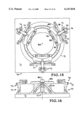
- FIG. 1 illustrates an embodiment of a projection optics (PO) box or assembly containing a plurality of optics and mode in accordance with the present invention.
- PO projection optics
- FIG. 2 is an isometric view of the FIG. 1 PO box composed of bulkheads with cutouts to provide access to the optics therein.
- FIG. 3 illustrates the optical path of the projected beam of the FIG. 1 PO box, positioned between a mask and target (wafer) of an EUVL system.
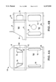
- FIG. 4A shows a front view of the PO box of FIG. 1.
- FIG. 4B shows a side view of the PO box of FIG. 1.
- FIG. 5 illustrates a cross section of the PO box of FIG. 1.
- FIG. 6 illustrates a cross section of the PO box of FIG. 1 with the optics path therethrough between a mask and a target.
- FIG. 7 is a view taken in the direction of arrows 7--7 of FIG. 6.
- FIG. 8 is a section of the PO box taken in the direction of arrows 8--8 of FIG. 6.
- FIG. 9 is a top view of an optics assembly taken in the direction of arrows 9--9 of FIG. 6.
- FIG. 10 is a view looking down on an optics assembly in the direction of arrows 10--10 of FIG. 6.
- FIG. 11 is a view looking up at an optics assembly in the direction of arrows 11--11 of FIG. 6.
- FIG. 12 is a view looking down on the backside of an optics assembly in the direction of arrows 12--12 of FIG. 6.
- FIG. 13 is a view of an EUVL system with the PO box of the present invention positioned in the projection chamber of the system.
- FIG. 14 illustrates the optical path of the EUVL system of FIG. 13.
- FIGS. 15 and 16 are top and side views of an embodiment of a precision actuator that may be utilized for positioning the optics of the PO box of FIG. 1.
- the present invention is directed to a projection optics (PO) box or assembly for use in an imaging system, such as an EUVL system using 10 to 14 nm wavelength soft x-ray photon, wherein high-reflectivity (65% or greater) of each optical component is essential.
- the PO box is composed of a plurality of bulkheads having opening therein to provide access to the optics within the PO box, and each optic may be mounted on a precision actuator to enable movement in the x, y, and z planes which provides exact constraint.
- the embodiment of the invention illustrated and described hereinafter is constructed for use intermediate the mask and target of an EUVL system, but the invention may be utilized in other imaging systems. In this embodiment a four (4) optic or mirror arrangement is utilized with each optic or mirror mounted to a precision actuator. However, any number of optics may be utilized, and any or all of the optics may be mounted via a precision actuator.
- FIG. 1 illustrates an embodiment of the PO box or assembly and is generally indicated at 10 having a structure defining a housing 2 having four (4) precision actuator assemblies 4 mounted in or on housing 2 for optics or mirrors M1, M2, M3 and M4, as shown in FIG. 3.
- FIG. 2 shows an isometric view of the PO box structure or housing 2 composed of a top bulkhead 6 having an opening 8 for a precision actuator, a middle bulkhead 12 having a cutout 14 for precision actuator, and a bottom bulkhead 16 having a cutout for a precision actuator.
- the bulkheads 6, 12 and 16 are interconnected by wall members 30.
- An attachment point for the fourth precision actuator is indicated at 20.
- the bulkheads 6, 12 and 16 and the wall members 30 are welded together to form a unit construction of maximum rigidity.
- FIG. 3 shows the optics path of a projected or illuminating beam 22 from a source (see FIG. 14, for example) which illuminates a mask/reticle 24 which forms a pattern beam 26 and travels to mirror M1, which reflects beam 26 onto mirror M2, and is again reflected onto mirror M3, which in turn reflects the pattern beam 26 onto a target 28, such as a silicon wafer.
- the PO box 10 provides a multipass, or folded, reduction system having an offset optical axis indicated at 34.
- the composition and dimensions of each of mirrors M1, M2, M3, and M4 is dependent on the specific application, wavelength, etc. By way of example, the distance from mask 24 to wafer 28 is 1.1 m.
- each of mirrors M1 to M4 are mounted on a precision actuator indicated at 4 in FIG. 1, which may be of the type illustrated in FIGS. 15-16 and described hereinafter.
- FIG. 4A and 4B show front and side views of the PO box 10 of FIG. 1 illustrating the top, middle, and bottom bulkheads 6, 12 and 16, and the interconnecting wall members 30.
- the wall members 30 are provided with a plurality of access openings generally indicated at 31.
- FIG. 5 shows a cross-section of the housing or structure 2 of the PO box 10 of FIG. 1 with the cutouts 8, 14 and 18 in bulkheads 6, 12 and 16 for mounting the precision actuators 4 (see FIG. 1).
- the wall members 30 are welded to the bulkheads 6, 12 and 16 as indicated at 32 to provide the rigid unit structure 2.
- FIG. 6 is a cross section of the PO box or assembly 10 illustrating the four (4) precision actuators 4 on which are mounted the optics or mirrors M1, M2, M3, and M4 with the optical paths or beam 22 and 26 as illustrated in FIG. 3 and described above.
- the illuminating beam 22 from a source illuminates mask/reticle 24 and a reflected pattern from 24 now defining a pattern beam 26 travels via mirrors M1 to M4 onto the target 28, with the optical path through the PO box 10 being defined as a multipass (folded) reduction system.
- the precision actuator 4 may be of the type illustrated and described thereinafter with respect to FIGS. 15 and 16, and may be constructed as described and claimed in above-referenced copending application Ser. No. 09/098,693.
- FIG. 7 is a view taken in the direction of arrows 7--7 of FIG. 6 looking up at the bottom of bulkhead 16 and shows the cutout 18 in bulkhead 16 and the precision actuator 4 as well as the bottom of mirror M1. Also shown is mirror M3 from its bottom side and the precision actuator 4 therefor. Additional cutouts 36 and 38 are provided in bulkhead 16 and precision actuator 4 for mirror M3.
- Mirror M3 is shown as shaped to pass pattern beam 26 onto mirror M4 and back through cutout 38 to target 28, as seen in FIG. 6.
- FIG. 8 shows a section of PO box or assembly 10 taken in the direction of arrows 8--8 of FIG. 6, and shows middle bulkhead 12 with cutout 14 and precision actuator 4 with a view of mirror M2 contoured to allow passage of pattern beam 26 through precision actuator 4 onto mirror M1, with the beam 26 being reflection from mirror M1 to mirror M2 onto mirror M3.
- FIG. 9 is a view taken in the direction of arrow 9--9 of FIG. 6 and is a top view of bulkhead 6 with cutout 8, precision actuator 4, and the backside of mirror M2. Also shown is a section of middle bulkhead 12, cutout 14, precision actuator 4, and mirror M4, showing the backside of mirror M4. As seen in FIG. 6, the pattern beam 26 passes through an opening in precision actuator 4 of mirror M2 onto mirror M2 and which is then reflected onto mirror M2.
- FIG. 10 is a view taken in the direction of arrows 10--10 of FIG. 6 looking down on the reflective or front surface of mirror M3, and showing the bottom bulkhead 16, cutout 18, and precision actuator 4 for mirror M3.
- the pattern beam 26 passes from mirror M3 to mirror M4 and through cutout 38 in precision actuator 4 and cutout 36 in bottom bulkhead 16 to target 28.
- Also shown mounted in bulkhead 16 is the precision actuator 4 for mirror M1 and the reflective or front surface of mirror M1.
- FIG. 11 is a view looking up at mirror M4 in the direction of arrows 11--11 of FIG. 6 and shows the reflective or front surface of mirror M4 mounted in precision actuator 4 located in cutout 14 of middle bulkhead 12. Also shown in the reflective or front surface of mirror M2 mounted in its precision actuator 4.
- FIG. 12 is a view looking down on the backside of mirror M4 inm the direction of arrows 12--12 of FIG. 6, and shows middle bulkhead 12, cutout 14, and precision actuator 4 for mirror M4. Also shown is the reflective or front surface of mirror M1 and a portion of precision actuator 4 for mirror M3.
- FIGS. 13 and 14 schematically illustrate an embodiment of an EUVL system and the optical path thereof, with the PO box or assembly of the present invention mounted therein.
- the system includes a source chamber 50 and a main vacuum or projection chamber 51 provided with appropriate connector tube indicated at 52, with projection chamber 51 being mounted on a support 53, and source chamber 50 being provided with a reflector box 54 via a tube 55, with reflector box 54 being connected to a source, such as a laser, via a tube 56.
- the housing or structure 2 of PO box or assembly 10 is mounted in projection chamber 51.
- the reason for the projection chamber 51 in this embodiment being mounted on support 53 is apparent from FIG. 14 to enable the illumination beam 22 to be directed onto the mask/reticle 24.
- FIG. 14 is apparent from FIG. 14 to enable the illumination beam 22 to be directed onto the mask/reticle 24.
- a laser beam 57 passes through tube 56 onto a reflector 58 located in reflector box 54 and through tube 55 into source chamber 50 in which is mounted a collector 59, a plasma generator 60 having a gas inlet or supply 61, and a reflector assembly 62.
- the laser beam 57 after passing through the collector 59 and plasma generator 60 results in the illumination beam 22.
- the beam 22 from reflector assembly 62 passes through connector tube 52 into the main or projection chamber 51 and is reflected by an optic or mirror 63 onto the mask/reticle 24, which became the pattern beam 26 as described above.
- the EUVL system is provided with an appropriate vacuum system, electrical system, and precision actuator control system, etc., to enable operation of the overall EUVL system.
- FIGS. 15 and 16 show top and side views of an embodiment of a precision actuator, such as actuators 4 of the FIG. 1 PO box 10.
- the actuator, generally indicated at 70 provides three degrees of freedom, known in the art as tip, tilt, and piston (the x, y and z axis), and belongs to the class of parallel-link mechanisms, which offer significant advantages at the complication of coordinated axis moves. Besides being stiffer, parallel-link mechanisms provide exact constraint for the suspended optical surface, such as mirrors M1 to M4 of PO box 10.
- the precision actuator 70 includes a base or support plate 71 having an opening 72, with three commercially available push-pull (linear) actuators 73 equally positioned around opening 72.
- Each linear actuator 73 is secured to base plate 71 and includes an actuator adjustment knob 74, an adjustment screw 75, and a spring plunger mount 76.
- the actuator 70 includes three equally spaced flexure mechanisms 77 pressed against a spring plunger 76 of each linear actuator 73.
- Each of the spaced flexure mechanisms include a first flexure 78, a second flexure 79, a stiffening ring 80, a flexure link plate 81, and a mounting boss 82 which connects the second flexure 79 to an optical mount 83 mounted on ring 30 having a vertical axis (z) indicated at 84. Since the details of the precision actuator 70 of FIGS. 15 and 16 do not constitute part of the present invention, further description is deemed unnecessary. However, such details are set forth in above-referenced copending application Ser. No. 09/098,693.
- the present invention provides a projection optics box or assembly which includes a plurality of optics or mirrors, each of which may be mounted via a precision actuator to provide movement in the x, y, and z planes.
- the optic path within the housing is a multipass (folder) reduction system, and this is particularly adapted for use in an EUVL system operating in the 10-14 nm region wavelength.
Abstract
Description
Claims (19)
Priority Applications (3)
| Application Number | Priority Date | Filing Date | Title |
|---|---|---|---|
| US09/217,739 US6147818A (en) | 1998-12-21 | 1998-12-21 | Projection optics box |
| AU20504/00A AU2050400A (en) | 1998-12-21 | 1999-12-10 | Projection optics box or assembly |
| PCT/US1999/029396 WO2000038017A1 (en) | 1998-12-21 | 1999-12-10 | Projection optics box or assembly |
Applications Claiming Priority (1)
| Application Number | Priority Date | Filing Date | Title |
|---|---|---|---|
| US09/217,739 US6147818A (en) | 1998-12-21 | 1998-12-21 | Projection optics box |
Publications (1)
| Publication Number | Publication Date |
|---|---|
| US6147818A true US6147818A (en) | 2000-11-14 |
Family
ID=22812315
Family Applications (1)
| Application Number | Title | Priority Date | Filing Date |
|---|---|---|---|
| US09/217,739 Expired - Lifetime US6147818A (en) | 1998-12-21 | 1998-12-21 | Projection optics box |
Country Status (3)
| Country | Link |
|---|---|
| US (1) | US6147818A (en) |
| AU (1) | AU2050400A (en) |
| WO (1) | WO2000038017A1 (en) |
Cited By (28)
| Publication number | Priority date | Publication date | Assignee | Title |
|---|---|---|---|---|
| EP1310829A1 (en) * | 2001-11-07 | 2003-05-14 | ASML Netherlands B.V. | Lithographic apparatus and device manufacturing method |
| US20030090641A1 (en) * | 2001-11-07 | 2003-05-15 | Asml Netherlands, B.V. | Lithographic apparatus and device manufacturing method |
| US6642995B2 (en) | 2001-11-07 | 2003-11-04 | Euv Llc | Mask-to-wafer alignment system |
| US20030235682A1 (en) * | 2002-06-21 | 2003-12-25 | Sogard Michael R. | Method and device for controlling thermal distortion in elements of a lithography system |
| EP1526407A2 (en) * | 2003-10-21 | 2005-04-27 | ASML Netherlands B.V. | An assembly, a lithographic apparatus, and a device manufacturing method |
| US20050099069A1 (en) * | 2003-11-06 | 2005-05-12 | Koorneef Lucas F. | Hermetically sealed elements of an actuator |
| US20050157383A1 (en) * | 2004-01-16 | 2005-07-21 | Tichenor Daniel A. | Condenser optic with sacrificial reflective surface |
| US20050168842A1 (en) * | 2004-01-29 | 2005-08-04 | Michael Long | Two axis tip-tilt platform |
| WO2005083487A1 (en) * | 2004-02-26 | 2005-09-09 | Carl Zeiss Smt Ag | Housing structure |
| US20050213069A1 (en) * | 2002-10-25 | 2005-09-29 | Nikon Corporation | Extreme ultraviolet exposure apparatus and vacuum chamber |
| US20050237640A1 (en) * | 2004-04-21 | 2005-10-27 | Cipra Dale O | Laser beam jitter reduction device on a laser optical bench |
| US20060012893A1 (en) * | 2002-10-08 | 2006-01-19 | Ulrich Weber | Objective, in particular a projection objective in microlithography |
| US20060158046A1 (en) * | 2005-01-18 | 2006-07-20 | Barnes Ted W | Light direction assembly shorted turn |
| US20070284502A1 (en) * | 2006-06-13 | 2007-12-13 | Nikon Corporation | Hexapod kinematic mountings for optical elements, and optical systems comprising same |
| US20080291416A1 (en) * | 2006-01-30 | 2008-11-27 | Jin Nishikawa | Optical member-holding apparatus, method for adjusting position of optical member, and exposure apparatus |
| DE102008054581A1 (en) | 2008-02-29 | 2009-09-03 | Carl Zeiss Smt Ag | Projection system for projection exposure system for manufacturing micro-and/or nanostructure semiconductor components, has carrier structure provided for supporting projection lens in floor and implemented for holding projection lens |
| US20120044471A1 (en) * | 2009-04-27 | 2012-02-23 | Asml Netherlands B.V. | Lithographic Apparatus and Method |
| US20140131587A1 (en) * | 2009-04-23 | 2014-05-15 | Gigaphoton Inc. | Extreme ultraviolet light source apparatus |
| US9091843B1 (en) | 2014-03-16 | 2015-07-28 | Hyperion Development, LLC | Optical assembly for a wide field of view point action camera with low track length to focal length ratio |
| US9316820B1 (en) | 2014-03-16 | 2016-04-19 | Hyperion Development, LLC | Optical assembly for a wide field of view point action camera with low astigmatism |
| US9316808B1 (en) | 2014-03-16 | 2016-04-19 | Hyperion Development, LLC | Optical assembly for a wide field of view point action camera with a low sag aspheric lens element |
| US9494772B1 (en) | 2014-03-16 | 2016-11-15 | Hyperion Development, LLC | Optical assembly for a wide field of view point action camera with low field curvature |
| US9726859B1 (en) | 2014-03-16 | 2017-08-08 | Navitar Industries, Llc | Optical assembly for a wide field of view camera with low TV distortion |
| US9835835B1 (en) | 2015-04-10 | 2017-12-05 | Navitar Industries, Llc | Projection zoom lens and camera |
| US9995910B1 (en) | 2014-03-16 | 2018-06-12 | Navitar Industries, Llc | Optical assembly for a compact wide field of view digital camera with high MTF |
| US10139595B1 (en) | 2014-03-16 | 2018-11-27 | Navitar Industries, Llc | Optical assembly for a compact wide field of view digital camera with low first lens diameter to image diagonal ratio |
| US10386604B1 (en) | 2014-03-16 | 2019-08-20 | Navitar Industries, Llc | Compact wide field of view digital camera with stray light impact suppression |
| US10545314B1 (en) | 2014-03-16 | 2020-01-28 | Navitar Industries, Llc | Optical assembly for a compact wide field of view digital camera with low lateral chromatic aberration |
Citations (7)
| Publication number | Priority date | Publication date | Assignee | Title |
|---|---|---|---|---|
| US5410434A (en) * | 1993-09-09 | 1995-04-25 | Ultratech Stepper, Inc. | Reflective projection system comprising four spherical mirrors |
| US5420436A (en) * | 1992-11-27 | 1995-05-30 | Hitachi, Ltd. | Methods for measuring optical system, and method and apparatus for exposure using said measuring method |
| US5526192A (en) * | 1993-03-30 | 1996-06-11 | Nikon Corporation | Vibration prevention device for an optical system |
| US5581317A (en) * | 1993-07-13 | 1996-12-03 | Nikon Corporation | Vibration preventing device |
| US5592239A (en) * | 1993-07-14 | 1997-01-07 | Sony Corporation | Projector device |
| JPH10293676A (en) * | 1997-04-18 | 1998-11-04 | Fuji Xerox Co Ltd | Icon display control device and method |
| US5959784A (en) * | 1996-04-24 | 1999-09-28 | Nikon Corporation | Optical projection systems and projection-exposure apparatus comprising same |
Family Cites Families (6)
| Publication number | Priority date | Publication date | Assignee | Title |
|---|---|---|---|---|
| US4664487A (en) * | 1985-09-30 | 1987-05-12 | Rockwell International Corporation | Laser mirror positioning apparatus |
| EP0947882B1 (en) * | 1986-07-11 | 2006-03-29 | Canon Kabushiki Kaisha | X-ray reduction projection exposure system of reflection type |
| US5063586A (en) * | 1989-10-13 | 1991-11-05 | At&T Bell Laboratories | Apparatus for semiconductor lithography |
| US5626424A (en) * | 1994-07-21 | 1997-05-06 | Raytek Subsidiary, Inc. | Dual light source aiming mechanism and improved actuation system for hand-held temperature measuring unit |
| US5805365A (en) * | 1995-10-12 | 1998-09-08 | Sandia Corporation | Ringfield lithographic camera |
| US5640283A (en) * | 1995-10-20 | 1997-06-17 | The Aerospace Corporation | Wide field, long focal length, four mirror telescope |
-
1998
- 1998-12-21 US US09/217,739 patent/US6147818A/en not_active Expired - Lifetime
-
1999
- 1999-12-10 AU AU20504/00A patent/AU2050400A/en not_active Abandoned
- 1999-12-10 WO PCT/US1999/029396 patent/WO2000038017A1/en active Application Filing
Patent Citations (7)
| Publication number | Priority date | Publication date | Assignee | Title |
|---|---|---|---|---|
| US5420436A (en) * | 1992-11-27 | 1995-05-30 | Hitachi, Ltd. | Methods for measuring optical system, and method and apparatus for exposure using said measuring method |
| US5526192A (en) * | 1993-03-30 | 1996-06-11 | Nikon Corporation | Vibration prevention device for an optical system |
| US5581317A (en) * | 1993-07-13 | 1996-12-03 | Nikon Corporation | Vibration preventing device |
| US5592239A (en) * | 1993-07-14 | 1997-01-07 | Sony Corporation | Projector device |
| US5410434A (en) * | 1993-09-09 | 1995-04-25 | Ultratech Stepper, Inc. | Reflective projection system comprising four spherical mirrors |
| US5959784A (en) * | 1996-04-24 | 1999-09-28 | Nikon Corporation | Optical projection systems and projection-exposure apparatus comprising same |
| JPH10293676A (en) * | 1997-04-18 | 1998-11-04 | Fuji Xerox Co Ltd | Icon display control device and method |
Cited By (58)
| Publication number | Priority date | Publication date | Assignee | Title |
|---|---|---|---|---|
| US20030090641A1 (en) * | 2001-11-07 | 2003-05-15 | Asml Netherlands, B.V. | Lithographic apparatus and device manufacturing method |
| US6642995B2 (en) | 2001-11-07 | 2003-11-04 | Euv Llc | Mask-to-wafer alignment system |
| US6734949B2 (en) | 2001-11-07 | 2004-05-11 | Asml Netherlands B.V. | Lithographic apparatus and device manufacturing method |
| EP1310829A1 (en) * | 2001-11-07 | 2003-05-14 | ASML Netherlands B.V. | Lithographic apparatus and device manufacturing method |
| KR100767833B1 (en) * | 2001-11-07 | 2007-10-17 | 에이에스엠엘 네델란즈 비.브이. | Lithographic Apparatus and Device Manufacturing Method |
| US20030235682A1 (en) * | 2002-06-21 | 2003-12-25 | Sogard Michael R. | Method and device for controlling thermal distortion in elements of a lithography system |
| US20060012893A1 (en) * | 2002-10-08 | 2006-01-19 | Ulrich Weber | Objective, in particular a projection objective in microlithography |
| US20050213069A1 (en) * | 2002-10-25 | 2005-09-29 | Nikon Corporation | Extreme ultraviolet exposure apparatus and vacuum chamber |
| US7417708B2 (en) | 2002-10-25 | 2008-08-26 | Nikon Corporation | Extreme ultraviolet exposure apparatus and vacuum chamber |
| CN100461001C (en) * | 2003-10-21 | 2009-02-11 | Asml荷兰有限公司 | An assembly, a lithographic apparatus, and a device manufacturing method |
| US7474378B2 (en) | 2003-10-21 | 2009-01-06 | Asml Netherlands B.V. | Assembly, a lithographic apparatus, and a device manufacturing method |
| US7525637B2 (en) | 2003-10-21 | 2009-04-28 | Asml Netherlands B.V. | Assembly |
| EP1526407A3 (en) * | 2003-10-21 | 2009-04-22 | ASML Netherlands B.V. | An assembly, a lithographic apparatus, and a device manufacturing method |
| EP1526407A2 (en) * | 2003-10-21 | 2005-04-27 | ASML Netherlands B.V. | An assembly, a lithographic apparatus, and a device manufacturing method |
| US20080158534A1 (en) * | 2003-10-21 | 2008-07-03 | Asml Netherlands B.V. | Assembly |
| US20050099069A1 (en) * | 2003-11-06 | 2005-05-12 | Koorneef Lucas F. | Hermetically sealed elements of an actuator |
| US7183674B2 (en) * | 2003-11-06 | 2007-02-27 | Carl Zeiss Smt Ag | Hermetically sealed elements of an actuator |
| US20050157383A1 (en) * | 2004-01-16 | 2005-07-21 | Tichenor Daniel A. | Condenser optic with sacrificial reflective surface |
| US7081992B2 (en) | 2004-01-16 | 2006-07-25 | Euv Llc | Condenser optic with sacrificial reflective surface |
| US6972913B2 (en) | 2004-01-29 | 2005-12-06 | Hewlett-Packard Development Company, L.P. | Two axis tip-tilt platform |
| US20050168842A1 (en) * | 2004-01-29 | 2005-08-04 | Michael Long | Two axis tip-tilt platform |
| US20110216428A1 (en) * | 2004-02-26 | 2011-09-08 | Carl Zeiss Smt Gmbh | Housing structure |
| US20090303626A1 (en) * | 2004-02-26 | 2009-12-10 | Carl Zeiss Smt Ag | Housing structure |
| JP2007524129A (en) * | 2004-02-26 | 2007-08-23 | カール・ツァイス・エスエムティー・アーゲー | Housing structure |
| US8018664B2 (en) | 2004-02-26 | 2011-09-13 | Carl Zeiss Smt Gmbh | Housing structure |
| JP2012048251A (en) * | 2004-02-26 | 2012-03-08 | Carl Zeiss Smt Gmbh | Housing structure |
| WO2005083487A1 (en) * | 2004-02-26 | 2005-09-09 | Carl Zeiss Smt Ag | Housing structure |
| US7064908B2 (en) * | 2004-04-21 | 2006-06-20 | The Boeing Company | Laser beam jitter reduction device on a laser optical bench |
| US20050237640A1 (en) * | 2004-04-21 | 2005-10-27 | Cipra Dale O | Laser beam jitter reduction device on a laser optical bench |
| US7279812B2 (en) | 2005-01-18 | 2007-10-09 | Hewlett-Packard Development Company, L.P. | Light direction assembly shorted turn |
| US20060158046A1 (en) * | 2005-01-18 | 2006-07-20 | Barnes Ted W | Light direction assembly shorted turn |
| US8576375B2 (en) * | 2006-01-30 | 2013-11-05 | Nikon Corporation | Optical member-holding apparatus, method for adjusting position of optical member, and exposure apparatus |
| US20080291416A1 (en) * | 2006-01-30 | 2008-11-27 | Jin Nishikawa | Optical member-holding apparatus, method for adjusting position of optical member, and exposure apparatus |
| US20070284502A1 (en) * | 2006-06-13 | 2007-12-13 | Nikon Corporation | Hexapod kinematic mountings for optical elements, and optical systems comprising same |
| DE102008054581A1 (en) | 2008-02-29 | 2009-09-03 | Carl Zeiss Smt Ag | Projection system for projection exposure system for manufacturing micro-and/or nanostructure semiconductor components, has carrier structure provided for supporting projection lens in floor and implemented for holding projection lens |
| US9179534B2 (en) * | 2009-04-23 | 2015-11-03 | Gigaphoton Inc. | Extreme ultraviolet light source apparatus |
| US20140131587A1 (en) * | 2009-04-23 | 2014-05-15 | Gigaphoton Inc. | Extreme ultraviolet light source apparatus |
| US20120044471A1 (en) * | 2009-04-27 | 2012-02-23 | Asml Netherlands B.V. | Lithographic Apparatus and Method |
| US9726859B1 (en) | 2014-03-16 | 2017-08-08 | Navitar Industries, Llc | Optical assembly for a wide field of view camera with low TV distortion |
| US10107989B1 (en) | 2014-03-16 | 2018-10-23 | Navitar Industries, Llc | Optical assembly for a wide field of view point action camera with low field curvature |
| US9316808B1 (en) | 2014-03-16 | 2016-04-19 | Hyperion Development, LLC | Optical assembly for a wide field of view point action camera with a low sag aspheric lens element |
| US9494772B1 (en) | 2014-03-16 | 2016-11-15 | Hyperion Development, LLC | Optical assembly for a wide field of view point action camera with low field curvature |
| US9091843B1 (en) | 2014-03-16 | 2015-07-28 | Hyperion Development, LLC | Optical assembly for a wide field of view point action camera with low track length to focal length ratio |
| US9778444B1 (en) | 2014-03-16 | 2017-10-03 | Navitar Industries, Llc | Optical assembly for a wide field of view point action camera with low astigmatism |
| US9784943B1 (en) | 2014-03-16 | 2017-10-10 | Navitar Industries, Llc | Optical assembly for a wide field of view point action camera with a low sag aspheric lens element |
| US11754809B2 (en) | 2014-03-16 | 2023-09-12 | Navitar, Inc. | Optical assembly for a wide field of view point action camera with low field curvature |
| US9995910B1 (en) | 2014-03-16 | 2018-06-12 | Navitar Industries, Llc | Optical assembly for a compact wide field of view digital camera with high MTF |
| US9316820B1 (en) | 2014-03-16 | 2016-04-19 | Hyperion Development, LLC | Optical assembly for a wide field of view point action camera with low astigmatism |
| US10139595B1 (en) | 2014-03-16 | 2018-11-27 | Navitar Industries, Llc | Optical assembly for a compact wide field of view digital camera with low first lens diameter to image diagonal ratio |
| US10139599B1 (en) | 2014-03-16 | 2018-11-27 | Navitar Industries, Llc | Optical assembly for a wide field of view camera with low TV distortion |
| US10317652B1 (en) | 2014-03-16 | 2019-06-11 | Navitar Industries, Llc | Optical assembly for a wide field of view point action camera with low astigmatism |
| US10746967B2 (en) | 2014-03-16 | 2020-08-18 | Navitar Industries, Llc | Optical assembly for a wide field of view point action camera with low field curvature |
| US10386604B1 (en) | 2014-03-16 | 2019-08-20 | Navitar Industries, Llc | Compact wide field of view digital camera with stray light impact suppression |
| US10545314B1 (en) | 2014-03-16 | 2020-01-28 | Navitar Industries, Llc | Optical assembly for a compact wide field of view digital camera with low lateral chromatic aberration |
| US10545313B1 (en) | 2014-03-16 | 2020-01-28 | Navitar Industries, Llc | Optical assembly for a wide field of view point action camera with a low sag aspheric lens element |
| US10739561B1 (en) | 2014-03-16 | 2020-08-11 | Navitar Industries, Llc | Optical assembly for a compact wide field of view digital camera with high MTF |
| US10330900B1 (en) | 2015-04-10 | 2019-06-25 | Navitar Industries, Llc | Projection zoom lens and camera |
| US9835835B1 (en) | 2015-04-10 | 2017-12-05 | Navitar Industries, Llc | Projection zoom lens and camera |
Also Published As
| Publication number | Publication date |
|---|---|
| WO2000038017A1 (en) | 2000-06-29 |
| AU2050400A (en) | 2000-07-12 |
Similar Documents
| Publication | Publication Date | Title |
|---|---|---|
| US6147818A (en) | Projection optics box | |
| US6031598A (en) | Extreme ultraviolet lithography machine | |
| US4242588A (en) | X-ray lithography system having collimating optics | |
| US7088424B2 (en) | Lithographic projection apparatus, reflector assembly for use therein, and device manufacturing method | |
| US5900637A (en) | Maskless lithography using a multiplexed array of fresnel zone plates | |
| US7203275B2 (en) | Multilayer film reflector and X-ray exposure system | |
| US6522716B1 (en) | Multilayer-film reflective mirrors, extreme UV microlithography apparatus comprising same, and microelectronic-device manufacturing methods utilizing same | |
| JP5475756B2 (en) | Method for forming a spectral purity filter | |
| KR101470769B1 (en) | Illumination system of a microlithographic projection exposure apparatus | |
| JP4313328B2 (en) | Lithographic apparatus, device manufacturing method and variable attenuator | |
| EP1319988B1 (en) | High luminosity source for EUV lithography | |
| US20060175556A1 (en) | Illumination optical system, exposure apparatus, and device manufacturing method | |
| US20060245540A1 (en) | Illumination system particularly for microlithography | |
| KR100737645B1 (en) | Dual hemispherical collectors | |
| JP4981858B2 (en) | Actuator system using multiple piezoelectric actuators | |
| JP2002514007A (en) | Irradiation mechanism especially used for EUV (extreme ultraviolet) lithography | |
| KR20050007150A (en) | Mirror and lithographic apparatus with mirror | |
| US20070159611A1 (en) | Source Multiplexing in Lithography | |
| CN100470368C (en) | Lithographic projection apparatus with lollector including concave mirror and convex mirror | |
| KR20010006764A (en) | Illumination system for extreme ultraviolet radiation and its application in lithographic projection apparatus | |
| US9285690B2 (en) | Mirror, lithographic apparatus and device manufacturing method | |
| US7309869B2 (en) | Lithographic apparatus, device manufacturing method and radiation system | |
| Kinoshita et al. | Three-aspherical-mirror system for EUV lithography | |
| US6859263B2 (en) | Apparatus for generating partially coherent radiation | |
| US10928733B2 (en) | Illumination optic for projection lithography |
Legal Events
| Date | Code | Title | Description |
|---|---|---|---|
| AS | Assignment |
Owner name: CALIFORNIA, REGENTS OF THE UNIVERSITY OF, THE, CAL Free format text: ASSIGNMENT OF ASSIGNORS INTEREST;ASSIGNORS:HALE, LAYTON C.;MALSBURY, TERRY;HUDYMA, RUSSELL M.;AND OTHERS;REEL/FRAME:009672/0138 Effective date: 19981217 Owner name: REGENTS OF THE UNIVERSITY OF CALIFORNIA, THE, CALI Free format text: ASSIGNMENT OF ASSIGNORS INTEREST;ASSIGNORS:HALE, LAYTON C.;MALSBURY, TERRY;HUDYMA, RUSSELL M.;AND OTHERS;REEL/FRAME:009672/0138 Effective date: 19981217 |
|
| AS | Assignment |
Owner name: ENERGY, U.S. DEPARTMENT OF, CALIFORNIA Free format text: CONFIRMATORY LICENSE;ASSIGNOR:CALIFORNIA, UNIVERSITY OF;REEL/FRAME:010611/0852 Effective date: 19990813 |
|
| STCF | Information on status: patent grant |
Free format text: PATENTED CASE |
|
| AS | Assignment |
Owner name: EUV LIMITED LIABILITY COMPANY, CALIFORNIA Free format text: ASSIGNMENT OF ASSIGNORS INTEREST;ASSIGNOR:REGENTS OF THE UNIVERSITY OF CALIFORNIA, THE;REEL/FRAME:012287/0936 Effective date: 20010619 |
|
| FPAY | Fee payment |
Year of fee payment: 4 |
|
| FEPP | Fee payment procedure |
Free format text: PAYOR NUMBER ASSIGNED (ORIGINAL EVENT CODE: ASPN); ENTITY STATUS OF PATENT OWNER: LARGE ENTITY |
|
| FPAY | Fee payment |
Year of fee payment: 8 |
|
| FPAY | Fee payment |
Year of fee payment: 12 |