US6147634A - Method and apparatus for digital to analog conversion with reduced noise - Google Patents
Method and apparatus for digital to analog conversion with reduced noise Download PDFInfo
- Publication number
- US6147634A US6147634A US09/211,616 US21161698A US6147634A US 6147634 A US6147634 A US 6147634A US 21161698 A US21161698 A US 21161698A US 6147634 A US6147634 A US 6147634A
- Authority
- US
- United States
- Prior art keywords
- digital
- signal
- analog
- signals
- produce
- Prior art date
- Legal status (The legal status is an assumption and is not a legal conclusion. Google has not performed a legal analysis and makes no representation as to the accuracy of the status listed.)
- Expired - Lifetime
Links
Images
Classifications
-
- H—ELECTRICITY
- H03—ELECTRONIC CIRCUITRY
- H03M—CODING; DECODING; CODE CONVERSION IN GENERAL
- H03M3/00—Conversion of analogue values to or from differential modulation
- H03M3/30—Delta-sigma modulation
- H03M3/322—Continuously compensating for, or preventing, undesired influence of physical parameters
- H03M3/324—Continuously compensating for, or preventing, undesired influence of physical parameters characterised by means or methods for compensating or preventing more than one type of error at a time, e.g. by synchronisation or using a ratiometric arrangement
- H03M3/344—Continuously compensating for, or preventing, undesired influence of physical parameters characterised by means or methods for compensating or preventing more than one type of error at a time, e.g. by synchronisation or using a ratiometric arrangement by filtering other than the noise-shaping inherent to delta-sigma modulators, e.g. anti-aliasing
-
- H—ELECTRICITY
- H03—ELECTRONIC CIRCUITRY
- H03M—CODING; DECODING; CODE CONVERSION IN GENERAL
- H03M3/00—Conversion of analogue values to or from differential modulation
- H03M3/30—Delta-sigma modulation
- H03M3/50—Digital/analogue converters using delta-sigma modulation as an intermediate step
Definitions
- This invention relates generally to digital to analog signal conversions and more particularly to reducing noise within digital to analog converters and applications thereof.
- conversion of analog to digital signals and digital to analog signals is known. Conversion of analog to digital signals may be done utilizing Sigma Delta Modulators, successive approximations and/or flash circuits. The conversion of digital signals to analog signals may be done using complimentary circuitry to Sigma Delta Modulators, successive approximation circuits, and/or flash circuits.
- a Sigma Delta analog to digital converter includes a first or second order Sigma Delta Modulator and a quantizer.
- a first order Sigma Delta Modulator includes a single modulation stage while a second order Sigma Delta Modulator includes two modulation stages.
- the output of the quantizer is fed back to each stage of the said Sigma Delta Modulator via digital to analog converter modules.
- ⁇ ADC provide a relatively high-speed analog to digital conversion there are some limitations for high fidelity applications. For instance, when the analog signal is a DC value for a relatively long time (much greater than the sampling rate), a noise component having a frequency of one-half the switching frequency is present. The noise can be injected into a voltage reference signal applied to the digital to analog converter feedback module and propagates through the ADC due to imperfections in the parts comprising the ADC. For example, amplifiers within the Sigma Delta ADC include offset that allow the noise to pass.
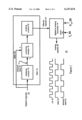
- FIG. 1 illustrates a schematic block diagram of a digital to analog converter in accordance with the present invention
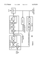
- FIG. 2 illustrates a schematic block diagram of a second order Sigma Delta Modulator in accordance with the present invention
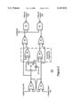
- FIG. 3 illustrates a schematic block diagram of the filter of FIGS. 1 and 2;
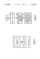
- FIG. 4 illustrates a schematic block diagram of an alternate digital to analog converter in accordance with the present invention.
- FIG. 5 illustrates a logic diagram of a method for converting digital to analog signals in accordance with the present invention.
- the present invention provides a method and apparatus for digital to analog signal conversions with reduced noise.
- processing begins by receiving a digital signal and filtering the digital signal to produce a filtered digital signal.
- the filtering is tuned to attenuate components of the digital signal having frequencies near one-half the sampling rate frequency and to pass other components of the digital signal having frequencies away from one-half the sampling rate frequency.
- the filtered signals are then converted to analog signals based on a clock signal having the sampling rate frequency and a voltage reference.
- the filter when the digital signal is substantially a square wave signal having a frequency of approximately one-half the sampling rate frequency, the filter attenuates noise produced near the one-half sampling rate frequency such that the resulting analog signal has a low noise component at one-half the sampling rate frequency.
- FIG. 1 illustrates a schematic block diagram of a digital to analog converter 10 that includes a filter 12 and a digital to analog converter module 14.
- the filter 12 includes a delaying module 16, a summing module 18, and a scaling module 20.
- the delaying module 16 is operably coupled to receive digital signals 22 and to produce therefrom delayed data 34.
- the delayed data is provided to the summing module 18 which also is operably coupled to receive the digital signals 22 as data signals 33.
- the summing module 18 adds the delayed data 34 to the data 32 to produce a resulting output which is provided to the scaling module 20.
- the scaling module 20 outputs filtered signals 24 to the digital to analog converter 14.
- the digital to analog converter 14 is operably coupled to a clock circuit F s 30 and a voltage reference 28.
- the data signals 32 and delayed data signals 34 are as shown in the timing diagram portion of FIG. 1.
- the delay data signals 34 and data signals 32 have a frequency of approximately one-half of the clock signal 30, i.e., the sampling frequency of the digital to analog converter 14.
- the delayed data 34 is delayed by a clock cycle with respect to data signals 32. With this type of delay, the delayed data signals 34 are substantially 180 degrees out of phase with respect to data signals 32.
- the output of the summing module 18 is substantially a zero output.
- the scaling module 20 produces the filtered signals 24, which are substantially zero.
- the analog signal is produced in part based on the clock signal 30 and the voltage reference 28. Note that due to practical limitations of the components used in analog to digital converters and also in Sigma Delta analog to digital converters, the voltage reference 28 may have noise imposed thereon that is substantially, or approximately, equal to one-half the sampling rate frequency. Without the filter 12, the digital signals 22 which are substantially equal to one-half the sample rate frequency when combined with the noise on the voltage reference 28 will produce an analog noise components of analog signal 26.
- filter 12 will pass, substantially unattenuated, the components having frequencies away from one-half the frequency sampling rate.
- filter 12 forms a notch filter that substantially attenuates components of the digital signal 22 near one-half the sampling rate and passes substantially unattenuated components having frequencies outside of the notched filter.
- digital signals, especially square wave signals are comprised of a plurality of sinusoidal components to produce the resulting square wave. As such, the sinusoidal signals that have frequency components near one-half the sampling rate frequency will be attenuated by filter 12.
- FIG. 2 illustrates a schematic block diagram of a Sigma Delta Analog to Digital Converter 40.
- the analog to digital converter 40 includes a first order stage 42, a second order stage 44, a quantizer 46, a second digital to analog converter feedback module 48 and the digital to analog converter 10 functioning as a first digital to analog converter feedback module.
- the first order stage 42 produces an integrated analog signal 68 of input analog signal 66.
- the first order stage 42 includes a first summing node 50 that subtracts an analog feedback signal 72 from the analog signal 66.
- the resulting signal is then provided to a constant module 52 that multiples the resultant signal by a constant.
- the resulting signal is provided to a second summing module 54 that sums the constant signal with a feedback signal of the integrated analog signal 68.
- the integrated analog signal 68 is produced by integrator 56.
- the second order stage 44 produces a second order integrated analog signal that is provided to quantizer 46.
- the second order stage includes a first summing module 58 that subtracts a second analog feedback signal 74 from the integrated analog signal 68.
- the resulting signal is provided to a constant module 60 and is subsequently provided to a second summing module 62.
- the second order stage 44 also includes an integrator 64 that produces a feedback signal, which is provided to the second summing module 62, and outputs the second order integrated analog signal.
- the quantizer 46 is operably coupled to receive the second order integrated analog signal and, based on the clock signal 30 which equals the sampling rate, produces the quantized digital signal 70.
- the quantized digital signal 70 is fed back through DAC 48 to produce the second analog feedback signal 74.
- the quantized digital signal 70 is fed back through DAC 10 to produce the analog feedback signal 72.
- the second order Sigma Delta Modulator of FIG. 2 may be a first order Sigma Delta Modulator by removing the second order stage 44 and the corresponding feedback DAC 48.
- the Sigma Delta Modulator may include a third or fourth quarter stage and corresponding feedback DACs to increase the order of the Sigma Delta Modulator.
- the DAC module 10 which was illustrated in the FIG. 1, is included only in the feedback path to the first order stage. This is in accordance with the preferred embodiment, however, the DAC module 10 may also be utilized in the feedback path to produce the second analog feedback signal 74.
- FIG. 3 illustrates a schematic block diagram of filter 12 for a differential filtering circuit.
- the digital input signals are received as a positive digital input 100 and a negative digital input 98 by a latch produced by NOR gates 80 and 82.
- the output of NOR gate 80 is provided to a D flip-flop 84 which functions as the delaying module 16.
- the output of NOR gate 82 is provided to the summing module 18 which includes a pair of exclusive OR gates 86 and 88.
- the exclusive OR gates 86 and 88 are operably coupled to receive the q and q complement outputs of the D flip-flop 84 and the output of the NOR gates 80 and 82 as shown.
- the filter 12 fully includes NOR gates 90 and 92 that are operably coupled to receive the outputs of exclusive OR gates 86 and 88 as shown and the outputs of NOR gates 80 and 82.
- the outputs of NOR gates 90 and 92 are provided to NAND gates 94 and 96.
- the other inputs of NAND gates 94 and 96 are coupled to an enabled and/or power down signal 102. When the enable and/or power down signal is low, the resulting filtered outputs 104 and 106 are produced. During a power down state or a non-enable state, the input to NAND gates 94 and 96 are high thereby disabling the outputs.
- FIG. 4 illustrates a schematic block diagram of a digital to analog conversion module 110 that includes a processing module 112 and memory 114.
- the processing module 112 may be a single processing entity or a plurality of processing entities.
- Such a processing entity may be a microprocessor, microcontroller, digital signal processor, microcomputer, central processing unit, state machine, logic circuitry, and/or any device that manipulates digital information based on operational instructions.
- the memory 114 may be a single memory device or a plurality of memory devices.
- Such a memory device may be read-only memory, floppy disk memory, random access memory, system memory, hard drive memory, external memory, magnetic tape memory, CD memory, and/or any device that stores digital information.
- the processing module includes logic circuitry and/or state machine to perform one or more of its functions
- the memory storing the corresponding operational instructions is embedded into the circuitry comprising the state machine and/or logic circuitry.
- the operational instructions performed by the processing module 112 and stored in memory 115 are described with reference to FIG. 5.
- FIG. 5 illustrates a logic diagram of a method for digital to analog conversion having low noise.
- the process begins at step 120 where a digital signal is received.
- the process then proceeds to step 122 where the digital signal is filtered at one-half the sampling frequency to produce a filtered digital signal.
- the filtering may be done by delaying the digital input signal to produce delay digital input signals.
- the delayed digital input signals are then summed with the digital input signals to produce a summed digital signals.
- the summed digital signals are then scaled to produce the digital signals.
- the process then proceeds to step 124 where the filtered digital signals are converted into analog signals based on a clock having a frequency of the sampling frequency and a voltage reference.
- Such digital to analog conversions may be implemented in Sigma Delta analog to digital converters in the feedback path.
- noise generated at one-half the sampling rate when the analog input is a DC value is substantially reduced, thereby enabling a low noise digital to analog converter to be produced as well as a low noise Sigma Delta analog to digital converter.
Abstract
Description
Claims (11)
Priority Applications (1)
| Application Number | Priority Date | Filing Date | Title |
|---|---|---|---|
| US09/211,616 US6147634A (en) | 1998-12-15 | 1998-12-15 | Method and apparatus for digital to analog conversion with reduced noise |
Applications Claiming Priority (1)
| Application Number | Priority Date | Filing Date | Title |
|---|---|---|---|
| US09/211,616 US6147634A (en) | 1998-12-15 | 1998-12-15 | Method and apparatus for digital to analog conversion with reduced noise |
Publications (1)
| Publication Number | Publication Date |
|---|---|
| US6147634A true US6147634A (en) | 2000-11-14 |
Family
ID=22787663
Family Applications (1)
| Application Number | Title | Priority Date | Filing Date |
|---|---|---|---|
| US09/211,616 Expired - Lifetime US6147634A (en) | 1998-12-15 | 1998-12-15 | Method and apparatus for digital to analog conversion with reduced noise |
Country Status (1)
| Country | Link |
|---|---|
| US (1) | US6147634A (en) |
Cited By (9)
| Publication number | Priority date | Publication date | Assignee | Title |
|---|---|---|---|---|
| US6292122B1 (en) * | 2000-03-04 | 2001-09-18 | Qualcomm, Incorporated | Digital-to-analog interface circuit having adjustable time response |
| WO2003052939A2 (en) * | 2001-12-18 | 2003-06-26 | Koninklijke Philips Electronics N.V. | Sigma delta a/d converter with firdac converter |
| US20040051654A1 (en) * | 2001-10-29 | 2004-03-18 | Kazunobu Ohkuri | D/A converter and output amplifying circuit |
| US20040140922A1 (en) * | 2003-01-21 | 2004-07-22 | Melanson John L. | Signal processing system with baseband noise modulation and noise filtering |
| US20040141562A1 (en) * | 2003-01-21 | 2004-07-22 | Plisch Marjorie R. | Signal processing system with baseband noise modulaltion chopper circuit timing to reduce noise |
| US20040216007A1 (en) * | 2003-03-28 | 2004-10-28 | Ess Technology, Inc. | System and method for compensating for error in a sigma delta circuit |
| US6954160B1 (en) * | 2004-04-09 | 2005-10-11 | Micrel, Inc. | Filter for digitally processing an analog input signal with analog feedback |
| EP2141814A1 (en) * | 2008-07-01 | 2010-01-06 | Telefonaktiebolaget LM Ericsson (publ) | Delta-sigma analog-to-digital converter, radio receiver, communication apparatus, method, and computer program |
| EP2157700A1 (en) * | 2008-08-19 | 2010-02-24 | Trident Microsystems (Far East) Ltd. | Delta-sigma analog-to-digital converter circuit and method for analog-to-digital converting |
Citations (5)
| Publication number | Priority date | Publication date | Assignee | Title |
|---|---|---|---|---|
| US5027120A (en) * | 1989-05-26 | 1991-06-25 | Gec-Marconi Limited | Delta-sigma converter with bandpass filter for noise reduction in receivers |
| US5349352A (en) * | 1992-12-21 | 1994-09-20 | Harris Corporation | Analog-to-digital converter having high AC line noise rejection and insensitive to AC line frequency variations |
| US5392042A (en) * | 1993-08-05 | 1995-02-21 | Martin Marietta Corporation | Sigma-delta analog-to-digital converter with filtration having controlled pole-zero locations, and apparatus therefor |
| US5606319A (en) * | 1995-08-07 | 1997-02-25 | Motorola, Inc. | Method and apparatus for interpolation and noise shaping in a signal converter |
| US5608400A (en) * | 1995-08-24 | 1997-03-04 | Martin Marietta Corporation | Selectable intermediate frequency sigma-delta analog-to-digital converter |
-
1998
- 1998-12-15 US US09/211,616 patent/US6147634A/en not_active Expired - Lifetime
Patent Citations (5)
| Publication number | Priority date | Publication date | Assignee | Title |
|---|---|---|---|---|
| US5027120A (en) * | 1989-05-26 | 1991-06-25 | Gec-Marconi Limited | Delta-sigma converter with bandpass filter for noise reduction in receivers |
| US5349352A (en) * | 1992-12-21 | 1994-09-20 | Harris Corporation | Analog-to-digital converter having high AC line noise rejection and insensitive to AC line frequency variations |
| US5392042A (en) * | 1993-08-05 | 1995-02-21 | Martin Marietta Corporation | Sigma-delta analog-to-digital converter with filtration having controlled pole-zero locations, and apparatus therefor |
| US5606319A (en) * | 1995-08-07 | 1997-02-25 | Motorola, Inc. | Method and apparatus for interpolation and noise shaping in a signal converter |
| US5608400A (en) * | 1995-08-24 | 1997-03-04 | Martin Marietta Corporation | Selectable intermediate frequency sigma-delta analog-to-digital converter |
Cited By (18)
| Publication number | Priority date | Publication date | Assignee | Title |
|---|---|---|---|---|
| US6292122B1 (en) * | 2000-03-04 | 2001-09-18 | Qualcomm, Incorporated | Digital-to-analog interface circuit having adjustable time response |
| US20040051654A1 (en) * | 2001-10-29 | 2004-03-18 | Kazunobu Ohkuri | D/A converter and output amplifying circuit |
| US7221297B2 (en) * | 2001-10-29 | 2007-05-22 | Sony Corporation | D/A converter and output amplifying circuit |
| WO2003052939A2 (en) * | 2001-12-18 | 2003-06-26 | Koninklijke Philips Electronics N.V. | Sigma delta a/d converter with firdac converter |
| WO2003052939A3 (en) * | 2001-12-18 | 2004-01-22 | Koninkl Philips Electronics Nv | Sigma delta a/d converter with firdac converter |
| US6861968B2 (en) * | 2003-01-21 | 2005-03-01 | Cirrus Logic, Inc. | Signal processing system with baseband noise modulation and noise filtering |
| WO2004064485A3 (en) * | 2003-01-21 | 2004-09-16 | Cirrus Logic Inc | Signal processing system with baseband noise modulation and noise filtering |
| US20040141562A1 (en) * | 2003-01-21 | 2004-07-22 | Plisch Marjorie R. | Signal processing system with baseband noise modulaltion chopper circuit timing to reduce noise |
| US6961385B2 (en) | 2003-01-21 | 2005-11-01 | Cirrus Logic, Inc. | Signal processing system with baseband noise modulation chopper circuit timing to reduce noise |
| US20040140922A1 (en) * | 2003-01-21 | 2004-07-22 | Melanson John L. | Signal processing system with baseband noise modulation and noise filtering |
| US20040216007A1 (en) * | 2003-03-28 | 2004-10-28 | Ess Technology, Inc. | System and method for compensating for error in a sigma delta circuit |
| US7259704B2 (en) * | 2003-03-28 | 2007-08-21 | Ess Technology, Inc. | System and method for compensating for error in a sigma delta circuit |
| US6954160B1 (en) * | 2004-04-09 | 2005-10-11 | Micrel, Inc. | Filter for digitally processing an analog input signal with analog feedback |
| EP2141814A1 (en) * | 2008-07-01 | 2010-01-06 | Telefonaktiebolaget LM Ericsson (publ) | Delta-sigma analog-to-digital converter, radio receiver, communication apparatus, method, and computer program |
| WO2010000538A1 (en) * | 2008-07-01 | 2010-01-07 | Telefonaktiebolaget L M Ericsson (Publ) | Delta-sigma analog-to-digital converter, radio receiver, communication apparatus, method, and computer program |
| US20110096878A1 (en) * | 2008-07-01 | 2011-04-28 | Telefonaktiebolaget L M Ericsson (Publ) | Delta-Sigma Analog-to-Digital Converter, Radio Receiver, Communication Apparatus, Method, and Computer Program |
| US8199039B2 (en) | 2008-07-01 | 2012-06-12 | Telefonaktiebolaget L M Ericsson (Publ) | Delta-sigma analog-to-digital converter, radio receiver, communication apparatus, method, and computer program |
| EP2157700A1 (en) * | 2008-08-19 | 2010-02-24 | Trident Microsystems (Far East) Ltd. | Delta-sigma analog-to-digital converter circuit and method for analog-to-digital converting |
Similar Documents
| Publication | Publication Date | Title |
|---|---|---|
| Gray et al. | Quantization noise in single-loop sigma-delta modulation with sinusoidal inputs | |
| US5010347A (en) | Analog-to-digital converter having an excellent signal-to-noise ratio for small signals | |
| US5396244A (en) | Digital-to-analog converter | |
| EP0756384A2 (en) | A method of improving the stability of a sigma-delta modulator employing dither | |
| Van Engelen et al. | Bandpass sigma delta modulators: stability analysis, performance and design aspects | |
| KR100279078B1 (en) | Analog / Digital Converter | |
| US6975257B2 (en) | Sigma-delta modulation | |
| US6147634A (en) | Method and apparatus for digital to analog conversion with reduced noise | |
| US7200187B2 (en) | Modulator for digital amplifier | |
| US6278394B1 (en) | Signal processing circuit and method of operation | |
| US6137429A (en) | Circuit and method for attenuating noise in a data converter | |
| JPH09289451A (en) | Signal processor | |
| US4996696A (en) | Waveform encoder | |
| JP2002314425A (en) | Delta-sigma modulating apparatus and method, and digital signal processing apparatus and method | |
| US10790790B2 (en) | Amplifiers with delta-sigma modulators using pulse-density modulations and related processes | |
| EP0597523B1 (en) | Digital-to-analog converter | |
| US10659074B2 (en) | Delta-sigma modulator, electronic device, and method for controlling delta-sigma modulator | |
| US10951229B1 (en) | Digital filter | |
| JPH04115722A (en) | D/a converter | |
| JPH04331517A (en) | Device and method for adding signal | |
| JP2002064384A (en) | Δς modulator, digital signal processor and method for processing digital signal | |
| JP3232865B2 (en) | Digital / analog signal converter | |
| JP3420134B2 (en) | D / A conversion system and D / A conversion method | |
| US11706062B1 (en) | Digital filter | |
| US20230387930A1 (en) | Circuits and Methods for a Noise Shaping Analog To Digital Converter |
Legal Events
| Date | Code | Title | Description |
|---|---|---|---|
| AS | Assignment |
Owner name: SIGMATEL, INC., TEXAS Free format text: ASSIGNMENT OF ASSIGNORS INTEREST;ASSIGNORS:RANGAN, GIRI N.;RYBICKI, MATHEW A.;REEL/FRAME:009669/0638;SIGNING DATES FROM 19981202 TO 19981204 |
|
| STCF | Information on status: patent grant |
Free format text: PATENTED CASE |
|
| AS | Assignment |
Owner name: SILICON VALLEY BANK, CALIFORNIA Free format text: SECURITY INTEREST;ASSIGNOR:SIGMATEL, INC.;REEL/FRAME:011763/0608 Effective date: 20010409 |
|
| AS | Assignment |
Owner name: SILICON VALLEY BANK, CALIFORNIA Free format text: SECURITY AGREEMENT;ASSIGNOR:SIGMATEL, INC.;REEL/FRAME:015074/0385 Effective date: 20030306 |
|
| FPAY | Fee payment |
Year of fee payment: 4 |
|
| SULP | Surcharge for late payment | ||
| REMI | Maintenance fee reminder mailed | ||
| FEPP | Fee payment procedure |
Free format text: PAT HOLDER NO LONGER CLAIMS SMALL ENTITY STATUS, ENTITY STATUS SET TO UNDISCOUNTED (ORIGINAL EVENT CODE: STOL); ENTITY STATUS OF PATENT OWNER: LARGE ENTITY |
|
| FEPP | Fee payment procedure |
Free format text: PAYOR NUMBER ASSIGNED (ORIGINAL EVENT CODE: ASPN); ENTITY STATUS OF PATENT OWNER: LARGE ENTITY |
|
| FPAY | Fee payment |
Year of fee payment: 8 |
|
| SULP | Surcharge for late payment |
Year of fee payment: 7 |
|
| AS | Assignment |
Owner name: CITIBANK, N.A., NEW YORK Free format text: SECURITY AGREEMENT;ASSIGNOR:SIGMATEL, INC.;REEL/FRAME:021212/0372 Effective date: 20080605 Owner name: CITIBANK, N.A.,NEW YORK Free format text: SECURITY AGREEMENT;ASSIGNOR:SIGMATEL, INC.;REEL/FRAME:021212/0372 Effective date: 20080605 |
|
| AS | Assignment |
Owner name: CITIBANK, N.A.,NEW YORK Free format text: SECURITY AGREEMENT;ASSIGNOR:SIGMATEL, LLC;REEL/FRAME:024079/0406 Effective date: 20100219 Owner name: CITIBANK, N.A., NEW YORK Free format text: SECURITY AGREEMENT;ASSIGNOR:SIGMATEL, LLC;REEL/FRAME:024079/0406 Effective date: 20100219 |
|
| AS | Assignment |
Owner name: CITIBANK, N.A., AS NOTES COLLATERAL AGENT,NEW YORK Free format text: SECURITY AGREEMENT;ASSIGNOR:SIGMATEL, LLC;REEL/FRAME:024358/0439 Effective date: 20100413 Owner name: CITIBANK, N.A., AS NOTES COLLATERAL AGENT, NEW YOR Free format text: SECURITY AGREEMENT;ASSIGNOR:SIGMATEL, LLC;REEL/FRAME:024358/0439 Effective date: 20100413 |
|
| FPAY | Fee payment |
Year of fee payment: 12 |
|
| AS | Assignment |
Owner name: CITIBANK, N.A., AS NOTES COLLATERAL AGENT, NEW YOR Free format text: SECURITY AGREEMENT;ASSIGNOR:SIGMATEL, LLC;REEL/FRAME:030628/0636 Effective date: 20130521 |
|
| AS | Assignment |
Owner name: CITIBANK, N.A., AS NOTES COLLATERAL AGENT, NEW YOR Free format text: SECURITY AGREEMENT;ASSIGNOR:SIGMATEL, LLC;REEL/FRAME:031626/0218 Effective date: 20131101 |
|
| AS | Assignment |
Owner name: SIGMATEL, INC., TEXAS Free format text: PATENT RELEASE;ASSIGNOR:CITIBANK, N.A., AS COLLATERAL AGENT;REEL/FRAME:037354/0773 Effective date: 20151207 Owner name: SIGMATEL, INC., TEXAS Free format text: PATENT RELEASE;ASSIGNOR:CITIBANK, N.A., AS COLLATERAL AGENT;REEL/FRAME:037355/0838 Effective date: 20151207 Owner name: SIGMATEL, INC., TEXAS Free format text: PATENT RELEASE;ASSIGNOR:CITIBANK, N.A., AS COLLATERAL AGENT;REEL/FRAME:037354/0734 Effective date: 20151207 |
|
| AS | Assignment |
Owner name: SIGMATEL, LLC, TEXAS Free format text: CORRECTIVE ASSIGNMENT TO CORRECT THE ASSIGNEE NAME PREVIOUSLY RECORDED AT REEL: 037354 FRAME: 0773. ASSIGNOR(S) HEREBY CONFIRMS THE PATENT RELEASE;ASSIGNOR:CITIBANK, N.A., AS COLLATERAL AGENT;REEL/FRAME:039723/0777 Effective date: 20151207 |
|
| AS | Assignment |
Owner name: NXP USA, INC., TEXAS Free format text: MERGER;ASSIGNOR:SIGMATEL, LLC;REEL/FRAME:043328/0351 Effective date: 20170718 |
|
| AS | Assignment |
Owner name: SIGMATEL, LLC, DELAWARE Free format text: CHANGE OF NAME;ASSIGNOR:SIGMATEL, INC.;REEL/FRAME:043735/0306 Effective date: 20090101 |