US6147451A - Organic electrominiscent display device - Google Patents
Organic electrominiscent display device Download PDFInfo
- Publication number
- US6147451A US6147451A US09/129,837 US12983798A US6147451A US 6147451 A US6147451 A US 6147451A US 12983798 A US12983798 A US 12983798A US 6147451 A US6147451 A US 6147451A
- Authority
- US
- United States
- Prior art keywords
- organic
- substrate
- organic electroluminescent
- display device
- pixel array
- Prior art date
- Legal status (The legal status is an assumption and is not a legal conclusion. Google has not performed a legal analysis and makes no representation as to the accuracy of the status listed.)
- Expired - Lifetime
Links
Images


Classifications
-
- H—ELECTRICITY
- H10—SEMICONDUCTOR DEVICES; ELECTRIC SOLID-STATE DEVICES NOT OTHERWISE PROVIDED FOR
- H10K—ORGANIC ELECTRIC SOLID-STATE DEVICES
- H10K59/00—Integrated devices, or assemblies of multiple devices, comprising at least one organic light-emitting element covered by group H10K50/00
- H10K59/10—OLED displays
- H10K59/17—Passive-matrix OLED displays
-
- G—PHYSICS
- G09—EDUCATION; CRYPTOGRAPHY; DISPLAY; ADVERTISING; SEALS
- G09G—ARRANGEMENTS OR CIRCUITS FOR CONTROL OF INDICATING DEVICES USING STATIC MEANS TO PRESENT VARIABLE INFORMATION
- G09G3/00—Control arrangements or circuits, of interest only in connection with visual indicators other than cathode-ray tubes
- G09G3/20—Control arrangements or circuits, of interest only in connection with visual indicators other than cathode-ray tubes for presentation of an assembly of a number of characters, e.g. a page, by composing the assembly by combination of individual elements arranged in a matrix no fixed position being assigned to or needed to be assigned to the individual characters or partial characters
- G09G3/22—Control arrangements or circuits, of interest only in connection with visual indicators other than cathode-ray tubes for presentation of an assembly of a number of characters, e.g. a page, by composing the assembly by combination of individual elements arranged in a matrix no fixed position being assigned to or needed to be assigned to the individual characters or partial characters using controlled light sources
- G09G3/30—Control arrangements or circuits, of interest only in connection with visual indicators other than cathode-ray tubes for presentation of an assembly of a number of characters, e.g. a page, by composing the assembly by combination of individual elements arranged in a matrix no fixed position being assigned to or needed to be assigned to the individual characters or partial characters using controlled light sources using electroluminescent panels
- G09G3/32—Control arrangements or circuits, of interest only in connection with visual indicators other than cathode-ray tubes for presentation of an assembly of a number of characters, e.g. a page, by composing the assembly by combination of individual elements arranged in a matrix no fixed position being assigned to or needed to be assigned to the individual characters or partial characters using controlled light sources using electroluminescent panels semiconductive, e.g. using light-emitting diodes [LED]
- G09G3/3208—Control arrangements or circuits, of interest only in connection with visual indicators other than cathode-ray tubes for presentation of an assembly of a number of characters, e.g. a page, by composing the assembly by combination of individual elements arranged in a matrix no fixed position being assigned to or needed to be assigned to the individual characters or partial characters using controlled light sources using electroluminescent panels semiconductive, e.g. using light-emitting diodes [LED] organic, e.g. using organic light-emitting diodes [OLED]
- G09G3/3225—Control arrangements or circuits, of interest only in connection with visual indicators other than cathode-ray tubes for presentation of an assembly of a number of characters, e.g. a page, by composing the assembly by combination of individual elements arranged in a matrix no fixed position being assigned to or needed to be assigned to the individual characters or partial characters using controlled light sources using electroluminescent panels semiconductive, e.g. using light-emitting diodes [LED] organic, e.g. using organic light-emitting diodes [OLED] using an active matrix
-
- H—ELECTRICITY
- H10—SEMICONDUCTOR DEVICES; ELECTRIC SOLID-STATE DEVICES NOT OTHERWISE PROVIDED FOR
- H10K—ORGANIC ELECTRIC SOLID-STATE DEVICES
- H10K59/00—Integrated devices, or assemblies of multiple devices, comprising at least one organic light-emitting element covered by group H10K50/00
- H10K59/10—OLED displays
- H10K59/12—Active-matrix OLED [AMOLED] displays
-
- G—PHYSICS
- G09—EDUCATION; CRYPTOGRAPHY; DISPLAY; ADVERTISING; SEALS
- G09G—ARRANGEMENTS OR CIRCUITS FOR CONTROL OF INDICATING DEVICES USING STATIC MEANS TO PRESENT VARIABLE INFORMATION
- G09G2300/00—Aspects of the constitution of display devices
- G09G2300/04—Structural and physical details of display devices
- G09G2300/0404—Matrix technologies
- G09G2300/0408—Integration of the drivers onto the display substrate
-
- G—PHYSICS
- G09—EDUCATION; CRYPTOGRAPHY; DISPLAY; ADVERTISING; SEALS
- G09G—ARRANGEMENTS OR CIRCUITS FOR CONTROL OF INDICATING DEVICES USING STATIC MEANS TO PRESENT VARIABLE INFORMATION
- G09G2300/00—Aspects of the constitution of display devices
- G09G2300/04—Structural and physical details of display devices
- G09G2300/0421—Structural details of the set of electrodes
- G09G2300/0426—Layout of electrodes and connections
-
- G—PHYSICS
- G09—EDUCATION; CRYPTOGRAPHY; DISPLAY; ADVERTISING; SEALS
- G09G—ARRANGEMENTS OR CIRCUITS FOR CONTROL OF INDICATING DEVICES USING STATIC MEANS TO PRESENT VARIABLE INFORMATION
- G09G2300/00—Aspects of the constitution of display devices
- G09G2300/08—Active matrix structure, i.e. with use of active elements, inclusive of non-linear two terminal elements, in the pixels together with light emitting or modulating elements
- G09G2300/0809—Several active elements per pixel in active matrix panels
- G09G2300/0842—Several active elements per pixel in active matrix panels forming a memory circuit, e.g. a dynamic memory with one capacitor
-
- H—ELECTRICITY
- H10—SEMICONDUCTOR DEVICES; ELECTRIC SOLID-STATE DEVICES NOT OTHERWISE PROVIDED FOR
- H10K—ORGANIC ELECTRIC SOLID-STATE DEVICES
- H10K2102/00—Constructional details relating to the organic devices covered by this subclass
- H10K2102/301—Details of OLEDs
- H10K2102/302—Details of OLEDs of OLED structures
- H10K2102/3023—Direction of light emission
- H10K2102/3026—Top emission
-
- H—ELECTRICITY
- H10—SEMICONDUCTOR DEVICES; ELECTRIC SOLID-STATE DEVICES NOT OTHERWISE PROVIDED FOR
- H10K—ORGANIC ELECTRIC SOLID-STATE DEVICES
- H10K2102/00—Constructional details relating to the organic devices covered by this subclass
- H10K2102/301—Details of OLEDs
- H10K2102/351—Thickness
-
- H—ELECTRICITY
- H10—SEMICONDUCTOR DEVICES; ELECTRIC SOLID-STATE DEVICES NOT OTHERWISE PROVIDED FOR
- H10K—ORGANIC ELECTRIC SOLID-STATE DEVICES
- H10K59/00—Integrated devices, or assemblies of multiple devices, comprising at least one organic light-emitting element covered by group H10K50/00
- H10K59/10—OLED displays
- H10K59/12—Active-matrix OLED [AMOLED] displays
- H10K59/123—Connection of the pixel electrodes to the thin film transistors [TFT]
Definitions
- the present invention relates to an organic electroluminescent display device using an organic electroluminescent device (hereinafter referred to as an organic EL device) as a light emitting device.
- an organic electroluminescent device hereinafter referred to as an organic EL device
- An organic EL device has been expected as a new self light emitting device.
- Examples of the structure of the organic EL device include generally a structure (an SH-A structure) in which a hole transporting layer and a light emitting layer are formed between a hole injection electrode serving as an anode and an electron injection electrode serving as a cathode, a two-layer structure (an SH-B structure) in which a light emitting layer and an electron transporting layer are formed between a hole injection electrode and an electron injection electrode, and a three-layer structure (a DH structure) in which a hole transporting layer, a light emitting layer and an electron transporting layer are formed between a hole injection electrode and an electron injection electrode.
- An electrode material having a large work function for example, gold or ITO (an indium-tin oxide) is used as the hole injection electrode serving as an anode, while an electrode material having a small work function, for example, Mg is used as the electron injection electrode serving as a cathode.
- Organic materials are used for the hole transporting layer, the light emitting layer and the electron transporting layer.
- a material having the property of a p-type semiconductor and a material having the property of an n-type semiconductor are respectively used for the hole transporting layer and the electron transporting layer.
- a material having the property of an n-type semiconductor, a material having the property of a p-type semiconductor, and a material having the property close to neutrality are respectively used in the SH-A structure, the SH-B structure, and the DH structure.
- the organic EL device emits light upon recombination of holes injected from the hole injection electrode (the anode) and electrons injected from the electron injection electrode (the cathode) in the interface between the light emitting layer and the hole (or electron) transporting layer and in the light emitting layer. Consequently, the organic EL device can emit light at a lower voltage, which is very hopeful as a future display device, as compared with an inorganic EL device having a collision excitation type light emitting mechanism as its light emitting mechanism.
- a display device using this type of organic EL device is disclosed in U.S. Pat. No. 5,550,066.
- the organic EL display device uses a thin film transistor (TFT) provided on a glass substrate as an active matrix driving device, and the organic EL device is formed in an array shape on the glass substrate.
- TFT thin film transistor
- an island composed of polycrystalline silicon is formed on the glass substrate, and the active matrix driving device composed of the TFT is formed on the island.
- a peripheral driving integrated circuit including a shift register and a latch circuit, for driving the active matrix driving device, and connect a driving device of the organic EL device formed on the glass substrate and the peripheral driving integrated circuit by wires or flat cables using a mounting technique. Therefore, the fabrication of the display device is troublesome, and the size thereof is increased.
- JP-A-09-114398 discloses an organic EL display device in which a monocrystalline silicon semiconductor substrate is used as a substrate, an active matrix driving device is constituted by a MOS transistor composed of monocrystalline silicone, and an organic EL device is formed in an array shape on the semiconductor substrate.
- the monocrystalline silicone semiconductor substrate is used as a substrate, so that a peripheral driving integrated circuit is easy to incorporate, thereby making it possible to eliminate the necessity of externally providing the driving integrated circuit.
- the above-mentioned organic EL display device is so constructed that the organic EL device emits light from its surface on the side of a silicone substrate, so that a portion, corresponding to a light emitting portion of the organic EL device, of the substrate is subjected to etching, to form a light transmitting portion. Therefore, the number of etching steps for forming the light transmitting portion is increased. Further, the mechanical strength of the display device is significantly weakened because the substrate is thinned by etching, to form the light transmitting portion such that the organic EL device emits light.
- the present invention has been made in order to solve the above-mentioned conventional problems, and has an object to produce a pixel array comprising an organic EL device and a peripheral driving circuit on the same substrate, to facilitate the fabrication of an organic EL display device and miniaturize the display device.
- An organic EL display device is characterized in that a pixel array composed of an organic.
- EL device is provided on a semiconductor base substrate, a driving integrated circuit for driving the organic EL device is formed in the periphery of the pixel array on the semiconductor base substrate, and a cathode, an organic layer and an anode are laminated in this order on the semiconductor base substrate, so that the organic EL device emits light from its surface on the opposite side of the base substrate.
- the pixel array comprising the organic EL device and the driving integrated circuit are produced on the same substrate, thereby facilitating the fabrication of the organic EL display device and miniaturizing the display device. Further, the organic EL device emits light from its surface on the opposite side of the base substrate.
- a semiconductor base substrate having an island composed of a polycrystalline silicon semiconductor provided on its insulating substrate can be used as the above-mentioned semiconductor base substrate.
- the area of the display device can be easily increased by using the above-mentioned base substrate.
- An organic EL display device is characterized in that a pixel array composed of an organic EL device is provided on an insulating substrate, an island having a polycrystalline silicon semiconductor formed thereon in a predetermined pattern is provided on the substrate, and a thin film transistor formed in the island is used as a pixel driving device and a peripheral driving circuit device.
- the organic EL display device may be so constructed that a cathode, an organic layer and an anode are laminated in this order on the substrate, so that the organic EL device emits light from its surface on the opposite side of the substrate.
- a transparent substrate can be used as the above-mentioned substrate.
- the organic EL display device can be so constructed that an anode, an organic layer and a cathode are laminated in this order on the substrate, so that the organic EL device emits light from its surface on the side of the substrate.
- FIG. 1 is a schematic view of a driving circuit integrated type organic EL display device in an active and static driving system in a first embodiment of the present invention
- FIG. 2 is a diagram showing the schematic circuit structure in the first embodiment of the present invention.
- FIG. 3 is a diagram showing an equivalent circuit of an organic EL device in the first embodiment of the present invention.
- FIG. 4 is a plan view showing the organic EL device in the first embodiment of the present invention.
- FIG. 5 is a schematic cross-sectional view showing the first embodiment of the present invention.
- FIG. 6 is a cross-sectional view showing the organic EL device in the first embodiment of the present invention.
- FIG. 7 is a schematic view of a driving circuit integrated type organic EL display device in a passive and dynamic driving system in a second embodiment of the present invention.
- FIG. 8 is a diagram showing the schematic circuit structure in the second embodiment of the present invention.
- FIG. 9 is a schematic cross-sectional view showing the second embodiment of the present invention.
- FIG. 10 is a schematic cross-sectional view showing a third embodiment of the present invention.
- FIG. 11 is a schematic cross-sectional view showing the third embodiment of the present invention.
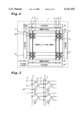
- a polycrystalline silicon semiconductor substrate is used as a substrate 1, and a pixel array 2 composed of an organic EL device and a peripheral driving integrated circuit 3 are formed on the substrate 1.
- the peripheral driving integrated circuit 3 comprises a Y driver 31 for feeding a scanning signal for displaying an image signal or the like on a screen to row selecting lines 4, an X driver 32 for feeding a data signal to data lines 5, and a sample/hold circuit 33 for sampling and holding video input signal data in accordance with a clock signal from the X driver 32.
- the substrate 1 is a monocrystalline silicon semiconductor substrate, and the Y driver 31, the X driver 32, and the sample/hold circuit 33 are formed in the periphery of the pixel array 2 by a known CMOS process.
- a Y clock and a Y start signal are fed to the Y driver 31, an X clock and an X start signal are fed to the X driver 32, and a video signal is fed to the sample/hold circuit 33.
- the row selecting lines 4 to which the horizontal scanning signal from the Y driver 31 is inputted are arranged parallel to each other through an insulating film on the substrate 1.
- the data lines 5 to which the data signal is fed are arranged similarly through the insulating film on the substrate 1.
- common electrode lines 6 are arranged parallel to each other through the insulating film on the substrate 1. As shown in FIGS. 3 and 4, a portion enclosed by the row selecting line 4, the data line 5, and the common electrode line 6 is an organic EL device 20 corresponding to one pixel.
- the number of pixels (organic EL devices) in two-dimensional arrangement is n ⁇ m
- the number of row selecting lines 4 and the number of common electrode lines 6 is n
- the number of data lines 5 is m.
- the organic EL device 20 is provided with switching means 21 for turning the organic EL device on and off.
- the switching means 21 comprises two MOS transistors (T1) and (Tr2) each having source and drain diffusion layers provided on the semiconductor substrate 1 and a capacitor (C).
- the MOS transistor (Tr1) has its gate (G) connected to the row selecting line 4, and has its drain (D) connected to the data line 5.
- the MOS transistor (Tr1) has its source (S) connected to the common electrode line 6 through the capacitor (C).
- the MOS transistor (Tr2) has its gate (G) connected to the source (S) of the MOS transistor (Tr1), and has its source (S) connected to the common electrode line 6.
- the MOS transistor (Tr2) has its drain (D) connected to one of pixel electrodes, that is, an anode (a transparent electrode) 24 in the present embodiment, and the other pixel electrode (a cathode) 22 is connected to the common electrode line 6.
- the MOS transistors (Tr1) and (Tr2) and the capacitor (C) are provided for each pixel.
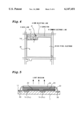
- the cathode 22 is arranged on the side of the semiconductor substrate 1, and an organic layer 23, and the transparent electrode 24, composed of ITO, SnO 2 , etc., serving as the anode are arranged thereon, so that the organic EL device 20 emits light from its surface opposite to the substrate 1, as shown in FIGS. 5 and 6.
- the organic EL device 20 emits light from its surface opposite to the substrate 1. Therefore, a light transmitting portion need not be formed by etching, for example, the substrate 1, the number of steps is not increased, and the mechanical strength may not be decreased.
- an insulating film 11 is formed on the silicon semiconductor substrate 1, and an electron injection electrode 22 (2000 ⁇ in thickness) serving as the cathode, an electron transporting layer 23a (500 ⁇ in thickness), a light emitting layer 23b (200 ⁇ in thickness), a hole transporting layer 23c (500 ⁇ in thickness), and a hole injection electrode 24, composed of an indium-tin oxide (ITO), serving as the anode are formed in this order on the insulating film 11.
- ITO indium-tin oxide
- the electron injection electrode (the cathode) 22 uses a metal having a small work function, for example, MgIn, MgAg, or AlLi. However, the cathode 22 easily reacts with oxygen or water in air because it has a small work function. If the cathode is arranged on the uppermost layer of the organic EL device, an antioxidant film for preventing the cathode from being oxidized is required. On the other hand, in the present invention, the cathode 22 which is easily oxidized is provided on the substrate 1, and the organic layer 23 and the anode (the transparent electrode) 24 are arranged thereon. Therefore, the cathode 22 can be prevented from being oxidized even if no special antioxidant film is provided by sealing the organic EL device using a sealing material and shield glass.
- a metal having a small work function for example, MgIn, MgAg, or AlLi.
- an antioxidant film for preventing the cathode from being oxidized is required.
- the hole transporting layer 23c, the light emitting layer 23b, and the electron transporting layer 23a respectively use organic EL materials.
- the hole transporting layer 23c is composed of a triphenyl amine derivative (MTDATA) indicated by the following chemical formula 1
- the light emitting layer 23b is composed of a material having as its host material N,N'-Diphenyl-N,N'-di( ⁇ -naphthyl)benzidine ( ⁇ NPD) indicated by the following chemical formula 2 and having rubrene indicated by the following chemical formula 3 doped into the host material
- the electron transporting layer 23a is composed of a 10-benzo(h)-quinolinolberyllium (BeBq 2 ) complex indicated by the following chemical formula 4.
- MOS transistors to be a peripheral driving integrated circuit 3 and switching means 21 in each of organic EL devices 20 in an organic EL pixel array 2 are respectively formed on a semiconductor substrate 1 using a normal MOS-LSI process technique.
- the peripheral driving integrated circuit 3 and the switching means 21 of the pixel are formed by the MOS-LSI process.
- Row selecting lines 4, data lines 5, and common electrode lines 6 are also provided on the substrate 1 through an insulating film 11, and are connected to the peripheral driving integrated circuit 3 and the switching means 21.
- the organic EL device 20 is formed in the organic EL pixel array 2.
- Cathodes 22 of the organic EL device 20 are first formed on the insulating film 11 on the semiconductor substrate 1.
- the cathodes 22 are formed, using a metal mask, in a predetermined pixel region on the semiconductor substrate 1 by resistance heating type vacuum evaporation.
- a material having a low work function for example, MgIn, MgAg or AlLi is used as a material for the cathodes 22.
- the pattern of the cathodes 22 is formed such that the common electrode line 6 and each of the cathodes 22 are electrically connected to each other.
- an organic electron transporting layer 23a, an organic light emitting layer 23b, and an organic hole transporting layer 23c are successively formed in this order similarly using vacuum evaporation on the entire surface of the substrate 1, including the cathodes 22, by masking the driving integrated circuit 3 and the switching means 21. That is, BeBq 2 is vacuum-evaporated over the cathodes 22, to form the electron transporting layer 23a, ⁇ NPD and rubrene are evaporated over the electron transporting layer 23a, to form the light emitting layer 23b, after which MTDATA is vacuum-evaporated over the light emitting layer 23b, to form the hole transporting layer 23c.
- the evaporation is performed under conditions that the degree of vacuum is 1 ⁇ 10 -6 Torr and the substrate temperature is not controlled.
- Transparent electrodes 24, composed of ITO, serving as anodes are formed in a predetermined pattern on an organic layer 23 by sputtering using a metal mask.
- the wiring steps using an aluminum film for connecting the organic EL device 20 and the driving integrated circuit 3 are then carried out.
- the driving integrated circuit 3 and the organic EL device 20 are electrically connected to each other, and are also connected to the transparent electrodes 24 and the switching means 21.
- the organic layer 23 dissolves in a resist liquid, so that aluminum wiring is done in a predetermined pattern using a metal mask.
- a protective film is formed on the entire surface of the organic EL pixel array 2 and the driving integrated circuit 3.
- a material for the protective film include a polymeric material (SiO), and metal oxides such as SiO 2 and MgO.
- FIG. 7 illustrates a second embodiment of an organic EL display device according to the present invention, which is a schematic view of a driving circuit integrated type organic EL display device in a passive and dynamic driving system.
- FIG. 8 is a diagram showing the schematic circuit structure thereof, and
- FIG. 9 is a schematic cross-sectional view thereof.
- a monocrystalline silicon semiconductor substrate is used as a substrate 1, and a pixel array 2 composed of an organic EL device and a peripheral driving integrated circuit 3a are formed on the substrate 1 as in above-mentioned first embodiment.
- the peripheral driving integrated circuit 3a comprises a Y driver 31a for feeding a scanning signal for displaying an image signal or the like on a screen to row selecting lines 4, an X electrode driver 33a for feeding a data signal to data lines 5, and a buffer memory 32a for holding video input signal data corresponding to one line in accordance with a clock signal from the X electrode driver 33a.
- the substrate 1 is a monocrystalline silicone semiconductor substrate, and the Y driver 31a, the X electrode driver 33a, and the buffer memory 32a are formed in the substrate 1 in the periphery of the pixel array 2 by a known CMOS process.
- the row selecting lines 4 to which the horizontal scanning signal fed from the Y driver 31a is inputted are arranged parallel to each other through an insulating film on the substrate 1.
- the data lines 5 are arranged parallel to each other in a direction perpendicular to the row selecting lines 4.
- the organic EL display device is driven by a passive and dynamic driving system, so that the organic EL device is provided between the data line 5 and the row selecting line 4.
- a cathode 22 is used as the row selecting line 4 in the pixel array 2, and an anode 24 is used as the data line 5.
- the cathodes 22 are arranged parallel to each other at the same pitch as the row selecting lines 4 from the Y driver 31a through the insulating film 11 on the substrate 1.
- An organic layer 23 is provided thereon, and the transparent electrodes 24 extending in a direction perpendicular to the cathodes 22 are arranged on the organic layer 23 at the same pitch as the data lines 5 from the X electrode driver 33a.
- the organic EL device is provided at the intersection of the row selecting line and the data line.
- the cathodes 22 are arranged on the side of the semiconductor substrate 1, the organic layer 23, and the transparent electrodes 24, composed of ITO, SnO 2 , etc., serving as the anodes are arranged thereon, so that the organic EL device emits light from its surface opposite to the substrate 1, as in the above-mentioned first embodiment. Also in the present embodiment, the organic EL device emits light from its surface opposite to the substrate 1. Also in the present embodiment, therefore, a light transmitting portion need not be formed by etching, for example, the substrate 1, the number of steps is not increased, and the mechanical strength may not be decreased.
- the organic EL device according to the present invention is constructed, similarly to the above-mentioned organic EL device. That is, an insulating film 11 is formed on the silicon semiconductor substrate 1, and an electron injection electrode 22 (2000 ⁇ in thickness) serving as the cathode, the organic layer 23 composed of an electron transporting layer (500 ⁇ in thickness), a light emitting layer (200 ⁇ in thickness)and a hole transporting layer (500 ⁇ in thickness), and a hole injection electrode 24, composed of an indium-tin oxide (ITO), serving as the anode are formed in this order on the insulating film 11. As described above, a deposited organic EL device is sealed using a sealing material and shield glass.
- ITO indium-tin oxide
- the cathode 22 which is easily oxidized is provided on the substrate 1, and the organic layer 23 and the anode (the transparent electrode) 24 are arranged thereon. Therefore, the cathodes 22 can be prevented from being oxidized, even if no antioxidant film is provided, by sealing the organic EL device using a sealing material and shield glass.
- a peripheral driving integrated circuit 3a is first formed on a semiconductor substrate 1 using a normal MOS-LSI process technique. After the process, an organic EL device is formed in an organic EL pixel array 2.
- Cathodes 22 of the organic EL device are first formed on an insulating film 11 on the semiconductor substrate 1.
- the cathodes 22 are formed, using a metal mask, parallel to each other at the same pitch as row selecting lines in a predetermined pixel area on the semiconductor substrate 1 by resistance heating type vacuum evaporation.
- a material having a low work function for example, MgIn, MgAg, or AlLi is used as a material for the cathodes 22.
- the pattern of the cathodes 22 is formed such that a common electrode line 6 and each of the cathodes 22 are electrically connected to each other.
- an organic electron transporting layer, an organic light emitting layer, and an organic hole transporting layer are successively formed in this order similarly using vacuum evaporation on the entire surface of the substrate 1, including the cathodes 22, by masking the driving integrated circuit 3a. That is, BeBq 2 is vacuum-evaporated over the cathodes 22, to form the electron transporting layer, and ⁇ NPD and rubrene are evaporated over the electron transporting layer, to form the light emitting layer, after which MTDATA is vacuum-evaporated over the light emitting layer, to form the hole transporting layer.
- the evaporation is performed under conditions that the degree of vacuum is 1 ⁇ 10 -6 Torr and the substrate temperature is not controlled.
- Transparent electrodes 24, composed of ITO, serving as anodes are formed in a predetermined pattern on an organic layer 23 by sputtering using a metal mask.
- the transparent electrodes 24 are patterned parallel to each other at the same pitch as the data lines in a direction perpendicular to the cathodes 22, so that the transparent electrode 24 and the X driver 33a are electrically connected to each other.
- a protective film is formed on the entire surface of the organic EL pixel array 2 and the driving integrated circuit 3a.
- a material for the protective film include a polymeric material (SiO), and metal oxides such as SiO 2 and MgO.
- the monocrystalline silicon substrate is used as the semiconductor substrate
- a polycrystalline silicon semiconductor layer formed on a glass substrate by a low-temperature process can be also used as a base substrate.
- a third embodiment of the present invention using as a base substrate a polycrystalline silicon semiconductor layer provided on a glass substrate will be described in FIGS. 10 and 11.
- an island composed of a polycrystalline silicon semiconductor is formed on a glass substrate 100 by a low-temperature process, and a pixel array composed of an organic EL device and a peripheral driving integrated circuit are formed on the substrate 100.
- a peripheral driving integrated circuit 112 is constituted by a driver, a register, or the like for displaying an image signal or the like on a screen, and comprises an n channel thin film transistor (TFT) 112a and a p-channel thin film transistor 112b.
- TFT thin film transistor
- row selecting lines to which a horizontal scanning signal from a driver circuit is inputted are arranged parallel to each other on the substrate 100, which is not illustrated.
- Data lines to which a data signal is fed are arranged on the substrate 100 similarly through an insulating film.
- common electrode lines are arranged parallel to each other through the insulating film on the substrate 100.
- a portion enclosed by the row selecting line, the data line, and the common electrode line is an organic EL device 120 corresponding to one pixel.
- the organic EL device 120 is provided with switching means for turning the organic EL device on and off.
- the switching means is constituted by a TFT 101 formed using a polycrystalline silicon island provided on the glass substrate 100.
- the organic EL device 120 is constituted by an active matrix four-terminal TFT-EL device, similarly to the above-mentioned organic EL device 20 shown in FIG. 3, and comprises two TFTs, a capacitor and an EL device.
- the polycrystalline silicon semiconductor is formed by a low-temperature process for melting and recrystallizing an amorphous silicon film formed by reduced pressure CVD on the glass substrate 100 using laser annealing.
- the polycrystalline silicon film formed on the glass substrate 100 is patterned by a photolithographic technique and a dry etching technique using RIE, to form a desired polycrystalline silicon island. Thereafter, a silicon oxide film to be a gate insulating film 104 is provided on the polycrystalline silicon island by reduced pressure CVD.
- a gate electrode 105 composed of tungsten silicide is formed on the gate insulating film 104. Impurities are injected into the polycrystalline silicon film using the gate electrode 105 as a mask by a self-aligning technique, to form a source region 102 and a drain region 103. Both the regions are activated by RTA (Rapid Thermal Annealing) or the like.
- An interlayer insulating film 106 composed of a silicon oxide film is formed on the TFT 101 by CVD.
- FIG. 10 is a cross-sectional view of a second TFT corresponding to the Tr2 shown in FIG. 3.
- a first TFT has its gate electrode connected to the row selecting line, and has its drain region connected to the data line, which is not illustrated.
- the first TFT has its source region connected to the common electrode line through a capacitor (C).
- the second TFT has its gate electrode 105 connected to the source region of the first TFT by aluminum wiring 107, and has its source region 102 connected to the common electrode line by the aluminum wiring 107.
- the second TFT has its drain region 103 connected to one of pixel electrodes, that is, an anode (a transparent electrode) 111 in the present embodiment, and the other pixel electrode (a cathode) 108 is connected to the common electrode line.
- the first and second TFTs and the capacitor (C) are provided for each pixel.
- the cathode 108 is arranged on the side of the glass substrate 100, and a passivation film 109, an organic layer 110, a transparent electrode 111, composed of ITO, SnO 2 , etc., serving as the anode are arranged thereon, so that the organic EL device emits light from its surface opposite to the glass substrate 100. That is, in the present embodiment, the organic EL device emits light from its surface opposite to the substrate 100.
- an electron injection electrode 108 (2000 ⁇ in thickness) serving as the cathode, an electron transporting layer (500 ⁇ in thickness), a light emitting layer (200 ⁇ in thickness), a hole transporting layer (500 ⁇ in thickness), and a hole injection electrode 111, composed of an indium-tin oxide (ITO), serving as the anode are formed in this order on an interlayer insulating film 106 provided on the glass substrate 100.
- a deposited organic EL device is sealed using a sealing material and shield glass.
- the above-mentioned electron injection electrode (the cathode) 108 uses a metal having a small work function, for example, MgIn, MgAg, or AlLi.
- the cathode 108 easily reacts with oxygen or water in air because it has a small work function. If the cathode is arranged on the uppermost layer of the organic EL device, therefore, an antioxidant film for preventing the cathode from being oxidized is required.
- the cathode 108 which is easily oxidized is provided on the glass substrate 100, and the organic layer 110 and the anode (the transparent electrode) 111 are arranged thereon. Therefore, the cathode 108 can be prevented from being oxidized even if no special antioxidant film is provided by sealing the organic EL device using a sealing material and shield glass.
- a polycrystalline silicon TFT for the peripheral driving integrated circuit is also formed on the same glass substrate 100 in the same fabricating method as the above-mentioned TFT for the organic EL device. Further, the polycrystalline silicon TFT for the peripheral driving integrated circuit is formed into a CMOS structure, so that the dimensions as each driver can be reduced.
- a driving circuit integrated type display device can be constructed using a glass substrate and a polycrystalline silicon semiconductor provided thereon in an organic EL display device in a passive and dynamic driving system as in the second embodiment.
- the organic EL display device is so constructed that the organic EL device emits light from its surface opposite to the glass substrate 100
- a substrate other than a transparent substrate can be also used as the substrate.
- the transparent substrate it can be so constructed that the organic EL device emits light from its surface on the side of the glass substrate, provided that the order in which the constituent elements of the organic EL device are arranged is reversed.
- the organic EL display device according to the present invention is suitably used for a direct view type display device, it can be also used as a light valve of a projector.
- the pixel array comprising the organic EL device and the peripheral driving integrated circuit can be produced on the same substrate, so that the organic EL display array is easy to fabricate, and can be miniaturized.
Abstract
Description
Claims (9)
Applications Claiming Priority (2)
| Application Number | Priority Date | Filing Date | Title |
|---|---|---|---|
| JP9-214724 | 1997-08-08 | ||
| JP9214724A JPH1154268A (en) | 1997-08-08 | 1997-08-08 | Organic electroluminescent display device |
Publications (1)
| Publication Number | Publication Date |
|---|---|
| US6147451A true US6147451A (en) | 2000-11-14 |
Family
ID=16660580
Family Applications (1)
| Application Number | Title | Priority Date | Filing Date |
|---|---|---|---|
| US09/129,837 Expired - Lifetime US6147451A (en) | 1997-08-08 | 1998-08-06 | Organic electrominiscent display device |
Country Status (2)
| Country | Link |
|---|---|
| US (1) | US6147451A (en) |
| JP (1) | JPH1154268A (en) |
Cited By (73)
| Publication number | Priority date | Publication date | Assignee | Title |
|---|---|---|---|---|
| EP1063630A2 (en) * | 1999-06-23 | 2000-12-27 | Semiconductor Energy Laboratory Co., Ltd. | Active matrix EL display device |
| US6281634B1 (en) | 1998-12-01 | 2001-08-28 | Sanyo Electric Co., Ltd. | Color electroluminescence display device |
| US6306694B1 (en) * | 1999-03-12 | 2001-10-23 | Semiconductor Energy Laboratory Co., Ltd. | Process of fabricating a semiconductor device |
| US20010033252A1 (en) * | 2000-04-18 | 2001-10-25 | Shunpei Yamazaki | Display device |
| US20010035713A1 (en) * | 2000-04-21 | 2001-11-01 | Semiconductor Energy Laboratory Co., Ltd. | Self-light emitting device and electrical appliance using the same |
| US20010055841A1 (en) * | 2000-04-17 | 2001-12-27 | Shunpei Yamazaki | Light emitting device and manufacturing method thereof |
| US20020021268A1 (en) * | 2000-08-18 | 2002-02-21 | Shunpei Yamazaki | Light emitting device |
| US6366026B1 (en) * | 1999-03-05 | 2002-04-02 | Sanyo Electric Co., Ltd. | Electroluminescence display apparatus |
| US20020047568A1 (en) * | 2000-07-27 | 2002-04-25 | Semiconductor Energy Laboratory Co., Ltd. | Method of driving display device |
| EP1207511A1 (en) * | 2000-03-30 | 2002-05-22 | Seiko Epson Corporation | Display |
| EP1227468A2 (en) * | 2001-01-30 | 2002-07-31 | Eastman Kodak Company | Method of integrating digital control and display devices on a common substrate |
| US6429599B1 (en) * | 1998-12-01 | 2002-08-06 | Sanyo Electric Co., Ltd. | Color electroluminescence display device |
| US6433486B1 (en) | 1998-12-01 | 2002-08-13 | Sanyo Electric Co., Ltd. | Color electroluminescence display device |
| US20020158829A1 (en) * | 2001-04-27 | 2002-10-31 | Semiconductor Energy Laboratory Co., Ltd. | Display system |
| US20030001800A1 (en) * | 2000-12-06 | 2003-01-02 | Yoshiharu Nakajima | Timing generating circuit for display and display having the same |
| US6541918B1 (en) * | 1998-03-12 | 2003-04-01 | Seiko Epson Corporation | Active-matrix emitting apparatus and fabrication method therefor |
| US20030132716A1 (en) * | 2000-06-13 | 2003-07-17 | Semiconductor Energy Laboratory Co., Ltd, A Japan Corporation | Display device |
| US20030146693A1 (en) * | 2002-02-06 | 2003-08-07 | Shingo Ishihara | Organic light-emitting display device |
| US20030151568A1 (en) * | 1997-07-02 | 2003-08-14 | Seiko Epson Corporation | Display apparatus |
| US20030151358A1 (en) * | 2002-02-12 | 2003-08-14 | Nec Corporation | Organic EL display device |
| US20030155594A1 (en) * | 2000-09-22 | 2003-08-21 | Semiconductor Energy Laboratory Co., Ltd. | Semiconductor display device and manufacturing method method thereof |
| US6641933B1 (en) * | 1999-09-24 | 2003-11-04 | Semiconductor Energy Laboratory Co., Ltd. | Light-emitting EL display device |
| US20030209721A1 (en) * | 2002-05-07 | 2003-11-13 | Toshiki Inoue | Semiconductor driver circuit, display device and method of adjusting brightness balance for display device |
| US6653750B2 (en) * | 1998-11-27 | 2003-11-25 | Sanyo Electric Co., Ltd. | Electroluminescence display apparatus for displaying gray scales |
| US20040008311A1 (en) * | 1997-08-21 | 2004-01-15 | Seiko Epson Corporation | Active matrix display device |
| US20040032213A1 (en) * | 2002-08-17 | 2004-02-19 | Lg Electronics Inc. | Flat display panel |
| US20040036071A1 (en) * | 1999-03-03 | 2004-02-26 | Semiconductor Energy Laboratory Co., Ltd. | Semiconductor device and method of fabricating the same |
| US20040056588A1 (en) * | 2002-08-30 | 2004-03-25 | Seiko Epson Corporation | Electro-optical device, method of manufacturing the same, and electronic apparatus |
| US20040135181A1 (en) * | 2000-02-28 | 2004-07-15 | Semiconductor Energy Laboratory Co., Ltd. A Japan Corporation | Electronic device |
| US20040160170A1 (en) * | 2002-12-11 | 2004-08-19 | Chiyoko Sato | Display apparatus and method of manufacturing the same |
| US20040195576A1 (en) * | 2003-03-14 | 2004-10-07 | Toshihiko Watanabe | Light-emitting device, light-emitting apparatus, image display apparatus, method of manufacturing light-emitting device, and method of manufacturing image display apparatus |
| US20040257539A1 (en) * | 2002-08-16 | 2004-12-23 | Peterson Mark D. | Projection television device and screen |
| US20050006667A1 (en) * | 1999-06-28 | 2005-01-13 | Semiconductor Energy Laboratory Co., Ltd. | EL display device and electronic device |
| US6847163B1 (en) * | 1999-10-29 | 2005-01-25 | Semiconductor Energy Laboratory Co., Ltd. | Self light-emitting device using an inert gas |
| US6853083B1 (en) * | 1995-03-24 | 2005-02-08 | Semiconductor Energy Laboratory Co., Ltd. | Thin film transfer, organic electroluminescence display device and manufacturing method of the same |
| US6876007B2 (en) * | 2001-11-22 | 2005-04-05 | Semiconductor Energy Laboratory Co., Ltd. | Light emitting device driving by alternating current in which light emission is always obtained |
| US20050073242A1 (en) * | 1999-06-21 | 2005-04-07 | Semiconductor Energy Laboratory Co., Ltd. | EL display device, driving method thereof, and electronic equipment provided with the display device |
| US20050099118A1 (en) * | 2003-08-18 | 2005-05-12 | Seiko Epson Corporation | Organic EL device, method of manufacturing the same and electronic apparatus |
| US20050100832A1 (en) * | 1998-11-11 | 2005-05-12 | Semiconductor Energy Laboratory Co., Ltd. | Exposure device, exposure method and method of manufacturing semiconductor device |
| US20050156173A1 (en) * | 1999-09-30 | 2005-07-21 | Semiconductor Energy Laboratory Co., Ltd. | Organic electroluminescent display device |
| US20050190130A1 (en) * | 2002-01-11 | 2005-09-01 | Takayuki Ouchi | Active matrix type display |
| US6940214B1 (en) * | 1999-02-09 | 2005-09-06 | Sanyo Electric Co., Ltd. | Electroluminescence display device |
| US6972746B1 (en) * | 1994-10-31 | 2005-12-06 | Semiconductor Energy Laboratory Co., Ltd. | Active matrix type flat-panel display device |
| US20050282304A1 (en) * | 2001-12-18 | 2005-12-22 | Seiko Epson Corporation | Light-emission device, method of manufacturing same, electro-optical device and electronic device |
| US20060017380A1 (en) * | 2000-02-03 | 2006-01-26 | Semiconductor Energy Laboratory Co., Ltd., A Japan Corporation | Light-emitting device and method of manufacturing the same |
| US7001060B1 (en) | 1999-08-11 | 2006-02-21 | Semiconductor Energy Laboratory Co., Ltd. | Front light having a plurality of prism-shaped lenses |
| US20060063028A1 (en) * | 2003-04-08 | 2006-03-23 | Leurs Jeroom Frans M | Two sided light emitting device |
| US20060077651A1 (en) * | 2001-02-15 | 2006-04-13 | Semiconductor Energy Laboratory Co., Ltd. | EL display device and electronic device |
| US20060183323A1 (en) * | 2005-02-14 | 2006-08-17 | Omnivision Technologies, Inc. | Salicide process using CMP for image sensor |
| US7119767B1 (en) * | 1999-09-29 | 2006-10-10 | Sanyo Electric Co., Ltd. | Active matrix type electroluminescence display device |
| US7235810B1 (en) | 1998-12-03 | 2007-06-26 | Semiconductor Energy Laboratory Co., Ltd. | Semiconductor device and method of fabricating the same |
| US20070159777A1 (en) * | 2005-12-22 | 2007-07-12 | Dong-Hyok Shin | Chassis assembly and display apparatus having the same |
| US20070247064A1 (en) * | 2000-02-16 | 2007-10-25 | Idemitsu Kosan Co., Ltd. | Actively driven organic el device and manufacturing method thereof |
| US20080029765A1 (en) * | 1999-10-29 | 2008-02-07 | Semiconductor Energy Laboratory Co., Ltd. | Electronic Device |
| US20080036699A1 (en) * | 1997-08-21 | 2008-02-14 | Seiko Epson Corporation | Active matrix display device |
| WO2008083671A1 (en) * | 2007-01-11 | 2008-07-17 | Osram Opto Semiconductors Gmbh | Optoelectronic device, and method for the production thereof |
| US20080213482A1 (en) * | 2007-03-01 | 2008-09-04 | Stephan Lvovich Logunov | Method of making a mask for sealing a glass package |
| US20090001896A1 (en) * | 2002-02-22 | 2009-01-01 | Semiconductor Energy Laboratory Co., Ltd. | Light-Emitting Device and Method of Manufacturing the Same, and Method of Operating Manufacturing Apparatus |
| US7697052B1 (en) * | 1999-02-17 | 2010-04-13 | Semiconductor Energy Laboratory Co., Ltd. | Electronic view finder utilizing an organic electroluminescence display |
| US7701134B2 (en) | 1999-06-04 | 2010-04-20 | Semiconductor Energy Laboratory Co., Ltd. | Active matrix display device with improved operating performance |
| US7786958B1 (en) | 1999-09-24 | 2010-08-31 | Semiconductor Energy Laboratory Co., Ltd. | EL display device and electronic device |
| US20100244005A1 (en) * | 2009-03-26 | 2010-09-30 | Seiko Epson Corporation | Organic el apparatus, method of manufacturing organic el apparatus, electronic apparatus |
| US20110207248A1 (en) * | 2000-10-26 | 2011-08-25 | Semiconductor Energy Laboratory Co., Ltd. | Light Emitting Device and Manufacturing Method Thereof |
| US8194006B2 (en) | 2004-08-23 | 2012-06-05 | Semiconductor Energy Laboratory Co., Ltd. | Display device, driving method of the same, and electronic device comprising monitoring elements |
| JP2014056242A (en) * | 1999-03-02 | 2014-03-27 | Semiconductor Energy Lab Co Ltd | Semiconductor device |
| US8957584B2 (en) | 1999-10-29 | 2015-02-17 | Semiconductor Energy Laboratory Co., Ltd. | Self light-emitting device |
| US9159948B2 (en) | 2013-03-21 | 2015-10-13 | Semiconductor Energy Laboratory Co., Ltd. | Display device including light-emitting element and electronic device |
| US20150349287A1 (en) * | 2014-05-28 | 2015-12-03 | Samsung Display Co., Ltd. | Organic light-emitting display apparatus and method of manufacturing the same |
| US20160077341A1 (en) * | 2010-10-08 | 2016-03-17 | Seiko Epson Corporation | Virtual image display apparatus |
| US9343515B2 (en) | 2013-03-21 | 2016-05-17 | Semiconductor Energy Laboratory Co., Ltd. | Display device, manufacturing method thereof, and electronic device |
| US9443461B2 (en) | 2000-04-19 | 2016-09-13 | Semiconductor Energy Laboratory Co., Ltd. | Electronic device and method of driving the same |
| US20160365029A1 (en) * | 2000-01-17 | 2016-12-15 | Semiconductor Energy Laboratory Co., Ltd. | Display system and electrical appliance |
| US9837451B2 (en) | 1999-04-27 | 2017-12-05 | Semiconductor Energy Laboratory Co., Ltd. | Electronic device and electronic apparatus |
Families Citing this family (8)
| Publication number | Priority date | Publication date | Assignee | Title |
|---|---|---|---|---|
| GB9907931D0 (en) * | 1999-04-07 | 1999-06-02 | Univ Edinburgh | An optoelectronic display |
| JP3942770B2 (en) * | 1999-09-22 | 2007-07-11 | 株式会社半導体エネルギー研究所 | EL display device and electronic device |
| JP5025040B2 (en) * | 1999-09-30 | 2012-09-12 | 株式会社半導体エネルギー研究所 | Self-luminous device |
| US6384427B1 (en) * | 1999-10-29 | 2002-05-07 | Semiconductor Energy Laboratory Co., Ltd. | Electronic device |
| JP2001195016A (en) * | 1999-10-29 | 2001-07-19 | Semiconductor Energy Lab Co Ltd | Electronic device |
| JP4758163B2 (en) * | 2000-02-03 | 2011-08-24 | 株式会社半導体エネルギー研究所 | Light emitting device |
| KR20030044568A (en) * | 2001-11-30 | 2003-06-09 | 오리온전기 주식회사 | Method for manufacturing an passive matrix organic electroluminescent panel and display operating system thereof |
| JP5609941B2 (en) * | 2012-09-26 | 2014-10-22 | セイコーエプソン株式会社 | Display device and electronic device |
Citations (3)
| Publication number | Priority date | Publication date | Assignee | Title |
|---|---|---|---|---|
| US5550066A (en) * | 1994-12-14 | 1996-08-27 | Eastman Kodak Company | Method of fabricating a TFT-EL pixel |
| US5602445A (en) * | 1995-05-12 | 1997-02-11 | Oregon Graduate Institute Of Science And Technology | Blue-violet phosphor for use in electroluminescent flat panel displays |
| US5612591A (en) * | 1994-12-29 | 1997-03-18 | Nippondenso Co., Ltd. | Electroluminescent device |
-
1997
- 1997-08-08 JP JP9214724A patent/JPH1154268A/en active Pending
-
1998
- 1998-08-06 US US09/129,837 patent/US6147451A/en not_active Expired - Lifetime
Patent Citations (3)
| Publication number | Priority date | Publication date | Assignee | Title |
|---|---|---|---|---|
| US5550066A (en) * | 1994-12-14 | 1996-08-27 | Eastman Kodak Company | Method of fabricating a TFT-EL pixel |
| US5612591A (en) * | 1994-12-29 | 1997-03-18 | Nippondenso Co., Ltd. | Electroluminescent device |
| US5602445A (en) * | 1995-05-12 | 1997-02-11 | Oregon Graduate Institute Of Science And Technology | Blue-violet phosphor for use in electroluminescent flat panel displays |
Non-Patent Citations (1)
| Title |
|---|
| Patent Abstracts of Japan, Publication No. 09114398A, May 2, 1997. * |
Cited By (241)
| Publication number | Priority date | Publication date | Assignee | Title |
|---|---|---|---|---|
| US20060033690A1 (en) * | 1994-10-31 | 2006-02-16 | Semiconductor Energy Laboratory Co., Ltd. | Active matrix type flat-panel display device |
| US6972746B1 (en) * | 1994-10-31 | 2005-12-06 | Semiconductor Energy Laboratory Co., Ltd. | Active matrix type flat-panel display device |
| US7298357B2 (en) | 1994-10-31 | 2007-11-20 | Semiconductor Energy Laboratory Co., Ltd. | Active matrix type flat-panel display device |
| US20060087222A1 (en) * | 1995-03-24 | 2006-04-27 | Semiconductor Energy Laboratory Co., Ltd. | Thin film transistor, organic electroluminescence display device and manufacturing method of the same |
| US6992435B2 (en) | 1995-03-24 | 2006-01-31 | Semiconductor Energy Laboratory Co., Ltd. | Thin film transistor, organic electroluminescence display device and manufacturing method of the same |
| US20050146262A1 (en) * | 1995-03-24 | 2005-07-07 | Semiconductor Energy Laboratory Co., Ltd. | Thin film transistor, organic electroluminescence display device and manufacturing method of the same |
| US6853083B1 (en) * | 1995-03-24 | 2005-02-08 | Semiconductor Energy Laboratory Co., Ltd. | Thin film transfer, organic electroluminescence display device and manufacturing method of the same |
| US7476900B2 (en) | 1995-03-24 | 2009-01-13 | Semiconductor Energy Laboratory Co., Ltd. | Thin film transistor, organic electroluminescence display device and manufacturing method of the same |
| US20080165174A1 (en) * | 1997-07-02 | 2008-07-10 | Seiko Epson Corporation | Display apparatus |
| US8310476B2 (en) | 1997-07-02 | 2012-11-13 | Seiko Epson Corporation | Display apparatus |
| US8310475B2 (en) | 1997-07-02 | 2012-11-13 | Seiko Epson Corporation | Display apparatus |
| US20080198152A1 (en) * | 1997-07-02 | 2008-08-21 | Seiko Epson Corporation | Display apparatus |
| US8334858B2 (en) | 1997-07-02 | 2012-12-18 | Seiko Epson Corporation | Display apparatus |
| US20030151568A1 (en) * | 1997-07-02 | 2003-08-14 | Seiko Epson Corporation | Display apparatus |
| US20080158209A1 (en) * | 1997-07-02 | 2008-07-03 | Seiko Epson Corporation | Display apparatus |
| US8803773B2 (en) | 1997-07-02 | 2014-08-12 | Intellectual Keystone Technology Llc | Display apparatus |
| US20080180421A1 (en) * | 1997-08-21 | 2008-07-31 | Seiko Epson Corporation | Active matrix display device |
| US8159124B2 (en) | 1997-08-21 | 2012-04-17 | Seiko Epson Corporation | Active matrix display device |
| US20100045577A1 (en) * | 1997-08-21 | 2010-02-25 | Seiko Epson Corporation | Active matrix display device |
| US20050170096A1 (en) * | 1997-08-21 | 2005-08-04 | Seiko Epson Corporation | Active matrix display device |
| US20090303165A1 (en) * | 1997-08-21 | 2009-12-10 | Seiko Epson Corporation | Active matrix display device |
| US7364939B2 (en) | 1997-08-21 | 2008-04-29 | Seiko Epson Corporation | Active matrix display device |
| US20080036699A1 (en) * | 1997-08-21 | 2008-02-14 | Seiko Epson Corporation | Active matrix display device |
| US20040008311A1 (en) * | 1997-08-21 | 2004-01-15 | Seiko Epson Corporation | Active matrix display device |
| US6885148B2 (en) * | 1997-08-21 | 2005-04-26 | Seiko Epson Corporation | Active matrix display device |
| US6541918B1 (en) * | 1998-03-12 | 2003-04-01 | Seiko Epson Corporation | Active-matrix emitting apparatus and fabrication method therefor |
| US20080316449A1 (en) * | 1998-11-11 | 2008-12-25 | Semiconductor Energy Laboratory Co., Ltd. | Exposure Device, Exposure Method and Method of Manufacturing Semiconductor Device |
| US20050100832A1 (en) * | 1998-11-11 | 2005-05-12 | Semiconductor Energy Laboratory Co., Ltd. | Exposure device, exposure method and method of manufacturing semiconductor device |
| US8859947B2 (en) | 1998-11-11 | 2014-10-14 | Semiconductor Energy Laboratory Co., Ltd. | Display device comprising at least dual transistor electrically connected to dual parallel wiring |
| US7022556B1 (en) | 1998-11-11 | 2006-04-04 | Semiconductor Energy Laboratory Co., Ltd. | Exposure device, exposure method and method of manufacturing semiconductor device |
| US8297991B2 (en) | 1998-11-11 | 2012-10-30 | Semiconductor Energy Laboratory Co., Ltd. | Exposure device, exposure method and method of manufacturing semiconductor device |
| US9366971B2 (en) | 1998-11-11 | 2016-06-14 | Semiconductor Energy Laboratory Co., Ltd. | Display device comprising dual transistor with LDD regions overlapping the gate electrodes and one of a source electrode and a drain electrode of first transistor is electrically connected to the second gate electrode |
| US8476665B2 (en) | 1998-11-11 | 2013-07-02 | Semiconductor Energy Laboratory Co., Ltd. | Display device |
| US7405432B2 (en) | 1998-11-11 | 2008-07-29 | Semiconductor Energy Laboratory Co., Ltd. | Exposure device, exposure method and method of manufacturing semiconductor device |
| US6653750B2 (en) * | 1998-11-27 | 2003-11-25 | Sanyo Electric Co., Ltd. | Electroluminescence display apparatus for displaying gray scales |
| US6690118B2 (en) | 1998-12-01 | 2004-02-10 | Sanyo Electric Co., Ltd. | Color electroluminescence display device |
| US6995517B2 (en) | 1998-12-01 | 2006-02-07 | Sanyo Electric Co., Ltd. | Color electroluminescence display device |
| US6433486B1 (en) | 1998-12-01 | 2002-08-13 | Sanyo Electric Co., Ltd. | Color electroluminescence display device |
| US20030011316A1 (en) * | 1998-12-01 | 2003-01-16 | Ryoichi Yokoyama | Color electroluminescence display device |
| US20060197461A1 (en) * | 1998-12-01 | 2006-09-07 | Ryoichi Yokoyama | Color electroluminescence display device |
| US6281634B1 (en) | 1998-12-01 | 2001-08-28 | Sanyo Electric Co., Ltd. | Color electroluminescence display device |
| US7339559B2 (en) | 1998-12-01 | 2008-03-04 | Sanyo Electric Co., Ltd. | Color electroluminescence display device |
| US6429599B1 (en) * | 1998-12-01 | 2002-08-06 | Sanyo Electric Co., Ltd. | Color electroluminescence display device |
| US7315131B2 (en) | 1998-12-01 | 2008-01-01 | Sanyo Electric Co., Ltd. | Color electroluminescence display device |
| US20040130514A1 (en) * | 1998-12-01 | 2004-07-08 | Ryoichi Yokoyama | Color electroluminescence display device |
| US7776712B2 (en) | 1998-12-03 | 2010-08-17 | Semiconductor Energy Laboratory Co., Ltd. | Method of forming a semiconductor device |
| US7235810B1 (en) | 1998-12-03 | 2007-06-26 | Semiconductor Energy Laboratory Co., Ltd. | Semiconductor device and method of fabricating the same |
| US6940214B1 (en) * | 1999-02-09 | 2005-09-06 | Sanyo Electric Co., Ltd. | Electroluminescence display device |
| US7697052B1 (en) * | 1999-02-17 | 2010-04-13 | Semiconductor Energy Laboratory Co., Ltd. | Electronic view finder utilizing an organic electroluminescence display |
| JP2014056242A (en) * | 1999-03-02 | 2014-03-27 | Semiconductor Energy Lab Co Ltd | Semiconductor device |
| US9153604B2 (en) | 1999-03-02 | 2015-10-06 | Semiconductor Energy Laboratory Co., Ltd. | Semiconductor device and method of manufacturing the same |
| US8847316B2 (en) | 1999-03-02 | 2014-09-30 | Semiconductor Energy Laboratory Co., Ltd. | Semiconductor device and method of manufacturing the same |
| US20070164290A1 (en) * | 1999-03-03 | 2007-07-19 | Semiconductor Energy Laboratory Co., Ltd. | Semiconductor device and method of fabricating the same |
| US7161176B2 (en) | 1999-03-03 | 2007-01-09 | Semiconductor Energy Laboratory Co., Ltd. | Electroluminescence display device having a semiconductor substrate |
| US20040036071A1 (en) * | 1999-03-03 | 2004-02-26 | Semiconductor Energy Laboratory Co., Ltd. | Semiconductor device and method of fabricating the same |
| US7723725B2 (en) | 1999-03-03 | 2010-05-25 | Semiconductor Energy Laboratory Co., Ltd. | Semiconductor device and method of fabricating the same |
| US6366026B1 (en) * | 1999-03-05 | 2002-04-02 | Sanyo Electric Co., Ltd. | Electroluminescence display apparatus |
| US6737304B2 (en) | 1999-03-12 | 2004-05-18 | Semiconductor Energy Laboratory Co., Ltd. | Process of fabricating a semiconductor device |
| US6306694B1 (en) * | 1999-03-12 | 2001-10-23 | Semiconductor Energy Laboratory Co., Ltd. | Process of fabricating a semiconductor device |
| US7351619B2 (en) | 1999-03-12 | 2008-04-01 | Semiconductor Energy Laboratory Co., Ltd. | Process of fabricating a semiconductor device |
| US20040197971A1 (en) * | 1999-03-12 | 2004-10-07 | Semiconductor Energy Laboratory Co., Ltd. | Process of fabricating a semiconductor device |
| US9837451B2 (en) | 1999-04-27 | 2017-12-05 | Semiconductor Energy Laboratory Co., Ltd. | Electronic device and electronic apparatus |
| US9368680B2 (en) | 1999-06-04 | 2016-06-14 | Semiconductor Energy Laboratory Co., Ltd. | Electro-optical device and electronic device |
| US8853696B1 (en) | 1999-06-04 | 2014-10-07 | Semiconductor Energy Laboratory Co., Ltd. | Electro-optical device and electronic device |
| US8227809B2 (en) | 1999-06-04 | 2012-07-24 | Semiconductor Energy Laboratory Co., Ltd. | Electro-optical device and electronic device |
| US7741775B2 (en) | 1999-06-04 | 2010-06-22 | Semiconductor Energy Laboratories Co., Ltd. | Electro-optical device and electronic device |
| US7701134B2 (en) | 1999-06-04 | 2010-04-20 | Semiconductor Energy Laboratory Co., Ltd. | Active matrix display device with improved operating performance |
| US9123854B2 (en) | 1999-06-04 | 2015-09-01 | Semiconductor Energy Laboratory Co., Ltd. | Electro-optical device and electronic device |
| US9659524B2 (en) | 1999-06-21 | 2017-05-23 | Semiconductor Energy Laboratory Co., Ltd. | Light-emitting device including substrate having cavity, and method for fabricating the light-emitting device |
| US8830146B2 (en) | 1999-06-21 | 2014-09-09 | Semiconductor Energy Laboratory Co., Ltd. | EL display device, driving method thereof, and electronic equipment provided with the EL display device |
| US7821200B2 (en) | 1999-06-21 | 2010-10-26 | Semiconductor Energy Laboratory Co., Ltd. | EL display device, driving method thereof, and electronic equipment provided with the EL display device |
| US7466293B2 (en) * | 1999-06-21 | 2008-12-16 | Semiconductor Energy Laboratory Co., Ltd. | EL display device, driving method thereof, and electronic equipment provided with the EL display device |
| US20050073242A1 (en) * | 1999-06-21 | 2005-04-07 | Semiconductor Energy Laboratory Co., Ltd. | EL display device, driving method thereof, and electronic equipment provided with the display device |
| US8941565B2 (en) | 1999-06-21 | 2015-01-27 | Semiconductor Energy Laboratory Co., Ltd. | EL display device, driving method thereof, and electronic equipment provided with the EL display device |
| US8558773B2 (en) | 1999-06-21 | 2013-10-15 | Semiconductor Energy Laboratory Co., Ltd. | EL display device, driving method thereof, and electronic equipment provided with the EL display device |
| US8405594B2 (en) | 1999-06-21 | 2013-03-26 | Semiconductor Energy Laboratory Co., Ltd. | EL display device, driving method thereof, and electronic equipment provided with the EL display device |
| EP1063630A2 (en) * | 1999-06-23 | 2000-12-27 | Semiconductor Energy Laboratory Co., Ltd. | Active matrix EL display device |
| US20040207331A1 (en) * | 1999-06-23 | 2004-10-21 | Semiconductor Energy Laboratory Co., Ltd. | El display device and electronic device |
| EP2372682A3 (en) * | 1999-06-23 | 2012-05-30 | Semiconductor Energy Laboratory Co, Ltd. | Active matrix EL display device |
| US6774574B1 (en) | 1999-06-23 | 2004-08-10 | Semiconductor Energy Laboratory Co., Ltd. | EL display device and electronic device |
| US7982222B2 (en) | 1999-06-23 | 2011-07-19 | Semiconductor Energy Laboratory Co., Ltd. | EL display device and electronic device |
| EP1063630A3 (en) * | 1999-06-23 | 2002-07-10 | Semiconductor Energy Laboratory Co., Ltd. | Active matrix EL display device |
| US7358531B2 (en) | 1999-06-23 | 2008-04-15 | Semiconductor Energy Laboratory Co., Ltd. | EL display device and electronic device |
| US6777887B2 (en) | 1999-06-23 | 2004-08-17 | Semiconductor Energy Laboratory Co., Ltd. | EL display device and electronic device |
| US7256422B2 (en) | 1999-06-28 | 2007-08-14 | Semiconductor Energy Laboratory Co., Ltd. | EL display device and electronic device |
| US20080024069A1 (en) * | 1999-06-28 | 2008-01-31 | Semiconductor Energy Laboratory Co., Ltd. | EL display device and electronic device |
| US20050006667A1 (en) * | 1999-06-28 | 2005-01-13 | Semiconductor Energy Laboratory Co., Ltd. | EL display device and electronic device |
| EP1065723A3 (en) * | 1999-06-28 | 2006-05-24 | Sel Semiconductor Energy Laboratory Co., Ltd. | EL display device and electronic device |
| US7548027B2 (en) | 1999-06-28 | 2009-06-16 | Semiconductor Energy Laboratory Co., Ltd. | EL display device and electronic device |
| US7001060B1 (en) | 1999-08-11 | 2006-02-21 | Semiconductor Energy Laboratory Co., Ltd. | Front light having a plurality of prism-shaped lenses |
| US8053979B2 (en) | 1999-09-24 | 2011-11-08 | Semiconductor Energy Laboratory Co., Ltd. | Light-emitting organic compound with improved reliability |
| US8436790B2 (en) | 1999-09-24 | 2013-05-07 | Semiconductor Energy Laboratory Co., Ltd. | EL display device and electronic device |
| US8698389B2 (en) | 1999-09-24 | 2014-04-15 | Semiconductor Energy Laboratory Co., Ltd. | Light-emitting organic compound and EL display device utilizing the same |
| US20070007870A1 (en) * | 1999-09-24 | 2007-01-11 | Semiconductor Energy Laboratory Co., Ltd. | Light-emitting organic compound and EL display device utilizing the same |
| US7786958B1 (en) | 1999-09-24 | 2010-08-31 | Semiconductor Energy Laboratory Co., Ltd. | EL display device and electronic device |
| US6641933B1 (en) * | 1999-09-24 | 2003-11-04 | Semiconductor Energy Laboratory Co., Ltd. | Light-emitting EL display device |
| US9425403B2 (en) | 1999-09-24 | 2016-08-23 | Semiconductor Energy Laboratory Co., Ltd. | Light-emitting organic compound and EL display device utilizing the same |
| US7112374B2 (en) | 1999-09-24 | 2006-09-26 | Semiconductor Energy Laboratory Co., Ltd. | EL display device utilizing light-emitting organic compounds and method for forming the same |
| US20100321281A1 (en) * | 1999-09-24 | 2010-12-23 | Semiconductor Energy Laboratory Co., Ltd. | EL Display Device and Electronic Device |
| US7119767B1 (en) * | 1999-09-29 | 2006-10-10 | Sanyo Electric Co., Ltd. | Active matrix type electroluminescence display device |
| US8426876B2 (en) | 1999-09-30 | 2013-04-23 | Semiconductor Energy Laboratory Co., Ltd. | Organic electroluminescent display device |
| US7838883B2 (en) | 1999-09-30 | 2010-11-23 | Semiconductor Energy Laboratory Co., Ltd. | Organic electroluminescent display device |
| US8772766B2 (en) | 1999-09-30 | 2014-07-08 | Semiconductor Energy Laboratory Co., Ltd. | Organic electroluminescent display device |
| US9853235B2 (en) | 1999-09-30 | 2017-12-26 | Semiconductor Energy Laboratory Co., Ltd. | Organic electroluminescent display device |
| US20050156173A1 (en) * | 1999-09-30 | 2005-07-21 | Semiconductor Energy Laboratory Co., Ltd. | Organic electroluminescent display device |
| US8110983B2 (en) | 1999-10-29 | 2012-02-07 | Semiconductor Energy Laboratory Co., Ltd. | Self light emitting device |
| US20050099120A1 (en) * | 1999-10-29 | 2005-05-12 | Semiconductor Energy Laboratory Co., Ltd. | Self light-emitting device |
| US9299955B2 (en) | 1999-10-29 | 2016-03-29 | Semiconductor Energy Laboratory Co., Ltd. | Self light-emitting device |
| US8957584B2 (en) | 1999-10-29 | 2015-02-17 | Semiconductor Energy Laboratory Co., Ltd. | Self light-emitting device |
| US20060267483A1 (en) * | 1999-10-29 | 2006-11-30 | Semiconductor Energy Laboratory Co., Ltd. | Self light-emitting device |
| US7317282B2 (en) | 1999-10-29 | 2008-01-08 | Semiconductor Energy Laboratory Co., Ltd. | Self light-emitting device |
| US6847163B1 (en) * | 1999-10-29 | 2005-01-25 | Semiconductor Energy Laboratory Co., Ltd. | Self light-emitting device using an inert gas |
| US20080029765A1 (en) * | 1999-10-29 | 2008-02-07 | Semiconductor Energy Laboratory Co., Ltd. | Electronic Device |
| US8648345B2 (en) | 1999-10-29 | 2014-02-11 | Semiconductor Energy Laboratory Co., Ltd. | Electronic device |
| US8017945B2 (en) | 1999-10-29 | 2011-09-13 | Semiconductor Energy Laboratory Co., Ltd. | Display device using light-emitting element |
| US10522076B2 (en) * | 2000-01-17 | 2019-12-31 | Semiconductor Energy Laboratory Co., Ltd. | Display system and electrical appliance |
| US10467961B2 (en) | 2000-01-17 | 2019-11-05 | Semiconductor Energy Laboratory Co., Ltd. | Display system and electrical appliance |
| US20160365029A1 (en) * | 2000-01-17 | 2016-12-15 | Semiconductor Energy Laboratory Co., Ltd. | Display system and electrical appliance |
| US7745993B2 (en) | 2000-02-03 | 2010-06-29 | Semiconductor Energy Laboratory Co., Ltd. | Method for manufacturing light emitting device comprising reflective film |
| US20060038488A1 (en) * | 2000-02-03 | 2006-02-23 | Semiconductor Energy Laboratory Co., Ltd., A Japan Corporation | Method for manufacturing light emitting device comprising reflective film |
| US20110101852A1 (en) * | 2000-02-03 | 2011-05-05 | Semiconductor Energy Laboratory Co., Ltd. | Light-emitting device and method of manufacturing the same |
| US7867053B2 (en) | 2000-02-03 | 2011-01-11 | Semiconductor Energy Laboratory Co., Ltd. | Method for manufacturing light emitting device |
| US20060017380A1 (en) * | 2000-02-03 | 2006-01-26 | Semiconductor Energy Laboratory Co., Ltd., A Japan Corporation | Light-emitting device and method of manufacturing the same |
| US7683535B2 (en) | 2000-02-03 | 2010-03-23 | Semiconductor Energy Laboratory Co., Ltd. | Light-emitting device and method of manufacturing the same |
| US20070197118A1 (en) * | 2000-02-03 | 2007-08-23 | Semiconductor Energy Laboratory Co., Ltd. | Method for Manufacturing Light Emitting Device |
| US8810130B2 (en) | 2000-02-03 | 2014-08-19 | Semiconductor Energy Laboratory Co., Ltd. | Light-emitting device and method of manufacturing the same |
| US8339038B2 (en) | 2000-02-03 | 2012-12-25 | Semiconductor Energy Laboratory Co., Ltd. | Light-emitting device |
| US9419066B2 (en) | 2000-02-03 | 2016-08-16 | Semiconductor Energy Laboratory Co., Ltd. | Light-emitting device and method of manufacturing the same |
| US7994705B2 (en) * | 2000-02-16 | 2011-08-09 | Idemitsu Kosan Co. | Actively driven organic EL device and manufacturing method thereof |
| US20070247064A1 (en) * | 2000-02-16 | 2007-10-25 | Idemitsu Kosan Co., Ltd. | Actively driven organic el device and manufacturing method thereof |
| US8017944B2 (en) * | 2000-02-28 | 2011-09-13 | Semiconductor Energy Laboratory Co., Ltd. | Electronic device with light emission for a display |
| US8829668B2 (en) | 2000-02-28 | 2014-09-09 | Semiconductor Energy Laboratory Co., Ltd. | Electronic device |
| US20040135181A1 (en) * | 2000-02-28 | 2004-07-15 | Semiconductor Energy Laboratory Co., Ltd. A Japan Corporation | Electronic device |
| EP1207511A1 (en) * | 2000-03-30 | 2002-05-22 | Seiko Epson Corporation | Display |
| EP1207511A4 (en) * | 2000-03-30 | 2006-08-16 | Seiko Epson Corp | Display |
| US7820464B2 (en) | 2000-04-17 | 2010-10-26 | Semiconductor Energy Laboratory Co., Ltd. | Light emitting device and manufacturing method thereof |
| US7525165B2 (en) * | 2000-04-17 | 2009-04-28 | Semiconductor Energy Laboratory Co., Ltd. | Light emitting device and manufacturing method thereof |
| US20010055841A1 (en) * | 2000-04-17 | 2001-12-27 | Shunpei Yamazaki | Light emitting device and manufacturing method thereof |
| US7990348B2 (en) | 2000-04-18 | 2011-08-02 | Semiconductor Energy Laboratory Co., Ltd. | Display device |
| US20110140997A1 (en) * | 2000-04-18 | 2011-06-16 | Semiconductor Energy Laboratory Co., Ltd. | Display device |
| US8400379B2 (en) | 2000-04-18 | 2013-03-19 | Semiconductor Energy Laboratory Co., Ltd. | Display device |
| US7623099B2 (en) | 2000-04-18 | 2009-11-24 | Semiconductor Energy Laboratory Co., Ltd. | Display device |
| US7623100B2 (en) | 2000-04-18 | 2009-11-24 | Semiconductor Energy Laboratory Co., Ltd. | Display device |
| US7623098B2 (en) | 2000-04-18 | 2009-11-24 | Semiconductor Energy Laboratory Co., Ltd. | Display device |
| US7221338B2 (en) * | 2000-04-18 | 2007-05-22 | Semiconductor Energy Laboratory Co., Ltd. | Display device |
| US8194008B2 (en) | 2000-04-18 | 2012-06-05 | Semiconductor Energy Laboratory Co., Ltd. | Display device |
| US9196663B2 (en) | 2000-04-18 | 2015-11-24 | Semiconductor Energy Laboratory Co., Ltd. | Display device |
| US20050017964A1 (en) * | 2000-04-18 | 2005-01-27 | Semiconductor Energy Laboratory Co., Ltd., A Japan Corporation | Display device |
| US20050012731A1 (en) * | 2000-04-18 | 2005-01-20 | Semiconductor Energy Laboratory Co., Ltd., A Japan Corporation | Display device |
| US8638278B2 (en) | 2000-04-18 | 2014-01-28 | Semiconductor Energy Laboratory Co., Ltd. | Display device |
| US20010033252A1 (en) * | 2000-04-18 | 2001-10-25 | Shunpei Yamazaki | Display device |
| US20050017963A1 (en) * | 2000-04-18 | 2005-01-27 | Semiconductor Energy Laboratory Co., Ltd., A Japan Corporation | Display device |
| US9443461B2 (en) | 2000-04-19 | 2016-09-13 | Semiconductor Energy Laboratory Co., Ltd. | Electronic device and method of driving the same |
| US20100171424A1 (en) * | 2000-04-21 | 2010-07-08 | Semiconductor Energy Laboratory Co., Ltd. | Self-Light Emitting Device and Electrical Appliance Using the Same |
| US9923171B2 (en) | 2000-04-21 | 2018-03-20 | Semiconductor Energy Laboratory Co., Ltd. | Self-light emitting device and electrical appliance using the same |
| US20010035713A1 (en) * | 2000-04-21 | 2001-11-01 | Semiconductor Energy Laboratory Co., Ltd. | Self-light emitting device and electrical appliance using the same |
| US7646143B2 (en) * | 2000-04-21 | 2010-01-12 | Semiconductor Energy Laboratory Co., Ltd. | Self-light emitting device and electrical appliance using the same |
| US8686624B2 (en) | 2000-04-21 | 2014-04-01 | Semiconductor Energy Laboratory Co., Ltd. | Self-light emitting device and electrical appliance using the same |
| US7298347B2 (en) | 2000-06-13 | 2007-11-20 | Semiconductor Energy Laboratory Co., Ltd. | Display device |
| US20030132716A1 (en) * | 2000-06-13 | 2003-07-17 | Semiconductor Energy Laboratory Co., Ltd, A Japan Corporation | Display device |
| US7158104B2 (en) | 2000-07-27 | 2007-01-02 | Semiconductor Energy Laboratory Co., Ltd. | Method of driving display device |
| US9489884B2 (en) | 2000-07-27 | 2016-11-08 | Semiconductor Energy Laboratory Co., Ltd. | Method of driving display device |
| US8508439B2 (en) | 2000-07-27 | 2013-08-13 | Semiconductor Energy Laboratory Co., Ltd. | Method of driving display device |
| US6879110B2 (en) | 2000-07-27 | 2005-04-12 | Semiconductor Energy Laboratory Co., Ltd. | Method of driving display device |
| US8035583B2 (en) | 2000-07-27 | 2011-10-11 | Semiconductor Energy Laboratory Co., Ltd. | Method of driving display device |
| US20040012550A1 (en) * | 2000-07-27 | 2004-01-22 | Semiconductor Energy Laboratory Co., Ltd. | Method of driving display device |
| US20070085783A1 (en) * | 2000-07-27 | 2007-04-19 | Semiconductor Energy Laboratory Co., Ltd. | Method of driving display device |
| US20020047568A1 (en) * | 2000-07-27 | 2002-04-25 | Semiconductor Energy Laboratory Co., Ltd. | Method of driving display device |
| US20020021268A1 (en) * | 2000-08-18 | 2002-02-21 | Shunpei Yamazaki | Light emitting device |
| US20050082970A1 (en) * | 2000-08-18 | 2005-04-21 | Semiconductor Energy Laboratory Co., Ltd., A Japan Corporation | Light emitting device |
| US6822629B2 (en) * | 2000-08-18 | 2004-11-23 | Semiconductor Energy Laboratory Co., Ltd. | Light emitting device |
| US7560860B2 (en) | 2000-08-18 | 2009-07-14 | Semiconductor Energy Laboratory Co., Ltd. | Light emitting device including multiple light emitting layers |
| US6909117B2 (en) | 2000-09-22 | 2005-06-21 | Semiconductor Energy Laboratory Co., Ltd. | Semiconductor display device and manufacturing method thereof |
| US20030155594A1 (en) * | 2000-09-22 | 2003-08-21 | Semiconductor Energy Laboratory Co., Ltd. | Semiconductor display device and manufacturing method method thereof |
| US8202743B2 (en) * | 2000-10-26 | 2012-06-19 | Semiconductor Energy Laboratory Co., Ltd. | Light emitting device and manufacturing method thereof |
| US20110207248A1 (en) * | 2000-10-26 | 2011-08-25 | Semiconductor Energy Laboratory Co., Ltd. | Light Emitting Device and Manufacturing Method Thereof |
| US6894674B2 (en) * | 2000-12-06 | 2005-05-17 | Sony Corporation | Timing generation circuit for display apparatus and display apparatus incorporating the same |
| US20030001800A1 (en) * | 2000-12-06 | 2003-01-02 | Yoshiharu Nakajima | Timing generating circuit for display and display having the same |
| US7432906B2 (en) | 2000-12-06 | 2008-10-07 | Sony Corporation | Timing generation circuit for display apparatus and display apparatus incorporating the same |
| EP1227468A2 (en) * | 2001-01-30 | 2002-07-31 | Eastman Kodak Company | Method of integrating digital control and display devices on a common substrate |
| EP1227468A3 (en) * | 2001-01-30 | 2003-08-13 | Eastman Kodak Company | Method of integrating digital control and display devices on a common substrate |
| US7222981B2 (en) | 2001-02-15 | 2007-05-29 | Semiconductor Energy Laboratory Co., Ltd. | EL display device and electronic device |
| US20060077651A1 (en) * | 2001-02-15 | 2006-04-13 | Semiconductor Energy Laboratory Co., Ltd. | EL display device and electronic device |
| US20020158829A1 (en) * | 2001-04-27 | 2002-10-31 | Semiconductor Energy Laboratory Co., Ltd. | Display system |
| US7230601B2 (en) * | 2001-04-27 | 2007-06-12 | Semiconductor Energy Laboratory Co., Ltd. | Display system |
| US20100308314A1 (en) * | 2001-11-22 | 2010-12-09 | Semiconductor Energy Laboratory Co., Ltd. | Light emitting device and manufacturing method thereof |
| US20050133783A1 (en) * | 2001-11-22 | 2005-06-23 | Semiconductor Energy Laboratory Co., Ltd. | Light emitting device and manufacturing method thereof |
| US7759686B2 (en) | 2001-11-22 | 2010-07-20 | Semiconductor Energy Laboratory Co., Ltd | Light emitting device |
| US6876007B2 (en) * | 2001-11-22 | 2005-04-05 | Semiconductor Energy Laboratory Co., Ltd. | Light emitting device driving by alternating current in which light emission is always obtained |
| US8044393B2 (en) | 2001-11-22 | 2011-10-25 | Semiconductor Energy Laboratory Co., Ltd. | Light emitting device and manufacturing method thereof |
| US8471273B2 (en) | 2001-11-22 | 2013-06-25 | Semiconductor Energy Laboratory Co., Ltd. | Light emitting device and manufacturing method thereof |
| US7282734B2 (en) | 2001-11-22 | 2007-10-16 | Semiconductor Energy Laboratory Co., Ltd. | Light emitting device having stripe form electrodes and auxiliary electrodes |
| US20080116788A1 (en) * | 2001-11-22 | 2008-05-22 | Semiconductor Energy Laboratory Co., Ltd. | Light emitting device and manufacturing method thereof |
| US7550774B2 (en) | 2001-12-18 | 2009-06-23 | Seiko Epson Corporation | Light emission device, method of manufacturing same, electro-optical device and electronic device |
| US8101946B2 (en) | 2001-12-18 | 2012-01-24 | Seiko Epson Corporation | Light-emission device, method of manufacturing same, electro-optical device and electronic device |
| US20090224663A1 (en) * | 2001-12-18 | 2009-09-10 | Seiko Epson Corporation | Light-emission device, method of manufacturing same, electro-optical device and electronic device |
| US20050282304A1 (en) * | 2001-12-18 | 2005-12-22 | Seiko Epson Corporation | Light-emission device, method of manufacturing same, electro-optical device and electronic device |
| US20050190130A1 (en) * | 2002-01-11 | 2005-09-01 | Takayuki Ouchi | Active matrix type display |
| US7692609B2 (en) * | 2002-01-11 | 2010-04-06 | Hitachi, Ltd. | Active matrix type display |
| US7408197B2 (en) | 2002-02-06 | 2008-08-05 | Hitachi, Ltd. | Organic light-emitting display device |
| US20030146693A1 (en) * | 2002-02-06 | 2003-08-07 | Shingo Ishihara | Organic light-emitting display device |
| US20050127372A1 (en) * | 2002-02-06 | 2005-06-16 | Shingo Ishihara | Organic light-emitting display device |
| US6864638B2 (en) * | 2002-02-06 | 2005-03-08 | Hitachi, Ltd. | Organic light-emitting display device |
| US20080299861A1 (en) * | 2002-02-06 | 2008-12-04 | Shingo Ishihara | Organic light-emitting display device |
| US7909672B2 (en) | 2002-02-06 | 2011-03-22 | Hitachi, Ltd. | Organic light-emitting display device |
| US20050099117A1 (en) * | 2002-02-12 | 2005-05-12 | Daisuke Iga | Organic EL display device |
| US6836069B2 (en) * | 2002-02-12 | 2004-12-28 | Samsung Sdi Co., Ltd. | Organic EL display device |
| US20030151358A1 (en) * | 2002-02-12 | 2003-08-14 | Nec Corporation | Organic EL display device |
| US7301275B2 (en) | 2002-02-12 | 2007-11-27 | Samsung Sdi Co., Ltd. | Organic EL display device including a step alleviation in light emitting area |
| US8138670B2 (en) * | 2002-02-22 | 2012-03-20 | Semiconductor Energy Laboratory Co., Ltd. | Light-emitting device and method of manufacturing the same, and method of operating manufacturing apparatus |
| US8536784B2 (en) | 2002-02-22 | 2013-09-17 | Semiconductor Energy Laboratory Co., Ltd. | Light-emitting device and method of manufacturing the same, and method of operating manufacturing apparatus |
| US20090001896A1 (en) * | 2002-02-22 | 2009-01-01 | Semiconductor Energy Laboratory Co., Ltd. | Light-Emitting Device and Method of Manufacturing the Same, and Method of Operating Manufacturing Apparatus |
| US7187008B2 (en) * | 2002-05-07 | 2007-03-06 | Kabushiki Kaisha Toyota Jidoshokki | Semiconductor driver circuit, display device and method of adjusting brightness balance for display device |
| US20030209721A1 (en) * | 2002-05-07 | 2003-11-13 | Toshiki Inoue | Semiconductor driver circuit, display device and method of adjusting brightness balance for display device |
| US20040257539A1 (en) * | 2002-08-16 | 2004-12-23 | Peterson Mark D. | Projection television device and screen |
| US20040032213A1 (en) * | 2002-08-17 | 2004-02-19 | Lg Electronics Inc. | Flat display panel |
| US20040056588A1 (en) * | 2002-08-30 | 2004-03-25 | Seiko Epson Corporation | Electro-optical device, method of manufacturing the same, and electronic apparatus |
| US7122954B2 (en) * | 2002-08-30 | 2006-10-17 | Seiko Epson Corporation | Electro-optical device, method of manufacturing the same, and electronic apparatus |
| US7224115B2 (en) * | 2002-12-11 | 2007-05-29 | Sony Corporation | Display apparatus and method of manufacturing the same |
| US20070190887A1 (en) * | 2002-12-11 | 2007-08-16 | Sony Corporation | Display apparatus and method of manufacturing the same |
| US20040160170A1 (en) * | 2002-12-11 | 2004-08-19 | Chiyoko Sato | Display apparatus and method of manufacturing the same |
| US7718452B2 (en) | 2002-12-11 | 2010-05-18 | Sony Corporation | Display apparatus and method of manufacturing the same |
| US20040195576A1 (en) * | 2003-03-14 | 2004-10-07 | Toshihiko Watanabe | Light-emitting device, light-emitting apparatus, image display apparatus, method of manufacturing light-emitting device, and method of manufacturing image display apparatus |
| US7317211B2 (en) * | 2003-03-14 | 2008-01-08 | Sony Corporation | Light-emitting device, light-emitting apparatus, image display apparatus, method of manufacturing light-emitting device, and method of manufacturing image display apparatus |
| US20060063028A1 (en) * | 2003-04-08 | 2006-03-23 | Leurs Jeroom Frans M | Two sided light emitting device |
| US7132789B2 (en) * | 2003-08-18 | 2006-11-07 | Seiko Epson Corporation | Organic EL device, method of manufacturing the same and electronic apparatus |
| US20050099118A1 (en) * | 2003-08-18 | 2005-05-12 | Seiko Epson Corporation | Organic EL device, method of manufacturing the same and electronic apparatus |
| US8576147B2 (en) | 2004-08-23 | 2013-11-05 | Semiconductor Energy Laboratory Co., Ltd. | Display device and electronic device |
| US8194006B2 (en) | 2004-08-23 | 2012-06-05 | Semiconductor Energy Laboratory Co., Ltd. | Display device, driving method of the same, and electronic device comprising monitoring elements |
| US20060183323A1 (en) * | 2005-02-14 | 2006-08-17 | Omnivision Technologies, Inc. | Salicide process using CMP for image sensor |
| US20070159777A1 (en) * | 2005-12-22 | 2007-07-12 | Dong-Hyok Shin | Chassis assembly and display apparatus having the same |
| WO2008083671A1 (en) * | 2007-01-11 | 2008-07-17 | Osram Opto Semiconductors Gmbh | Optoelectronic device, and method for the production thereof |
| US20080213482A1 (en) * | 2007-03-01 | 2008-09-04 | Stephan Lvovich Logunov | Method of making a mask for sealing a glass package |
| US20100244005A1 (en) * | 2009-03-26 | 2010-09-30 | Seiko Epson Corporation | Organic el apparatus, method of manufacturing organic el apparatus, electronic apparatus |
| US8698131B2 (en) | 2009-03-26 | 2014-04-15 | Seiko Epson Corporation | Organic EL apparatus, method of manufacturing organic EL apparatus, electronic apparatus |
| US9784974B2 (en) * | 2010-10-08 | 2017-10-10 | Seiko Epson Corporation | Virtual image display apparatus |
| US20160077341A1 (en) * | 2010-10-08 | 2016-03-17 | Seiko Epson Corporation | Virtual image display apparatus |
| US9159948B2 (en) | 2013-03-21 | 2015-10-13 | Semiconductor Energy Laboratory Co., Ltd. | Display device including light-emitting element and electronic device |
| US9343515B2 (en) | 2013-03-21 | 2016-05-17 | Semiconductor Energy Laboratory Co., Ltd. | Display device, manufacturing method thereof, and electronic device |
| US10910456B2 (en) * | 2014-05-28 | 2021-02-02 | Samsung Display Co., Ltd. | Organic light-emitting display apparatus and method of manufacturing the same |
| US20150349287A1 (en) * | 2014-05-28 | 2015-12-03 | Samsung Display Co., Ltd. | Organic light-emitting display apparatus and method of manufacturing the same |
Also Published As
| Publication number | Publication date |
|---|---|
| JPH1154268A (en) | 1999-02-26 |
Similar Documents
| Publication | Publication Date | Title |
|---|---|---|
| US6147451A (en) | Organic electrominiscent display device | |
| US7414362B2 (en) | Display panel | |
| KR101107252B1 (en) | Thin film transistor substrate in electro-luminescence dispaly panel and method of fabricating the same | |
| US6630784B2 (en) | Electroluminescence display apparatus having an opaque anode electrode and manufacturing method thereof | |
| EP2006904B1 (en) | Organic light emitting diode display device and method of fabricating the same | |
| US6828726B2 (en) | Display panel having light-emission element within an opening formed of insulating layers | |
| KR100700648B1 (en) | Top-emitting Organic Electroluminescent Display Device | |
| US8164545B2 (en) | Organic electro-luminescent display device and method of manufacturing the same | |
| US8022898B2 (en) | Flat panel display device | |
| US7009345B2 (en) | Emissive display device and electroluminescence display device with uniform luminance | |
| US7928653B2 (en) | Organic light emitting display device with enhanced aperture ratio and method of fabricating the same | |
| KR100700650B1 (en) | Organic electroluminescence device and method for fabricating thereof | |
| US20090179560A1 (en) | Organic light emitting display device and method of manufacturing the same | |
| KR101506671B1 (en) | Organic light emitting display and manufacturing method thereof | |
| US7402950B2 (en) | Active matrix organic light emitting display device and method of fabricating the same | |
| US7348631B2 (en) | Thin film transistor substrate and manufacturing method for the same | |
| KR100599595B1 (en) | A semiconductor device for an organic electro-luminescence light emitting cell, and a manufacturing method therof | |
| JP2006330719A (en) | Organic light emitting display and method of fabricating the same | |
| US7112818B2 (en) | Semiconductor film transistor | |
| KR102204915B1 (en) | Display device and method for manufacturing display device | |
| US20240074235A1 (en) | Display Apparatus Having an Oxide Semiconductor | |
| KR100669708B1 (en) | Electro luminescent device and the fabrication thereof | |
| JP2003234189A (en) | Organic electroluminescent display device |
Legal Events
| Date | Code | Title | Description |
|---|---|---|---|
| AS | Assignment |
Owner name: SANYO ELECTRIC CO., LTD., JAPAN Free format text: ASSIGNMENT OF ASSIGNORS INTEREST;ASSIGNORS:SHIBATA, KENICHI;HAMADA, YUJI;REEL/FRAME:009379/0702 Effective date: 19980731 |
|
| STCF | Information on status: patent grant |
Free format text: PATENTED CASE |
|
| FEPP | Fee payment procedure |
Free format text: PAYOR NUMBER ASSIGNED (ORIGINAL EVENT CODE: ASPN); ENTITY STATUS OF PATENT OWNER: LARGE ENTITY |
|
| REMI | Maintenance fee reminder mailed | ||
| FPAY | Fee payment |
Year of fee payment: 4 |
|
| SULP | Surcharge for late payment | ||
| FPAY | Fee payment |
Year of fee payment: 8 |
|
| FPAY | Fee payment |
Year of fee payment: 12 |
|
| AS | Assignment |
Owner name: NEXTGEN DISPLAY TECHNOLOGIES, LLC, CALIFORNIA Free format text: ASSIGNMENT OF ASSIGNORS INTEREST;ASSIGNOR:SANYO ELECTRIC CO., LTD.;REEL/FRAME:033107/0630 Effective date: 20140613 |
|
| AS | Assignment |
Owner name: SANYO ELECTRIC CO., LTD., JAPAN Free format text: ASSIGNMENT OF ASSIGNORS INTEREST;ASSIGNOR:NEXTGEN DISPLAY TECHNOLOGIES, LLC;REEL/FRAME:036419/0374 Effective date: 20150429 |