US6146796A - Liquid crystal display and a manufacturing method thereof - Google Patents
Liquid crystal display and a manufacturing method thereof Download PDFInfo
- Publication number
- US6146796A US6146796A US09/201,837 US20183798A US6146796A US 6146796 A US6146796 A US 6146796A US 20183798 A US20183798 A US 20183798A US 6146796 A US6146796 A US 6146796A
- Authority
- US
- United States
- Prior art keywords
- stitch
- panel
- line
- patterns
- shot
- Prior art date
- Legal status (The legal status is an assumption and is not a legal conclusion. Google has not performed a legal analysis and makes no representation as to the accuracy of the status listed.)
- Expired - Lifetime
Links
Images


Classifications
-
- G—PHYSICS
- G03—PHOTOGRAPHY; CINEMATOGRAPHY; ANALOGOUS TECHNIQUES USING WAVES OTHER THAN OPTICAL WAVES; ELECTROGRAPHY; HOLOGRAPHY
- G03F—PHOTOMECHANICAL PRODUCTION OF TEXTURED OR PATTERNED SURFACES, e.g. FOR PRINTING, FOR PROCESSING OF SEMICONDUCTOR DEVICES; MATERIALS THEREFOR; ORIGINALS THEREFOR; APPARATUS SPECIALLY ADAPTED THEREFOR
- G03F7/00—Photomechanical, e.g. photolithographic, production of textured or patterned surfaces, e.g. printing surfaces; Materials therefor, e.g. comprising photoresists; Apparatus specially adapted therefor
- G03F7/70—Microphotolithographic exposure; Apparatus therefor
- G03F7/70483—Information management; Active and passive control; Testing; Wafer monitoring, e.g. pattern monitoring
- G03F7/70605—Workpiece metrology
- G03F7/70616—Monitoring the printed patterns
- G03F7/70633—Overlay, i.e. relative alignment between patterns printed by separate exposures in different layers, or in the same layer in multiple exposures or stitching
-
- G—PHYSICS
- G02—OPTICS
- G02F—OPTICAL DEVICES OR ARRANGEMENTS FOR THE CONTROL OF LIGHT BY MODIFICATION OF THE OPTICAL PROPERTIES OF THE MEDIA OF THE ELEMENTS INVOLVED THEREIN; NON-LINEAR OPTICS; FREQUENCY-CHANGING OF LIGHT; OPTICAL LOGIC ELEMENTS; OPTICAL ANALOGUE/DIGITAL CONVERTERS
- G02F1/00—Devices or arrangements for the control of the intensity, colour, phase, polarisation or direction of light arriving from an independent light source, e.g. switching, gating or modulating; Non-linear optics
- G02F1/01—Devices or arrangements for the control of the intensity, colour, phase, polarisation or direction of light arriving from an independent light source, e.g. switching, gating or modulating; Non-linear optics for the control of the intensity, phase, polarisation or colour
- G02F1/13—Devices or arrangements for the control of the intensity, colour, phase, polarisation or direction of light arriving from an independent light source, e.g. switching, gating or modulating; Non-linear optics for the control of the intensity, phase, polarisation or colour based on liquid crystals, e.g. single liquid crystal display cells
- G02F1/133—Constructional arrangements; Operation of liquid crystal cells; Circuit arrangements
- G02F1/136—Liquid crystal cells structurally associated with a semi-conducting layer or substrate, e.g. cells forming part of an integrated circuit
- G02F1/1362—Active matrix addressed cells
-
- G—PHYSICS
- G03—PHOTOGRAPHY; CINEMATOGRAPHY; ANALOGOUS TECHNIQUES USING WAVES OTHER THAN OPTICAL WAVES; ELECTROGRAPHY; HOLOGRAPHY
- G03F—PHOTOMECHANICAL PRODUCTION OF TEXTURED OR PATTERNED SURFACES, e.g. FOR PRINTING, FOR PROCESSING OF SEMICONDUCTOR DEVICES; MATERIALS THEREFOR; ORIGINALS THEREFOR; APPARATUS SPECIALLY ADAPTED THEREFOR
- G03F7/00—Photomechanical, e.g. photolithographic, production of textured or patterned surfaces, e.g. printing surfaces; Materials therefor, e.g. comprising photoresists; Apparatus specially adapted therefor
- G03F7/70—Microphotolithographic exposure; Apparatus therefor
- G03F7/70425—Imaging strategies, e.g. for increasing throughput or resolution, printing product fields larger than the image field or compensating lithography- or non-lithography errors, e.g. proximity correction, mix-and-match, stitching or double patterning
- G03F7/70475—Stitching, i.e. connecting image fields to produce a device field, the field occupied by a device such as a memory chip, processor chip, CCD, flat panel display
-
- G—PHYSICS
- G02—OPTICS
- G02F—OPTICAL DEVICES OR ARRANGEMENTS FOR THE CONTROL OF LIGHT BY MODIFICATION OF THE OPTICAL PROPERTIES OF THE MEDIA OF THE ELEMENTS INVOLVED THEREIN; NON-LINEAR OPTICS; FREQUENCY-CHANGING OF LIGHT; OPTICAL LOGIC ELEMENTS; OPTICAL ANALOGUE/DIGITAL CONVERTERS
- G02F1/00—Devices or arrangements for the control of the intensity, colour, phase, polarisation or direction of light arriving from an independent light source, e.g. switching, gating or modulating; Non-linear optics
- G02F1/01—Devices or arrangements for the control of the intensity, colour, phase, polarisation or direction of light arriving from an independent light source, e.g. switching, gating or modulating; Non-linear optics for the control of the intensity, phase, polarisation or colour
- G02F1/13—Devices or arrangements for the control of the intensity, colour, phase, polarisation or direction of light arriving from an independent light source, e.g. switching, gating or modulating; Non-linear optics for the control of the intensity, phase, polarisation or colour based on liquid crystals, e.g. single liquid crystal display cells
- G02F1/133—Constructional arrangements; Operation of liquid crystal cells; Circuit arrangements
- G02F1/136—Liquid crystal cells structurally associated with a semi-conducting layer or substrate, e.g. cells forming part of an integrated circuit
- G02F1/1362—Active matrix addressed cells
- G02F1/13625—Patterning using multi-mask exposure
Definitions
- the present invention relates to a liquid crystal display (LCD), and more particularly, to an LCD and a manufacturing method thereof that measures stitch errors between the panel shots for arrangement of the same when an LCD panel is formed by dividing the same into a plurality of shots.
- LCD liquid crystal display
- the active area When exposing an active area (a display area) of the LCD panel in the case where the active area is larger than a mask, the active area is first divided into shots, and a step and repeat process of a stepper method is utilized.
- a shifting, a rotation, a distortion and other flaws occur in the mask manufacturing and installation processes.
- This causes differences in parasitic capacitances between each line and pixel electrode in spaces between the panel shots, and differences in positions of patterns.
- Such differences in parasitic capacitances result in variations in electrical characteristics of the LCD panel, while differences in positions of patterns result in discrepancies in effective aperture ratios.
- the thin film transistor (TFT) LCD generally comprised of a plurality of layers such as a metallic layer, insulation layer, semiconductor layer, etc.-since layers, starting with a second layer, are stacked on a first layer, errors can be measured based on the first layer. However. since the first layer is not stacked on any layer, stitch verniers are provided in the LCD panel to measure errors in the first layer and the panel shots are arranged using this measured value.
- TFT thin film transistor
- FIG. 1 shown is a view illustrating a prior art LCD panel having stitch verniers.
- an active area 10 of the LCD panel is divided into four shots A1, A2, A3 and A4. Dotted lines in the drawing indicate boundary lines, i.e. stitch lines, between the shots A1, A2, A3 and A4.
- Stitch verniers 14, for measuring misalignment of the panel shots A1, A2, A3 and A4 (stitch errors) are formed on a periphery 12 of the active area 10.
- the disposing of the stitch verniers 14 on the periphery 12 of the active area 10, rather than within the same, is done to prevent a reduction in an effective aperture ratio of the LCD panel.
- the mask 20 comprises a mask shot 16 for exposing the panel shots A1, A2, A3 and A4 of the LCD panel, and vernier patterns s1, s2 s3 and s4 for exposing the stitch verniers 14 of the LCD panel.
- the vernier patterns s1, s2, s3 and s4 are detached at a predetermined distance (p) from the mask shot 16 such that a blind is formed to shield part of the mask 20 during exposure of the LCD panel. Without the formation of such a blind, the active area of the LCD panel is reduced.
- each vernier pattern s1, s2, s3 and s4 is distanced from outer boundaries of the mask shot 16 to the predetermined distance (p).
- the vernier patterns must be formed in areas where there are no patterns, such as areas corresponding to lines, a pad portion, etc., the distance between the mask shot and vernier patterns must be further increased.
- the size of the mask shot becomes smaller as the distance between the same and the vernier patterns increases.
- the LCD panel must be divided into more numbers of mask shots for exposure such that exposure time is increased. This problem is further compounded by the fact that the blind positions must be repeatedly re-established when using the same mask for multiple exposure processes.
- the present invention has been made in an effort to solve the above problems
- the present invention provides a liquid crystal display.
- the LCD includes an active area realized through a plurality of panel shots and stitch verniers for measuring stitch errors between the panel shots.
- the LCD is manufactured by forming first, second and third masks, each mask having a mask shot for forming the panel shots and a plurality of vernier patterns provided on a periphery of the mask shots for forming the stitch verniers; exposing the first mask to form a first panel shot in the active area of the LCD, and to form a plurality of stitch verniers on a periphery of the first panel shot; exposing the second mask to form a second panel shot in the active area of the LCD, and to form a plurality of stitch verniers on a periphery of the second panel shot; exposing the third mask to form a third panel shot in the active area of the LCD, and to expose stitch verniers that are formed on the periphery of the first panel shot and are located in an active area corresponding to the third panel shot; and removing the stitch verniers exposed by the third mask and formed in the active area corresponding to the third shot.
- FIG. 1 is a view illustrating a prior art LCD panel having stitch verniers
- FIG. 2 is a view of a prior art mask for exposing the LCD panel of FIG. 1;
- FIG. 3 is a view illustrating a mask on which vernier patterns are formed according to a first preferred embodiment of the present invention
- FIG. 4 is a view illustrating a liquid crystal display panel repeatedly exposed using the mask shown in FIG. 3;
- FIG. 5 is a view used to describe a method of measuring errors between panel shots using female stitch verniers and male stitch verniers;
- FIG. 6 is a view illustrating a liquid crystal display panel having a stitch pattern according to a second preferred embodiment of the present invention.
- FIG. 7 is a view illustrating an example of a pixel structure according to a second preferred embodiment of the present invention.
- FIG. 8 is a view illustrating a pattern of a first layer pattern of the pixel structure shown in FIG. 7;
- FIG. 9 is a view illustrating an example of a pixel structure applying an IPS mode according to a second preferred embodiment of the present invention.
- the mask 130 comprises a mask shot 100 for exposing an LCD panel, and female and male vernier pattern sets 110 and 120, respectively.
- the female vernier pattern set 110 includes first and second female vernier patterns 111 and 112, provided outside the mask shot 100 and respectively formed on upper and lower corners of it.
- the male vernier pattern set 120 includes first and second male vernier patterns 121 and 122, provided outside the mask shot 100 and respectively formed on upper and lower corners of it.
- the first female vernier pattern 111 and the second female vernier pattern 112 are indicated by square symbols, while the first male vernier pattern 121 and the second male vernier pattern 122 are indicated by positive (+) signs.
- the mask 130 of the present invention as it is possible to conduct the exposure process without shielding the vernier patterns 111, 112, 121 and 122 with a blind as in the prior art, it is possible to form the mask shot 100 within only a minimal predetermined distance (q) from an outer circumference of the mask 130.
- the vernier patterns 111, 112, 121 and 122 are positioned at a distance of five or less pixel-lengths (here, pixels refer to quadrilateral areas defined by data lines and gate lines of the LCD panel) from the mask shot 100.
- a size of the mask shot 100 increases as the distance of the vernier patterns 111, 112, 121 and 122 from the same is reduced. It is preferable for the vernier patterns 111, 112, 121 and 122 to be distanced from the mask shot 100 by a distance of one pixel or less.
- FIG. 4 is a view illustrating a liquid crystal display panel repeatedly exposed using the mask shown in FIG. 3.
- an active area 200 of the LCD panel is divided into four panel shots B1, B2, B3 and B4 and the active area 200 is repeatedly exposed by the mask 130 of FIG. 3 to form the panel shots B1, B2, B3 and B4.
- a peripheral area 220 is formed around the active area 200 of the LCD panel.
- an upper, left portion of the LCD panel is exposed using the mask 130 of FIG. 3. That is, the mask shot 100 of the mask 130 is exposed in the upper, left portion of the LCD panel to form the panel shot B1 of the LCD panel, and the vernier patterns 111, 112, 121 and 122 of the mask 130 are exposed in peripheral areas of the panel shot B1.
- the first and second female vernier patterns 111 and 112, and the first male vernier pattern 121 are exposed in the peripheral area 220 outside the active area 200, while the second male vernier pattern 122 is exposed in a location (c), positioned under and to a far right side of the panel shot B1.
- an upper, right portion of the LCD panel is exposed using the mask 130. That is, the mask shot 100 of the mask 130 is exposed in the upper, right portion of the LCD panel to form the panel shot B2 of the LCD panel, and the vernier panels 111, 112, 121 and 122 of the mask 130 are exposed in peripheral areas of the panel shot B2.
- a location (e), above and to a left of the panel shot B2 is exposed by the first female vernier pattern 11 to overlap that already exposed by the first male vernier pattern 121 during the exposure process of the panel shot B1.
- the second female vernier pattern 112 and the second male vernier pattern 122 expose the location (c) and a location (d), respectively.
- the panel shot B3 and the panel shot B4 of the LCD panel are exposed using the mask 130. Accordingly, locations (a), (b), (c) and (d) within the active area 200 of the LCD panel are exposed, and a location (f) provided under and to a left of the panel shot B4 is exposed.
- the locations (a), (b), (c) and (d) exposed by the vernier patterns 111, 112, 121 and 122 of the mask 130 are removed during the formation of adjacent panel shots. That is, when the vernier pattern of the location (a) is exposed during the third and fourth exposures (the panel shots B3 and B4), as light was already illuminated on the location (a) during the exposure of the panel shot B1 during the first exposure (it is assumed that no metallic pattern is formed on the location (a)), a photo resister is removed from the location (a) during an etching process. Accordingly, no pattern is formed on the location (a). Similarly, a photo resister is removed from the remaining locations (b), (c) and (d) during the etching process such that no pattern is formed thereon.
- the stitch verniers formed by the exposure of the vernier patterns, must be formed in areas where patterns of gate lines and electrodes are not formed.
- elements 250 and 260 are enlarged views of the first male vernier pattern 121 and the first female vernier pattern 111, respectively, of FIG. 3, and element 270 is an enlarged view of the location (e) of FIG. 4.
- the first male vernier pattern 250 blocks all light, while the first female vernier pattern 260 blocks all light except for a center segment 261.
- the center segment 261 of the first female vernier pattern 260 enables the transmission of light therethrough.
- the first female vernier pattern 260 and the first male vernier pattern 250 are exposed on the same location of the LCD panel to measure stitch errors between the panel shots as described below.
- the first female vernier pattern 260 and the first male vernier pattern 250 are established on the mask 130 of FIG. 3 as fellows.
- values of X and X' are measured after the first female vernier pattern 260 and the first male vernier pattern 250 are exposed on the LCD panel.
- unequal values of X and X' indicate a stitch error between adjacent panel shots, and a value of the error is measured by the difference in the values X and X'.
- the distance separating the vernier patterns and the mask shot can be small, thereby enlarging the size of the mask shot. Accordingly, during the exposure of the LCD panel, the number of mask shots is reduced such that overall exposure time is decreased. A reduction in the exposure time is further realized by the fact that exposure is conducted without the establishment of a blind (and subsequent multiple re-settings of the same) as in the prior art.
- FIG. 6 is a view illustrating a liquid crystal display panel having a stitch pattern according to a second preferred embodiment of the present invention.
- the LCD panel 350 is divided into an active area 300 and a peripheral area 340, and the active area 300 is separated into four panel shots A, B, C and D.
- the panel shots A, B, C and 0 are formed respectively in an upper-left, upper-right, lower-left and lower-right section of the active area 300, and the panel shots A, B, C and D are separated by a vertical and a horizontal stitch line. That is, the vertical stitch line separates the panel shot A from the panel shot B, and the panel C from the panel shot D; and the horizontal stitch line separates the panel shot A from the panel shot C, and the panel shot B from the panel shot D.
- first patterns 320 are formed adjacent to the vertical stitch line in the panel shots A and C
- second patterns 330 are formed in the panel shots B and D at a predetermined distance from the vertical stitch line
- stitch patterns 310 are formed between the first and second patterns 320 and 330 in the panel shots B and D.
- the stitch patterns 310 are provided in the panel shots B and D, it is also possible to form the stitch patterns 310 in the panel shots A and C.
- a distance L between the first patterns 320 and the stitch patterns 310, and a distance L' between the second patterns 330 and the stitch patterns 310 are identical. That is, when no stitch error has occurred, the distance L equals to the distance L'.
- FIGS. 7 and 8 shown respectively are a view illustrating an example of a pixel structure according to a second preferred embodiment of the present invention, and a view illustrating a pattern of a first layer of the pixel structure shown in FIG. 7.
- the first layer of the pixel structure comprises gate lines 400 including a first gate line 410 and a second gate line 420, and a first connecting portion 430 and a second connecting portion 440 formed between the first and second gate lines 410 and 420 and connecting the same.
- a stitch pattern 450 Provided between the first and second connecting portions 430 and 440 is a stitch pattern 450.
- a distance M between the first connecting portion 430 and the stitch pattern 450 is equal to a distance M' between the second connecting portion 440 and the stitch pattern 450.
- a stitch line 490 which is a boundary line between adjacent panel shots, is positioned between the first connecting portion 430 and the stitch pattern 450.
- An insulation layer (not shown) is formed on the first layer, and semiconductor layers (not shown) are provided on the insulation layer formed on gate electrodes (gate insulation layer) and are formed centering around both sides of the gate electrodes, the gate electrodes forming part of the first gate line 410.
- data lines 460 are formed on the gate insulation layer and are parallel to the first and second connecting portions 430 and 440.
- One of the data lines 460 covers the stitch pattern 450.
- Branched from the data lines 460 are source electrodes 462 formed over one of the semiconductor layers, and formed over the other semiconductor layer are drain electrodes 464.
- the gate electrodes, source electrodes 462, drain electrodes 464 and semiconductor layers comprise thin film transistors (TFTs) 470.
- a protection layer (not shown) is formed on top of the data lines 460 and the TFTs 470, and contact holes 475 are formed in the protection layer for the exposure of the drain electrodes 464.
- Pixel electrodes 480 made of indium tin oxide are provided on top of the protection layer, and contacts the drain electrodes 464 via the contact holes 475.
- Stitch errors of the first layer of the LCD panel structured as shown in FIG. 8 are measured identically as previously described. That is, after exposing the first layer, if the distance M is not equal to the distance M', it is determined that a stitch error has occurred, and the stitch error value is the difference between the distances M and M'. Accordingly, this value is used to correct the error by making adjustments with the mask during exposure such that the panel shots of the LCD panel can be precisely arranged.
- the stitch pattern 450 is formed where one of the data lines 460 is provided, parasitic capacitance influence by the stitch pattern 450 can be reduced.
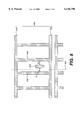
- FIG. 9 is a view illustrating an example of a pixel structure applying an in-plane switching (IPS) mode where pixel electrodes and common electrodes are provided on the same substrate according to the second preferred embodiment of the present invention.
- IPS in-plane switching
- the pixel structure includes horizontal gate lines 510 and a common line 530 disposed parallel to the horizontal gate lines 510.
- a plurality of common electrodes 540 are connected to the common line 530, the common electrodes 540 being formed perpendicular to the common line 530, and pixel electrodes 550 are formed between the common electrodes 540.
- Distances O and O' between the pixel electrodes 550 and adjacent common electrodes 540 are equal, and widths W and W' of the pixel electrodes 550 and the common electrodes 540 are identical.
- a stitch pattern 560 is interposed between the common line 530 and the upper gate line 510.
- a distance N between the gate line 510 and the stitch pattern 560 is equal to a distance N' between the common line 530 and the stitch pattern 560.
- a stitch line 570 is positioned between the gate line 510 and the stitch pattern 530.
- the gate line 510, common electrode 540, pixel electrode 550, common line 530 and stitch pattern 560 are all formed on a first layer of the pixel structure.
- An insulation layer (not shown) is formed on the first layer, and contact holes 555 are formed at each of the pixel electrodes 550 for exposing the same.
- semiconductor layers are provided on the insulation layer, the semiconductor layers being formed centering around and on both sides of gate electrodes (not shown) of the gate lines 510.
- Data lines 620 are formed on top of the gate insulation layer, the data lines 520 being parallel to the common electrodes 540 and the pixel electrodes 550. Branched from the data lines 520 are source electrodes 522 formed over one of the semiconductor layers, and provided over the other semiconductor layers are drain electrodes 524.
- the gate electrodes, source electrodes 522, drain electrodes 524 and semiconductor layers comprise thin film transistors (TFTs) 515.
- Errors between adjacent panel shots in the IPS mode pixel electrode structure above are measured using the following method.
- a first vertical stitch line 580 is positioned between one pixel electrode 550 and one common electrode 540.
- the pixel structure of FIG. 9 is designed such that the distances O and O' between the pixel electrodes 550 and the adjacent common electrodes 540 are equal, stitch errors are measured by the difference in the distance O and O'.
- a second vertical stitch line 590 is positioned running along the middle of one of the common electrodes 540 (or one of the pixel electrodes 550).
- the width W' of the pixel electrodes 550 and the common electrodes 540, respectively, are designed to be equal
- the width W' of the common electrode 540, the middle of which the second vertical stitch line 590 is formed must be equal to the width W of the pixel electrode 550, through which a stitch line is not formed. Accordingly, a difference between the width W and the width W' after adjacent panel shots have been exposed is indicative of stitch errors, and the degree of the error is determined by subtracting the two widths W and W'.
- stitch errors can be precisely measured using the stitch patterns formed in the active area of the LCD panel even when a shifting, a rotation, a distortion and other flaws occur in the mask manufacturing and installation processes.
- the size of the mask shot can be enlarged such that the total number of exposure is reduced, thereby decreasing the overall exposure time.
- stitch errors can be precisely measured even when a shifting, a rotation, a distortion and other flaws occur in the mask manufacturing and installation processes.
Abstract
Description
Claims (24)
Applications Claiming Priority (2)
| Application Number | Priority Date | Filing Date | Title |
|---|---|---|---|
| KR1019970065084A KR100502797B1 (en) | 1997-12-01 | 1997-12-01 | Liquid crystal display device and manufacturing method thereof |
| KR97-65084 | 1997-12-01 |
Publications (1)
| Publication Number | Publication Date |
|---|---|
| US6146796A true US6146796A (en) | 2000-11-14 |
Family
ID=19526177
Family Applications (1)
| Application Number | Title | Priority Date | Filing Date |
|---|---|---|---|
| US09/201,837 Expired - Lifetime US6146796A (en) | 1997-12-01 | 1998-12-01 | Liquid crystal display and a manufacturing method thereof |
Country Status (2)
| Country | Link |
|---|---|
| US (1) | US6146796A (en) |
| KR (1) | KR100502797B1 (en) |
Cited By (15)
| Publication number | Priority date | Publication date | Assignee | Title |
|---|---|---|---|---|
| US6255130B1 (en) * | 1998-11-19 | 2001-07-03 | Samsung Electronics Co., Ltd. | Thin film transistor array panel and a method for manufacturing the same |
| US20030002000A1 (en) * | 2001-07-02 | 2003-01-02 | Nec Corporation | In-plane switching mode liquid crystal display device and method of fabricating the same |
| GB2383140A (en) * | 2001-12-13 | 2003-06-18 | Zarlink Semiconductor Ltd | Exposure positioning in photolithography |
| US20040100605A1 (en) * | 2002-11-19 | 2004-05-27 | Nec Lcd Technologies, Ltd. | Liquid crystal display device and method of fabricating the same |
| US20040141099A1 (en) * | 1997-10-18 | 2004-07-22 | Kim Sang-Soo | Liquid crystal display |
| US6950164B2 (en) * | 2000-12-20 | 2005-09-27 | Lg.Philips Lcd Co., Ltd. | Array substrate for IPS mode liquid crystal display device and method for fabricating the same |
| US20060057788A1 (en) * | 2004-09-13 | 2006-03-16 | Lg Philips Lcd Co., Ltd. | Exposure mask pattern for LCD and exposure method using the same |
| US20060204863A1 (en) * | 2002-10-10 | 2006-09-14 | Nec Lcd Technologies, Ltd. | Mask for light exposure |
| CN100357831C (en) * | 2001-12-14 | 2007-12-26 | 三星电子株式会社 | Manufacturing method of a panel for liquid crystal display |
| US20080276813A1 (en) * | 2003-12-09 | 2008-11-13 | Koninklijke Phillips Electronic, N.V. | Method and Apparatus for Printing a Patterned Layer on a Flatsubstate with a Flat-Type-Bed |
| US20090244466A1 (en) * | 2008-04-01 | 2009-10-01 | Hitachi Displays, Ltd. | Liquid Crystal Display Device |
| US20130221515A1 (en) * | 2012-02-29 | 2013-08-29 | Canon Kabushiki Kaisha | Semiconductor device and method of manufacturing the same |
| US20140141558A1 (en) * | 2011-09-02 | 2014-05-22 | Panasonic Corporation | Method of manufacturing display panel |
| US10317723B2 (en) * | 2015-04-10 | 2019-06-11 | Samsung Display Co., Ltd | Liquid crystal display and method for manufacturing the same |
| US10809627B2 (en) * | 2018-01-16 | 2020-10-20 | Samsung Display Co., Ltd. | Mask, related display device, and related exposure method for manufacturing display device |
Families Citing this family (4)
| Publication number | Priority date | Publication date | Assignee | Title |
|---|---|---|---|---|
| JP4718712B2 (en) * | 2001-04-17 | 2011-07-06 | Nec液晶テクノロジー株式会社 | Active matrix liquid crystal display device |
| KR100499567B1 (en) * | 2001-12-28 | 2005-07-07 | 엘지.필립스 엘시디 주식회사 | Liquid crystal display device and method for manufacturing the same |
| KR100840322B1 (en) * | 2002-02-19 | 2008-06-20 | 삼성전자주식회사 | A manufacturing method of liquid crystal display |
| KR100785190B1 (en) * | 2006-04-06 | 2007-12-11 | 비오이 하이디스 테크놀로지 주식회사 | Monitoring method for stitch |
Citations (6)
| Publication number | Priority date | Publication date | Assignee | Title |
|---|---|---|---|---|
| US5026143A (en) * | 1985-02-06 | 1991-06-25 | Sharp Kabushiki Kaisha | Active type liquid crystal matrix display having signal electrodes with expanded sections at group exposure boundaries |
| US5285302A (en) * | 1992-03-30 | 1994-02-08 | Industrial Technology Research Institute | TFT matrix liquid crystal display with compensation capacitance plus TFT stray capacitance constant irrespective of mask misalignment during patterning |
| US5298761A (en) * | 1991-06-17 | 1994-03-29 | Nikon Corporation | Method and apparatus for exposure process |
| US5656526A (en) * | 1993-12-07 | 1997-08-12 | Kabushiki Kaisha Toshiba | Method of fabricating a display device |
| US5795686A (en) * | 1995-12-26 | 1998-08-18 | Fujitsu Limited | Pattern forming method and method of manufacturing liquid crystal display device |
| US5945256A (en) * | 1997-12-06 | 1999-08-31 | Samsung Electronics Co., Ltd. | Exposing methods in photolithography used for manufacturing a liquid crystal display |
Family Cites Families (4)
| Publication number | Priority date | Publication date | Assignee | Title |
|---|---|---|---|---|
| JP2664551B2 (en) * | 1991-04-03 | 1997-10-15 | シャープ株式会社 | Wiring board exposure processing method |
| JP3224041B2 (en) * | 1992-07-29 | 2001-10-29 | 株式会社ニコン | Exposure method and apparatus |
| JPH0869958A (en) * | 1994-08-30 | 1996-03-12 | Canon Inc | Method and device for manufacturing x-ray mask |
| JPH09127546A (en) * | 1995-11-06 | 1997-05-16 | Advanced Display:Kk | Liquid crystal display element and its production |
-
1997
- 1997-12-01 KR KR1019970065084A patent/KR100502797B1/en not_active IP Right Cessation
-
1998
- 1998-12-01 US US09/201,837 patent/US6146796A/en not_active Expired - Lifetime
Patent Citations (6)
| Publication number | Priority date | Publication date | Assignee | Title |
|---|---|---|---|---|
| US5026143A (en) * | 1985-02-06 | 1991-06-25 | Sharp Kabushiki Kaisha | Active type liquid crystal matrix display having signal electrodes with expanded sections at group exposure boundaries |
| US5298761A (en) * | 1991-06-17 | 1994-03-29 | Nikon Corporation | Method and apparatus for exposure process |
| US5285302A (en) * | 1992-03-30 | 1994-02-08 | Industrial Technology Research Institute | TFT matrix liquid crystal display with compensation capacitance plus TFT stray capacitance constant irrespective of mask misalignment during patterning |
| US5656526A (en) * | 1993-12-07 | 1997-08-12 | Kabushiki Kaisha Toshiba | Method of fabricating a display device |
| US5795686A (en) * | 1995-12-26 | 1998-08-18 | Fujitsu Limited | Pattern forming method and method of manufacturing liquid crystal display device |
| US5945256A (en) * | 1997-12-06 | 1999-08-31 | Samsung Electronics Co., Ltd. | Exposing methods in photolithography used for manufacturing a liquid crystal display |
Cited By (31)
| Publication number | Priority date | Publication date | Assignee | Title |
|---|---|---|---|---|
| US7463323B2 (en) * | 1997-10-18 | 2008-12-09 | Samsung Electronics Co., Ltd. | Liquid crystal display |
| US20040141099A1 (en) * | 1997-10-18 | 2004-07-22 | Kim Sang-Soo | Liquid crystal display |
| US6255130B1 (en) * | 1998-11-19 | 2001-07-03 | Samsung Electronics Co., Ltd. | Thin film transistor array panel and a method for manufacturing the same |
| US6950164B2 (en) * | 2000-12-20 | 2005-09-27 | Lg.Philips Lcd Co., Ltd. | Array substrate for IPS mode liquid crystal display device and method for fabricating the same |
| US6762814B2 (en) * | 2001-07-02 | 2004-07-13 | Nec Lcd Technologies, Ltd. | In-plane switching mode liquid crystal display device and method of fabricating the same |
| US20030002000A1 (en) * | 2001-07-02 | 2003-01-02 | Nec Corporation | In-plane switching mode liquid crystal display device and method of fabricating the same |
| US20030124439A1 (en) * | 2001-12-13 | 2003-07-03 | Brian Martin | Exposure positioning in photolithography |
| EP1319985A2 (en) * | 2001-12-13 | 2003-06-18 | Zarlink Semiconductor Limited | Reticle |
| EP1319985A3 (en) * | 2001-12-13 | 2005-03-16 | Zarlink Semiconductor Limited | Reticle |
| GB2383140A (en) * | 2001-12-13 | 2003-06-18 | Zarlink Semiconductor Ltd | Exposure positioning in photolithography |
| US6962762B2 (en) | 2001-12-13 | 2005-11-08 | Zarlink Semiconductor Limited | Exposure positioning in photolithography |
| CN100357831C (en) * | 2001-12-14 | 2007-12-26 | 三星电子株式会社 | Manufacturing method of a panel for liquid crystal display |
| US7803501B2 (en) * | 2002-10-10 | 2010-09-28 | Nec Lcd Technologies, Ltd. | Mask for light exposure |
| US20060204863A1 (en) * | 2002-10-10 | 2006-09-14 | Nec Lcd Technologies, Ltd. | Mask for light exposure |
| US20060209249A1 (en) * | 2002-11-19 | 2006-09-21 | Nec Lcd Technologies, Ltd | Liquid crystal display device and method of fabricating the same |
| US20040100605A1 (en) * | 2002-11-19 | 2004-05-27 | Nec Lcd Technologies, Ltd. | Liquid crystal display device and method of fabricating the same |
| US20060209234A1 (en) * | 2002-11-19 | 2006-09-21 | Nec Lcd Technologies, Ltd | Liquid crystal display device and method of fabricating the same |
| US7388644B2 (en) | 2002-11-19 | 2008-06-17 | Nec Lcd Technologies, Ltd. | Liquid crystal display device and method of fabricating the same |
| US7405782B2 (en) | 2002-11-19 | 2008-07-29 | Nec Lcd Technologies, Ltd. | Liquid crystal display device and method fabricating the same |
| US7136120B2 (en) * | 2002-11-19 | 2006-11-14 | Nec Lcd Technologies, Ltd. | Liquid crystal display device and method of fabricating the same |
| US20080276813A1 (en) * | 2003-12-09 | 2008-11-13 | Koninklijke Phillips Electronic, N.V. | Method and Apparatus for Printing a Patterned Layer on a Flatsubstate with a Flat-Type-Bed |
| US7674572B2 (en) * | 2004-09-13 | 2010-03-09 | Lg. Display Co., Ltd. | Exposure mask pattern for LCD and exposure method using the same |
| US20060057788A1 (en) * | 2004-09-13 | 2006-03-16 | Lg Philips Lcd Co., Ltd. | Exposure mask pattern for LCD and exposure method using the same |
| US20090244466A1 (en) * | 2008-04-01 | 2009-10-01 | Hitachi Displays, Ltd. | Liquid Crystal Display Device |
| US20140141558A1 (en) * | 2011-09-02 | 2014-05-22 | Panasonic Corporation | Method of manufacturing display panel |
| US9245930B2 (en) * | 2011-09-02 | 2016-01-26 | Joled Inc. | Method of manufacturing display panel |
| US20130221515A1 (en) * | 2012-02-29 | 2013-08-29 | Canon Kabushiki Kaisha | Semiconductor device and method of manufacturing the same |
| JP2013182942A (en) * | 2012-02-29 | 2013-09-12 | Canon Inc | Semiconductor device and manufacturing method therefor |
| US9081284B2 (en) * | 2012-02-29 | 2015-07-14 | Canon Kabushiki Kaisha | Method of manufacturing forming conductive line pattern in boundary region |
| US10317723B2 (en) * | 2015-04-10 | 2019-06-11 | Samsung Display Co., Ltd | Liquid crystal display and method for manufacturing the same |
| US10809627B2 (en) * | 2018-01-16 | 2020-10-20 | Samsung Display Co., Ltd. | Mask, related display device, and related exposure method for manufacturing display device |
Also Published As
| Publication number | Publication date |
|---|---|
| KR19990046917A (en) | 1999-07-05 |
| KR100502797B1 (en) | 2005-10-19 |
Similar Documents
| Publication | Publication Date | Title |
|---|---|---|
| US6146796A (en) | Liquid crystal display and a manufacturing method thereof | |
| US8023092B2 (en) | Liquid crystal display device and method of manufacturing liquid crystal display device | |
| JP2010092072A (en) | Color filter substrate for liquid crystal display device, thin film transistor substrate, and method for manufacturing them | |
| JP2004361949A (en) | Thin film transistor display plate and liquid crystal display device including the same | |
| KR100315911B1 (en) | Liquid crystal display panel, method for fabricating the same and method for aligning the same | |
| KR20090034579A (en) | Thin film transistor array panel and manufacturung method thereof | |
| US6972819B2 (en) | Method of manufacturing IPS-LCD using 4-mask process | |
| KR100947538B1 (en) | Method Of Exposing And Method of Manufacturing Thin Film Transistor Of Liquid Crystal Display Device | |
| US7279257B2 (en) | Pattern forming method, method of manufacturing thin film transistor substrate, method of manufacturing liquid crystal display and exposure mask | |
| TW543199B (en) | Method for forming pattern on substrate and method for fabricating liquid crystal display using the same | |
| WO2006059693A1 (en) | Method for manufacturing display and display | |
| US7189496B2 (en) | Method for the manufacture of an active matrix, corresponding electro-optical display devices and mask | |
| KR100529575B1 (en) | Substrate manufacturing method of liquid crystal display device | |
| CN111290658B (en) | Array substrate, preparation method thereof and touch display panel | |
| KR100658123B1 (en) | Pattern forming method, method for manufacturing matrix substrate of thin film transistor, and light exposure mask | |
| JPH0829809A (en) | Thin film transistor and its production | |
| KR20130031738A (en) | Liquid crystal display device and method for fabrciating the same | |
| KR100840322B1 (en) | A manufacturing method of liquid crystal display | |
| KR100268313B1 (en) | Mask for isolating semiconductor device and manufacturing mathod of the semiconductor device using the mask | |
| KR100577775B1 (en) | Method for fabricating thin film transistor array substrate | |
| KR19980016214A (en) | Manufacturing method of liquid crystal display device | |
| KR20160083348A (en) | Method of fabricating array substrate for liquid crystal display device | |
| KR20020056111A (en) | array panel of liquid crystal display and manufacturing method thereof | |
| KR20030050577A (en) | liquid crystal display, color filter plate and method for fabricating the plate | |
| JP2007213075A (en) | Method for manufacturing thin film transistor substrate, and thin film transistor substrate and display panel having the same |
Legal Events
| Date | Code | Title | Description |
|---|---|---|---|
| AS | Assignment |
Owner name: SAMSUNG ELECTRONICS CO., LTD., KOREA, REPUBLIC OF Free format text: ASSIGNMENT OF ASSIGNORS INTEREST;ASSIGNOR:KIM, DONG-GYU;REEL/FRAME:009649/0667 Effective date: 19981201 |
|
| STCF | Information on status: patent grant |
Free format text: PATENTED CASE |
|
| FEPP | Fee payment procedure |
Free format text: PAYOR NUMBER ASSIGNED (ORIGINAL EVENT CODE: ASPN); ENTITY STATUS OF PATENT OWNER: LARGE ENTITY |
|
| FPAY | Fee payment |
Year of fee payment: 4 |
|
| FPAY | Fee payment |
Year of fee payment: 8 |
|
| FEPP | Fee payment procedure |
Free format text: PAYOR NUMBER ASSIGNED (ORIGINAL EVENT CODE: ASPN); ENTITY STATUS OF PATENT OWNER: LARGE ENTITY Free format text: PAYER NUMBER DE-ASSIGNED (ORIGINAL EVENT CODE: RMPN); ENTITY STATUS OF PATENT OWNER: LARGE ENTITY |
|
| FPAY | Fee payment |
Year of fee payment: 12 |
|
| AS | Assignment |
Owner name: SAMSUNG DISPLAY CO., LTD., KOREA, REPUBLIC OF Free format text: ASSIGNMENT OF ASSIGNORS INTEREST;ASSIGNOR:SAMSUNG ELECTRONICS CO., LTD.;REEL/FRAME:029008/0669 Effective date: 20120904 |