US6126775A - Method of microfabrication - Google Patents
Method of microfabrication Download PDFInfo
- Publication number
- US6126775A US6126775A US09/228,659 US22865999A US6126775A US 6126775 A US6126775 A US 6126775A US 22865999 A US22865999 A US 22865999A US 6126775 A US6126775 A US 6126775A
- Authority
- US
- United States
- Prior art keywords
- array
- optical
- temperature
- polarization
- fixtures
- Prior art date
- Legal status (The legal status is an assumption and is not a legal conclusion. Google has not performed a legal analysis and makes no representation as to the accuracy of the status listed.)
- Expired - Fee Related
Links
- 238000000034 method Methods 0.000 title claims abstract description 61
- 230000003287 optical effect Effects 0.000 claims abstract description 180
- 238000000429 assembly Methods 0.000 claims abstract description 43
- 230000000712 assembly Effects 0.000 claims abstract description 33
- 238000004519 manufacturing process Methods 0.000 claims abstract description 31
- 238000003475 lamination Methods 0.000 claims abstract description 14
- 238000003466 welding Methods 0.000 claims description 12
- 238000004080 punching Methods 0.000 claims description 10
- 238000010008 shearing Methods 0.000 claims description 10
- 238000010030 laminating Methods 0.000 claims description 9
- 238000004026 adhesive bonding Methods 0.000 claims description 7
- 238000003491 array Methods 0.000 claims description 7
- 238000005219 brazing Methods 0.000 claims description 6
- 238000000465 moulding Methods 0.000 claims description 3
- 238000005304 joining Methods 0.000 claims 3
- 238000005530 etching Methods 0.000 claims 2
- 230000010287 polarization Effects 0.000 abstract description 150
- 238000002955 isolation Methods 0.000 abstract description 63
- 230000006903 response to temperature Effects 0.000 abstract description 2
- 230000005540 biological transmission Effects 0.000 description 35
- 230000000694 effects Effects 0.000 description 23
- 239000000463 material Substances 0.000 description 15
- 230000008901 benefit Effects 0.000 description 14
- 230000000903 blocking effect Effects 0.000 description 14
- 239000004593 Epoxy Substances 0.000 description 13
- 230000001419 dependent effect Effects 0.000 description 13
- 238000013461 design Methods 0.000 description 10
- 239000002184 metal Substances 0.000 description 8
- 229910052751 metal Inorganic materials 0.000 description 8
- PXHVJJICTQNCMI-UHFFFAOYSA-N Nickel Chemical compound [Ni] PXHVJJICTQNCMI-UHFFFAOYSA-N 0.000 description 7
- 238000005476 soldering Methods 0.000 description 7
- 230000008859 change Effects 0.000 description 6
- 238000003754 machining Methods 0.000 description 6
- 230000015556 catabolic process Effects 0.000 description 5
- 238000006731 degradation reaction Methods 0.000 description 5
- 229910045601 alloy Inorganic materials 0.000 description 4
- 239000000956 alloy Substances 0.000 description 4
- 238000010276 construction Methods 0.000 description 4
- 239000010949 copper Substances 0.000 description 4
- 230000007423 decrease Effects 0.000 description 4
- 239000013307 optical fiber Substances 0.000 description 4
- 239000004033 plastic Substances 0.000 description 4
- 229920003023 plastic Polymers 0.000 description 4
- 239000010935 stainless steel Substances 0.000 description 4
- 229910001220 stainless steel Inorganic materials 0.000 description 4
- RYGMFSIKBFXOCR-UHFFFAOYSA-N Copper Chemical compound [Cu] RYGMFSIKBFXOCR-UHFFFAOYSA-N 0.000 description 3
- 239000000919 ceramic Substances 0.000 description 3
- 230000008602 contraction Effects 0.000 description 3
- 238000001816 cooling Methods 0.000 description 3
- 229910052802 copper Inorganic materials 0.000 description 3
- 239000013078 crystal Substances 0.000 description 3
- 239000000835 fiber Substances 0.000 description 3
- 239000003292 glue Substances 0.000 description 3
- 238000010438 heat treatment Methods 0.000 description 3
- 230000006872 improvement Effects 0.000 description 3
- 150000002739 metals Chemical class 0.000 description 3
- 239000000203 mixture Substances 0.000 description 3
- 229910052759 nickel Inorganic materials 0.000 description 3
- 238000007747 plating Methods 0.000 description 3
- 239000000126 substance Substances 0.000 description 3
- 238000009966 trimming Methods 0.000 description 3
- 239000004696 Poly ether ether ketone Substances 0.000 description 2
- 238000013459 approach Methods 0.000 description 2
- 238000005266 casting Methods 0.000 description 2
- 238000004891 communication Methods 0.000 description 2
- 238000012937 correction Methods 0.000 description 2
- 238000009713 electroplating Methods 0.000 description 2
- 229920006351 engineering plastic Polymers 0.000 description 2
- 238000005516 engineering process Methods 0.000 description 2
- 230000002708 enhancing effect Effects 0.000 description 2
- 238000005242 forging Methods 0.000 description 2
- 239000002223 garnet Substances 0.000 description 2
- 230000005693 optoelectronics Effects 0.000 description 2
- 238000001259 photo etching Methods 0.000 description 2
- 229920002530 polyetherether ketone Polymers 0.000 description 2
- 229910000679 solder Inorganic materials 0.000 description 2
- 238000012360 testing method Methods 0.000 description 2
- VYZAMTAEIAYCRO-UHFFFAOYSA-N Chromium Chemical compound [Cr] VYZAMTAEIAYCRO-UHFFFAOYSA-N 0.000 description 1
- 229910001374 Invar Inorganic materials 0.000 description 1
- 239000004677 Nylon Substances 0.000 description 1
- BQCADISMDOOEFD-UHFFFAOYSA-N Silver Chemical compound [Ag] BQCADISMDOOEFD-UHFFFAOYSA-N 0.000 description 1
- 239000004809 Teflon Substances 0.000 description 1
- 229920006362 Teflon® Polymers 0.000 description 1
- 238000004458 analytical method Methods 0.000 description 1
- 230000003542 behavioural effect Effects 0.000 description 1
- 238000009529 body temperature measurement Methods 0.000 description 1
- 229910052804 chromium Inorganic materials 0.000 description 1
- 239000011651 chromium Substances 0.000 description 1
- 239000011248 coating agent Substances 0.000 description 1
- 238000000576 coating method Methods 0.000 description 1
- 238000005260 corrosion Methods 0.000 description 1
- 230000007797 corrosion Effects 0.000 description 1
- 230000000593 degrading effect Effects 0.000 description 1
- 230000001627 detrimental effect Effects 0.000 description 1
- 238000006073 displacement reaction Methods 0.000 description 1
- 238000001035 drying Methods 0.000 description 1
- 238000005323 electroforming Methods 0.000 description 1
- 229920006332 epoxy adhesive Polymers 0.000 description 1
- 239000011521 glass Substances 0.000 description 1
- PCHJSUWPFVWCPO-UHFFFAOYSA-N gold Chemical compound [Au] PCHJSUWPFVWCPO-UHFFFAOYSA-N 0.000 description 1
- 229910052737 gold Inorganic materials 0.000 description 1
- 239000010931 gold Substances 0.000 description 1
- 239000007769 metal material Substances 0.000 description 1
- 150000002815 nickel Chemical class 0.000 description 1
- 229920001778 nylon Polymers 0.000 description 1
- ISWSIDIOOBJBQZ-UHFFFAOYSA-N phenol group Chemical group C1(=CC=CC=C1)O ISWSIDIOOBJBQZ-UHFFFAOYSA-N 0.000 description 1
- 230000008569 process Effects 0.000 description 1
- 230000001902 propagating effect Effects 0.000 description 1
- 230000004044 response Effects 0.000 description 1
- 239000004065 semiconductor Substances 0.000 description 1
- 229910052709 silver Inorganic materials 0.000 description 1
- 239000004332 silver Substances 0.000 description 1
- 239000000758 substrate Substances 0.000 description 1
- 238000001771 vacuum deposition Methods 0.000 description 1
Images


Classifications
-
- G—PHYSICS
- G02—OPTICS
- G02B—OPTICAL ELEMENTS, SYSTEMS OR APPARATUS
- G02B27/00—Optical systems or apparatus not provided for by any of the groups G02B1/00 - G02B26/00, G02B30/00
- G02B27/62—Optical apparatus specially adapted for adjusting optical elements during the assembly of optical systems
-
- B—PERFORMING OPERATIONS; TRANSPORTING
- B29—WORKING OF PLASTICS; WORKING OF SUBSTANCES IN A PLASTIC STATE IN GENERAL
- B29D—PRODUCING PARTICULAR ARTICLES FROM PLASTICS OR FROM SUBSTANCES IN A PLASTIC STATE
- B29D11/00—Producing optical elements, e.g. lenses or prisms
- B29D11/0073—Optical laminates
-
- G—PHYSICS
- G02—OPTICS
- G02B—OPTICAL ELEMENTS, SYSTEMS OR APPARATUS
- G02B7/00—Mountings, adjusting means, or light-tight connections, for optical elements
-
- G—PHYSICS
- G02—OPTICS
- G02F—OPTICAL DEVICES OR ARRANGEMENTS FOR THE CONTROL OF LIGHT BY MODIFICATION OF THE OPTICAL PROPERTIES OF THE MEDIA OF THE ELEMENTS INVOLVED THEREIN; NON-LINEAR OPTICS; FREQUENCY-CHANGING OF LIGHT; OPTICAL LOGIC ELEMENTS; OPTICAL ANALOGUE/DIGITAL CONVERTERS
- G02F1/00—Devices or arrangements for the control of the intensity, colour, phase, polarisation or direction of light arriving from an independent light source, e.g. switching, gating or modulating; Non-linear optics
- G02F1/01—Devices or arrangements for the control of the intensity, colour, phase, polarisation or direction of light arriving from an independent light source, e.g. switching, gating or modulating; Non-linear optics for the control of the intensity, phase, polarisation or colour
- G02F1/09—Devices or arrangements for the control of the intensity, colour, phase, polarisation or direction of light arriving from an independent light source, e.g. switching, gating or modulating; Non-linear optics for the control of the intensity, phase, polarisation or colour based on magneto-optical elements, e.g. exhibiting Faraday effect
- G02F1/093—Devices or arrangements for the control of the intensity, colour, phase, polarisation or direction of light arriving from an independent light source, e.g. switching, gating or modulating; Non-linear optics for the control of the intensity, phase, polarisation or colour based on magneto-optical elements, e.g. exhibiting Faraday effect used as non-reciprocal devices, e.g. optical isolators, circulators
-
- Y—GENERAL TAGGING OF NEW TECHNOLOGICAL DEVELOPMENTS; GENERAL TAGGING OF CROSS-SECTIONAL TECHNOLOGIES SPANNING OVER SEVERAL SECTIONS OF THE IPC; TECHNICAL SUBJECTS COVERED BY FORMER USPC CROSS-REFERENCE ART COLLECTIONS [XRACs] AND DIGESTS
- Y10—TECHNICAL SUBJECTS COVERED BY FORMER USPC
- Y10S—TECHNICAL SUBJECTS COVERED BY FORMER USPC CROSS-REFERENCE ART COLLECTIONS [XRACs] AND DIGESTS
- Y10S359/00—Optical: systems and elements
- Y10S359/90—Methods
-
- Y—GENERAL TAGGING OF NEW TECHNOLOGICAL DEVELOPMENTS; GENERAL TAGGING OF CROSS-SECTIONAL TECHNOLOGIES SPANNING OVER SEVERAL SECTIONS OF THE IPC; TECHNICAL SUBJECTS COVERED BY FORMER USPC CROSS-REFERENCE ART COLLECTIONS [XRACs] AND DIGESTS
- Y10—TECHNICAL SUBJECTS COVERED BY FORMER USPC
- Y10T—TECHNICAL SUBJECTS COVERED BY FORMER US CLASSIFICATION
- Y10T156/00—Adhesive bonding and miscellaneous chemical manufacture
- Y10T156/10—Methods of surface bonding and/or assembly therefor
- Y10T156/1052—Methods of surface bonding and/or assembly therefor with cutting, punching, tearing or severing
-
- Y—GENERAL TAGGING OF NEW TECHNOLOGICAL DEVELOPMENTS; GENERAL TAGGING OF CROSS-SECTIONAL TECHNOLOGIES SPANNING OVER SEVERAL SECTIONS OF THE IPC; TECHNICAL SUBJECTS COVERED BY FORMER USPC CROSS-REFERENCE ART COLLECTIONS [XRACs] AND DIGESTS
- Y10—TECHNICAL SUBJECTS COVERED BY FORMER USPC
- Y10T—TECHNICAL SUBJECTS COVERED BY FORMER US CLASSIFICATION
- Y10T156/00—Adhesive bonding and miscellaneous chemical manufacture
- Y10T156/10—Methods of surface bonding and/or assembly therefor
- Y10T156/1089—Methods of surface bonding and/or assembly therefor of discrete laminae to single face of additional lamina
- Y10T156/1092—All laminae planar and face to face
Definitions
- the present invention relates generally to optical devices and, in particular, to a temperature compensator for a Faraday rotator and a lamination-based method for manufacturing of optical assemblies and other small components.
- an optical isolator as described for instance in Bellcore's Special Report, Optical Isolators: Reliability Issues, SR-NWT-002855, Issue 1, December 1993, Pages 1-3, incorporated herein by reference, may be used.
- This is an example of an optical device that allows light to propagate (with relatively low loss) in one direction but isolates reflected light from propagating in the reverse direction.
- Optical isolators are used to improve the performance of many devices such as external modulators, distributed feedback lasers, Fabry-Perot lasers, semiconductor amplifiers, and diode-pumped solid-state lasers among others.
- Optical isolators are typically passive, non-reciprocal optical devices based on the Faraday effect.
- Michael Faraday discovered that the plane of polarized light rotates while transmitting through glass which is contained in a magnetic field.
- the Faraday effect is non-reciprocal, meaning that the direction of rotation is independent of the direction of light propagation, and only dependent upon the direction of the magnetic field.
- Most commercial optical isolators utilize this effect to isolate various parts of an optical communication system from reflection-induced noise.
- an optical isolator consists of a magneto-optical material called a Faraday rotator which is sandwiched between a pair of polarization elements commonly referred to as a polarizer and an analyzer.
- the Faraday rotator is used in optical devices, such as the optical isolator, to rotate the plane of polarization that is incident upon it by a predetermined amount, usually by 45° either clockwise or counter clockwise.
- the Faraday rotator is a garnet crystalline structure with an inherent magnetic field, so that the direction of Faraday rotation is predetermined. In some cases an external magnetic field may be needed to activate the Faraday rotator.
- the direction of Faraday rotation is dependent on the orientation of the magnetic field but not on the direction of light propagation.
- the Faraday rotator is essential to many devices that utilize its properties in combination with reciprocal polarization elements.
- the optical isolator In the blocking (reverse) direction, reflected light of arbitrary polarization is incident on the analyzer which transmits some of this light and polarizes it to match its axis of polarization.
- this polarized reflected light passes through the Faraday rotator its plane of polarization is again rotated by 45°, clockwise or counterclockwise relative to the direction of light travel, as is predetermined.
- the plane of polarization of the reflected light incident on the polarizer is perpendicular to its axis of polarization, and, thus the reflected light is blocked by the polarizer.
- the optical isolator is used to transmit light from a source in the pass (forward) direction and essentially extinguish any reflected light in the blocking (reverse) direction. This extinguishing effect is commonly known as "isolation".
- the magnitude of the rotation of the plane of polarization of light passing through the Faraday rotator depends on several factors, such as, the strength of the magnetic field, the nature of the material that constitutes the rotator, the frequency of the light, the temperature, and other parameters. Since the components in many optical applications utilizing the Faraday effect may be exposed to temperature variations, the rotational temperature dependency of the Faraday rotator limits the use of Faraday rotators in devices which do not provide some form of temperature compensation to prevent or minimize degradation in performance.
- the rotational temperature dependency of a Faraday rotator can be expressed in terms of a temperature coefficient of rotation, C ROT , defined as: ##EQU1## where, ⁇ is the rotation of the plane of polarized light passing through the Faraday rotator, and T is the temperature.
- a typical Faraday rotator may have a temperature coefficient with a magnitude of as much as about 0.10°/° C. which can cause a variation of Faraday rotation of about 12° over a temperature range of about -40° C. to 85° C.
- undesirable rotation of the light can have significant detrimental effects on the performance of an optical device both in terms of forward transmissivity and degree of reverse isolation. But, since isolation (attenuation in the blocking direction) is measured very close to zero, small changes can have orders of magnitude effects on the degree of isolation in terms of the blocking direction transmission of reflected light.
- One proposed solution to this problem is to provide temperature compensation via a cooling/heating source which maintains the temperature of the Faraday rotator, and possibly the temperature of the entire device, including for example, the laser source, at the required value. This would require that the temperature of the Faraday rotator be monitored and the output from the cooling/heating source be adjusted accordingly.
- the components required in such a temperature compensation system would include a cooling/heating source, temperature measurement device, a feedback system, and a power supply among others.
- a temperature compensation scheme not only adds to the complexity and cost of the device, but, also to the size of the optical device which can limit the use of the device in many applications.
- a cascaded isolator such as a double stage isolator, is utilized to compensate for the effects of temperature variance on optical isolators.
- a double stage isolator utilizes a polarizer, a Faraday rotator, an analyzer/polarizer, a second Faraday rotator, and a second analyzer arranged in this sequence. This effectively provides two stages of optical isolators in series.
- one stage is "de-tuned” to an offset temperature above the ambient temperature while the other stage is “de-tuned” to an offset temperature correspondingly below the ambient temperature so as to provide a more broad-band response between the two temperature extremes.
- Optical components such as the polarizer, the Faraday rotator, and the analyzer of a typical optical compensator, are commonly fixed in an assembly or attached to a common substrate.
- the primary approach, in the industry to date, to fixturing optical components involves the implementation of screw-machined barrels or small blocks with counter-bored features machined in.
- the optical components are placed in these machined cavities which typically tend to be small in size (for example, less than 2 mm in diameter).
- the machining process of generally tiny metal fixtures a costly and time consuming operation, but, also the discrete approach of fixing the optical components is generally not suited for mass automation.
- such a method of fixturing optical components is labor intensive and leads to higher manufacturing costs and lower manufacturing efficiency.
- An optical isolator constructed in accordance with one preferred embodiment of the present invention overcomes some or all of the afore-mentioned disadvantages.
- the optical isolator utilizes the expansion/contraction properties of a bimetallic element to compensate for the effect temperature on Faraday rotation.
- the method also employs, in one embodiment, a lamination manufacturing procedure to create an array of optics-receiving micro-fixtures for receiving or forming optical assemblies.
- the present invention provides thermal compensation in devices utilizing magneto-optical materials, such as Faraday rotators, by utilizing the opening and closing arcing motion of coiled bimetallic metal strips due to their expansion/contraction when exposed to temperature variations.
- a polarization element is attached to a bimetallic element which allows correction for temperature induced Faraday rotation.
- the bimetallic element is configured to optimally match the degree of temperature-induced drift in the Faraday rotation with the rotation of the polarization element.
- a temperature compensated optical isolator is provided.
- the optical isolator includes a pair of polarization elements, a Faraday rotator and a bimetallic element.
- One of the polarization elements is an optical polarizer while the other polarization element is an optical analyzer.
- the Faraday rotator is positioned between the polarizer and analyzer.
- the bimetallic element is attached between the analyzer and a base which houses the polarizer, Faraday rotator, analyzer and bimetallic element.
- the bimetallic element of the present invention is configured to optimally conform with the temperature induced changes in Faraday rotation.
- the bimetallic element By rotating the axis of polarization of the analyzer the bimetallic element ensures that any back-reflected light incident on the polarizer has a plane of polarization substantially perpendicular to the polarizer's axis of polarization.
- all or most of the back-reflected light incident on the polarizer will be effectively extinguished, thereby essentially eliminating any temperature-induced degradation in the effective isolation of the optical system.
- the bimetallic element of the present invention can be tailored to meet the particular characteristics of the magneto-optical material and is hence adaptable to a wide variety of situations and applications. This is accomplished by appropriate material selection, configuration and dimensioning of the bimetallic element.
- the bimetallic element has a generally curved portion which generally circumscribes the analyzer.
- other shapes and configurations may also be employed with efficacy, as required or desired, giving due consideration to the goal of optimally enhancing the isolation performance of the optical isolator over a given range of temperatures.
- the bimetallic element can be used to house a variety of polarization elements and to provide temperature compensation in other optical devices.
- the bimetallic element may be used in conjunction with a half-wave plate or it may be used in combination with an external modulator, to achieve some or all of the benefits and advantages disclosed herein.
- the optical isolator of the present invention provides a significant improvement over conventional single stage isolators by essentially eliminating the effects of temperature on isolation. It is effective in maintaining a consistent optical isolation over an extended temperature range thereby, allowing the optical device to function without costly active temperature control.
- the isolator of the present invention also provides several advantages over conventional double-stage or cascaded isolators. Desirably, it is lower in cost, simpler in design, dimensionally smaller, is easier to manufacture, and provides a shorter optical path. This simplicity and compactness render the isolator of the present invention a viable choice for providing temperature compensation in a wide variety of optical devices. The size of the isolator allows it to readily fit into standard optical packages.
- the simple construction of the isolator make it a practically effortless retrofit into conventional opto-electronic packages.
- the isolator of the present invention is environmentally stable and is well suited for the present and future in the field of telecommunications.
- the present invention also prescribes, in accordance with one embodiment, a preferred method of manufacturing sub-assemblies of optical elements, such as in one embodiment the temperature compensated optical isolator.
- the method utilizes lamination or layering of sheets with arrays of micro-frames to form an array of optic-receiving micro-fixtures.
- the micro-frames are, preferably, photo-chemically etched or stamped into the sheets and are supported by tab members.
- Appropriate optical elements are inserted into the micro-fixtures as dictated by the particular application.
- the laminate units or pallets which accommodate the array of optical elements are stacked, aligned and attached to form an array of optical assemblies in a laminate stack.
- a base member may be attached to the optical assemblies to facilitate their mounting.
- the optical assemblies are removed from the laminate stack by conventional trimming methods.
- such a method is well suited for the automated manufacturing of optical assemblies and results in high speed, high volume production, thereby desirably maintaining low manufacturing costs.
- the method can be used in combination with conventional pick-and-place type of robotics.
- the present method provides an improvement over conventional manufacturing of optical assemblies which typically utilizes a laborious, time-consuming and costly machining process.
- the method can be customized to form or assemble a wide variety of optical components and other small components, and is adaptable to a wide range of applications.
- the method may be used to mount lenses, crystals, gratings, filters, fibers and various sub-assemblies, among others.
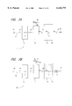
- FIG. 1A is a schematic drawing illustrating the pass-direction operation of a conventional optical isolator, as known in the art
- FIG. 1B is a schematic drawing illustrating the blocking-direction operation of the isolator of FIG. 1A;
- FIG. 2A is a graphical comparison of the theoretical isolation performances, as a function of temperature, between the isolator of FIG. 1 and one preferred embodiment of the isolator of the present invention
- FIG. 2B is a graphical comparison of the theoretical isolation performances, as a function of Faraday rotation, between the isolator of FIG. 1 and one preferred embodiment of the isolator of the present invention
- FIG. 2C is a graphical illustration of the theoretical transmission loss through one preferred embodiment of the isolator of the present invention.
- FIG. 2D is a graphical illustration of the experimental isolation performances, as a function of temperature, between the isolator of FIG. 1 and one preferred embodiment of the isolator of the present invention
- FIG. 3 is a schematic illustration of a temperature compensated optical isolator constructed in accordance with one preferred embodiment of the present invention
- FIG. 4A is a front elevational view illustrating one preferred bimetallic element of the isolator of FIG. 3;
- FIG. 4B is a front elevational view illustrating another preferred bimetallic element of the isolator of FIG. 3;
- FIG. 5 is an exploded perspective view of the isolator of FIG. 3;
- FIG. 6 is a front elevational view illustrating the rotation of the bimetallic element of FIG. 4A;
- FIG. 7A is a schematic drawing illustrating the pass-direction operation of the isolator of FIG. 3, at an optimized temperature
- FIG. 7B is a schematic drawing illustrating the blocking-direction operation of the isolator of FIG. 3, at an optimized temperature
- FIG. 8A is a schematic drawing illustrating the pass-direction operation of the isolator of FIG. 3, at a temperature higher than the optimized temperature;
- FIG. 8B is a schematic drawing illustrating the blocking-direction operation of the isolator of FIG. 3, at a temperature higher than the optimized temperature;
- FIG. 9A is a schematic drawing illustrating the pass-direction operation of the isolator of FIG. 3, at a temperature lower than the optimized temperature;
- FIG. 9B is a schematic drawing illustrating the blocking-direction operation of the isolator of FIG. 3, at a temperature lower than the optimized temperature;
- FIG. 10 is a schematic illustration of the bimetallic element of FIG. 3 in combination with a half-wave plate and a Faraday rotator;
- FIG. 11 is a schematic illustration of a micro-framed sheet in accordance with one preferred embodiment of the method of the present invention.
- FIG. 12A is a front elevational view of one preferred micro-frame of the sheet of FIG. 11;
- FIG. 12B is a front elevational view of another preferred micro-frame of the sheet of FIG. 11;
- FIG. 13 is a front elevational view showing a preferred pair of tab members of the sheet of FIG. 11;
- FIG. 14A is an exploded perspective view illustrating a preferred step of laminating the sheets of FIG. 11;
- FIG. 14B is a perspective view of the laminate unit (pallet) formed by the step of FIG. 14A;
- FIG. 15A is an exploded perspective view of a preferred micro-fixture formed by the step of FIG. 14A;
- FIG. 15B is a perspective view of an assembled micro-fixture formed from the components of FIG. 15A;
- FIG. 15C is a perspective view of the micro-fixture of FIG. 15A in combination with an optical element
- FIG. 15D is a sectional view, taken along line 15D--15D of FIG. 15C;
- FIG. 16A is an exploded perspective view illustrating a preferred step of laminating the laminate units (pallets) of FIG. 14B;
- FIG. 16B is a perspective view of the laminate stack formed by the step of FIG. 16A;
- FIG. 16C is a sectional view, taken along line 16C--16C of FIG. 16B;
- FIG. 17 is a perspective view of a base employed in one preferred embodiment of the method of the present invention.
- FIG. 18 is a front elevational view of another preferred fixture formed by the step of FIG. 14A;
- FIG. 19A is a front elevational view of yet another preferred fixture formed by the step of FIG. 14A.
- FIG. 19B is a sectional view, taken along 19B--19B of FIG. 19A.
- FIGS. 1A and 1B schematically illustrate the operating principle of a conventional optical isolator 10', as is well known in the art.
- the isolator 10' includes a polarizer (polarizing element) 12, a Faraday rotator 14 and an analyzer (polarizing element) 16.
- the optical isolator 10' permits the incident light 18 to be transmitted through it resulting in a beam of transmitted light 20.
- the isolator 10' In the blocking (reverse) direction, as illustrated in FIG. 1B, the isolator 10' ideally blocks all or most of the back-reflected light 22, while operating at the optimized temperature, so that the reflection-induced light 24 passing through the isolator 10' is essentially none or negligible.
- incident light 18 passes through the polarizer 12 without obstruction since its plane of polarization 26 coincides with the axis of polarization of the polarizer 12.
- the back-reflected light 22 of arbitrary polarization 30 is incident on the analyzer 16 which transmits some of this light and polarizes it to a plane of polarization 28 that matches the analyzer axis of polarization.
- the plane of polarization 28 of the reflected light 22 will be oriented at 45° (clockwise) with respect to the plane of polarization 26 of the incident light 18 (FIG. 1A).
- the plane of polarization 32 of the back-reflected light 22 that is transmitted through the Faraday rotator 14 is oriented at 90° with respect to the plane of polarization 26 of the incident light 18 and is, hence, perpendicular to the axis of polarization of the polarizer 12.
- This ideally blocks all or most of the back-reflected light 22 so that the reflection-induced light 24 passing through the polarizer 12 is essentially none or negligible.
- the optical isolator 10' is used to transmit light 18 from a source, such as a laser (not shown) in the pass (forward) direction and essentially extinguish any reflected light 22 in the blocking (reverse) direction.
- isolation is defined as the amount of unpolarized light incident on the analyzer 16 that passes through the polarizer 12.
- the effective transmission, ⁇ , through a polarization element can be defined as:
- k 1 is the maximum transmission of polarized light through the polarizing element
- k 2 is the minimum transmission of polarized light through the polarizing element
- ⁇ is the angular offset between the plane of polarization of the polarized light and the axis of polarization of the polarization element.
- the effective transmission, ⁇ 16 of the unpolarized reflected light 22 with arbitrary polarization 30 through the analyzer 16 is given by:
- the degree or amount of isolation, I, of the optical isolator 10' can also be represented in terms of deciBels (dB) by:
- each Faraday rotator has a temperature coefficient of rotation.
- changes in temperature influence the magnitude of Faraday rotation and can undesirably lead to degradation in isolation performance.
- the temperature of the Faraday rotator (FIGS. 1A and 1B) changes from the optimum operating temperature
- the plane of polarization 32 (FIG. 1B) of the back-reflected light incident on the polarizer 12 will be offset somewhat from the desired 90°. This will result in an increase in the effective transmission ⁇ 12 of reflected light back through the polarizer 12, and hence, an increase in the noise or isolation transmission ⁇ ISO and a corresponding undesirable decrease in the isolation, I, of the optical isolator 10'.
- the graph of FIG. 2A shows the effect of temperature on the isolation with the x-axis 38 representing the temperature and the y-axis 40 representing the amount of isolation, I.
- the isolation of the optical isolator 10' (FIGS. 1A and 1B) is a maximum at the optimum operating temperature of 25° C. But, as the temperature varies from 25° C., the isolation, undesirably, drops sharply.
- a temperature variation of about 70° C. causes a drop of more than 20 dB in the amount of isolation. This represents an almost 150-fold increase in the amount of back-reflected noise, ⁇ ISO , admitted into the optical circuit.
- the graph of FIG. 2B shows a similar effect on the isolation in terms of the rotation, ⁇ , through the Faraday rotator (FIGS. 1A and 1B) with the x-axis 42 representing the Faraday rotation and the y-axis 44 representing the amount of isolation.
- the isolation of the optical isolator 10' (FIGS. 1A and 1B) is a maximum at the optimum Faraday rotation of 45°.
- the isolation undesirably, drops sharply.
- a Faraday rotation variation of about 7° causes a drop of more than 20 dB in the amount of isolation. This represents an almost 150-fold increase in the amount of back-reflected noise ⁇ ISO admitted into the optical circuit.
- the temperature variation will also affect the transmission of light through the isolator 10' in the pass (forward) direction shown in FIG. 1A.
- the transmission in the pass (forward) direction will be reduced since the light incident on the analyzer 16 (FIG. 1A) will have a plane of polarization that is offset from the axis of polarization of the analyzer, due to the temperature induced variation in Faraday rotation.
- This transmission loss in deciBels can be determined by using equation (5), and is typically small.
- temperature variations are critical in undesirably degrading the isolation performance of the prior art optical isolator 10', while having a less significant effect on the forward transmission.
- the present invention provides thermal compensation for magneto-optical materials, such as a Faraday rotator, by utilizing the arcing or curling motion of bimetallic metal strips due to their expansion/contraction when exposed to temperature variations.
- a polarization element is attached to a bimetallic element which allows correction for temperature induced Faraday rotation.
- the bimetallic element is configured to optimally match the Faraday rotation with the polarization element rotation.
- FIG. 3 schematically illustrates one preferred embodiment of a temperature compensated optical isolator 10 including a polarizer or polarization element 12, a magneto-optical element or Faraday rotator 14, and an analyzer or a polarization element 16 which is attached to a bimetallic element 46.
- FIG. 4A is a detailed front view depicting how the analyzer 16 is attached to the bimetallic element 46.
- the bimetallic element will expand or contract causing the analyzer 16 to be rotated in a clockwise or counterclockwise direction.
- the arcing or curling motion of the bimetallic element 46 causes the analyzer 16, and hence its axis of polarization 72, to be rotated about an axis 54 (shown in FIGS. 3, to 6) that is parallel to the direction of propagation of the light incident on the isolator 10 and generally passes through the center of the polarizer 12, Faraday rotator 14 and analyzer 16.
- This rotation is relative to the axis of polarization 74 of the polarizer 12 and is illustrated in FIG. 4A by the position of the analyzers labeled 16a and 16b.
- the axes of polarization 72 and 74 are angularly offset by about 45° and no temperature compensation is required, as discussed above.
- the bimetallic element 46 includes a pair of generally straight portions 48, 52 which are joined by a generally curved portion 50.
- the analyzer 16 is attached to the bimetallic element straight portion 48 such that the bimetallic element 46 generally circumscribes it while allowing the analyzer 16 to freely rotate as the bimetallic element expands or contracts.
- the analyzer 16 is glued to the bimetallic element 46 utilizing pad-printable B-stageable epoxy #118-03 available from Creative Materials Inc. of Tyngsboro, Mass.
- the analyzer 16 may be attached to the bimetallic element 46 using EP353-ND epoxy available from Epoxy Technology of Billerica, Mass,
- EP353-ND epoxy available from Epoxy Technology of Billerica, Mass
- other types of glues or other attachment means such as pins, locks, clamps, soldering or brazing among others, may be used with efficacy to affix the analyzer 16 to the bimetallic element 46 giving due consideration to the desired goal of providing a reliable, clean, inert and generally temperature independent attachment.
- the edge of the analyzer 16 is metallized with layers of chromium, nickel and gold using vacuum deposition. This permits the analyzer 16 to be attached to the bimetallic element 46, as illustrated, for example, in FIG. 5, by soldering.
- the bimetallic element straight portion 52 is attached to a base or support 56.
- the base 56 is generally yoke-shaped with a generally U-shaped cavity 64 in communication with a generally circular cavity 62 for housing the polarizer 12 and Faraday rotator 14.
- the base 56 can be alternately configured as needed or desired, giving due consideration to the goals of providing a support for the isolator 10 and for permitting the isolator 10 to be readily mounted in optical devices.
- the bimetallic element straight portion 52 resides inside the cavity 64 and is attached to an inner surface 60 of a wall 58 of the base 56. The flat surface feature of the inner surface 60 facilitates this attachment.
- the bimetallic element straight portion 52 is laser welded to the base 56, though other attachment means, such as resistance welding, soldering or gluing, for example, using epoxy, may be utilized with efficacy.
- a curved portion 50' of a bimetallic element 46' is attached to a groove 112 in a base wall 58' while a flat portion is affixed to the analyzer 16.
- the polarizer 12 and the Faraday rotator 14 are mounted in fixtures 66 and 68, respectively, using the B-stageable epoxy.
- other types of glues such as the EP353-ND epoxy, or other attachment means, such as pins, locks and clamps among others, may be used with efficacy to affix the polarizer 12 and Faraday rotator 14 to the respective fixtures 66, 68 giving due consideration to the desired goal of providing a reliable, clean, inert and generally temperature independent attachment.
- the polarizer fixture 66 and the Faraday rotator fixture 68 are configured to fit in the generally circular base cavity 62, and define an aperture 70 (see FIG. 4A) through which light can pass.
- the optical isolator 10 is configured so that the entire field of view of the aperture 70 lies within the analyzer 16, even when the analyzer 16 rotates to provide temperature compensation.
- the polarizer fixture 66 and Faraday rotator fixture 68 are laser welded to the base 56, though other attachment means, such as resistance welding, soldering or gluing, for example, using epoxy, may be utilized with efficacy.
- the polarizer fixture 66 and Faraday rotator fixture 68 may also be affixed to one another by one or more of the attachment means discussed above.
- the polarizer 12 and the analyzer 16 are high contrast POLARCORTM polarizing elements with a V2 anti-reflecting coating, and are available from Corning Inc. of Corning, N.Y.
- the particular wavelength or range of wavelengths of the application dictates the selection of the POLARCORTM element.
- the Faraday rotator 14 is a Latching Gamet Film #L22, which in use does not require an external magnetic field. Such devices are available from Lucent Technologies of Murray Hill, N.J. Again, the wavelength selection is dictated by the requirements of the particular application.
- the Faraday rotator may be fabricated from a variety of other magneto-optical materials to achieve the benefits and advantages disclosed herein.
- a non-latching garnet may also be used as the Faraday rotator 14 and the entire isolator assembly housed in a magnet or the magnet may be shaped into a base, such as the base 56.
- the base 56 is preferably fabricated from stainless steel, though other alloys, metals, plastics and ceramics may be utilized with efficacy, as required or desired.
- the base 56 may be manufactured by machining, molding, forging or casting.
- the base 56 may be molded from a high temperature engineering plastic, such as nylon, teflon, polyetheretherketone (PEEK) or phenolic.
- the bimetallic element 46 is fabricated from ASTM #TM2, available from Atlantic Alloys of Bristol, R.I.
- ASTM #TM2 has an inner high expansion side (HES) 47 with a 55% layer ratio and a chemical composition of 72 Mn, 18 Cu, 10 Ni, and an outer low expansion side (LES) 49 with a 45% layer ratio and a chemical composition of 36 Ni, 64 Fe (Invar).
- HES high expansion side
- LES outer low expansion side
- the ASTM #TM2 is nickel plated for corrosion resistance. In one preferred form of the present invention, this nickel plating also permits the analyzer 16 to be soldered to the bimetallic element 46, as indicated above.
- bimetallic element 46 is largely dictated by the temperature range of interest, and by the particular configuration and components of the optical isolator 10 and their behavioral variance characteristics over that temperature range.
- bimetallic elements with alternate layer ratios and chemical compositions may be used with efficacy, as required or desired, giving due consideration to the goal of providing optimal temperature compensation and maximum isolation.
- the angular rotation, A, of the bimetallic element 46 is dependent not only on the material specification of the bimetallic element 46, but also on its active length, L, and thickness, t.
- the angular rotation, A can be approximated by: ##EQU2## where, F is the flexivity of the materials comprising the bimetallic element 46 and ⁇ T is the temperature change or variation from the optimum operational temperature, which is typically 25° C. Desirably, the angular rotation, A, is linearly dependent on the temperature change, ⁇ T, as can be seen from equation (6).
- the temperature coefficient of rotation, C ROT of most Faraday rotator's remains approximately constant as a function of temperature, that is, the change in Faraday rotation is approximately linearly dependent on the temperature change.
- this permits, by proper selection of the material and dimensions of the bimetallic element 46, the temperature induced change in Faraday rotation to be matched by a generally corresponding angular rotation of the bimetallic element 46.
- the analyzer 16 which is attached to the bimetallic element 46, as shown in FIG. 4A, undergoes a corresponding rotation which substantially compensates for undesirable thermally induced back-reflection, as will be discussed at greater length later herein.
- the optical isolator 10 (shown, for example, in FIG. 5) is dimensioned and configured to optimally compensate for temperature variations in the range of -40° C. (-40° F.) to 85° C. (185° F.).
- the bimetallic element 46 is ASTM #TM2 as discussed above and its average flexivity is approximately 186 ⁇ 10 -7 mm/mm/° C. (203 ⁇ 10 -7 in/in/° F.) in the above temperature range of interest.
- the flexivity value will also have some temperature dependency. But, advantageously, the deviation in flexivity of ASTM #TM2 from the average value is small. In the above temperature range the flexivity value changes in the range from about +1% to about -6%.
- the optical isolator 10 is configured so that the respective axes of polarizations 74, 72 of the polarizer 12 and analyzer 16 are angularly offset by 45° at a desired nominal design temperature, such as 25° C.
- a desired nominal design temperature such as 25° C.
- the analyzer 16 and the bimetallic element 46 are positioned as illustrated in FIGS. 4A and 6.
- the curved portion 50 of the bimetallic element 46 defines an included angle of about 218° and has an internal diameter of about 1.905 mm (0.075 inches).
- the thickness of the bimetallic element is about 0.1016 mm (0.004 inches) and its width is about 0.7874 mm (0.031 inches). With these dimensions, the active length, L, of the bimetallic element 46 is readily calculated to be about 3.81 mm (0.150 inches).
- the bimetallic element 46 curls outwards or expands as illustrated by the position of the bimetallic element 46a.
- equation (6) at the upper temperature extreme of 85° C. (185° F.), the bimetallic element 46 will undergo an angular rotation, A, of approximately +6° about the axis 54.
- the analyzer 16 will experience a corresponding rotation of approximately +6° about the axis 54 and relative to the polarizer axis of polarization 74, as illustrated by the position of the analyzer 16a, so that the axes of polarization 72, 74 are angularly offset by about 51°.
- the bimetallic element 46 curls inwards or contracts as illustrated by the position of the bimetallic element 46b.
- equation (6) at the lower temperature extreme of -85° C. (-185° F.), the bimetallic element 46 will undergo an angular rotation, A, of approximately -6° about the axis 54.
- the analyzer 16 will experience a corresponding rotation of approximately -6° about the axis 54 and relative to the polarizer axis of polarization 74, as illustrated by the position of the analyzer 16b, so that the axes of polarization 72, 74 are angularly offset by about 39°.
- the analyzer 16 will also be axially displaced as it undergoes temperature induced rotation. It is desirable to optimally reduce this axial displacement.
- the components of the optical isolator 10 are configured so that the entire field of view of the aperture 70 lies within the analyzer 16, even when the analyzer 16 is rotationally and axially displaced to the extreme positions 16a and 16b, shown in FIG. 4A.
- the analyzer 16 is approximately centered on the axis 54 and is generally square shaped with an about 1.27 mm (0.050 inches) side, and the polarizer 12, polarizer fixture 66, Faraday rotator 14, Faraday rotator fixture 68 are configured and dimensioned to provide an aperture 70 that is approximately centered on the axis 54 and is generally circular with a diameter of about 1.016 mm (0.040 inches).
- the POLARCORTM polarizer 12 and the POLARCORTM analyzer 16 are about 200 ⁇ m thick and the Latching Garnet Faraday rotator 14 is about 300 to 500 ⁇ m thick, though those skilled in the art will be aware that the selection of these dimensions is generally wavelength dependent.
- the base 56 has a length L of about 2.159 mm (0.085 inches), a width W of about 2.489 mm (0.098 inches), and a depth that is selected to accommodate the components of the isolator 10. It will be apparent to those skilled in the art that the scope of the present invention includes alternate configurations and dimensions, as needed or desired, to achieve the benefits and advantages disclosed herein.
- the material selection and dimensioning of the bimetallic element 46 can be used to provide temperature compensation for a wide variety of Faraday rotators having varying temperature coefficients of rotation, C ROT .
- the temperature compensation means of the present invention can be used to rotate other components or combination of components of the isolator 10 to achieve the same effect.
- the polarizer 12 may be rotated, both the polarizer 12 and the Faraday rotator 14 may be rotated, both the polarizer 12 and analyzer 16 may be rotated, or other combinations thereof giving due consideration to the goal of optimally enhancing the isolation performance.
- FIGS. 7A to 9B show the operation of the optical isolator 10 in the pass (forward) direction and in the blocking (reverse) direction, respectively, at an optimized temperature, typically 25° C. This is similar to the operation of the prior art isolator 10' shown in FIGS. 1A and 1B, at the optimized temperature.
- FIGS. 8A and 8B show the operation of the optical isolator 10 in the pass (forward) direction and in the blocking (reverse) direction, respectively, at a temperature higher than the optimum design temperature.
- FIGS. 9A and 9B show the operation of the optical isolator 10 in the pass (forward) direction and in the blocking (reverse) direction, respectively, at a temperature lower than the optimum design temperature.
- the polarized incident light 20 with the plane of polarization 26 is transmitted without obstruction through the polarizer 12 with axis of polarization 74, since the plane of polarization 26 matches the polarizer axis of polarization 74.
- the back-reflected light 22 of arbitrary polarization 30 is incident on the analyzer 16 which transmits some of this light 22 and polarizes it to a plane of polarization 29 (or 28) that matches its axis of polarization 72.
- any reflection-induced light 24 passing through the polarizer 12 is essentially none or negligible.
- FIGS. 8A and 8B illustrate the operation of the optical isolator 10 at a temperature higher than the optimized temperature.
- the polarized incident light 20 with a plane of polarization 26 is transmitted without obstruction through the polarizer 12 with axis of polarization 74, since the plane of polarization 26 matches the polarizer axis of polarization 74.
- the temperature variation affects the rotation of polarized light through the Faraday rotator 14 due to an inherent Faraday rotation temperature coefficient of rotation, C ROT .
- ⁇ is approximately 6° at a high temperature extreme of about 85° C. (185° F.), so that ( ⁇ - ⁇ ) is about 51°.
- the analyzer 16 attached to the bimetallic element 46 is rotated so that its axis of polarization 72' is angularly offset from the polarizer axis of polarization 74 by about ( ⁇ + ⁇ ) and from the plane of polarization 28' by about 2 ⁇ .
- the plane of polarization 29' of the transmitted light 20' will be angularly offset by about ( ⁇ + ⁇ ) from the polarizer axis of polarization 74 and by about 2 ⁇ from the plane of polarization 28'. This is in contrast to the transmission through the analyzer 16 at the optimum design temperature, as illustrated in FIG. 7A, wherein the light is transmitted with essentially no loss in transmission and the planes of polarization 28 and 29 are essentially the same.
- the back-reflected light 22' of arbitrary polarization 30' is incident on the analyzer 16 which transmits some of this light 22' and polarizes it to a plane of polarization 29' that matches its axis of polarization 72'.
- the light that is incident on the Faraday rotator 14 has a plane of polarization 29' which is oriented at an angle of ( ⁇ + ⁇ ) with respect to the polarizer axis of polarization 74.
- the Faraday rotator 14 rotates the plane of polarization 29' by an angle ( ⁇ - ⁇ ).
- any reflection-induced light 24' passing through the polarizer 12 is essentially none or negligible.
- the temperature compensated optical isolator 10 of the present invention by controlling the relative orientation of the analyzer 16 with respect to the polarizer 12 essentially eliminates all or most of the effect of temperature increases on the performance of the isolator 10.
- FIGS. 9A and 9B illustrate the operation of the optical isolator 10 at a temperature lower than the optimized temperature.
- the polarized incident light 20 with a plane of polarization 26 is transmitted without obstruction through the polarizer 12 with axis of polarization 74, since the plane of polarization 26 matches the polarizer axis of polarization 74.
- ⁇ is approximately 6° at a low temperature extreme of about -40° C. (-40° F.), so that ( ⁇ + ⁇ ) is about 45°. Due to the decrease in temperature, relative to the optimized temperature, the analyzer 16 attached to the bimetallic element 46 is rotated so that its axis of polarization 72" is angularly offset from the polarizer axis of polarization 74 by about ( ⁇ - ⁇ ) and from the plane of polarization 28" by about 2 ⁇ . As a result, there will be some loss in transmission through the analyzer 16, but this loss is generally small and acceptable, as discussed later.
- the plane of polarization 29" of the transmitted light 20" will be angularly offset by about ( ⁇ - ⁇ ) from the polarizer axis of polarization 74 and by about 2 ⁇ from the plane of polarization 28". This is in contrast to the transmission through the analyzer 16 at the optimized temperature, as illustrated in FIG. 7A, wherein the light is transmitted with essentially no loss in transmission and the planes of polarization 28 and 29 are essentially the same.
- the back-reflected light 22" of arbitrary polarization 30" is incident on the analyzer 16 which transmits some of this light 22" and polarizes it to a plane of polarization 29" that matches its axis of polarization 72".
- the light that is incident on the Faraday rotator 14 has a plane of polarization 29" which is oriented at an angle of ( ⁇ - ⁇ ) with respect to the polarizer axis of polarization 74.
- the Faraday rotator 14 rotates the plane of polarization 29" by an angle ( ⁇ + ⁇ ).
- any reflection-induced light 24" passing through the polarizer 12 is essentially none or negligible.
- the temperature compensated optical isolator 10 of the present invention by controlling the relative orientation of the analyzer 16 with respect to the polarizer 12 essentially eliminates all or most of the effect of temperature degradation in the performance of the isolator 10.
- the degree of Faraday rotation at a given temperature in combination with the orientation of the analyzer 16 with respect to the polarizer 12 defines the amount of isolation through the isolator 10.
- the following equation (7) represents the condition of optimally maximizing the isolation of the optical isolator 10:
- ⁇ Faraday which is a function of temperature T
- ⁇ Analyzer which is also a function of temperature T
- the back-reflected light that is incident on the polarizer 12 will have a plane of polarization, for example, the plane of polarization 32' shown in FIG. 8B, that is perpendicular to the polarizer axis of polarization 74. This, advantageously, ensures optimal maximization of isolation of the optical isolator 10.
- FIGS. 2A and 2B The optimum theoretical performance of the temperature compensated optical isolator 10 (as shown, for example, in FIG. 5) is illustrated in FIGS. 2A and 2B which also shows the theoretical isolation performance, as discussed before, of the prior art isolator 10' (shown in FIGS. 1A and 1B).
- C ROT Faraday rotator temperature coefficient of rotation
- the polarizer 12 and the analyzer 16 are POLARCORTM polarizing elements, as described above. Equations (1) to (5) are used to calculate the isolation, I, shown in the graphs of FIGS. 2A and 2B.
- the graph of FIG. 2A shows the effect of temperature on the isolation with the x-axis 38 representing the temperature and the y-axis 40 representing the isolation.
- Curve 34 represents the theoretical isolation of the temperature compensated optical isolator 10 (shown, for example, in FIGS. 3 and 5) while the curve 34' represents the isolation of a conventional optical isolator 10' (shown in FIGS. 1A and 1B).
- the isolation of the optical isolator 10 of the present invention is essentially constant over a temperature range of -45° C. to 95° C.
- FIG. 2D shows an experimental comparison between the isolation performance of a conventional optical isolator 10' (FIGS. 1A and 1B) and the isolator (shown, for example, in FIGS. 3 and 5) of the present invention.
- Both isolators 10 and 10' include the same optical components but the isolator 10 utilizes the temperature compensation scheme of the present invention.
- the graph of FIG. 2D shows the effect of temperature on the isolation with the x-axis 114 representing the temperature (in ° C.) and the y-axis 116 representing the isolation (in deciBels).
- Curve 118 represents the isolation of the temperature compensated optical isolator 10 as extrapolated from measured data while curve 118' represents the measured isolation of a conventional optical isolator 10'.
- the isolation level of the isolator 10 is generally constant with temperature and close to the accepted value of 40 dB.
- the isolation performance of the conventional isolator 10' degrades sharply as the temperature drifts from the nominal design point of 25° C.
- the analyzer 16 will experience some additional loss in transmission.
- the analyzer axis of polarization 72' is angularly offset from the plane of polarization 28' by an angle of 2 ⁇ , so that the isolation of the optical isolator 10 is optimally maximized (as can be seen in the graph of FIG. 2A).
- the change in Faraday rotation is about 6° so that 2 ⁇ is about 12°.
- the analyzer transmission is about 0.94 compared to the optimum transmission at 25° C.
- the temperature compensated optical isolator 10 permits a small loss in forward transmission to gain a huge improvement in isolation performance.
- the optical isolator 10 of the present invention provides consistent and effective optical isolation over an extended temperature, thereby desirably eliminating the need for costly active temperature control.
- the isolator 10 compared to conventional cascaded isolators, is less expensive, has a shorter optical path, is dimensionally smaller, and easier to manufacture.
- the size of the isolator 10 allows it to readily fit into standard optical packages.
- the simple construction of the isolator 10 make it a practically effortless retrofit into conventional opto-electronic packages.
- the present invention provides an isolator 10 that is environmentally stable.
- the bimetallic element 46 can be tailored to correspondingly conform to a particular Faraday rotator's temperature coefficient of rotation, by appropriate selection of materials, dimensions and configuration.
- This adaptability of the bimetallic element 46 adds to the versatility of the isolator 10 and to any other device utilizing the present temperature compensation scheme.
- the temperature compensation means of the present invention provide a simple yet substantially accurate solution to optimally minimize the temperature induced degradation in performance of optical devices which utilize Faraday rotators.
- the bimetallic element 46 can also be used to house other polarization elements.
- the bimetallic element 46 is attached to a half-wave plate 76.
- the half-wave plate 10 acts upon incident polarization by rotating its plane of polarization by twice the angle between the plane of polarization and the slow-axis of the wave plate 76, as is known to those skilled in the art. This rotation, ⁇ , can be represented by:
- ⁇ is the angular offset between the plane of polarization of the incident light and the slow-axis of the half wave plate 76.
- the half wave plate 76 is often used in combination with a Faraday rotator 14. In the forward direction, this combination can be used to rotate the plane of polarization of incident light by a total of 90°. In the reverse direction, the Faraday rotator 12 and half wave plate 76 combination can be used to rotate this polarization plane by a further 90°, in the opposite direction. In this manner, the plane of polarization of the incident light is essentially rotated by about 0°.
- Such devices are often used in optical circulators to alter the optical path of light, by causing it to travel in opposite directions, in association with other polarization optics.
- the bimetallic element 46 provides temperature compensation in a manner similar to that discussed above, by adjusting the orientation of the half-wave plate 76 relative to the incident polarized light, thereby ensuring optimal performance.
- temperature compensation may be provided for an external modulator in which a Faraday rotator is subject to an alternating magnetic field to alternate the direction of Faraday rotation.
- Such modulators are used akin to a high-low type of switch.
- Temperature compensation for the modulator can be provided by housing a polarization element of the modulator in a bimetallic element. By adjusting the axis of polarization of the polarization element the performance of the modulator can be generally improved in-response to temperature variations.
- the present invention in one embodiment, also prescribes a preferred method of manufacturing sub-assemblies of optical elements, such as the temperature compensated optical isolator 10 (shown in, for example, FIG. 5).
- the method utilizes lamination or layering of sheets with arrays of photo-chemically etched micro-frames which are used to house the optics.
- such a method is well suited for automated manufacturing and results in high speed, high volume production, thereby desirably maintaining low manufacturing costs.
- the method may be used to mount lenses, crystals, gratings, filters, fibers and sub-assemblies of the same, among others.
- FIG. 11 illustrates the construction of a preferred sheet 78 which is a building block component in the method of the present invention to manufacture optical assemblies.
- the sheet 78 includes an array of micro-frames 82 which are, preferably, photo-chemically etched or stamped into the sheet 78.
- each frame 82 is supported by a pair of tabs 80 which are also, preferably, photo-chemically etched or stamped into the sheet 78.
- the tabs 80 are preferably narrowed at the ends 81 to facilitate detachment of the micro-frames 82.
- Each frame 82 includes a substantially central cavity 84. For a given sheet 78, it is preferred that all the cavities 84 are similarly shaped and dimensioned. Referring to FIGS.
- the micro-frames 82a include a generally square or rectangular shaped cavity 84a and the micro-frames 82b include a generally circular cavity 84b, respectively.
- the frames 82 may be alternately shaped, as required or desired.
- the required pattern of photo-chemical etching or stamping is dependent on the application which in turn determines the most suitable dimensional and material specifications of the sheet 78.
- Appropriate design rules and photo-chemical machining are available from Newcut, Inc. of Newark, N.Y.
- the sheet 78 can also be formed using alternative means, such as stamping, laser machining, ultrasonic machining and the like.
- the sheets 78 are fabricated form a metallic material, and more preferably from stainless steel or copper. Of course, other metals, alloys, plastics and ceramics may be utilized with efficacy, as required or desired, to suit the needs of the particular application.
- the sheets 78 are preferably electro-plated with an appropriate metal to the proper thickness for brazing. Of course, the electrop-lating need only be applied to those surfaces of the sheets 78 which are to be brazed.
- a 20 microinch (0.508 micrometer) copper plating is applied.
- copper sheets 78 a 20 microinch (0.508 micrometer) silver plating is applied. Electro-plating services are available from any one of a number of sources well known to those skilled in the art.
- the electro-plated sheets 78 are aligned and brazed together to form a laminate unit (pallet) 90.
- the brazing is performed in the appropriate atmosphere or vacuum with applied heat and force.
- the sheets 78 may also be joined utilizing alternative means, such as welding, soldering and gluing among others, as required or desired.
- the alignment and brazing of the sheets 78 results in a layering of the arrays of micro-frames 82 to form optics receiving micro-fixtures 86 each having a cavity 88.
- the sheets 78 are layered such that one or more micro-frames 82a are laminated onto one or more micro-frames 82b which together form the fixture 86.
- a plastic is molded to form the laminate unit or pallet 90.
- the mold for such a manufacturing process can be made utilizing a metal laminate pallet and an electroforming process to create a "reverse" master.
- an optical element 92 is affixed in each cavity 88 of the array of fixtures 86 of the laminate unit (pallet) 90.
- the optical element 92 can include lenses, crystals, gratings, filters, fibers and sub-assemblies of the same, among others.
- the optical elements 92 are attached to fixtures 92 using #118-03 B-stageable epoxy adhesive with 114-20 slow drying thinner available from Creative Materials, Inc. of Tyngsboro, Mass.
- a pre-cure is performed to drive off any thinner leaving a tacky surface on the fixture cavity 88.
- the optical element 92 is inserted, seated on the seat 102, and if needed aligned in the fixture cavity 88.
- a final cure is performed, by reflowing the B-stageable epoxy so that the optical element 92 is securely attached to the fixture 86, as shown in FIGS. 15C and 15D.
- the ports 110 (FIG. 12A) of the generally square cavity 84a facilitate the application of epoxy and the square shape of the cavity 84a facilitates alignment, if needed, of the optical element 92.
- glues or other attachment means such as pins, locks, clamps and solders among others, may be used with efficacy to affix the optical element 92 to the fixture 86 giving due consideration to the desired goal of providing a reliable, clean and inert attachment.
- the optics-loaded laminate units (pallets) 90 are aligned and, preferably, clamped to prepare for their attachment.
- the laminate units 90 may be stacked in alternate manners, as required or desired, to suit the needs of the particular application.
- the laminate units (pallets) 90 are laser welded to form a laminate stack 94 with an array of optical assemblies 96.
- the fixtures are stacked such that the generally circular cavities 84b (FIG. 12B) are positioned at either end of the resulting optical assembly 96.
- the welding utilizes a Nd:YAG industrial laser such as available from Unitek-Miyachi Corp.
- the laminate units (pallets) 90 may be attached to one another by resistance welding, soldering and gluing, for example, by using epoxy.
- optical assemblies 96 are created with each optical assembly 96 including one or more optics-loaded fixtures 86 attached to one another.
- all functional testing of the optical assemblies 96 can be performed in this array format while the assemblies 96 are still part of the laminate stack 94.
- the number of optical elements 92 comprising each optical assembly 96 is dependent on the particular application. This in turn determines the number of laminate units 90 (pallets) included in a laminate stack 94.
- the optical assemblies 96 can then be removed from the laminate stack 94 by conventional trimming methods, such as punching, shearing or stamping.
- conventional trimming methods such as punching, shearing or stamping.
- only a portion or portions of the laminate stack 94 may be removed by punching, shearing or stamping, as required or desired. This permits additional elements to be added to a selected portion or portions of the laminate stack 94.
- a base 98 (FIG. 17) is used to house the optical assembly 96 (FIG. 16C).
- the base 98 is generally yoke-shaped and has a cavity 100 which is configured and dimensioned to accommodate the fixtures 86 (see FIG. 15C) of the optical assembly 96.
- the base 98 can be alternately configured as needed or desired, giving due consideration to the goals of providing a support for the optical assembly 96 and for permitting the assembly 96 to be conveniently mounted in optical devices.
- the base 98 is fabricated from stainless steel though other alloys, metals, ceramics and plastics may be utilized with efficacy.
- the base 98 may be manufactured by machining, molding, forging or casting.
- the base 98 is molded from a high temperature engineering plastic.
- the base 98 is laser welded to the optical assembly 96.
- this welding utilizes a Nd:YAG industrial laser as described above.
- the base 98 may be attached to the optical assembly 96 by resistance welding, soldering and gluing, for example, by using epoxy. In this manner, optical assemblies 96 in combination with a base 98 are created.
- all functional testing and adjusting of the optical assemblies 96 can be performed in this array format while the assemblies 96 are still part of the laminate stack 94. Also, as described above, the optical assemblies 96 (FIGS. 16B and 16C) can then be removed from the laminate stack 94 by conventional trimming methods, such as punching, shearing or stamping.
- the dimensions and configuration of the etched sheet 78 are dictated by the particular application. In some cases, a sheet 78 with a thickness of about 0.005 inches (0.127 mm) and a generally square shape with an about 4 inches (0.1016 m) side is preferred.
- the array size of the micro-frames 82 can be selected, as required or desired. In some cases, an array of frames 82 comprising 8 rows with 16 frames 82 in each row is preferred.
- the dimensioning and configuration of the frames 82 is dependent on the particular optical elements 92 (FIG. 15C) utilized. In one preferred form, the outer diameter of the frames 82a (FIG. 12A) and 82b (FIG.
- each laminate unit 90 is dependent on the thickness of each sheet 78 and that of the optical element 92. Similarly, the number of laminate units (pallets) 90 forming a laminate stack 94 is dictated by the particular application and hence the components of the optical assembly 96.
- FIGS. 12A and 12B have illustrated etched micro-frames 82a and 82b, respectively, with a substantially circular outer perimeter.
- This shape is generally preferred for coaxial type of optical applications, though other shapes may be utilized with efficacy, as needed or desired.
- FIG. 18 illustrates a fixture 86' with a generally square or rectangular outer perimeter. This shape is preferred for planar type of applications, wherein the fixtures 86' can be mounted in a slot (not shown) or against a stop (not shown).
- a platform (not shown) may be used to mount the fixtures 86', generally perpendicular to the platform, to form a planar optical assembly.
- frames 82b may be layered to form a fixture 86" having a substantially annular seat 104, by utilizing one or more frames 82 with a cavity 84b smaller than the other cavities 84b.
- Such a configuration is preferred in the mounting of optical elements 92 which are generally spherical, such as ball lenses.
- the method of the present invention is also well suited for the automated manufacture of the temperature compensated optical isolator 10 (shown, for example, in FIG. 5) of the present invention.
- the polarizer 12 and the Faraday rotator 14 are mounted, preferably using the B-stageable epoxy, in the fixtures 86 (FIGS. 15B, 15C and 15D) to form arrays in the laminate units 90 (FIG. 14B).
- the thickness of the polarizer 12 and the Faraday rotator 14, which can be dependent on the wavelength requirements of the application, will dictate the number of sheets 78 (FIG. 11) needed to form a pair of respective first and second laminate units or pallets 90 (FIG. 14B).
- up to two sheets 78 and up to four sheets 78 are sufficient to house a POLARCORTM polarizer 12 about 200 ⁇ m thick and a Latching Garnet Faraday rotator 14 about 300 to 500 ⁇ m thick, respectively.
- the first and second laminate units or pallets 90 (FIG. 14B) containing the respective arrays of polarizers 12 and Faraday rotators 14 are aligned and are, preferably, laser welded utilizing a Nd:YAG industrial laser, as described above, to form the laminate stack 94 (FIG. 16B).
- One of the pair of set of tabs 80 (FIG.
- each polarizer-Faraday rotator optical sub-assembly 96 is removed by punching, shearing or stamping to provide clearance for the base 56 (FIG. 5).
- the base 56 (FIG. 5) is then aligned with the sub-assembly 96 (FIGS. 16B and 16C) and laser welded to it.
- the analyzer 16 is aligned with and adhered to the bimetallic element 46.
- the B-stageable epoxy or solder is used to attach the analyzer 16 to the bimetallic element 46.
- the bimetallic element 46 is attached to the base 56, and is preferably welded to the base 56. This results in the creation of an array of temperature compensated isolators 10 housed in the laminate stack 94 (FIG. 16B). The isolators 10 can then be trimmed out of the array by punching, shearing or stamping.
- the efficiency and modularity of the method of the present invention is largely due to the lamination of arrays of micro-fixtures. It will be apparent to those skilled in the art that desirably the method of the present invention is well adapted to automated manufacturing of optical assemblies or other micro-assemblies.
- the method can be used in combination with conventional pick-and-place type of robotics which results in high speed, high volume production, thereby desirably maintaining low manufacturing costs.
- the method can be tailored to assemble a wide variety of optical components and is adaptable to a wide range of applications.
Abstract
Description
τ=k.sub.1 cos.sup.2 (φ)+k.sub.2 sin.sup.2 (φ) (1)
τ.sub.16 =k.sub.1 cos.sup.2 (φ)+k.sub.2 sin.sup.2 (φ)=1/2(k.sub.1 +k.sub.2) (2)
τ.sub.12 =k.sub.1 cos.sup.2 (φ)+k.sub.2 sin.sup.2 (φ)=k.sub.1 cos.sup.2 (90°)+k.sub.2 sin.sup.2 (90°)=k.sub.2(3)
τ.sub.ISO =τ.sub.16 τ.sub.12 (4)
I=-10 log(τ.sub.ISO) (5)
β.sub.Faraday (T)+β.sub.Analyzer (T)=90° (7)
Ω=2φ (8)
Claims (32)
Priority Applications (7)
| Application Number | Priority Date | Filing Date | Title |
|---|---|---|---|
| US09/228,659 US6126775A (en) | 1998-02-06 | 1999-01-12 | Method of microfabrication |
| US09/481,625 US6395126B1 (en) | 1998-02-06 | 2000-01-12 | Method of micro-fabrication |
| AU29645/00A AU2964500A (en) | 1999-01-12 | 2000-01-12 | Method of micro-fabrication |
| PCT/US2000/000708 WO2000041885A1 (en) | 1999-01-12 | 2000-01-12 | Method of micro-fabrication |
| CA002356147A CA2356147A1 (en) | 1999-01-12 | 2000-01-12 | Method of micro-fabrication |
| EP00908263A EP1150840A1 (en) | 1999-01-12 | 2000-01-12 | Method of micro-fabrication |
| US09/619,098 US6252708B1 (en) | 1998-02-06 | 2000-07-19 | Temperature compensator for faraday rotator |
Applications Claiming Priority (2)
| Application Number | Priority Date | Filing Date | Title |
|---|---|---|---|
| US7390098P | 1998-02-06 | 1998-02-06 | |
| US09/228,659 US6126775A (en) | 1998-02-06 | 1999-01-12 | Method of microfabrication |
Related Child Applications (1)
| Application Number | Title | Priority Date | Filing Date |
|---|---|---|---|
| US09/481,625 Continuation-In-Part US6395126B1 (en) | 1998-02-06 | 2000-01-12 | Method of micro-fabrication |
Publications (1)
| Publication Number | Publication Date |
|---|---|
| US6126775A true US6126775A (en) | 2000-10-03 |
Family
ID=22858097
Family Applications (1)
| Application Number | Title | Priority Date | Filing Date |
|---|---|---|---|
| US09/228,659 Expired - Fee Related US6126775A (en) | 1998-02-06 | 1999-01-12 | Method of microfabrication |
Country Status (5)
| Country | Link |
|---|---|
| US (1) | US6126775A (en) |
| EP (1) | EP1150840A1 (en) |
| AU (1) | AU2964500A (en) |
| CA (1) | CA2356147A1 (en) |
| WO (1) | WO2000041885A1 (en) |
Cited By (12)
| Publication number | Priority date | Publication date | Assignee | Title |
|---|---|---|---|---|
| US20080116584A1 (en) * | 2006-11-21 | 2008-05-22 | Arkalgud Sitaram | Self-aligned through vias for chip stacking |
| US7411204B2 (en) | 2002-06-05 | 2008-08-12 | Michael Appleby | Devices, methods, and systems involving castings |
| US20080246180A1 (en) * | 2001-06-05 | 2008-10-09 | Appleby Michael P | Methods for Manufacturing Three-Dimensional Devices and Devices Created Thereby |
| US7785098B1 (en) | 2001-06-05 | 2010-08-31 | Mikro Systems, Inc. | Systems for large area micro mechanical systems |
| US20110211940A1 (en) * | 2010-02-26 | 2011-09-01 | General Electric Company | System and method for inspection of stator vanes |
| US8587660B2 (en) | 2010-07-30 | 2013-11-19 | General Electric Company | Image recording assemblies and coupling mechanisms for stator vane inspection |
| US8813824B2 (en) | 2011-12-06 | 2014-08-26 | Mikro Systems, Inc. | Systems, devices, and/or methods for producing holes |
| US20150288130A1 (en) * | 2014-04-07 | 2015-10-08 | Fujitsu Limited | Optical branching device, optical amplification apparatus, and optical amplification method |
| US9315663B2 (en) | 2008-09-26 | 2016-04-19 | Mikro Systems, Inc. | Systems, devices, and/or methods for manufacturing castings |
| JP2017090835A (en) * | 2015-11-17 | 2017-05-25 | 信越化学工業株式会社 | Optical isolator and method for forming the optical isolator |
| US10969560B2 (en) | 2017-05-04 | 2021-04-06 | Lightpath Technologies, Inc. | Integrated optical assembly and manufacturing the same |
| US11428914B1 (en) | 2018-12-20 | 2022-08-30 | Electro-Optics Technology, Inc. | Small, high power optical isolator |
Citations (8)
| Publication number | Priority date | Publication date | Assignee | Title |
|---|---|---|---|---|
| US4612500A (en) * | 1984-09-04 | 1986-09-16 | Westinghouse Electric Corp. | Temperature stabilized Faraday rotator current sensor by thermal mechanical means |
| US4712880A (en) * | 1982-06-28 | 1987-12-15 | Fujitsu Limited | Polarization rotation compensator and optical isolator using the same |
| US4752352A (en) * | 1986-06-06 | 1988-06-21 | Michael Feygin | Apparatus and method for forming an integral object from laminations |
| US5198923A (en) * | 1991-01-17 | 1993-03-30 | Shin-Etsu Chemical Co., Ltd. | Optical isolator |
| US5305137A (en) * | 1991-05-10 | 1994-04-19 | Nec Corporation | Optical isolator and method for fabricating the same |
| US5341235A (en) * | 1990-04-18 | 1994-08-23 | Shin-Etsu Chemical Co., Ltd. | Optical isolator and method for preparing same |
| US5867314A (en) * | 1993-12-09 | 1999-02-02 | Fuji Electrochemical Co., Ltd. | Structure of optical passive device and assembling method therefor |
| US5945042A (en) * | 1995-10-24 | 1999-08-31 | Nippon Carbide Kogyo Kabushiki Kaisha | Method for continuously forming an array of optical elements and apparatus therefor |
-
1999
- 1999-01-12 US US09/228,659 patent/US6126775A/en not_active Expired - Fee Related
-
2000
- 2000-01-12 AU AU29645/00A patent/AU2964500A/en not_active Abandoned
- 2000-01-12 CA CA002356147A patent/CA2356147A1/en not_active Abandoned
- 2000-01-12 WO PCT/US2000/000708 patent/WO2000041885A1/en active Application Filing
- 2000-01-12 EP EP00908263A patent/EP1150840A1/en not_active Withdrawn
Patent Citations (8)
| Publication number | Priority date | Publication date | Assignee | Title |
|---|---|---|---|---|
| US4712880A (en) * | 1982-06-28 | 1987-12-15 | Fujitsu Limited | Polarization rotation compensator and optical isolator using the same |
| US4612500A (en) * | 1984-09-04 | 1986-09-16 | Westinghouse Electric Corp. | Temperature stabilized Faraday rotator current sensor by thermal mechanical means |
| US4752352A (en) * | 1986-06-06 | 1988-06-21 | Michael Feygin | Apparatus and method for forming an integral object from laminations |
| US5341235A (en) * | 1990-04-18 | 1994-08-23 | Shin-Etsu Chemical Co., Ltd. | Optical isolator and method for preparing same |
| US5198923A (en) * | 1991-01-17 | 1993-03-30 | Shin-Etsu Chemical Co., Ltd. | Optical isolator |
| US5305137A (en) * | 1991-05-10 | 1994-04-19 | Nec Corporation | Optical isolator and method for fabricating the same |
| US5867314A (en) * | 1993-12-09 | 1999-02-02 | Fuji Electrochemical Co., Ltd. | Structure of optical passive device and assembling method therefor |
| US5945042A (en) * | 1995-10-24 | 1999-08-31 | Nippon Carbide Kogyo Kabushiki Kaisha | Method for continuously forming an array of optical elements and apparatus therefor |
Non-Patent Citations (2)
| Title |
|---|
| Copy of International Search Report corresponding to PCT/US00/00708. * |
| Special Report on Optical Isolator reliability issues, Dec. 1993. * |
Cited By (20)
| Publication number | Priority date | Publication date | Assignee | Title |
|---|---|---|---|---|
| US8940210B2 (en) | 2001-06-05 | 2015-01-27 | Mikro Systems, Inc. | Methods for manufacturing three-dimensional devices and devices created thereby |
| US8598553B2 (en) | 2001-06-05 | 2013-12-03 | Mikro Systems, Inc. | Methods for manufacturing three-dimensional devices and devices created thereby |
| US20080246180A1 (en) * | 2001-06-05 | 2008-10-09 | Appleby Michael P | Methods for Manufacturing Three-Dimensional Devices and Devices Created Thereby |
| US7785098B1 (en) | 2001-06-05 | 2010-08-31 | Mikro Systems, Inc. | Systems for large area micro mechanical systems |
| US8540913B2 (en) | 2001-06-05 | 2013-09-24 | Mikro Systems, Inc. | Methods for manufacturing three-dimensional devices and devices created thereby |
| US9208916B2 (en) * | 2001-06-05 | 2015-12-08 | Mikro Systems, Inc. | Methods for manufacturing three-dimensional devices and devices created thereby |
| US7411204B2 (en) | 2002-06-05 | 2008-08-12 | Michael Appleby | Devices, methods, and systems involving castings |
| US20080116584A1 (en) * | 2006-11-21 | 2008-05-22 | Arkalgud Sitaram | Self-aligned through vias for chip stacking |
| US9315663B2 (en) | 2008-09-26 | 2016-04-19 | Mikro Systems, Inc. | Systems, devices, and/or methods for manufacturing castings |
| US10207315B2 (en) | 2008-09-26 | 2019-02-19 | United Technologies Corporation | Systems, devices, and/or methods for manufacturing castings |
| US8602722B2 (en) | 2010-02-26 | 2013-12-10 | General Electric Company | System and method for inspection of stator vanes |
| US20110211940A1 (en) * | 2010-02-26 | 2011-09-01 | General Electric Company | System and method for inspection of stator vanes |
| US8587660B2 (en) | 2010-07-30 | 2013-11-19 | General Electric Company | Image recording assemblies and coupling mechanisms for stator vane inspection |
| US8813824B2 (en) | 2011-12-06 | 2014-08-26 | Mikro Systems, Inc. | Systems, devices, and/or methods for producing holes |
| US9306362B2 (en) * | 2014-04-07 | 2016-04-05 | Fujitsu Limited | Optical branching device, optical amplification apparatus, and optical amplification method |
| US20150288130A1 (en) * | 2014-04-07 | 2015-10-08 | Fujitsu Limited | Optical branching device, optical amplification apparatus, and optical amplification method |
| JP2017090835A (en) * | 2015-11-17 | 2017-05-25 | 信越化学工業株式会社 | Optical isolator and method for forming the optical isolator |
| US10969560B2 (en) | 2017-05-04 | 2021-04-06 | Lightpath Technologies, Inc. | Integrated optical assembly and manufacturing the same |
| US11428914B1 (en) | 2018-12-20 | 2022-08-30 | Electro-Optics Technology, Inc. | Small, high power optical isolator |
| US11796778B2 (en) | 2018-12-20 | 2023-10-24 | Electro-Optics Technology, Incorporated | Small, high power optical isolator |
Also Published As
| Publication number | Publication date |
|---|---|
| WO2000041885A9 (en) | 2001-08-30 |
| WO2000041885A1 (en) | 2000-07-20 |
| EP1150840A1 (en) | 2001-11-07 |
| AU2964500A (en) | 2000-08-01 |
| CA2356147A1 (en) | 2000-07-20 |
Similar Documents
| Publication | Publication Date | Title |
|---|---|---|
| US6252708B1 (en) | Temperature compensator for faraday rotator | |
| US5452122A (en) | Element for optical isolator and optical isolator employing the same, together with semiconductor laser module employing the optical isolator element | |
| US5040863A (en) | Optical isolator | |
| US6126775A (en) | Method of microfabrication | |
| KR100287596B1 (en) | Photo Isolator | |
| KR20000015885A (en) | Otical isolator | |
| US7050694B2 (en) | Continuously variable attenuation of an optical signal using an optical isolator | |
| JP5213588B2 (en) | Optical component and optical isolator using the same | |
| MXPA01007094A (en) | Method of micro-fabrication | |
| JP4540155B2 (en) | Optical isolator | |
| JP2008310068A (en) | In-line optical isolator | |
| JP3739686B2 (en) | Embedded optical isolator | |
| JP3290474B2 (en) | Optical isolator for semiconductor laser array | |
| JP3075435B2 (en) | Optical isolator | |
| JP2002341290A (en) | Optical isolator, optical connector equipped with the same, and laser light source unit | |
| JP4683852B2 (en) | Optical isolator | |
| JP2895871B2 (en) | Magneto-optical parts | |
| JPH09318912A (en) | Optical element chip for optical isolator and its manufacture, and optical isolator | |
| JP4443212B2 (en) | Method for manufacturing optical isolator element | |
| JP2524880Y2 (en) | Optical isolator | |
| JPH03248117A (en) | Optical isolator | |
| JP2002311386A (en) | Optical isolator, method for manufacturing it and laser light source device | |
| JPH11183841A (en) | Element for optical isolator and its manufacture, and optical module | |
| JP2006098493A (en) | Compound optical component and optical isolator element | |
| JPH10333095A (en) | Element for optical isolator and its production |
Legal Events
| Date | Code | Title | Description |
|---|---|---|---|
| AS | Assignment |
Owner name: HORIZON PHOTONICS, LLC, CALIFORNIA Free format text: ASSIGNMENT OF ASSIGNORS INTEREST;ASSIGNORS:CULLEN, ROBERT R.;SWEENEY, RICHARD J.;TY, HENRY;REEL/FRAME:009715/0905;SIGNING DATES FROM 19981207 TO 19990107 |
|
| AS | Assignment |
Owner name: HORZON PHOTONICS, INC., CALIFORNIA Free format text: ASSIGNMENT OF ASSIGNORS INTEREST;ASSIGNOR:HORIZON PHOTONICS, LLC;REEL/FRAME:011347/0828 Effective date: 20001128 |
|
| AS | Assignment |
Owner name: HORIZON PHOTONICS, INC., CALIFORNIA Free format text: CORRECTIVE ASSIGNMENT TO CORRECT THE ASSIGNEE'S NAME, PREVIOUSLY RECORDED AT REEL 011347 FRAME 0828;ASSIGNOR:HORIZON PHOTONICS, LLC;REEL/FRAME:011641/0234 Effective date: 20001128 |
|
| CC | Certificate of correction | ||
| FEPP | Fee payment procedure |
Free format text: PAYOR NUMBER ASSIGNED (ORIGINAL EVENT CODE: ASPN); ENTITY STATUS OF PATENT OWNER: SMALL ENTITY |
|
| FPAY | Fee payment |
Year of fee payment: 4 |
|
| AS | Assignment |
Owner name: LIGHTPATH TECHNOLOGIES INC., FLORIDA Free format text: ASSIGNMENT OF ASSIGNORS INTEREST;ASSIGNOR:HORIZON PHOTONICS, INC.;REEL/FRAME:015918/0894 Effective date: 20040521 |
|
| FEPP | Fee payment procedure |
Free format text: PAT HOLDER CLAIMS SMALL ENTITY STATUS, ENTITY STATUS SET TO SMALL (ORIGINAL EVENT CODE: LTOS); ENTITY STATUS OF PATENT OWNER: SMALL ENTITY |
|
| REMI | Maintenance fee reminder mailed | ||
| FPAY | Fee payment |
Year of fee payment: 8 |
|
| SULP | Surcharge for late payment |
Year of fee payment: 7 |
|
| REMI | Maintenance fee reminder mailed | ||
| LAPS | Lapse for failure to pay maintenance fees | ||
| STCH | Information on status: patent discontinuation |
Free format text: PATENT EXPIRED DUE TO NONPAYMENT OF MAINTENANCE FEES UNDER 37 CFR 1.362 |
|
| FP | Lapsed due to failure to pay maintenance fee |
Effective date: 20121003 |