US6126276A - Fluid jet printhead with integrated heat-sink - Google Patents
Fluid jet printhead with integrated heat-sink Download PDFInfo
- Publication number
- US6126276A US6126276A US09/033,504 US3350498A US6126276A US 6126276 A US6126276 A US 6126276A US 3350498 A US3350498 A US 3350498A US 6126276 A US6126276 A US 6126276A
- Authority
- US
- United States
- Prior art keywords
- layer
- semiconductor substrate
- thin
- fluid
- fluid feed
- Prior art date
- Legal status (The legal status is an assumption and is not a legal conclusion. Google has not performed a legal analysis and makes no representation as to the accuracy of the status listed.)
- Expired - Lifetime
Links
- 239000012530 fluid Substances 0.000 title claims abstract description 162
- 239000004065 semiconductor Substances 0.000 claims abstract description 91
- 239000010409 thin film Substances 0.000 claims abstract description 78
- 239000000758 substrate Substances 0.000 claims abstract description 74
- 238000000034 method Methods 0.000 claims description 56
- 229910052751 metal Inorganic materials 0.000 claims description 37
- 239000002184 metal Substances 0.000 claims description 37
- VYPSYNLAJGMNEJ-UHFFFAOYSA-N Silicium dioxide Chemical compound O=[Si]=O VYPSYNLAJGMNEJ-UHFFFAOYSA-N 0.000 claims description 36
- 239000000463 material Substances 0.000 claims description 23
- 238000005530 etching Methods 0.000 claims description 21
- 239000000377 silicon dioxide Substances 0.000 claims description 18
- 235000012239 silicon dioxide Nutrition 0.000 claims description 18
- 239000005360 phosphosilicate glass Substances 0.000 claims description 17
- KDLHZDBZIXYQEI-UHFFFAOYSA-N Palladium Chemical compound [Pd] KDLHZDBZIXYQEI-UHFFFAOYSA-N 0.000 claims description 14
- BASFCYQUMIYNBI-UHFFFAOYSA-N platinum Chemical compound [Pt] BASFCYQUMIYNBI-UHFFFAOYSA-N 0.000 claims description 12
- 229910052715 tantalum Inorganic materials 0.000 claims description 11
- GUVRBAGPIYLISA-UHFFFAOYSA-N tantalum atom Chemical compound [Ta] GUVRBAGPIYLISA-UHFFFAOYSA-N 0.000 claims description 11
- PCHJSUWPFVWCPO-UHFFFAOYSA-N gold Chemical compound [Au] PCHJSUWPFVWCPO-UHFFFAOYSA-N 0.000 claims description 10
- 239000010931 gold Substances 0.000 claims description 10
- 229910052737 gold Inorganic materials 0.000 claims description 10
- 239000004020 conductor Substances 0.000 claims description 9
- ZOXJGFHDIHLPTG-UHFFFAOYSA-N Boron Chemical compound [B] ZOXJGFHDIHLPTG-UHFFFAOYSA-N 0.000 claims description 7
- 229910052796 boron Inorganic materials 0.000 claims description 7
- 238000001816 cooling Methods 0.000 claims description 7
- 230000000873 masking effect Effects 0.000 claims description 7
- 229910052763 palladium Inorganic materials 0.000 claims description 7
- 238000000059 patterning Methods 0.000 claims description 6
- 229910052697 platinum Inorganic materials 0.000 claims description 6
- 238000012545 processing Methods 0.000 claims description 4
- 238000001311 chemical methods and process Methods 0.000 claims description 2
- 239000000126 substance Substances 0.000 claims description 2
- 239000000853 adhesive Substances 0.000 claims 14
- 230000001070 adhesive effect Effects 0.000 claims 14
- 238000000151 deposition Methods 0.000 claims 10
- 229910021419 crystalline silicon Inorganic materials 0.000 claims 4
- 230000001105 regulatory effect Effects 0.000 claims 2
- 230000021715 photosynthesis, light harvesting Effects 0.000 abstract description 16
- 238000012546 transfer Methods 0.000 abstract description 5
- 239000010410 layer Substances 0.000 description 92
- WGTYBPLFGIVFAS-UHFFFAOYSA-M tetramethylammonium hydroxide Chemical compound [OH-].C[N+](C)(C)C WGTYBPLFGIVFAS-UHFFFAOYSA-M 0.000 description 16
- XUIMIQQOPSSXEZ-UHFFFAOYSA-N Silicon Chemical compound [Si] XUIMIQQOPSSXEZ-UHFFFAOYSA-N 0.000 description 2
- 238000011161 development Methods 0.000 description 2
- 150000002500 ions Chemical class 0.000 description 2
- 150000002739 metals Chemical class 0.000 description 2
- 239000000203 mixture Substances 0.000 description 2
- 238000007781 pre-processing Methods 0.000 description 2
- 238000007639 printing Methods 0.000 description 2
- 230000002829 reductive effect Effects 0.000 description 2
- 229910052710 silicon Inorganic materials 0.000 description 2
- 239000010703 silicon Substances 0.000 description 2
- MAKDTFFYCIMFQP-UHFFFAOYSA-N titanium tungsten Chemical compound [Ti].[W] MAKDTFFYCIMFQP-UHFFFAOYSA-N 0.000 description 2
- 229910052581 Si3N4 Inorganic materials 0.000 description 1
- 239000004411 aluminium Substances 0.000 description 1
- 229910052782 aluminium Inorganic materials 0.000 description 1
- XAGFODPZIPBFFR-UHFFFAOYSA-N aluminium Chemical compound [Al] XAGFODPZIPBFFR-UHFFFAOYSA-N 0.000 description 1
- 238000013459 approach Methods 0.000 description 1
- 238000007664 blowing Methods 0.000 description 1
- 230000002860 competitive effect Effects 0.000 description 1
- 230000008878 coupling Effects 0.000 description 1
- 238000010168 coupling process Methods 0.000 description 1
- 238000005859 coupling reaction Methods 0.000 description 1
- 239000002019 doping agent Substances 0.000 description 1
- 238000001312 dry etching Methods 0.000 description 1
- 238000005516 engineering process Methods 0.000 description 1
- 238000010304 firing Methods 0.000 description 1
- 239000011521 glass Substances 0.000 description 1
- 238000007641 inkjet printing Methods 0.000 description 1
- 238000002955 isolation Methods 0.000 description 1
- 239000007788 liquid Substances 0.000 description 1
- 238000004519 manufacturing process Methods 0.000 description 1
- 238000002161 passivation Methods 0.000 description 1
- 229920002120 photoresistant polymer Polymers 0.000 description 1
- 238000005240 physical vapour deposition Methods 0.000 description 1
- 238000012805 post-processing Methods 0.000 description 1
- 239000011241 protective layer Substances 0.000 description 1
- 230000002441 reversible effect Effects 0.000 description 1
- HBMJWWWQQXIZIP-UHFFFAOYSA-N silicon carbide Chemical compound [Si+]#[C-] HBMJWWWQQXIZIP-UHFFFAOYSA-N 0.000 description 1
- 229910010271 silicon carbide Inorganic materials 0.000 description 1
- HQVNEWCFYHHQES-UHFFFAOYSA-N silicon nitride Chemical compound N12[Si]34N5[Si]62N3[Si]51N64 HQVNEWCFYHHQES-UHFFFAOYSA-N 0.000 description 1
- 238000004088 simulation Methods 0.000 description 1
- 239000007787 solid Substances 0.000 description 1
- 238000012360 testing method Methods 0.000 description 1
- WFKWXMTUELFFGS-UHFFFAOYSA-N tungsten Chemical compound [W] WFKWXMTUELFFGS-UHFFFAOYSA-N 0.000 description 1
- 229910052721 tungsten Inorganic materials 0.000 description 1
- 239000010937 tungsten Substances 0.000 description 1
- 238000007740 vapor deposition Methods 0.000 description 1
- XLYOFNOQVPJJNP-UHFFFAOYSA-N water Substances O XLYOFNOQVPJJNP-UHFFFAOYSA-N 0.000 description 1
Images


Classifications
-
- B—PERFORMING OPERATIONS; TRANSPORTING
- B41—PRINTING; LINING MACHINES; TYPEWRITERS; STAMPS
- B41J—TYPEWRITERS; SELECTIVE PRINTING MECHANISMS, i.e. MECHANISMS PRINTING OTHERWISE THAN FROM A FORME; CORRECTION OF TYPOGRAPHICAL ERRORS
- B41J2/00—Typewriters or selective printing mechanisms characterised by the printing or marking process for which they are designed
- B41J2/005—Typewriters or selective printing mechanisms characterised by the printing or marking process for which they are designed characterised by bringing liquid or particles selectively into contact with a printing material
- B41J2/01—Ink jet
- B41J2/135—Nozzles
- B41J2/16—Production of nozzles
- B41J2/1601—Production of bubble jet print heads
- B41J2/1603—Production of bubble jet print heads of the front shooter type
-
- B—PERFORMING OPERATIONS; TRANSPORTING
- B41—PRINTING; LINING MACHINES; TYPEWRITERS; STAMPS
- B41J—TYPEWRITERS; SELECTIVE PRINTING MECHANISMS, i.e. MECHANISMS PRINTING OTHERWISE THAN FROM A FORME; CORRECTION OF TYPOGRAPHICAL ERRORS
- B41J2/00—Typewriters or selective printing mechanisms characterised by the printing or marking process for which they are designed
- B41J2/005—Typewriters or selective printing mechanisms characterised by the printing or marking process for which they are designed characterised by bringing liquid or particles selectively into contact with a printing material
- B41J2/01—Ink jet
- B41J2/135—Nozzles
- B41J2/14—Structure thereof only for on-demand ink jet heads
- B41J2/14016—Structure of bubble jet print heads
- B41J2/1408—Structure dealing with thermal variations, e.g. cooling device, thermal coefficients of materials
-
- B—PERFORMING OPERATIONS; TRANSPORTING
- B41—PRINTING; LINING MACHINES; TYPEWRITERS; STAMPS
- B41J—TYPEWRITERS; SELECTIVE PRINTING MECHANISMS, i.e. MECHANISMS PRINTING OTHERWISE THAN FROM A FORME; CORRECTION OF TYPOGRAPHICAL ERRORS
- B41J2/00—Typewriters or selective printing mechanisms characterised by the printing or marking process for which they are designed
- B41J2/005—Typewriters or selective printing mechanisms characterised by the printing or marking process for which they are designed characterised by bringing liquid or particles selectively into contact with a printing material
- B41J2/01—Ink jet
- B41J2/135—Nozzles
- B41J2/14—Structure thereof only for on-demand ink jet heads
- B41J2/14016—Structure of bubble jet print heads
- B41J2/14088—Structure of heating means
- B41J2/14112—Resistive element
- B41J2/14129—Layer structure
-
- B—PERFORMING OPERATIONS; TRANSPORTING
- B41—PRINTING; LINING MACHINES; TYPEWRITERS; STAMPS
- B41J—TYPEWRITERS; SELECTIVE PRINTING MECHANISMS, i.e. MECHANISMS PRINTING OTHERWISE THAN FROM A FORME; CORRECTION OF TYPOGRAPHICAL ERRORS
- B41J2/00—Typewriters or selective printing mechanisms characterised by the printing or marking process for which they are designed
- B41J2/005—Typewriters or selective printing mechanisms characterised by the printing or marking process for which they are designed characterised by bringing liquid or particles selectively into contact with a printing material
- B41J2/01—Ink jet
- B41J2/135—Nozzles
- B41J2/16—Production of nozzles
- B41J2/1621—Manufacturing processes
- B41J2/1623—Manufacturing processes bonding and adhesion
-
- B—PERFORMING OPERATIONS; TRANSPORTING
- B41—PRINTING; LINING MACHINES; TYPEWRITERS; STAMPS
- B41J—TYPEWRITERS; SELECTIVE PRINTING MECHANISMS, i.e. MECHANISMS PRINTING OTHERWISE THAN FROM A FORME; CORRECTION OF TYPOGRAPHICAL ERRORS
- B41J2/00—Typewriters or selective printing mechanisms characterised by the printing or marking process for which they are designed
- B41J2/005—Typewriters or selective printing mechanisms characterised by the printing or marking process for which they are designed characterised by bringing liquid or particles selectively into contact with a printing material
- B41J2/01—Ink jet
- B41J2/135—Nozzles
- B41J2/16—Production of nozzles
- B41J2/1621—Manufacturing processes
- B41J2/1626—Manufacturing processes etching
- B41J2/1628—Manufacturing processes etching dry etching
-
- B—PERFORMING OPERATIONS; TRANSPORTING
- B41—PRINTING; LINING MACHINES; TYPEWRITERS; STAMPS
- B41J—TYPEWRITERS; SELECTIVE PRINTING MECHANISMS, i.e. MECHANISMS PRINTING OTHERWISE THAN FROM A FORME; CORRECTION OF TYPOGRAPHICAL ERRORS
- B41J2/00—Typewriters or selective printing mechanisms characterised by the printing or marking process for which they are designed
- B41J2/005—Typewriters or selective printing mechanisms characterised by the printing or marking process for which they are designed characterised by bringing liquid or particles selectively into contact with a printing material
- B41J2/01—Ink jet
- B41J2/135—Nozzles
- B41J2/16—Production of nozzles
- B41J2/1621—Manufacturing processes
- B41J2/1626—Manufacturing processes etching
- B41J2/1629—Manufacturing processes etching wet etching
Definitions
- This invention generally relates to thermal inkjet printing. More particularly, this invention relates to the apparatus and process of manufacturing a heat-sink used to cool a resistor or other energy dissipation device used to eject fluid from a fully integrated fluid jet printhead.
- Inkjet printers or plotters typically have a printhead mounted on a carriage that traverses back and forth across the width of the paper or other medium feeding through the printer or plotter.
- Ink (or other fluid) filled channels feed a set of orifices on the printhead surface with ink from reservoir ink source.
- Energy applied individually to addressable resistors or other energy dissipating element such as a piezoelectric actuator, transfers energy to the ink within the orifices causing the ink to bubble and thus eject ink out of the orifice towards the paper.
- the ink is ejected, the bubble collapses and more ink fills the channels from the reservoir, allowing for repetition of the ink ejection.
- resistor cooling is needed that is compatible with the new efficient ink path and higher density of orifices.
- An integrated heat-sink is used to cool the energy dissipation elements that are used to propel the fluid from a printhead onto a recording medium.
- the printhead is comprised of a semiconductor substrate that has been processed to create a stack of thin-film layers.
- On top of the stack of thin-film layers is an orifice layer that has a pattern of orifices.
- Fluid feed channels on the side of the printhead opposite the orifice, supply fluid to the pattern of orifices.
- energy dissipating elements which are used to transfer energy to the fluid thereby ejecting the fluid from the orifice.
- the fluid is transferred to the orifice opening through fluid feed slots formed in the thin-film layers adjacent to the energy dissipation elements.
- the fluid feed slots are exposed in the fluid feed channel.
- the integrated heat-sink is attached to the energy dissipation elements to couple heat to the semiconductor substrate and the fluid supply in the fluid feed channels.
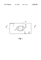
- FIG. 1 is a top view of a single orifice of a fully integrated thermal (FIT) fluid printhead architecture.
- FIT fully integrated thermal
- FIG. 2A is an isometric cross sectional view of a single orifice of a FIT fluid printhead showing the preferred embodiment of the integrated heat-sink.
- FIGS. 3A, 3B, and 3C cross sectional views show the process steps used to create the preferred embodiment.
- FIG. 4 is an isometric cross sectional view of a single orifice of a FIT fluid printhead showing a first-alternate embodiment of the integrated heat-sink.
- FIGS. 5A, 5B, and 5C cross sectional views show the process steps used to create the first-alternative embodiment.
- FIG. 6 is an isometric cross sectional view of a single orifice of a FIT fluid printhead showing a second-alternate embodiment of the integrated heat-sink.
- FIGS. 7A, 7B, and 7C cross sectional views show the process steps used to create the second-alternative embodiment.
- FIG. 8 is an isometric cross sectional view of a single orifice of a FIT fluid printhead showing a third-alternate embodiment of the integrated heat-sink.
- FIGS. 9A through 9E cross sectional views show the process steps to create the third-alternative embodiment.
- FIG. 9F shows the preferred pattern for creating the integrated heat-sink from FIGS. 9A-9F.
- FIG. 9G shows an alternate pattern if the fluid feed slots are oriented differently with respect to the fluid feed channel.
- FIG. 10 is an isometric cross sectional view of a single orifice of a FIT fluid printhead showing a fourth-alternate embodiment of the integrated heat-sink.
- FIGS. 11A through 11F cross sectional views show the process steps to create the fourth-embodiment.
- FIG. 12A shows an isometric view of the preferred embodiment of an exemplary printhead having multiple orifices.
- FIG. 12B shows an isometric view of the preferred embodiment of an exemplary printhead and its fluid feed channels and fluid feed slot openings.
- FIG. 13 shows an exemplary print cartridge using an exemplary printhead.
- FIG. 14 shows an exemplary recording device which uses the exemplary print cartridge.
- the fully integrated thermal (FIT) fluid-jet architecture as shown in FIG. 1 and FIG. 2 has an inherent thermal limitation. This limitation arises from the removal of semiconductor material to form a fluid feed channel 44 beneath the energy dissipation element 32 (typically a resistor integrated in a stack of thin-film layers 50). Previous architectures for printheads had semiconductor material beneath the resistors, thereby enabling heat to be effectively coupled to the surrounding bulk semiconductor substrate 20.
- a fluid such as ink
- the FIT architecture has a less effective heat path than before. Simulation and empirical testing have shown that the addition of a heat-sink attached to the stack of thin-film layers 50 and the semiconductor material adjacent to the fluid feed channels 44 allows residual heat to escape between firings of fluid from the orifices 42.
- the invention as seen in FIG. 2 essentially comprises forming a integrated heat-sink (shown here as metal layer 45 with adhesion layer 43), or a plurality of integrated heat-sinks, to a stack of thin-film layers exposed in the fluid feed channels 44 of a FIT printhead.
- the FIT printhead is comprised of a semiconductor substrate 20 with a stack of thin-film layers 50, including an energy dissipating element 32 and a plurality of fluid feed slots 30 defamed within the stack of thin-film layers 50, and an orifice layer 34.
- the orifice layer 34 has etched in it an orifice 42, or a pattern of orifices, positioned respective to the energy dissipation element 32 and exposing the fluid feed slots 30.
- the semiconductor substrate 20 has a fluid feed channel 44 etched in the side opposite to orifice 42.
- the fluid feed channel 44 is etched to expose the fluid feed slots 30.
- fluid is coupled from the fluid feed channel 44 through the fluid feed slots 30 directly into the cavity of orifice 32.
- the energy dissipation element 32 is energized and it heats the fluid to create a bubble which causes the remaining fluid in the orifice 42 to eject.
- the integrated heat-sink then removes any remaining heat from energy dissipating element 32 into semiconductor substrate 20 and fluid in the fluid feed channels 44.
- FIG. 1 shows a top view of a single orifice 42 in an orifice layer 34.
- Energy dissipation element 32 is typically a resistor, however, those skilled in the art will appreciate that other energy coupling devices such as piezoelectric or electro-restrictive materials are possible and still fall within the spirit and scope of the invention.
- Section AA shows the direction that cross-sections of various embodiments of the invention are viewed in later figures.
- FIG. 2 is an isometric drawing of a single orifice showing the basic structure of the FIT architecture with the preferred embodiment of the integrated heat-sink.
- a fluid such as ink, flows in the fluid feed channel 44, which is etched into a semiconductor substrate 20.
- FIGS. 3A-3C illustrate the process used to make the preferred embodiment.
- Applied on semiconductor substrate 20 is a stack of thin-film layers 50, which contain the energy dissipation element 32.
- An orifice layer 34 is applied on the stack of thin-film layers 50 and a nozzle orifice 42 (an opening or a hole) is created to expose the energy dissipation element 32 and fluid feed slots 30.
- the fluid feed slots 30 extend through the stack of thin-film layers and open into the fluid feed channel 44.
- the preferred embodiment applies a flash of an adhesion layer 43 (FIG. 3B), preferably tantalum, to a thickness of 100 to 500 Angstroms.
- a layer of metal 45 with a thickness of approximately 1 to 2 microns is then applied over the adhesion layer 43 (FIG. 3C).
- the metal layer 45 is preferably comprised of an inert metal such as gold, palladium, tungsten, or titanium tungsten, but preferably gold.
- the adhesion layer 43 and metal layer 45 would be deposited using a conventional physical vapor deposition process (see Thin Film Processes II, J. L. Vossen & W. Kern, editors, Academic Press, New York, 1991, ch. 2-4).
- a third layer (not shown) can be applied over the metal layer to provide an adhesion layer for attachment of the printhead to a cartridge.
- the adhesion layer 43 and metal layer 45 can be selectively placed by using photoresist and patterning an opening in those areas in which the adhesion layer 43 and metal layer 45 are desired.
- the patterning should at least be such that the inside of the fluid feed channel 44 is coated to create an effective heat path from 25 the stack of thin-film layers 50 to the semiconductor substrate 20. See FIGS. 9F and 9G for examples of pattern layouts (shown as area 17 and alternate area 17').
- FIG. 4 shows the first alternative embodiment which provides an integrated heat-sink that is formed by preprocessing the FIT semiconductor substrate 20 rather than post processing it as in the preferred embodiment.
- the integrated heat-sink is a layer of crystalline semiconductor 21, approximately 1 to 2 microns thick.
- FIGS. 5A-5C illustrate the process used to make the first alternate embodiment.
- the layer of crystalline semiconductor 21 is formed by conventionally masking the semiconductor substrate 20 with mask 36 to create a masked area opening which is the doped with a p-type dopant such as boron to an approximate depth of 1 to 2 microns.
- the mask 36 is then removed.
- a stack of thin-film layers 50 (FIG. 5B), which contains energy dissipating element 32 and has fluid feed slots 30 defined within, is then applied to the semiconductor substrate 20.
- An orifice layer 34 is then applied to the stack of thin-film layers 50 and an orifice 42 is etched in the orifice layer 34 which is positioned above energy dissipating element 32 and exposes fluid feed slots 30.
- the fluid feed slots 30 extend through the stack of thin-film layers 50 into fluid feed channel 44, which is created (in FIG. 5C) by etching. It is important in this first alternate embodiment that the semiconductor area in the location of the fluid feed slots 30 be masked to prevent the boron doping.
- the boron doping passivates the semiconductor substrate that has been doped from being etched when the fluid feed channel 44 is created by a tetramethyl ammonium hydroxide (TMAH) etch process (see U. Schnakenberg, W. Benecke and P. Lange, TMAHW Etchants for Silicon Micromaching, Tech. Dig., 6 th Int. Conf. Solid State Sensors and Actuators (Tranducers '91), San Francisco, Calif. USA, Jun. 24-28, 1991 pp.815-818).
- TMAH tetramethyl ammonium hydroxide
- FIG. 6 shows a second alternate embodiment which modifies the TMAH process used to create the fluid feed channels 44.
- This embodiment creates a layer of crystalline semiconductor 23 similar to the first alternate embodiment's doped crystalline semiconductor 21 but with the flexibility to greatly increase the thickness of the layer of crystalline semiconductor 23 and the ability to pattern the layer of crystalline semiconductor 23 to create fins 49 which increase the surface area of the heat-sink.
- FIGS. 7A-7C illustrate the process used to make the second alternate embodiment.
- FIG. 7A shows the semiconductor substrate 20 after it has been processed as described earlier to include the stack of thin-film layers 50 and the orifice layer 34.
- the energy dissipation element 32 is within the stack of thin-film layers 50.
- the orifice 42 is etched into the orifice layer 34 and is positioned over energy dissipation element 32 and exposes the fluid feed slots 30.
- the fluid feed slots 30 are defined as openings in the stack of thin-film layers 50.
- FIG. 7B shows the semiconductor substrate 20 after it has been partially etched in a TMAH etch process.
- the TMAH etching is stopped after a predefined time to create the desired thickness of the layer of crystalline semiconductor.
- a mask 27 is placed on the partially etched surface of the semiconductor substrate 20 to prevent etching where the mask 27 is present.
- An anisotropic dry etch is then performed to finish etching the semiconductor substrate 20 without undercutting under mask 27 to expose the fluid feed slots 30 to the fluid feed channel 44.
- An exemplary dry etch is a reactive ion etch (see Dry Etching for VLSI, A. J. van Roosmalen, J. A. G. Baggerman, & S. J. H. Brader, Plenum Press, New York, 1991).
- the semiconductor under the mask 27 is not etched thus forming fins 49, which remain after mask 27 is removed as shown in FIG. 7C.
- FIG. 8 shows the third alternate embodiment which creates the integrated heat-sink by applying a thermally-conductive material 25 on the semiconductor substrate 20 before the stack of thin-film layers 50 is applied.
- FIGS. 9A-9E illustrate the process used to create the third alternate embodiment.
- FIG. 9A shows the semiconductor substrate 20 with a layer of silicon dioxide 22 which has been grown and etched to form an area 17 (see commonly assigned U.S. Pat. No. 4,978,420 for representive etch techniques).
- FIG. 9B shows the application of a layer of thermally-conductive material 25, such as titanium tungsten (TiW), aluminium, or preferably tantalum which is placed in the area from which the layer of silicon dioxide 22 has been etched.
- FIG. 9C shows the application of a layer of phosphosilicate glass (PSG) which is applied over the layer of thermally-conductive material 25 and the layer of silicon dioxide 22.
- PSG phosphosilicate glass
- 9D is typically a composition of dielectric layers such as silicon nitride and silicon carbide.
- Protective layer 28 is typically a passivation layer of tantalum to protect the thin-film stack 50.
- the thin-film stack 50 could be any composition of thin-film layers and still fall within the spirit and scope of the invention.
- FIG. 9D shows the result after the remaining components of stack of thin-film layers 50, which includes energy dissipating element 32, and orifice layer 34 are processed as described earlier. Fluid feed slots 30 are defined during processing of the stack of thin-film layers 50. The orifice layer 34 is etched to create orifice 42.
- FIG. 9E shows the result of the TMAH etch used to create the fluid feed channel 44 which exposes the layer of thermally-conductive material 25.
- the layer of thermally-conductive material 25 transfers heat from the stack of thin-film layers 50 to the semiconductor substrate 20.
- FIG. 9F shows the layout of area 17 with respect to fluid feed slots 30 and fluid feed channel 44. This area 17 allows heat from energy dissipation element 32 to be conducted to both the semiconductor substrate and to the fluid in fluid feed slot 44.
- FIG. 9G shows an alternate area 17' that is used if fluid feed slots 30 are oriented as shown in fluid feed channel 44.
- This fluid feed slot orientation approach can also be used with other embodiments described within this specification and still fall within the spirit and scope of the invention.
- FIG. 10 represents a fourth alternate embodiment, which creates more surface area for the heat-sink described in the preferred embodiment.
- Fins 27 are formed by preprocessing the semiconductor substrate 20 to etch areas as described earlier before applying the stack of thin-film layers 50 and orifice layer 34.
- the fins 27 are comprised of silicon dioxide and PSG. Since these materials have low thermal conductivity, the fins 27 and the semiconductor substrate 20 are coated by phyical vapor deposition with an adhesion layer 43 and metal layer 45.
- the adhesion layer is preferably tantalum.
- the metal layer is an inert metal such as gold, palladium, or platinum, preferably gold.
- FIG. 11A-FIG. 11F illustrate the process steps used to create the fourth alternate embodiment.
- FIG. 11A shows the starting semiconductor substrate 20.
- the semiconductor substrate 20 is then etched, either isotropically or anisotropically to form, respectively, cross sectional viewed semi-circular or rectangular structures 19.
- FIG. 11A shows the result of the preferable anisotropic etch.
- An exemplary anisotropically etch is to use a conventional reactive ion etch technique (see W. Lang, Silicon Microstructuring Technology, Materials Science & Engineering, R17, p. 1-55, 1996).
- An exemplary isotropically etch is to use a conventional high frequency nitric chemistry technique.
- FIG. 11B shows the result from growing a conformal layer of silicon dioxide 22 on the semiconductor substrate 20.
- FIG. 11C shows the result after a conformal layer of PSG 24 is applied on the layer of silicon dioxide 22 and after it has been planarized using a resist etch-back, a spin-on-glass or preferably a chemical mechanical planarization (CMP) process.
- CMP chemical mechanical planarization
- the remaining stack of thin-film layers 50, including energy dissipating element 32 is then processed onto the conformal layer of PSG 24 in the manner described above as shown in FIG. 11D.
- FIG. 11D also shows the result after applying the orifice layer 34 and etching an orifice 42 which is positioned above energy dissipating element 32 and which exposes fluid feed slots 30 which extend through the stack of thin-film layers 50.
- FIG. 11E shows the result of the TMAH etch of the fluid feed channel 44 in the semiconductor substrate 20 which exposes the fins 27 which are comprised of silicon dioxide and PSG.
- FIG. 11F shows the result after a flash of adhesion layer 43, preferably tantalum, is applied across the surface of semiconductor substrate 20 and fins 27.
- a layer of metal 45 from one of the inert metals gold, palladium, or platinum, preferably gold. The metal layer 45 not only conducts heat to semiconductor substrate 20 but the increased surface area created by fins 27 help to transfer heat from the stack of thin-film layers 50 to the fluid in the fluid feed channel 44.
- FIG. 12A shows an exemplary printhead of the preferred embodiment constructed from semiconductor substrate 20, stack of thin-film layers 50 and orifice layer 34. A plurality of orifices 42 are etched in the orifice layer 34.
- the semiconductor substrate 20 also has an adhesion layer 43 and metal layer 45, which form the integrated heat-sink.
- FIG. 12B shows the reverse side of printhead 60. Fluid feed channels 44 direct fluid to fluid feed slots 30.
- FIG. 13 illustrates an exemplary print cartridge 100 that utilizes printhead 60.
- a print cartridge could be similar to a HP51626A available from Hewlett-Packard Co., but utilizing the inventive printhead described above.
- Printhead 60 is attached to a flex circuit 106 which electrically couples printhead 60 with electrical contacts 102. Orifices 42 eject liquid when appropriate control signals are applied to contacts 102.
- the fluid ejected is stored in fluid container 104.
- a fluid delivery assemblage an exemplary example being a sponge 108 and a standpipe (not shown), conveys the fluid in container 104 to the printhead 60 such that an adequate back pressure is maintained to prevent fluid leakage.
- FIG. 14 shows an exemplary recording apparatus 200, similar to a Hewlett-Packard Deskjet 340 (C2655A), for placing the fluid in cartridge 100, upon ejection from printhead 60, onto a medium 230.
- a conveyance assemblage 240 moves the cartridge 100 across the width of the media 230.
- Media feed mechanism 260 advances the media 230 past the printhead 60 to record along the length of the media 230. Additional media is supplied from media tray 210 after the recorded media 230 is ejected onto tray 220.
Abstract
Description
Claims (44)
Priority Applications (7)
| Application Number | Priority Date | Filing Date | Title |
|---|---|---|---|
| US09/033,504 US6126276A (en) | 1998-03-02 | 1998-03-02 | Fluid jet printhead with integrated heat-sink |
| US09/384,817 US6336714B1 (en) | 1996-02-07 | 1999-08-27 | Fully integrated thermal inkjet printhead having thin film layer shelf |
| US09/384,814 US6543884B1 (en) | 1996-02-07 | 1999-08-27 | Fully integrated thermal inkjet printhead having etched back PSG layer |
| US09/384,849 US6305790B1 (en) | 1996-02-07 | 1999-08-27 | Fully integrated thermal inkjet printhead having multiple ink feed holes per nozzle |
| US10/000,110 US6554404B2 (en) | 1996-02-07 | 2001-10-31 | Conductor routing for a printhead |
| US10/356,287 US6918657B2 (en) | 1996-02-07 | 2003-01-30 | Fully integrated thermal inkjet printhead having etched back PSG layer |
| US10/376,135 US6782621B2 (en) | 1996-02-07 | 2003-02-27 | Method of fabricating a fluid ejector |
Applications Claiming Priority (1)
| Application Number | Priority Date | Filing Date | Title |
|---|---|---|---|
| US09/033,504 US6126276A (en) | 1998-03-02 | 1998-03-02 | Fluid jet printhead with integrated heat-sink |
Related Parent Applications (2)
| Application Number | Title | Priority Date | Filing Date |
|---|---|---|---|
| US09/033,987 Continuation-In-Part US6162589A (en) | 1996-02-07 | 1998-03-02 | Direct imaging polymer fluid jet orifice |
| US09/314,551 Continuation-In-Part US6402972B1 (en) | 1996-02-07 | 1999-05-19 | Solid state ink jet print head and method of manufacture |
Related Child Applications (3)
| Application Number | Title | Priority Date | Filing Date |
|---|---|---|---|
| US09/314,551 Continuation-In-Part US6402972B1 (en) | 1996-02-07 | 1999-05-19 | Solid state ink jet print head and method of manufacture |
| US09/384,814 Continuation-In-Part US6543884B1 (en) | 1996-02-07 | 1999-08-27 | Fully integrated thermal inkjet printhead having etched back PSG layer |
| US09/384,817 Continuation-In-Part US6336714B1 (en) | 1996-02-07 | 1999-08-27 | Fully integrated thermal inkjet printhead having thin film layer shelf |
Publications (1)
| Publication Number | Publication Date |
|---|---|
| US6126276A true US6126276A (en) | 2000-10-03 |
Family
ID=21870779
Family Applications (1)
| Application Number | Title | Priority Date | Filing Date |
|---|---|---|---|
| US09/033,504 Expired - Lifetime US6126276A (en) | 1996-02-07 | 1998-03-02 | Fluid jet printhead with integrated heat-sink |
Country Status (1)
| Country | Link |
|---|---|
| US (1) | US6126276A (en) |
Cited By (29)
| Publication number | Priority date | Publication date | Assignee | Title |
|---|---|---|---|---|
| EP1205303A1 (en) * | 2000-11-07 | 2002-05-15 | Sony Corporation | Printer, printer head, and method of producing the printer head |
| US6425439B1 (en) * | 1999-11-09 | 2002-07-30 | Samsung Electronics Co., Ltd. | Cooling device with micro cooling fin |
| US20030210302A1 (en) * | 1997-08-28 | 2003-11-13 | Keefe Brian J. | Ink-jet printhead and method for producing the same |
| US20040005182A1 (en) * | 2002-07-03 | 2004-01-08 | Therics, Inc. | Apparatus, systems and methods for use in three-dimensional printing |
| US20040070649A1 (en) * | 2001-10-16 | 2004-04-15 | Hess Ulrich E. | Fluid-ejection devices and a deposition method for layers thereof |
| US20050206687A1 (en) * | 2003-10-03 | 2005-09-22 | Pugliese Roberto A Jr | Thin film coating of a slotted substrate and techniques for forming slotted substrates with partially patterned layers |
| US20050285904A1 (en) * | 2004-06-02 | 2005-12-29 | Canon Kabushiki Kaisha | Liquid ejecting head and liquid ejecting apparatus usable therewith |
| WO2006138158A1 (en) * | 2005-06-16 | 2006-12-28 | Hewlett-Packard Development Company, L.P. | Print head having extended surface elements |
| US20080017963A1 (en) * | 2006-07-24 | 2008-01-24 | Hung-Yi Lin | Si-substrate and structure of opto-electronic package having the same |
| US20080246814A1 (en) * | 2002-11-23 | 2008-10-09 | Silverbrook Research Pty Ltd | Inkjet printhead with nozzle arrangements having coated heater elements |
| US20090081867A1 (en) * | 2007-09-21 | 2009-03-26 | Shinko Electric Industries Co., Ltd. | Method of manufacturing substrate |
| US7594507B2 (en) | 2001-01-16 | 2009-09-29 | Hewlett-Packard Development Company, L.P. | Thermal generation of droplets for aerosol |
| US20090267108A1 (en) * | 2006-07-24 | 2009-10-29 | Hung-Yi Lin | Light emitting diode chip package and method of making the same |
| US20090273005A1 (en) * | 2006-07-24 | 2009-11-05 | Hung-Yi Lin | Opto-electronic package structure having silicon-substrate and method of forming the same |
| US20090273004A1 (en) * | 2006-07-24 | 2009-11-05 | Hung-Yi Lin | Chip package structure and method of making the same |
| US20120282715A1 (en) * | 2010-01-14 | 2012-11-08 | Canon Kabushiki Kaisha | Structure manufacturing method and liquid discharge head substrate manufacturing method |
| US20120329181A1 (en) * | 2011-06-21 | 2012-12-27 | Canon Kabushiki Kaisha | Method for producing liquid-discharge-head substrate |
| US9254535B2 (en) | 2014-06-20 | 2016-02-09 | Velo3D, Inc. | Apparatuses, systems and methods for three-dimensional printing |
| US9662840B1 (en) | 2015-11-06 | 2017-05-30 | Velo3D, Inc. | Adept three-dimensional printing |
| US9919360B2 (en) | 2016-02-18 | 2018-03-20 | Velo3D, Inc. | Accurate three-dimensional printing |
| US9962767B2 (en) | 2015-12-10 | 2018-05-08 | Velo3D, Inc. | Apparatuses for three-dimensional printing |
| US20180126649A1 (en) | 2016-11-07 | 2018-05-10 | Velo3D, Inc. | Gas flow in three-dimensional printing |
| US10144176B1 (en) | 2018-01-15 | 2018-12-04 | Velo3D, Inc. | Three-dimensional printing systems and methods of their use |
| US10252336B2 (en) | 2016-06-29 | 2019-04-09 | Velo3D, Inc. | Three-dimensional printing and three-dimensional printers |
| US10272525B1 (en) | 2017-12-27 | 2019-04-30 | Velo3D, Inc. | Three-dimensional printing systems and methods of their use |
| US10315252B2 (en) | 2017-03-02 | 2019-06-11 | Velo3D, Inc. | Three-dimensional printing of three-dimensional objects |
| US10449696B2 (en) | 2017-03-28 | 2019-10-22 | Velo3D, Inc. | Material manipulation in three-dimensional printing |
| US10611092B2 (en) | 2017-01-05 | 2020-04-07 | Velo3D, Inc. | Optics in three-dimensional printing |
| US11691343B2 (en) | 2016-06-29 | 2023-07-04 | Velo3D, Inc. | Three-dimensional printing and three-dimensional printers |
Citations (8)
| Publication number | Priority date | Publication date | Assignee | Title |
|---|---|---|---|---|
| US5159353A (en) * | 1991-07-02 | 1992-10-27 | Hewlett-Packard Company | Thermal inkjet printhead structure and method for making the same |
| US5665249A (en) * | 1994-10-17 | 1997-09-09 | Xerox Corporation | Micro-electromechanical die module with planarized thick film layer |
| US5710070A (en) * | 1996-11-08 | 1998-01-20 | Chartered Semiconductor Manufacturing Pte Ltd. | Application of titanium nitride and tungsten nitride thin film resistor for thermal ink jet technology |
| US5774148A (en) * | 1995-10-19 | 1998-06-30 | Lexmark International, Inc. | Printhead with field oxide as thermal barrier in chip |
| US5783474A (en) * | 1995-02-17 | 1998-07-21 | International Rectifier Corporation | Reduced mask process for manufacture of MOS gated devices using dopant-enhanced-oxidation of semiconductor |
| US5841452A (en) * | 1991-01-30 | 1998-11-24 | Canon Information Systems Research Australia Pty Ltd | Method of fabricating bubblejet print devices using semiconductor fabrication techniques |
| US5850241A (en) * | 1995-04-12 | 1998-12-15 | Eastman Kodak Company | Monolithic print head structure and a manufacturing process therefor using anisotropic wet etching |
| US5900894A (en) * | 1996-04-08 | 1999-05-04 | Fuji Xerox Co., Ltd. | Ink jet print head, method for manufacturing the same, and ink jet recording device |
-
1998
- 1998-03-02 US US09/033,504 patent/US6126276A/en not_active Expired - Lifetime
Patent Citations (8)
| Publication number | Priority date | Publication date | Assignee | Title |
|---|---|---|---|---|
| US5841452A (en) * | 1991-01-30 | 1998-11-24 | Canon Information Systems Research Australia Pty Ltd | Method of fabricating bubblejet print devices using semiconductor fabrication techniques |
| US5159353A (en) * | 1991-07-02 | 1992-10-27 | Hewlett-Packard Company | Thermal inkjet printhead structure and method for making the same |
| US5665249A (en) * | 1994-10-17 | 1997-09-09 | Xerox Corporation | Micro-electromechanical die module with planarized thick film layer |
| US5783474A (en) * | 1995-02-17 | 1998-07-21 | International Rectifier Corporation | Reduced mask process for manufacture of MOS gated devices using dopant-enhanced-oxidation of semiconductor |
| US5850241A (en) * | 1995-04-12 | 1998-12-15 | Eastman Kodak Company | Monolithic print head structure and a manufacturing process therefor using anisotropic wet etching |
| US5774148A (en) * | 1995-10-19 | 1998-06-30 | Lexmark International, Inc. | Printhead with field oxide as thermal barrier in chip |
| US5900894A (en) * | 1996-04-08 | 1999-05-04 | Fuji Xerox Co., Ltd. | Ink jet print head, method for manufacturing the same, and ink jet recording device |
| US5710070A (en) * | 1996-11-08 | 1998-01-20 | Chartered Semiconductor Manufacturing Pte Ltd. | Application of titanium nitride and tungsten nitride thin film resistor for thermal ink jet technology |
Cited By (87)
| Publication number | Priority date | Publication date | Assignee | Title |
|---|---|---|---|---|
| US20030210302A1 (en) * | 1997-08-28 | 2003-11-13 | Keefe Brian J. | Ink-jet printhead and method for producing the same |
| US7048359B2 (en) * | 1997-08-28 | 2006-05-23 | Hewlett-Packard Development Company, L.P. | Ink-jet printhead and method for producing the same |
| US6425439B1 (en) * | 1999-11-09 | 2002-07-30 | Samsung Electronics Co., Ltd. | Cooling device with micro cooling fin |
| US6685304B2 (en) | 2000-11-07 | 2004-02-03 | Sony Corporation | Printer, printer head and method of producing the print head to promote reliable bonding of print head structures |
| EP1205303A1 (en) * | 2000-11-07 | 2002-05-15 | Sony Corporation | Printer, printer head, and method of producing the printer head |
| US7594507B2 (en) | 2001-01-16 | 2009-09-29 | Hewlett-Packard Development Company, L.P. | Thermal generation of droplets for aerosol |
| US7025894B2 (en) | 2001-10-16 | 2006-04-11 | Hewlett-Packard Development Company, L.P. | Fluid-ejection devices and a deposition method for layers thereof |
| US7517060B2 (en) | 2001-10-16 | 2009-04-14 | Hewlett-Packard Development Company, L.P. | Fluid-ejection devices and a deposition method for layers thereof |
| US20040070649A1 (en) * | 2001-10-16 | 2004-04-15 | Hess Ulrich E. | Fluid-ejection devices and a deposition method for layers thereof |
| US20060125882A1 (en) * | 2001-10-16 | 2006-06-15 | Hess Ulrich E | Fluid-ejection devices and a deposition method for layers thereof |
| US7027887B2 (en) | 2002-07-03 | 2006-04-11 | Theries, Llc | Apparatus, systems and methods for use in three-dimensional printing |
| US20040118309A1 (en) * | 2002-07-03 | 2004-06-24 | Therics, Inc. | Apparatus, systems and methods for use in three-dimensional printing |
| US6986654B2 (en) | 2002-07-03 | 2006-01-17 | Therics, Inc. | Apparatus, systems and methods for use in three-dimensional printing |
| US20040005182A1 (en) * | 2002-07-03 | 2004-01-08 | Therics, Inc. | Apparatus, systems and methods for use in three-dimensional printing |
| US20040003738A1 (en) * | 2002-07-03 | 2004-01-08 | Therics, Inc. | Apparatus, systems and methods for use in three-dimensional printing |
| US6905645B2 (en) | 2002-07-03 | 2005-06-14 | Therics, Inc. | Apparatus, systems and methods for use in three-dimensional printing |
| WO2004005014A3 (en) * | 2002-07-03 | 2004-07-08 | Therics Inc | Three-dimensional printing method and apparatus |
| US7073442B2 (en) | 2002-07-03 | 2006-07-11 | Afbs, Inc. | Apparatus, systems and methods for use in three-dimensional printing |
| US20080246814A1 (en) * | 2002-11-23 | 2008-10-09 | Silverbrook Research Pty Ltd | Inkjet printhead with nozzle arrangements having coated heater elements |
| US20050206687A1 (en) * | 2003-10-03 | 2005-09-22 | Pugliese Roberto A Jr | Thin film coating of a slotted substrate and techniques for forming slotted substrates with partially patterned layers |
| US7594328B2 (en) * | 2003-10-03 | 2009-09-29 | Hewlett-Packard Development Company, L.P. | Method of forming a slotted substrate with partially patterned layers |
| US20050285904A1 (en) * | 2004-06-02 | 2005-12-29 | Canon Kabushiki Kaisha | Liquid ejecting head and liquid ejecting apparatus usable therewith |
| US8109610B2 (en) | 2004-06-02 | 2012-02-07 | Canon Kabushiki Kaisha | Liquid ejecting head and liquid ejecting apparatus usable therewith |
| US20090295874A1 (en) * | 2004-06-02 | 2009-12-03 | Canon Kabushiki Kaisha | Liquid ejecting head and liquid ejecting apparatus usable therewith |
| US7591538B2 (en) | 2004-06-02 | 2009-09-22 | Canon Kabushiki Kaisha | Liquid ejecting head and liquid ejecting apparatus usable therewith |
| WO2006138158A1 (en) * | 2005-06-16 | 2006-12-28 | Hewlett-Packard Development Company, L.P. | Print head having extended surface elements |
| KR101280194B1 (en) * | 2005-06-16 | 2013-06-28 | 휴렛-팩커드 디벨롭먼트 컴퍼니, 엘.피. | Print head having extended surface elements |
| CN101198473B (en) * | 2005-06-16 | 2012-05-30 | 惠普开发有限公司 | Print head and its forming method and cooling method |
| US20090051741A1 (en) * | 2005-06-16 | 2009-02-26 | Blair Dustin W | Print head having extended surface elements |
| US7959264B2 (en) | 2005-06-16 | 2011-06-14 | Hewlett-Packard Development Company, L.P. | Print head having extended surface elements |
| US20080017876A1 (en) * | 2006-07-24 | 2008-01-24 | Hung-Yi Lin | Si-substrate and structure of opto-electronic package having the same |
| US20090273005A1 (en) * | 2006-07-24 | 2009-11-05 | Hung-Yi Lin | Opto-electronic package structure having silicon-substrate and method of forming the same |
| US20090273004A1 (en) * | 2006-07-24 | 2009-11-05 | Hung-Yi Lin | Chip package structure and method of making the same |
| US20090267108A1 (en) * | 2006-07-24 | 2009-10-29 | Hung-Yi Lin | Light emitting diode chip package and method of making the same |
| US7732233B2 (en) | 2006-07-24 | 2010-06-08 | Touch Micro-System Technology Corp. | Method for making light emitting diode chip package |
| US20080017880A1 (en) * | 2006-07-24 | 2008-01-24 | Hung-Yi Lin | Si-substrate and structure of opto-electronic package having the same |
| US20080017962A1 (en) * | 2006-07-24 | 2008-01-24 | Hung-Yi Lin | Si-substrate and structure of opto-electronic package having the same |
| US20080017963A1 (en) * | 2006-07-24 | 2008-01-24 | Hung-Yi Lin | Si-substrate and structure of opto-electronic package having the same |
| US20090081867A1 (en) * | 2007-09-21 | 2009-03-26 | Shinko Electric Industries Co., Ltd. | Method of manufacturing substrate |
| US7981798B2 (en) * | 2007-09-21 | 2011-07-19 | Shinko Electric Industries Co., Ltd. | Method of manufacturing substrate |
| US8518725B2 (en) * | 2010-01-14 | 2013-08-27 | Canon Kabushiki Kaisha | Structure manufacturing method and liquid discharge head substrate manufacturing method |
| US20120282715A1 (en) * | 2010-01-14 | 2012-11-08 | Canon Kabushiki Kaisha | Structure manufacturing method and liquid discharge head substrate manufacturing method |
| KR101364918B1 (en) * | 2010-01-14 | 2014-02-19 | 캐논 가부시끼가이샤 | Structure manufacturing method and liquid discharge head substrate manufacturing method |
| US20120329181A1 (en) * | 2011-06-21 | 2012-12-27 | Canon Kabushiki Kaisha | Method for producing liquid-discharge-head substrate |
| US8951815B2 (en) * | 2011-06-21 | 2015-02-10 | Canon Kabushiki Kaisha | Method for producing liquid-discharge-head substrate |
| US9486878B2 (en) | 2014-06-20 | 2016-11-08 | Velo3D, Inc. | Apparatuses, systems and methods for three-dimensional printing |
| US9346127B2 (en) | 2014-06-20 | 2016-05-24 | Velo3D, Inc. | Apparatuses, systems and methods for three-dimensional printing |
| US9399256B2 (en) | 2014-06-20 | 2016-07-26 | Velo3D, Inc. | Apparatuses, systems and methods for three-dimensional printing |
| US9403235B2 (en) | 2014-06-20 | 2016-08-02 | Velo3D, Inc. | Apparatuses, systems and methods for three-dimensional printing |
| US10195693B2 (en) | 2014-06-20 | 2019-02-05 | Vel03D, Inc. | Apparatuses, systems and methods for three-dimensional printing |
| US9573193B2 (en) | 2014-06-20 | 2017-02-21 | Velo3D, Inc. | Apparatuses, systems and methods for three-dimensional printing |
| US9573225B2 (en) | 2014-06-20 | 2017-02-21 | Velo3D, Inc. | Apparatuses, systems and methods for three-dimensional printing |
| US9586290B2 (en) | 2014-06-20 | 2017-03-07 | Velo3D, Inc. | Systems for three-dimensional printing |
| US10507549B2 (en) | 2014-06-20 | 2019-12-17 | Velo3D, Inc. | Apparatuses, systems and methods for three-dimensional printing |
| US10493564B2 (en) | 2014-06-20 | 2019-12-03 | Velo3D, Inc. | Apparatuses, systems and methods for three-dimensional printing |
| US9821411B2 (en) | 2014-06-20 | 2017-11-21 | Velo3D, Inc. | Apparatuses, systems and methods for three-dimensional printing |
| US9254535B2 (en) | 2014-06-20 | 2016-02-09 | Velo3D, Inc. | Apparatuses, systems and methods for three-dimensional printing |
| US10357957B2 (en) | 2015-11-06 | 2019-07-23 | Velo3D, Inc. | Adept three-dimensional printing |
| US10065270B2 (en) | 2015-11-06 | 2018-09-04 | Velo3D, Inc. | Three-dimensional printing in real time |
| US9662840B1 (en) | 2015-11-06 | 2017-05-30 | Velo3D, Inc. | Adept three-dimensional printing |
| US9676145B2 (en) | 2015-11-06 | 2017-06-13 | Velo3D, Inc. | Adept three-dimensional printing |
| US10286603B2 (en) | 2015-12-10 | 2019-05-14 | Velo3D, Inc. | Skillful three-dimensional printing |
| US10688722B2 (en) | 2015-12-10 | 2020-06-23 | Velo3D, Inc. | Skillful three-dimensional printing |
| US10058920B2 (en) | 2015-12-10 | 2018-08-28 | Velo3D, Inc. | Skillful three-dimensional printing |
| US10071422B2 (en) | 2015-12-10 | 2018-09-11 | Velo3D, Inc. | Skillful three-dimensional printing |
| US10183330B2 (en) | 2015-12-10 | 2019-01-22 | Vel03D, Inc. | Skillful three-dimensional printing |
| US9962767B2 (en) | 2015-12-10 | 2018-05-08 | Velo3D, Inc. | Apparatuses for three-dimensional printing |
| US10207454B2 (en) | 2015-12-10 | 2019-02-19 | Velo3D, Inc. | Systems for three-dimensional printing |
| US9931697B2 (en) | 2016-02-18 | 2018-04-03 | Velo3D, Inc. | Accurate three-dimensional printing |
| US10252335B2 (en) | 2016-02-18 | 2019-04-09 | Vel03D, Inc. | Accurate three-dimensional printing |
| US9919360B2 (en) | 2016-02-18 | 2018-03-20 | Velo3D, Inc. | Accurate three-dimensional printing |
| US10434573B2 (en) | 2016-02-18 | 2019-10-08 | Velo3D, Inc. | Accurate three-dimensional printing |
| US10252336B2 (en) | 2016-06-29 | 2019-04-09 | Velo3D, Inc. | Three-dimensional printing and three-dimensional printers |
| US11691343B2 (en) | 2016-06-29 | 2023-07-04 | Velo3D, Inc. | Three-dimensional printing and three-dimensional printers |
| US10286452B2 (en) | 2016-06-29 | 2019-05-14 | Velo3D, Inc. | Three-dimensional printing and three-dimensional printers |
| US10259044B2 (en) | 2016-06-29 | 2019-04-16 | Velo3D, Inc. | Three-dimensional printing and three-dimensional printers |
| US20180126649A1 (en) | 2016-11-07 | 2018-05-10 | Velo3D, Inc. | Gas flow in three-dimensional printing |
| US10661341B2 (en) | 2016-11-07 | 2020-05-26 | Velo3D, Inc. | Gas flow in three-dimensional printing |
| US10611092B2 (en) | 2017-01-05 | 2020-04-07 | Velo3D, Inc. | Optics in three-dimensional printing |
| US10315252B2 (en) | 2017-03-02 | 2019-06-11 | Velo3D, Inc. | Three-dimensional printing of three-dimensional objects |
| US10442003B2 (en) | 2017-03-02 | 2019-10-15 | Velo3D, Inc. | Three-dimensional printing of three-dimensional objects |
| US10369629B2 (en) | 2017-03-02 | 2019-08-06 | Veo3D, Inc. | Three-dimensional printing of three-dimensional objects |
| US10357829B2 (en) | 2017-03-02 | 2019-07-23 | Velo3D, Inc. | Three-dimensional printing of three-dimensional objects |
| US10888925B2 (en) | 2017-03-02 | 2021-01-12 | Velo3D, Inc. | Three-dimensional printing of three-dimensional objects |
| US10449696B2 (en) | 2017-03-28 | 2019-10-22 | Velo3D, Inc. | Material manipulation in three-dimensional printing |
| US10272525B1 (en) | 2017-12-27 | 2019-04-30 | Velo3D, Inc. | Three-dimensional printing systems and methods of their use |
| US10144176B1 (en) | 2018-01-15 | 2018-12-04 | Velo3D, Inc. | Three-dimensional printing systems and methods of their use |
Similar Documents
| Publication | Publication Date | Title |
|---|---|---|
| US6126276A (en) | Fluid jet printhead with integrated heat-sink | |
| JP2994344B2 (en) | Ink jet print head and method of forming the same | |
| US6365058B1 (en) | Method of manufacturing a fluid ejection device with a fluid channel therethrough | |
| JP4571734B2 (en) | Fluid drop generator and method of manufacturing the same | |
| US5635966A (en) | Edge feed ink delivery thermal inkjet printhead structure and method of fabrication | |
| TWI265094B (en) | Slotted substrate and method of making | |
| JP2001071504A (en) | Printer having ink jet print head, manufacture thereof and method for printing | |
| US6065823A (en) | Heat spreader for ink-jet printhead | |
| US6785956B2 (en) | Method of fabricating a fluid jet printhead | |
| TW521040B (en) | Fully integrated thermal inkjet printhead having thin film layer shelf | |
| US6718632B2 (en) | Method of making a fluid-jet ejection device | |
| EP0438295B1 (en) | Thermal ink jet printheads | |
| KR100717023B1 (en) | Inkjet printhead and method of manufacturing the same | |
| JP2002192723A (en) | Printer, method for forming the same, and printing method | |
| US4835553A (en) | Thermal ink jet printhead with increased drop generation rate | |
| JP2005022402A (en) | Ink-jet printhead | |
| KR100717022B1 (en) | Inkjet printhead and method of manufacturing the same | |
| US6558969B2 (en) | Fluid-jet printhead and method of fabricating a fluid-jet printhead | |
| US6776915B2 (en) | Method of manufacturing a fluid ejection device with a fluid channel therethrough | |
| JPH0441242A (en) | Ink jet recorder | |
| JP4562248B2 (en) | Inkjet head | |
| JPH06126961A (en) | Ink jet recording head | |
| JP2002011882A (en) | Ink jet recording head | |
| JP2002326358A (en) | Ink jet head |
Legal Events
| Date | Code | Title | Description |
|---|---|---|---|
| AS | Assignment |
Owner name: HEWLETT-PACKARD COMPANY, CALIFORNIA Free format text: ASSIGNMENT OF ASSIGNORS INTEREST;ASSIGNORS:DAVIS, COLIN C.;KAWAMURA, NAOTO;BEERLING, TIMOTHY;AND OTHERS;REEL/FRAME:009296/0694;SIGNING DATES FROM 19980302 TO 19980407 |
|
| STCF | Information on status: patent grant |
Free format text: PATENTED CASE |
|
| AS | Assignment |
Owner name: HEWLETT-PACKARD COMPANY, COLORADO Free format text: MERGER;ASSIGNOR:HEWLETT-PACKARD COMPANY;REEL/FRAME:011523/0469 Effective date: 19980520 |
|
| FEPP | Fee payment procedure |
Free format text: PAYOR NUMBER ASSIGNED (ORIGINAL EVENT CODE: ASPN); ENTITY STATUS OF PATENT OWNER: LARGE ENTITY |
|
| FPAY | Fee payment |
Year of fee payment: 4 |
|
| FPAY | Fee payment |
Year of fee payment: 8 |
|
| AS | Assignment |
Owner name: HEWLETT-PACKARD DEVELOPMENT COMPANY, L.P., TEXAS Free format text: ASSIGNMENT OF ASSIGNORS INTEREST;ASSIGNOR:HEWLETT-PACKARD COMPANY;REEL/FRAME:026945/0699 Effective date: 20030131 |
|
| FPAY | Fee payment |
Year of fee payment: 12 |