US6097464A - Multi-domain homeotropic aligned liquid crystal display having cruciform bumps formed around pixel electrodes - Google Patents
Multi-domain homeotropic aligned liquid crystal display having cruciform bumps formed around pixel electrodes Download PDFInfo
- Publication number
- US6097464A US6097464A US09/484,395 US48439500A US6097464A US 6097464 A US6097464 A US 6097464A US 48439500 A US48439500 A US 48439500A US 6097464 A US6097464 A US 6097464A
- Authority
- US
- United States
- Prior art keywords
- liquid crystal
- crystal display
- aligned liquid
- homeotropic aligned
- domain
- Prior art date
- Legal status (The legal status is an assumption and is not a legal conclusion. Google has not performed a legal analysis and makes no representation as to the accuracy of the status listed.)
- Expired - Lifetime
Links
Images


Classifications
-
- G—PHYSICS
- G02—OPTICS
- G02F—OPTICAL DEVICES OR ARRANGEMENTS FOR THE CONTROL OF LIGHT BY MODIFICATION OF THE OPTICAL PROPERTIES OF THE MEDIA OF THE ELEMENTS INVOLVED THEREIN; NON-LINEAR OPTICS; FREQUENCY-CHANGING OF LIGHT; OPTICAL LOGIC ELEMENTS; OPTICAL ANALOGUE/DIGITAL CONVERTERS
- G02F1/00—Devices or arrangements for the control of the intensity, colour, phase, polarisation or direction of light arriving from an independent light source, e.g. switching, gating or modulating; Non-linear optics
- G02F1/01—Devices or arrangements for the control of the intensity, colour, phase, polarisation or direction of light arriving from an independent light source, e.g. switching, gating or modulating; Non-linear optics for the control of the intensity, phase, polarisation or colour
- G02F1/13—Devices or arrangements for the control of the intensity, colour, phase, polarisation or direction of light arriving from an independent light source, e.g. switching, gating or modulating; Non-linear optics for the control of the intensity, phase, polarisation or colour based on liquid crystals, e.g. single liquid crystal display cells
- G02F1/133—Constructional arrangements; Operation of liquid crystal cells; Circuit arrangements
- G02F1/1333—Constructional arrangements; Manufacturing methods
- G02F1/1337—Surface-induced orientation of the liquid crystal molecules, e.g. by alignment layers
- G02F1/133753—Surface-induced orientation of the liquid crystal molecules, e.g. by alignment layers with different alignment orientations or pretilt angles on a same surface, e.g. for grey scale or improved viewing angle
-
- G—PHYSICS
- G02—OPTICS
- G02F—OPTICAL DEVICES OR ARRANGEMENTS FOR THE CONTROL OF LIGHT BY MODIFICATION OF THE OPTICAL PROPERTIES OF THE MEDIA OF THE ELEMENTS INVOLVED THEREIN; NON-LINEAR OPTICS; FREQUENCY-CHANGING OF LIGHT; OPTICAL LOGIC ELEMENTS; OPTICAL ANALOGUE/DIGITAL CONVERTERS
- G02F1/00—Devices or arrangements for the control of the intensity, colour, phase, polarisation or direction of light arriving from an independent light source, e.g. switching, gating or modulating; Non-linear optics
- G02F1/01—Devices or arrangements for the control of the intensity, colour, phase, polarisation or direction of light arriving from an independent light source, e.g. switching, gating or modulating; Non-linear optics for the control of the intensity, phase, polarisation or colour
- G02F1/13—Devices or arrangements for the control of the intensity, colour, phase, polarisation or direction of light arriving from an independent light source, e.g. switching, gating or modulating; Non-linear optics for the control of the intensity, phase, polarisation or colour based on liquid crystals, e.g. single liquid crystal display cells
- G02F1/137—Devices or arrangements for the control of the intensity, colour, phase, polarisation or direction of light arriving from an independent light source, e.g. switching, gating or modulating; Non-linear optics for the control of the intensity, phase, polarisation or colour based on liquid crystals, e.g. single liquid crystal display cells characterised by the electro-optical or magneto-optical effect, e.g. field-induced phase transition, orientation effect, guest-host interaction or dynamic scattering
- G02F1/139—Devices or arrangements for the control of the intensity, colour, phase, polarisation or direction of light arriving from an independent light source, e.g. switching, gating or modulating; Non-linear optics for the control of the intensity, phase, polarisation or colour based on liquid crystals, e.g. single liquid crystal display cells characterised by the electro-optical or magneto-optical effect, e.g. field-induced phase transition, orientation effect, guest-host interaction or dynamic scattering based on orientation effects in which the liquid crystal remains transparent
- G02F1/1393—Devices or arrangements for the control of the intensity, colour, phase, polarisation or direction of light arriving from an independent light source, e.g. switching, gating or modulating; Non-linear optics for the control of the intensity, phase, polarisation or colour based on liquid crystals, e.g. single liquid crystal display cells characterised by the electro-optical or magneto-optical effect, e.g. field-induced phase transition, orientation effect, guest-host interaction or dynamic scattering based on orientation effects in which the liquid crystal remains transparent the birefringence of the liquid crystal being electrically controlled, e.g. ECB-, DAP-, HAN-, PI-LC cells
-
- G—PHYSICS
- G02—OPTICS
- G02F—OPTICAL DEVICES OR ARRANGEMENTS FOR THE CONTROL OF LIGHT BY MODIFICATION OF THE OPTICAL PROPERTIES OF THE MEDIA OF THE ELEMENTS INVOLVED THEREIN; NON-LINEAR OPTICS; FREQUENCY-CHANGING OF LIGHT; OPTICAL LOGIC ELEMENTS; OPTICAL ANALOGUE/DIGITAL CONVERTERS
- G02F1/00—Devices or arrangements for the control of the intensity, colour, phase, polarisation or direction of light arriving from an independent light source, e.g. switching, gating or modulating; Non-linear optics
- G02F1/01—Devices or arrangements for the control of the intensity, colour, phase, polarisation or direction of light arriving from an independent light source, e.g. switching, gating or modulating; Non-linear optics for the control of the intensity, phase, polarisation or colour
- G02F1/13—Devices or arrangements for the control of the intensity, colour, phase, polarisation or direction of light arriving from an independent light source, e.g. switching, gating or modulating; Non-linear optics for the control of the intensity, phase, polarisation or colour based on liquid crystals, e.g. single liquid crystal display cells
- G02F1/133—Constructional arrangements; Operation of liquid crystal cells; Circuit arrangements
- G02F1/1333—Constructional arrangements; Manufacturing methods
- G02F1/1337—Surface-induced orientation of the liquid crystal molecules, e.g. by alignment layers
- G02F1/133707—Structures for producing distorted electric fields, e.g. bumps, protrusions, recesses, slits in pixel electrodes
Definitions
- the present invention relates generally to a structure of a multi-domain liquid crystal display (MD-LCD) and its manufacturing method, and more specifically to a structure of a multi-domain homeotropic aligned liquid crystal display (MHA-LCD) with cruciform bumps forming around pixel electrodes and the method for manufacturing the structure.
- MD-LCD multi-domain liquid crystal display
- MHA-LCD multi-domain homeotropic aligned liquid crystal display
- Controlling liquid crystal domains is the most important technology in obtaining a wide-viewing angle for a vertically aligned LCD.
- Most of the conventional LCD's are 90° twisted nematic (TN) LCD's having a LCD panel and crossed polarizers attached outside.
- the drawbacks of the conventional LCD's include narrow viewing angles ( ⁇ 40° horizontally and ⁇ 30° vertically), slow response (about 50 ms), and large color dispersion. Therefore, it is difficult to make high quality LCD panels. Also, the rubbing process required in manufacturing the panels causes electric static damage (ESD) and particle pollution.
- ESD electric static damage
- LCD panels Because of the demand in high quality LCD panels with a wide-viewing angle, the structure of multi-domain vertically aligned LCDs has been developed. Such LCD panels have compensation films and crossed polarizers outside the liquid crystal display panel. The liquid crystal mode is multi-domain vertically aligned. The LCD panel has a wide-viewing angle and small color dispersion. In addition, it does not have electric static damage and particle pollution problems because no rubbing process is required.
- the ridge and fringe field homeotropic aligned (RFFHA) structure of IBM has a Y and inversed-Y shaped bump structure as shown in FIG. 1.
- the Y and inversed-Y shaped bump structure is formed in the central portion of a pixel electrode.
- Fujitsu's multi-domain vertically aligned (MVA) structure has W-shaped bump structures as shown FIG. 2.
- the W-shaped bump structures are formed on both upper and lower substrates.
- the present invention has been made to overcome the drawbacks of the conventional structure of a multi-domain vertically aligned LCD mentioned above.
- the primary object of the present invention is to provide a structure of a multi-domain homeotropic aligned liquid crystal display with cruciform bumps forming around pixel electrodes.
- the structure of the cruciform bump in present invention is constructed on a substrate that has a color filter or a thin film transistor (TFT).
- the cruciform bumps of the present invention are formed around the pixel electrodes. Because of the bump structure, the liquid crystal molecules are pre-tilted with high tilt angles which result in orderly alignment of liquid crystal molecules after an external electric field is applied. Consequently, four domains are formed.
- the cruciform bump in the present invention provides the advantages of optical response faster than 30 ms, an all viewing angle larger than 140°, a high contrast ratio (CR) more than 700, response faster than 16.5 ms on some gray levels and small color dispersion. Moreover, the horizontal and vertical viewing angles can be as large as 50° when the CR is more than 200.
- Another object of the present invention is to provide the method of manufacturing the above-mentioned cruciform bump structure of the MHA-LCD.
- Standard photo-lithographic process or back side exposure (BSE) method is used to manufacture the cruciform bump structure of this invention.
- BSE back side exposure
- the advantages of this manufacturing method are fast, simple, clean and no pollution.
- the method requires only one substrate with bumps fabricated thereon to form multi-domain cells. Therefore, the light intensity of the liquid crystal mode can reach up to 55% of that of a 90° twisted nematic LCD, and is 20% higher than that of a conventional vertically aligned wide-viewing angle LCD.
- FIG. 1 is a diagram of the conventional multi-domain vertically aligned LCD illustrating the "double-Y" shaped bump structure of IBM's RFFHA-LCD.
- FIG. 2 is a diagram of another conventional multi-domain vertically aligned LCD illustrating the W shaped bump structure of Fujitsu's MVA-LCD.
- FIG. 3 is a cross-sectional view of a multi-domain homeotropic aligned liquid crystal display according to the invention.
- FIG. 4a is a top view of a cruciform bump formed around a pixel electrode in a multi-domain homeotropic aligned liquid crystal display according to the invention.
- FIG. 4b is a diagram illustrating various dimensions of a cruciform bump formed around a pixel electrode in a multi-domain homeotropic aligned liquid crystal display according to the invention.
- FIG. 5 is a diagram illustrating the BSE process for fabricating the cruciform bump shown in FIG. 4.
- FIG. 6 shows the side view of the novel structure and the operation mechanism of a multi-domain homeotropic aligned liquid crystal display according to the invention.
- FIG. 7a shows the optical texture when the absorbing axis of crossed polarizers of a multi-domain homeotropic aligned liquid crystal display according to the invention are placed at ⁇ 45° directions respectively with a voltage being applied.
- FIG. 7b shows the optical texture when the absorbing axis of crossed polarizers of a multi-domain homeotropic aligned liquid crystal display according to the invention are placed at 0° and 90° directions respectively with a voltage being applied.
- FIGS. 8(a)-8(f) show the electrode patterns on the pixel electrode or the common electrode of a multi-domain homeotropic aligned liquid crystal display according to the invention.
- FIG. 9 shows the voltage-dependent transmittance curve in the multi-domain homeotropic aligned liquid crystal display according to the invention.
- FIG. 10 shows the optical response in a multi-domain homeotropic aligned liquid crystal display according to the invention.
- FIG. 11 shows the response between the gray levels in a multi-domain homeotropic aligned liquid crystal display according to the invention.
- FIG. 12 shows the iso-contrast contours of a multi-domain homeotropic aligned liquid crystal display according to the invention with compensator A- and C-plates.
- FIG. 13 shows the color shift in a multi-domain homeotropic aligned liquid crystal display according to the invention.
- the operating principle of the multi-domain homeotropic aligned liquid crystal display mode in this invention is a combination effect of a fringe field and bump structure. Based on the effect, multi-domain units are formed to provide a wide-viewing angle. According to this invention, the tilt direction of liquid crystal molecules can be controlled when a voltage is applied.
- Cruciform bump structures are constructed on a color filter or TFT substrate. Compensation films and crossed polarizers are attached outside a liquid crystal display panel.
- FIG. 3 is a cross-sectional view of a multi-domain homeotropic aligned liquid crystal display according to the invention.
- the LCD structure 300 comprises a liquid crystal cell, a pair of crossed polarizers 301 and 302, compensation films 303 and 304, and a cruciform bump structure 310.
- the liquid crystal cell comprises a pixel electrode layer 305, a common electrode layer 306 and a pair of parallel substrates 308 and 309 filled with liquid crystals 307.
- the crossed polarizers 301 and 302 are attached outside the liquid crystal cell.
- the compensation films 303 and 304 are located between the crossed polarizers 301 and 302.
- the cruciform bump structure 310 is built around the pixel electrode.
- the compensation films can be combinations of negative birefrigence and uni-axial birefrigence, such as a C-plate and an A-plate or at least one bi-axial film.
- the pixel electrode may be a pixel unit driven by a switching device of an active matrix. Its structure can be co-plane with, above, or below the active matrix.
- the active matrix may be a thin film transistor made of amorphous silicon, single silicon, poly-silicon, or low temperature poly-silicon, or a plasma address device.
- the cruciform bumps formed around the pixel electrode are fabricated by a standard photo-lithographic process or a self-aligned BSE method.
- the steps of fabricating cruciform bumps by using a standard photo-lithographic process include substrate formation, coating, pre-bake, exposure, development, mid-bake and hard-bake.
- a substrate with controlling devices such as thin film transistors and electrode layers is first prepared.
- the top surface of the substrate is coated with a photoresist layer.
- the substrate coated with photoresist is placed on a hot plate for pre-bake.
- a photomask is then used to cover and pattern the substrate by exposing the substrate to light from its front side.
- the substrate is then developed to form the bump structure.
- the shape of the bump is further improved in a mid-bake step.
- the bump is harden.
- the cruciform bumps are formed around the pixel electrodes. Those bumps direct and pre-tilt liquid crystal molecules with high tilt angles which result in the alignment of liquid crystal molecules to form four-domain textures after a voltage is applied.
- the cruciform bumps can be fabricated either on the top or on the bottom of the electrode layer.
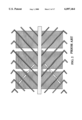
- FIG. 4a is a top view of the cruciform bumps formed around a pixel electrode in a multi-domain homeotropic aligned liquid crystal display of the present invention.
- a polymer bump structure 401 is built on the bus line of a thin film transistor substrate 402.
- the bump structure 401 around the pixel electrodes 403 and 404 of the thin film transistor substrate 402 has a double cross shape.
- the height of the bump structure 401 is in the range of 0.5 ⁇ m to 4 ⁇ m and the width is 1 ⁇ m or more.
- the shape of the cross sectional side view of the bump can be convex with rounded top, convex with rectangular top, or of averaging tilt angle within 3° to 70°.
- the pixel size may range from 3 ⁇ m to 350 ⁇ m on a side.
- the arrangement of the pixels may be of rectangle or square. It may also be mosaic arrangement. Typically the pixel size is chosen to have a 1:3 aspect ratio for quasi-rectangular pixel. In the embodiment of the mosaic arrangement, the pixel is 127 ⁇ m long by 121 ⁇ m wide.
- the size of pixel aperture area L1 by L2 is 110 ⁇ m by 110 ⁇ m and the dimension W1 by W2 of the bump is 17 ⁇ m by 11 ⁇ m, as shown in FIG. 4b.
- This bump structure allows the optical response of the liquid crystal display in the invention to reach up to 25.37 ms.
- the bump structure 401 shown in FIG. 4a serves as directors to pre-tilt the liquid crystal molecules with high tilt angles.
- the shimmer around the bump 401 structure can be blocked by the black matrix of a color filter. Therefore, the dark state of each pixel is very dark.
- the bump structure shown in FIG. 4 can be fabricated by a standard photo-lithographic process. It may also be fabricated by a self-aligned BSE method.
- the advantages of the self-aligned BSE method are fast, clean and no pollution. No mask rubbing process is required and the problem of electric static damage is avoided.
- only one substrate needs to have the bump structure to form multi-domain cells.
- the process of manufacturing the bump structure comprises substrate formation, coating, BSE and development.
- the material for the bump structure may be positive or negative photoresist. Negative photoresist material includes vinyl-cinnami-acid or rubber style negative photoresist, and positive photoresist material may be novolak-NQD style or chemical amplify style.
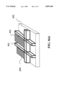
- FIG. 5 is a diagram illustrating the BSE process for fabricating the cruciform bump shown in FIG. 4.
- the ultraviolet (UV) light 501 illuminates from the back side of the TFT substrate 402. Since the metal electrodes 502 on the TFT substrate 402 are opaque, the bump structure 504 on the bus line 503 is constructed on the top of these non-transparent metal bus lines by a standard photo-lithographic process. This process is accomplished by means of self-aligned exposure without using a photomask.
- FIG. 6 shows the side view of the novel structure and the operation mechanism of a multi-domain homeotropic aligned liquid crystal display according to the invention.
- the alignment films 601 and 602 are printed on a common electrode 609 of a top color filter substrate 603 and the metal electrode 502 of the bottom TFT substrate 402 respectively.
- nematic liquid crystal is injected into the cell.
- the liquid crystal directors are perpendicularly anchored on the boundaries of the bump structure 504. High pre-tilt angle around the pixel is introduced by the bump structure 504 without using rubbing process.
- the homeotropical aligned liquid crystals do not modulate the polarization of incident light.
- the liquid crystal molecules 604 are perpendicular to the electrode when the applied voltage is off (OFF state) as shown in the right hand side of FIG. 6. Since the LCD is sandwiched between crossed polarizers 605 and 605', the dark state is perfectly dark.
- the compensators A-plate 606 and C-plate 607 are necessary for a homeotropical aligned LCD to eliminate the angular dependence of a dark state.
- the directors of liquid crystal molecules are reoriented and the liquid crystal molecules 608 are parallel to the electrode.
- the tilt directions are determined by the combination effect of a fringe field and the bump structure.
- the light intensity is modulated by the crossed polarizers due to the liquid crystal directors' field.
- FIG. 7a shows the optical texture when the absorbing axis 701 and 702 of crossed polarizers of a multi-domain homeotropic aligned liquid crystal display of the present invention are placed at ⁇ 45° directions respectively with a voltage being applied.
- the shape of the pixel 703 in the left figure of FIG. 7a is quasi-square.
- the bump 704 is formed around the pixel electrode.
- the optical texture of the light transmitted region 705 changes from full dark to disclination texture 706.
- the pixel shape in the right figure of FIG. 7a is quasi-rectangle.
- FIG. 7b shows the optical texture when the absorbing axis 707 and 708 of crossed polarizers are placed at 0° and 90° directions respectively with a voltage being applied.
- the pixel shape in the left figure is quasi-square while the pixel shape in the right figure is quasi-rectangle.
- the disinclination texture in FIG. 7 is changed by the voltage applied. When a larger voltage is applied, the disinclination texture becomes narrower and the intensity also gets higher.
- the bump structure shown in FIG. 4 can be formed by utilizing the BSE method without rubbing process and polymer stabilized process. It is simpler and cheaper than using a standard photo-lithographic procedure. Because it saves one photo-lithographic procedure, the problems of misalignment, smaller process window and possibly sacrificing the aperture ratio are all eliminated.
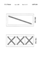
- plural openings are further formed on pixel electrodes or common electrodes in order to obtain high quality images for the LCD display.
- the openings are preferably formed on the common electrodes.
- Standard photo-lithographic process can be used to fabricate the electrodes with openings.
- the pattern of the openings on the electrodes determines the characteristics of the multi-domain LCD cells.
- the shape of the opening patterns may be double-Y, X, multiple Xs, diagonal slot, vertical slot or multiple horizontal slots according to the invention.
- FIGS. 8(a)-8(f) illustrate these opening patterns respectively.
- the pixels may be arranged as a rectangle or square. It may also be mosaic arrangement.
- the vertical slot opening at the central portion is disposed in parallel with the longer sides of the pixel and perpendicular to the shorter sides.
- the horizontal slot opening is disposed in parallel with the shorter sides of the pixel and perpendicular to the longer sides of the pixel.
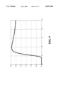
- FIG. 9 shows the voltage-dependent transmittance curve in a multi-domain homeotropic aligned liquid crystal display with cruciform bump structure formed using the BSE method according to the invention.
- the liquid crystal directors in off state are perpendicularly aligned to the substrates and the boundaries of the bump structure.
- the multi-domain homeotropic aligned liquid crystal display panels are operated in normally-black mode. The shimmer around the bumps is blocked by the black matrix to ensure that the dark state is perfectly dark.
- the transmittance is very low when the applied voltages are smaller than the threshold voltage of 2.3 volts as shown in FIG. 9.
- the aperture ratio of the LCD is around 47%. It can reach up to 2.9% transmittance when a voltage of 5 volts is applied. This is about 55% light intensity of a conventional 90°-twisted nematic LCD, and is 20% higher than that of a conventional vertically aligned wide-viewing angle LCD.
- FIG. 10 shows the optical response in a multi-domain homeotropic aligned liquid crystal display according to the invention.
- the response is measured by switching the voltage between 0 and 5 volts.
- the rise time (10% to 90% of transmittance difference between 0 and 5 volts) is about 17 ms and the decay time (90% to 10% of transmittance difference between 0 and 5 volts) is about 11.5 ms.
- the total response time is about 28.5 ms which is fast enough for its applications.
- FIG. 11 shows the response between the gray levels in the multi-domain homeotropic aligned liquid crystal display of the present invention.
- the transmittance between 0 and 5 volts is divided into 8 gray levels, from level 0 to level 7.
- line segments connected by square dots represent the rise time of switching from gray levels 1 ⁇ 6 to level 7 while line segments connected by circular dots represent the rise time of switching from gray levels 1 ⁇ 5 to level 6.
- the rise time of switching from gray levels 1 ⁇ 6 to level 7 (5 volts) is less than 11 ms, and 16.5 ms for gray levels 1 ⁇ 5 to level 6.
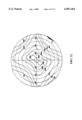
- FIG. 12 shows the iso-contrast contours of a multi-domain homeotropic aligned liquid crystal display according to the invention with compensator A- and C-plates. Both compensation films are commercialized products.
- FIG. 13 shows the colorimetry in a multi-domain homeotropic aligned liquid crystal display according to the invention. The results are measured at white level at 70° in all azimuthal angles.
- the horseshoe-shaped area is the distribution range of the wavelength of visible light.
- point (0.313, 0.329) in CIE coordinate as the standard light source D65
- the rectangular area from (0.335, 0.34) to (0.355, 0.37) is enlarged and shown at the upper-right corner of FIG. 13.
- the range of the colorimetry is dense and closed to the standard light source D65. It means that the color dispersion is very small (0.018 in this embodiment) and the color of the white level will be independent of the viewing angle.
- the color dispersion is much less than that of a conventional 90°-twisted nematic LCD or a wide-viewing angle inplane switch (IPS) LCD. Therefore, the multi-domain homeotropic aligned LCD of the invention shows uniform color performance which is induced by the quasi-symmetric director field.
- IPS inplane switch
Abstract
Description
Claims (29)
Applications Claiming Priority (2)
| Application Number | Priority Date | Filing Date | Title |
|---|---|---|---|
| TW088120131 | 1999-11-18 | ||
| TW088120131A TW548475B (en) | 1999-11-18 | 1999-11-18 | Fabrication method of homeotropic aligned LCD structure and the bump structure |
Publications (1)
| Publication Number | Publication Date |
|---|---|
| US6097464A true US6097464A (en) | 2000-08-01 |
Family
ID=21643069
Family Applications (1)
| Application Number | Title | Priority Date | Filing Date |
|---|---|---|---|
| US09/484,395 Expired - Lifetime US6097464A (en) | 1999-11-18 | 2000-01-14 | Multi-domain homeotropic aligned liquid crystal display having cruciform bumps formed around pixel electrodes |
Country Status (3)
| Country | Link |
|---|---|
| US (1) | US6097464A (en) |
| JP (1) | JP2001154200A (en) |
| TW (1) | TW548475B (en) |
Cited By (38)
| Publication number | Priority date | Publication date | Assignee | Title |
|---|---|---|---|---|
| US6256080B1 (en) * | 1999-06-23 | 2001-07-03 | International Business Machines Corporation | Self-aligned structures for improved wide viewing angle for liquid crystal displays |
| US6313899B1 (en) * | 1999-08-05 | 2001-11-06 | Chi Mei Electronics Corporation | Homeotropic liquid crystal display with protrusions comprising additional electrodes |
| US20010040546A1 (en) * | 1998-12-08 | 2001-11-15 | Fujitsu Limited | Liquid crystal display device and its drive method |
| US20020036740A1 (en) * | 2000-08-11 | 2002-03-28 | Masumi Kubo | Liquid crystal display device |
| WO2002042839A1 (en) * | 2000-11-21 | 2002-05-30 | Konovalov Victor A | Multidomain liquid crystal display and method for manufacturing thereof |
| US6476896B1 (en) * | 2000-03-07 | 2002-11-05 | Industrial Technology Research Institute | Structure of a multi-domain wide viewing angle liquid crystal display |
| US20020167278A1 (en) * | 2001-05-11 | 2002-11-14 | Sunghoe Yoon | Reflective cholesteric liquid crystal display device and manufacturing method for the same |
| US6549257B2 (en) * | 2000-05-22 | 2003-04-15 | Industrial Technology Research Institute | Structure of a multi-domain wide viewing angle liquid crystal display |
| US6573965B1 (en) * | 2000-05-12 | 2003-06-03 | Industrial Technology Research Institute | Multi-domain wide viewing angle liquid crystal display having slits on electrodes and bumps above the slits |
| US20030134506A1 (en) * | 2002-01-14 | 2003-07-17 | Plasmion Corporation | Plasma display panel having trench discharge cell and method of fabricating the same |
| US6633356B1 (en) * | 1998-10-12 | 2003-10-14 | Fujitsu Limited | Liquid crystal display and method for fabricating the same |
| US6667241B2 (en) * | 2001-04-04 | 2003-12-23 | Au Optronics Corp. | Process for manufacturing reflective TFT-LCD with slant diffusers |
| US6710833B2 (en) * | 2000-06-30 | 2004-03-23 | Hannstar Display Corporation | Multi-domain vertical alignment liquid crystal display with wide viewing angle |
| US20040057002A1 (en) * | 1999-02-12 | 2004-03-25 | Matsushita Electric Industrial Co., Ltd. | Liquid crystal element and manufacturing method thereof |
| US20040155998A1 (en) * | 2000-10-31 | 2004-08-12 | Sharp Kabushiki Kaisha | Liquid crystal display device |
| US20040201807A1 (en) * | 2002-11-01 | 2004-10-14 | Kopin Corporation | Multi-domain vertical alignment liquid crystal display |
| US20040246423A1 (en) * | 2003-03-20 | 2004-12-09 | Fujitsu Display Technologies Corporation | Liquid crystal display apparatus and manufacturing method therefor |
| US20050168674A1 (en) * | 2004-02-02 | 2005-08-04 | Sharp Kabushiki Kaisha | Liquid crystal display device |
| US20050270457A1 (en) * | 2004-05-21 | 2005-12-08 | Kopin Corporation | Full symmetrical wide-viewing angle display |
| US20060066793A1 (en) * | 2004-09-24 | 2006-03-30 | Fujitsu Display Technologies Corporation | Liquid crystal display device |
| US7072017B1 (en) * | 2000-06-29 | 2006-07-04 | Lg. Philips Lcd Co., Ltd. | Multi-domain liquid crystal display device having a common-auxiliary electrode and dielectric structures |
| US20060274246A1 (en) * | 2000-03-31 | 2006-12-07 | Sharp Kabushiki Kaisha | Liquid crystal display device |
| US20060279682A1 (en) * | 2003-04-04 | 2006-12-14 | Samsung Electronic Co., Ltd. | Liquid crystal display and thin film transistor panel therefor |
| US20070052898A1 (en) * | 2005-04-18 | 2007-03-08 | Wintek Corporation | Multi-domain structure of wide-view-angle liquid crystal displays |
| CN100339745C (en) * | 2002-06-29 | 2007-09-26 | 京东方显示器科技公司 | Vertical orientation mode liquid crystal display device |
| US7292300B2 (en) | 2000-10-31 | 2007-11-06 | Sharp Kabushiki Kaisha | Liquid crystal display with radially-inclined liquid crystal in unit solid portions arranged in a single direction |
| US7375781B2 (en) | 2003-12-24 | 2008-05-20 | Sharp Kabushiki Kaisha | Liquid crystal display device |
| US7499136B2 (en) | 2004-04-26 | 2009-03-03 | Sharp Kabushiki Kaisha | Liquid crystal display device |
| CN100495168C (en) * | 2001-10-02 | 2009-06-03 | 夏普株式会社 | Substrate for liquid crystal display, and liquid crystal display using the same |
| US20090237605A1 (en) * | 2008-03-18 | 2009-09-24 | Seiko Epson Corporation | Liquid crystal device and electronic apparatus |
| US20090316096A1 (en) * | 2000-06-20 | 2009-12-24 | Alessandro Cesare Callegari | Multi-domain and ips liquid-crystal display using dry alignment |
| US20100060813A1 (en) * | 2006-12-18 | 2010-03-11 | Yuki Kawashima | Liquid crystal display |
| US20100118227A1 (en) * | 2007-03-28 | 2010-05-13 | Satoshi Shibata | Liquid cystal display panel with microlens array and method for manufacturing the same |
| US8111356B2 (en) | 2006-09-12 | 2012-02-07 | Sharp Kabushiki Kaisha | Liquid crystal display panel provided with microlens array, method for manufacturing the liquid crystal display panel, and liquid crystal display device |
| US8174641B2 (en) | 2006-09-28 | 2012-05-08 | Sharp Kabushiki Kaisha | Liquid crystal display panel with microlens array, its manufacturing method, and liquid crystal display device |
| US8300188B2 (en) | 2007-01-11 | 2012-10-30 | Sharp Kabushiki Kaisha | Liquid crystal display panel with micro-lens array and liquid crystal display device |
| US8546808B2 (en) | 2000-08-11 | 2013-10-01 | Sharp Kabushiki Kaisha | Liquid crystal display device |
| US10541233B2 (en) * | 2017-12-22 | 2020-01-21 | Industrial Technology Research Institute | Display device |
Families Citing this family (8)
| Publication number | Priority date | Publication date | Assignee | Title |
|---|---|---|---|---|
| JP4837269B2 (en) * | 2000-08-11 | 2011-12-14 | シャープ株式会社 | Liquid crystal display |
| JP3875125B2 (en) * | 2001-04-11 | 2007-01-31 | シャープ株式会社 | Liquid crystal display |
| JP3944649B2 (en) | 2003-04-21 | 2007-07-11 | セイコーエプソン株式会社 | Liquid crystal display device and electronic device |
| JP4720139B2 (en) * | 2004-09-30 | 2011-07-13 | ソニー株式会社 | LCD panel |
| KR20060059089A (en) * | 2004-11-26 | 2006-06-01 | 삼성에스디아이 주식회사 | Liquid crystal display comprising ocb mode liquid crystal layer and fabrication method of the same |
| JP4830468B2 (en) * | 2005-11-30 | 2011-12-07 | ソニー株式会社 | LCD panel |
| TWI437331B (en) * | 2010-06-25 | 2014-05-11 | Innolux Corp | Liquid crystal display device |
| TWI414768B (en) * | 2011-06-10 | 2013-11-11 | Benq Materials Corp | Detecting method and system for 3d micro-retardation film |
Citations (3)
| Publication number | Priority date | Publication date | Assignee | Title |
|---|---|---|---|---|
| US5309264A (en) * | 1992-04-30 | 1994-05-03 | International Business Machines Corporation | Liquid crystal displays having multi-domain cells |
| US5737051A (en) * | 1992-09-18 | 1998-04-07 | Hitachi, Ltd. | Liquid crystal display device |
| US5914761A (en) * | 1993-09-20 | 1999-06-22 | Hitachi, Ltd. | Liquid crystal display device with at least one of insulating layer and orienting film |
-
1999
- 1999-11-18 TW TW088120131A patent/TW548475B/en not_active IP Right Cessation
-
2000
- 2000-01-14 US US09/484,395 patent/US6097464A/en not_active Expired - Lifetime
- 2000-03-06 JP JP2000060241A patent/JP2001154200A/en active Pending
Patent Citations (3)
| Publication number | Priority date | Publication date | Assignee | Title |
|---|---|---|---|---|
| US5309264A (en) * | 1992-04-30 | 1994-05-03 | International Business Machines Corporation | Liquid crystal displays having multi-domain cells |
| US5737051A (en) * | 1992-09-18 | 1998-04-07 | Hitachi, Ltd. | Liquid crystal display device |
| US5914761A (en) * | 1993-09-20 | 1999-06-22 | Hitachi, Ltd. | Liquid crystal display device with at least one of insulating layer and orienting film |
Non-Patent Citations (12)
| Title |
|---|
| ASIA Display 98, 375 Wide Viewing Angle TFT LCD Based on Rdge and Fringe Field Multi Domain Homeotropic Structure, 1998. * |
| ASIA Display 98, 375 Wide Viewing Angle TFT-LCD Based on Rdge and Fringe-Field Multi-Domain Homeotropic Structure, 1998. |
| ASIA Display 98.375 LCD Wide Viewing Angle TFT LCD Based on Ridge and Fringe Field Multi Domain Homeotropic Structure. * |
| ASIA Display 98.375 LCD Wide Viewing Angle TFT-LCD Based on Ridge and Fringe-Field Multi-Domain Homeotropic Structure. |
| SID 98 Digest. 1998 Ridge and Fringe Field Multi Domain Homeotropic. * |
| SID 98 Digest. 1998 Ridge and Fringe-Field Multi-Domain Homeotropic. |
| SID 98 Digest. A Super High Image Quality Multi Domain Vertical Alignment LCD by New Rubbing Less Technology, 1998. * |
| SID 98 Digest. A Super-High-Image-Quality Multi-Domain Vertical Alignment LCD by New Rubbing-Less Technology, 1998. |
| SID 98 Digest. Ridge and Fringe Field Multi Domain Homeotropic LCD, 1998. * |
| SID 98 Digest. Ridge and Fringe-Field Multi-Domain Homeotropic LCD, 1998. |
| SID 98Digest. 1077 1080 1998 A Super Hight Image Quality Multi Domain Vertical Alignment LCD. * |
| SID 98Digest. 1077-1080 1998 A Super-Hight-Image-Quality Multi-Domain Vertical Alignment LCD. |
Cited By (73)
| Publication number | Priority date | Publication date | Assignee | Title |
|---|---|---|---|---|
| US6633356B1 (en) * | 1998-10-12 | 2003-10-14 | Fujitsu Limited | Liquid crystal display and method for fabricating the same |
| US7532183B2 (en) | 1998-12-08 | 2009-05-12 | Sharp Kabushiki Kaisha | Liquid crystal display device and its drive method |
| US20090190050A1 (en) * | 1998-12-08 | 2009-07-30 | Sharp Kabushiki Kaisha | Liquid crystal display device and its drive method |
| US20010040546A1 (en) * | 1998-12-08 | 2001-11-15 | Fujitsu Limited | Liquid crystal display device and its drive method |
| US20060017677A1 (en) * | 1998-12-08 | 2006-01-26 | Sharp Kabushiki Kaisha | Liquid crystal display device and its drive method |
| US6952192B2 (en) * | 1998-12-08 | 2005-10-04 | Sharp Kabushiki Kaisha | Liquid crystal display device and its drive method |
| US7230666B2 (en) * | 1999-02-12 | 2007-06-12 | Matsushita Electric Industrial Co., Ltd. | Liquid crystal display with nonconductive portions in specific areas |
| US20040057002A1 (en) * | 1999-02-12 | 2004-03-25 | Matsushita Electric Industrial Co., Ltd. | Liquid crystal element and manufacturing method thereof |
| US6256080B1 (en) * | 1999-06-23 | 2001-07-03 | International Business Machines Corporation | Self-aligned structures for improved wide viewing angle for liquid crystal displays |
| US6313899B1 (en) * | 1999-08-05 | 2001-11-06 | Chi Mei Electronics Corporation | Homeotropic liquid crystal display with protrusions comprising additional electrodes |
| US6476896B1 (en) * | 2000-03-07 | 2002-11-05 | Industrial Technology Research Institute | Structure of a multi-domain wide viewing angle liquid crystal display |
| US20060274246A1 (en) * | 2000-03-31 | 2006-12-07 | Sharp Kabushiki Kaisha | Liquid crystal display device |
| US7167222B2 (en) * | 2000-03-31 | 2007-01-23 | Sharp Kabushiki Kaisha | Liquid crystal display with antiglare layer on viewer side having haze equal to or greater than 40 |
| US6573965B1 (en) * | 2000-05-12 | 2003-06-03 | Industrial Technology Research Institute | Multi-domain wide viewing angle liquid crystal display having slits on electrodes and bumps above the slits |
| US6549257B2 (en) * | 2000-05-22 | 2003-04-15 | Industrial Technology Research Institute | Structure of a multi-domain wide viewing angle liquid crystal display |
| US20090316096A1 (en) * | 2000-06-20 | 2009-12-24 | Alessandro Cesare Callegari | Multi-domain and ips liquid-crystal display using dry alignment |
| US7072017B1 (en) * | 2000-06-29 | 2006-07-04 | Lg. Philips Lcd Co., Ltd. | Multi-domain liquid crystal display device having a common-auxiliary electrode and dielectric structures |
| US6710833B2 (en) * | 2000-06-30 | 2004-03-23 | Hannstar Display Corporation | Multi-domain vertical alignment liquid crystal display with wide viewing angle |
| US8546808B2 (en) | 2000-08-11 | 2013-10-01 | Sharp Kabushiki Kaisha | Liquid crystal display device |
| US20060278874A1 (en) * | 2000-08-11 | 2006-12-14 | Sharp Kabushiki Kaisha | Liquid crystal display device |
| US20100157182A1 (en) * | 2000-08-11 | 2010-06-24 | Sharp Kabushiki Kaisha | Liquid crystal display device |
| US7755087B2 (en) | 2000-08-11 | 2010-07-13 | Sharp Kabushiki Kaisha | Liquid crystal display device with sub-picture element electrodes electrically separated from each other |
| US20040201810A1 (en) * | 2000-08-11 | 2004-10-14 | Sharp Kabushiki Kaisha | Liquid crystal display device |
| US8053775B2 (en) | 2000-08-11 | 2011-11-08 | Sharp Kabushiki Kaisha | Liquid crystal display device |
| US20020036740A1 (en) * | 2000-08-11 | 2002-03-28 | Masumi Kubo | Liquid crystal display device |
| US7215395B2 (en) | 2000-08-11 | 2007-05-08 | Sharp Kabushiki Kaisha | Liquid crystal display device |
| US7145624B2 (en) * | 2000-08-11 | 2006-12-05 | Sharp Kabushiki Kaisha | Liquid crystal display device having multiple domains with radially inclined LC molecules |
| US7292300B2 (en) | 2000-10-31 | 2007-11-06 | Sharp Kabushiki Kaisha | Liquid crystal display with radially-inclined liquid crystal in unit solid portions arranged in a single direction |
| US6862062B2 (en) | 2000-10-31 | 2005-03-01 | Sharp Kabushiki Kaisha | Liquid crystal display device |
| US7532291B2 (en) | 2000-10-31 | 2009-05-12 | Sharp Kabushiki Kaisha | Liquid crystal display device |
| US7230664B2 (en) * | 2000-10-31 | 2007-06-12 | Sharp Kabushiki Kaisha | Liquid crystal display device |
| US20040155998A1 (en) * | 2000-10-31 | 2004-08-12 | Sharp Kabushiki Kaisha | Liquid crystal display device |
| US20070139594A1 (en) * | 2000-10-31 | 2007-06-21 | Sharp Kabushiki Kaisha, Osaka, Japan | Liquid crystal display device |
| WO2002042839A1 (en) * | 2000-11-21 | 2002-05-30 | Konovalov Victor A | Multidomain liquid crystal display and method for manufacturing thereof |
| US6667241B2 (en) * | 2001-04-04 | 2003-12-23 | Au Optronics Corp. | Process for manufacturing reflective TFT-LCD with slant diffusers |
| US20020167278A1 (en) * | 2001-05-11 | 2002-11-14 | Sunghoe Yoon | Reflective cholesteric liquid crystal display device and manufacturing method for the same |
| US7196752B2 (en) * | 2001-05-11 | 2007-03-27 | L.G.Philips Lcd Co., Ltd. | Cholesteric liquid crystal color filter with protrusions and associated methods of manufacture |
| CN100495168C (en) * | 2001-10-02 | 2009-06-03 | 夏普株式会社 | Substrate for liquid crystal display, and liquid crystal display using the same |
| US6897564B2 (en) | 2002-01-14 | 2005-05-24 | Plasmion Displays, Llc. | Plasma display panel having trench discharge cells with one or more electrodes formed therein and extended to outside of the trench |
| US20030134506A1 (en) * | 2002-01-14 | 2003-07-17 | Plasmion Corporation | Plasma display panel having trench discharge cell and method of fabricating the same |
| CN100339745C (en) * | 2002-06-29 | 2007-09-26 | 京东方显示器科技公司 | Vertical orientation mode liquid crystal display device |
| US20040201807A1 (en) * | 2002-11-01 | 2004-10-14 | Kopin Corporation | Multi-domain vertical alignment liquid crystal display |
| US9091886B2 (en) * | 2003-03-20 | 2015-07-28 | Sharp Kabushiki Kaisha | Liquid crystal display apparatus wherein alignment control layers and bumps are made of a polymerizable compound included in and mixed with a liquid crystal layer |
| US20070152221A1 (en) * | 2003-03-20 | 2007-07-05 | Takashi Sasabayashi | Liquid crystal display apparatus and manufacturing method therefor |
| US7910924B2 (en) | 2003-03-20 | 2011-03-22 | Sharp Kabushiki Kaisha | Liquid crystal display apparatus and manufacturing method therefor |
| US20040246423A1 (en) * | 2003-03-20 | 2004-12-09 | Fujitsu Display Technologies Corporation | Liquid crystal display apparatus and manufacturing method therefor |
| US20120220181A1 (en) * | 2003-03-20 | 2012-08-30 | Sharp Kabushiki Kaisha | Liquid crystal display apparatus and manufacturing method therefor |
| US7253438B2 (en) * | 2003-03-20 | 2007-08-07 | Sharp Kabushiki Kaisha | Liquid crystal display apparatus and manufacturing method therefor |
| US20110090441A1 (en) * | 2003-03-20 | 2011-04-21 | Sharp Kabushiki Kaisha | Liquid crystal display apparatus and manufacturing method therefor |
| US8202748B2 (en) | 2003-03-20 | 2012-06-19 | Sharp Kabushiki Kaisha | Liquid crystal display apparatus and manufacturing method therefor |
| US7675597B2 (en) | 2003-04-04 | 2010-03-09 | Samsung Electronics Co., Ltd. | Liquid crystal display and thin film transistor panel therefor |
| US8149366B2 (en) | 2003-04-04 | 2012-04-03 | Samsung Electronics Co., Ltd. | Liquid crystal display and thin film transistor panel therefor |
| US20100009479A1 (en) * | 2003-04-04 | 2010-01-14 | Dong-Gyu Kim | Liquid crystal display and thin film transistor panel therefor |
| US7667806B2 (en) * | 2003-04-04 | 2010-02-23 | Samsung Electronics Co., Ltd. | Liquid crystal display and thin film transistor panel therefor |
| US20060279682A1 (en) * | 2003-04-04 | 2006-12-14 | Samsung Electronic Co., Ltd. | Liquid crystal display and thin film transistor panel therefor |
| US20060285049A1 (en) * | 2003-04-04 | 2006-12-21 | Samsung Electronic Co., Ltd. | Liquid crystal display and thin film transistor panel therefor |
| US7375781B2 (en) | 2003-12-24 | 2008-05-20 | Sharp Kabushiki Kaisha | Liquid crystal display device |
| US20050168674A1 (en) * | 2004-02-02 | 2005-08-04 | Sharp Kabushiki Kaisha | Liquid crystal display device |
| US7379137B2 (en) | 2004-02-02 | 2008-05-27 | Sharp Kabushiki Kaisha | Liquid crystal display device |
| US7499136B2 (en) | 2004-04-26 | 2009-03-03 | Sharp Kabushiki Kaisha | Liquid crystal display device |
| US20050270457A1 (en) * | 2004-05-21 | 2005-12-08 | Kopin Corporation | Full symmetrical wide-viewing angle display |
| US7564522B2 (en) | 2004-05-21 | 2009-07-21 | Kopin Corporation | Full symmetrical wide-viewing angle display |
| US20060066793A1 (en) * | 2004-09-24 | 2006-03-30 | Fujitsu Display Technologies Corporation | Liquid crystal display device |
| US20070052898A1 (en) * | 2005-04-18 | 2007-03-08 | Wintek Corporation | Multi-domain structure of wide-view-angle liquid crystal displays |
| US8111356B2 (en) | 2006-09-12 | 2012-02-07 | Sharp Kabushiki Kaisha | Liquid crystal display panel provided with microlens array, method for manufacturing the liquid crystal display panel, and liquid crystal display device |
| US8174641B2 (en) | 2006-09-28 | 2012-05-08 | Sharp Kabushiki Kaisha | Liquid crystal display panel with microlens array, its manufacturing method, and liquid crystal display device |
| US8068201B2 (en) | 2006-12-18 | 2011-11-29 | Sharp Kabushiki Kaisha | Liquid crystal display having particular auxiliary electrode |
| US20100060813A1 (en) * | 2006-12-18 | 2010-03-11 | Yuki Kawashima | Liquid crystal display |
| US8300188B2 (en) | 2007-01-11 | 2012-10-30 | Sharp Kabushiki Kaisha | Liquid crystal display panel with micro-lens array and liquid crystal display device |
| US20100118227A1 (en) * | 2007-03-28 | 2010-05-13 | Satoshi Shibata | Liquid cystal display panel with microlens array and method for manufacturing the same |
| US8164725B2 (en) * | 2008-03-18 | 2012-04-24 | Seiko Epson Corporation | Liquid crystal device and electronic apparatus |
| US20090237605A1 (en) * | 2008-03-18 | 2009-09-24 | Seiko Epson Corporation | Liquid crystal device and electronic apparatus |
| US10541233B2 (en) * | 2017-12-22 | 2020-01-21 | Industrial Technology Research Institute | Display device |
Also Published As
| Publication number | Publication date |
|---|---|
| TW548475B (en) | 2003-08-21 |
| JP2001154200A (en) | 2001-06-08 |
Similar Documents
| Publication | Publication Date | Title |
|---|---|---|
| US6097464A (en) | Multi-domain homeotropic aligned liquid crystal display having cruciform bumps formed around pixel electrodes | |
| US8253908B2 (en) | Liquid crystal display | |
| US7227606B2 (en) | Vertically-alligned (VA) liquid crystal display device | |
| US6256080B1 (en) | Self-aligned structures for improved wide viewing angle for liquid crystal displays | |
| US6384889B1 (en) | Liquid crystal display with sub pixel regions defined by sub electrode regions | |
| US8049848B2 (en) | Liquid crystal display and method of manufacturing the same and method of driving the same | |
| US8189152B2 (en) | Production method of liquid crystal display device and liquid crystal display device | |
| US7440061B2 (en) | In-plane switching LCD panel | |
| US6400440B1 (en) | Passive liquid crystal display having pre-tilt control structure and light absorbent material at a center | |
| US6549257B2 (en) | Structure of a multi-domain wide viewing angle liquid crystal display | |
| US8035784B2 (en) | Semi-transmissive liquid crystal display device and manufacturing method of the same | |
| US20060255337A1 (en) | Multi-domain member for a display device | |
| US6476896B1 (en) | Structure of a multi-domain wide viewing angle liquid crystal display | |
| US6593988B1 (en) | Multi-domain liquid crystal display with wall-bump structures in pixel area | |
| JP3400403B2 (en) | Liquid crystal display | |
| US11150520B2 (en) | Liquid crystal display device | |
| JPH0829790A (en) | Liquid crystal display device | |
| US7369197B2 (en) | Polarizer, panel for a liquid crystal display, and liquid crystal display, including a scattering layer | |
| JP2005189476A (en) | Liquid crystal display device | |
| JPH09318960A (en) | Liquid crystal display device | |
| JP2004094274A (en) | Liquid crystal display device and its manufacturing method as well as its driving method | |
| JP2001021868A (en) | Manufacture of liquid crystal display element |
Legal Events
| Date | Code | Title | Description |
|---|---|---|---|
| AS | Assignment |
Owner name: INDUSTRIAL TECHNOLOGY RESEARCH INSTITUTE, TAIWAN Free format text: ASSIGNMENT OF ASSIGNORS INTEREST;ASSIGNOR:LIU, HONG-DA;REEL/FRAME:010509/0216 Effective date: 20000103 |
|
| STCF | Information on status: patent grant |
Free format text: PATENTED CASE |
|
| AS | Assignment |
Owner name: AU OPTRONICS CORP., TAIWAN Free format text: ASSIGNMENT OF ASSIGNORS INTEREST;ASSIGNOR:INDUSTRIAL TECHNOLOGY RESEARCH INSTITUTE;REEL/FRAME:013740/0654 Effective date: 20020724 Owner name: CHI MEI OPTOELECTRONICS CORP., TAIWAN Free format text: ASSIGNMENT OF ASSIGNORS INTEREST;ASSIGNOR:INDUSTRIAL TECHNOLOGY RESEARCH INSTITUTE;REEL/FRAME:013740/0654 Effective date: 20020724 Owner name: CHUNGHWA PICTURE TUBES, LTD., TAIWAN Free format text: ASSIGNMENT OF ASSIGNORS INTEREST;ASSIGNOR:INDUSTRIAL TECHNOLOGY RESEARCH INSTITUTE;REEL/FRAME:013740/0654 Effective date: 20020724 Owner name: HANNSTAR DISPLAY CORP., TAIWAN Free format text: ASSIGNMENT OF ASSIGNORS INTEREST;ASSIGNOR:INDUSTRIAL TECHNOLOGY RESEARCH INSTITUTE;REEL/FRAME:013740/0654 Effective date: 20020724 Owner name: INDUSTRIAL TECHNOLOGY RESEARCH INSTITUTE, TAIWAN Free format text: ASSIGNMENT OF ASSIGNORS INTEREST;ASSIGNOR:INDUSTRIAL TECHNOLOGY RESEARCH INSTITUTE;REEL/FRAME:013740/0654 Effective date: 20020724 Owner name: PRIME VIEW INTERNATIONAL CO., LTD., TAIWAN Free format text: ASSIGNMENT OF ASSIGNORS INTEREST;ASSIGNOR:INDUSTRIAL TECHNOLOGY RESEARCH INSTITUTE;REEL/FRAME:013740/0654 Effective date: 20020724 Owner name: QUANTA DISPLAY INC., TAIWAN Free format text: ASSIGNMENT OF ASSIGNORS INTEREST;ASSIGNOR:INDUSTRIAL TECHNOLOGY RESEARCH INSTITUTE;REEL/FRAME:013740/0654 Effective date: 20020724 Owner name: TOPPOLY OPTOELECTRONICS CORP., TAIWAN Free format text: ASSIGNMENT OF ASSIGNORS INTEREST;ASSIGNOR:INDUSTRIAL TECHNOLOGY RESEARCH INSTITUTE;REEL/FRAME:013740/0654 Effective date: 20020724 |
|
| FEPP | Fee payment procedure |
Free format text: PAYOR NUMBER ASSIGNED (ORIGINAL EVENT CODE: ASPN); ENTITY STATUS OF PATENT OWNER: LARGE ENTITY |
|
| FPAY | Fee payment |
Year of fee payment: 4 |
|
| FPAY | Fee payment |
Year of fee payment: 8 |
|
| REMI | Maintenance fee reminder mailed | ||
| AS | Assignment |
Owner name: INDUSTRIAL TECHNOLOGY RESEARCH INSTITUTE, TAIWAN Free format text: ASSIGNMENT OF ASSIGNORS INTEREST;ASSIGNORS:INDUSTRIAL TECHNOLOGY RESEARCH INSTITUTE;AU OPTRONICS CORP.;CHUNGHWA PICTURE TUBES, LTD.;AND OTHERS;REEL/FRAME:023234/0930 Effective date: 20090520 |
|
| FPAY | Fee payment |
Year of fee payment: 12 |