US6094123A - Low profile surface mount chip inductor - Google Patents
Low profile surface mount chip inductor Download PDFInfo
- Publication number
- US6094123A US6094123A US09/160,978 US16097898A US6094123A US 6094123 A US6094123 A US 6094123A US 16097898 A US16097898 A US 16097898A US 6094123 A US6094123 A US 6094123A
- Authority
- US
- United States
- Prior art keywords
- winding
- extending
- portions
- inductive device
- recessed
- Prior art date
- Legal status (The legal status is an assumption and is not a legal conclusion. Google has not performed a legal analysis and makes no representation as to the accuracy of the status listed.)
- Expired - Lifetime
Links
- 238000004804 winding Methods 0.000 claims abstract description 44
- 230000001939 inductive effect Effects 0.000 claims abstract description 10
- 239000004020 conductor Substances 0.000 claims abstract description 4
- 229910000859 α-Fe Inorganic materials 0.000 claims description 7
- 239000000463 material Substances 0.000 claims description 4
- 229910010293 ceramic material Inorganic materials 0.000 claims description 3
- 239000000976 ink Substances 0.000 description 15
- 238000000034 method Methods 0.000 description 14
- 239000000919 ceramic Substances 0.000 description 12
- 239000000696 magnetic material Substances 0.000 description 10
- 230000008569 process Effects 0.000 description 10
- 239000010410 layer Substances 0.000 description 9
- 230000004907 flux Effects 0.000 description 5
- PXHVJJICTQNCMI-UHFFFAOYSA-N nickel Substances [Ni] PXHVJJICTQNCMI-UHFFFAOYSA-N 0.000 description 5
- XEEYBQQBJWHFJM-UHFFFAOYSA-N Iron Chemical compound [Fe] XEEYBQQBJWHFJM-UHFFFAOYSA-N 0.000 description 4
- 229910052802 copper Inorganic materials 0.000 description 4
- 239000010949 copper Substances 0.000 description 4
- RYGMFSIKBFXOCR-UHFFFAOYSA-N Copper Chemical compound [Cu] RYGMFSIKBFXOCR-UHFFFAOYSA-N 0.000 description 3
- 229910052759 nickel Inorganic materials 0.000 description 3
- 238000007747 plating Methods 0.000 description 3
- 239000002356 single layer Substances 0.000 description 3
- KDLHZDBZIXYQEI-UHFFFAOYSA-N Palladium Chemical compound [Pd] KDLHZDBZIXYQEI-UHFFFAOYSA-N 0.000 description 2
- 239000011230 binding agent Substances 0.000 description 2
- 238000000151 deposition Methods 0.000 description 2
- 229910052742 iron Inorganic materials 0.000 description 2
- 229910052751 metal Inorganic materials 0.000 description 2
- 239000002184 metal Substances 0.000 description 2
- 238000012986 modification Methods 0.000 description 2
- 230000004048 modification Effects 0.000 description 2
- 238000012545 processing Methods 0.000 description 2
- 239000002994 raw material Substances 0.000 description 2
- 238000007650 screen-printing Methods 0.000 description 2
- 238000013459 approach Methods 0.000 description 1
- 230000015572 biosynthetic process Effects 0.000 description 1
- 239000003990 capacitor Substances 0.000 description 1
- 230000008859 change Effects 0.000 description 1
- 229910052804 chromium Inorganic materials 0.000 description 1
- 239000011248 coating agent Substances 0.000 description 1
- 238000000576 coating method Methods 0.000 description 1
- 230000008021 deposition Effects 0.000 description 1
- 238000009713 electroplating Methods 0.000 description 1
- 238000004146 energy storage Methods 0.000 description 1
- 238000002955 isolation Methods 0.000 description 1
- 229910052748 manganese Inorganic materials 0.000 description 1
- 239000011572 manganese Substances 0.000 description 1
- WJZHMLNIAZSFDO-UHFFFAOYSA-N manganese zinc Chemical compound [Mn].[Zn] WJZHMLNIAZSFDO-UHFFFAOYSA-N 0.000 description 1
- 238000004519 manufacturing process Methods 0.000 description 1
- 239000013528 metallic particle Substances 0.000 description 1
- 238000001465 metallisation Methods 0.000 description 1
- 150000002739 metals Chemical class 0.000 description 1
- 238000009740 moulding (composite fabrication) Methods 0.000 description 1
- QELJHCBNGDEXLD-UHFFFAOYSA-N nickel zinc Chemical compound [Ni].[Zn] QELJHCBNGDEXLD-UHFFFAOYSA-N 0.000 description 1
- 229910052763 palladium Inorganic materials 0.000 description 1
- SWELZOZIOHGSPA-UHFFFAOYSA-N palladium silver Chemical compound [Pd].[Ag] SWELZOZIOHGSPA-UHFFFAOYSA-N 0.000 description 1
- 239000000843 powder Substances 0.000 description 1
- 238000004080 punching Methods 0.000 description 1
- 238000000926 separation method Methods 0.000 description 1
- 229910052710 silicon Inorganic materials 0.000 description 1
- 229910052709 silver Inorganic materials 0.000 description 1
- 239000004332 silver Substances 0.000 description 1
- 238000005245 sintering Methods 0.000 description 1
- 229910000679 solder Inorganic materials 0.000 description 1
- 239000000758 substrate Substances 0.000 description 1
- 239000000725 suspension Substances 0.000 description 1
- 229910052719 titanium Inorganic materials 0.000 description 1
- 238000012546 transfer Methods 0.000 description 1
- 229910052725 zinc Inorganic materials 0.000 description 1
- 239000011701 zinc Substances 0.000 description 1
- 229910052726 zirconium Inorganic materials 0.000 description 1
Images


Classifications
-
- H—ELECTRICITY
- H01—ELECTRIC ELEMENTS
- H01F—MAGNETS; INDUCTANCES; TRANSFORMERS; SELECTION OF MATERIALS FOR THEIR MAGNETIC PROPERTIES
- H01F17/00—Fixed inductances of the signal type
- H01F17/0006—Printed inductances
- H01F17/0033—Printed inductances with the coil helically wound around a magnetic core
-
- H—ELECTRICITY
- H01—ELECTRIC ELEMENTS
- H01F—MAGNETS; INDUCTANCES; TRANSFORMERS; SELECTION OF MATERIALS FOR THEIR MAGNETIC PROPERTIES
- H01F27/00—Details of transformers or inductances, in general
- H01F27/28—Coils; Windings; Conductive connections
- H01F27/29—Terminals; Tapping arrangements for signal inductances
- H01F27/292—Surface mounted devices
Definitions
- This invention relates to inductors and in particular, to a low profile chip inductor for surface-mounting on a printed circuit board or metallized substrate.
- inductors perform a wide variety of essential functions in many electronic devices. For example, inductors are used in power supplies as choke coils, for energy storage and to minimize noise and AC ripple. Inductors are also used in transformers to change voltage level and to provide isolation.
- Inductors often comprise a magnetic core composed of an iron or ferrite material that is wound with a conductive coil. Consequently, inductors are often referred to as wire-wound coil devices.
- wire-wound coil devices One major difficulty with wire-wound coil devices is that they have relatively high-profiles which restrict miniaturization. While resistors, diodes, capacitors, and transistors have shrunk to the microscopic level, wire-wound coil devices remain bulky.
- conventional inductors is a particular problem in power circuits such as AC-DC and DC-DC power converters. Power converters remain bulky due, in large part, to the high profiles, large footprints, and high thermal resistances of the inductors and transformers. Furthermore, conventional inductors have a limited ability to transfer heat from the core and conductive windings to the device case or heat sink which necessitates larger surface areas for the entire circuit.
- An integral low profile inductive device comprises a magnetic body having opposing face surfaces, opposing side surfaces extending between the face surfaces, and opposing end surfaces extending between the side surfaces.
- a recessed surface is defined in each of the side surfaces of the body.
- An integral continuous winding of conductive material extends across the recessed surfaces and face surfaces of the body.
- Each of the recessed surfaces can be crenelated with alternating secondary recesses and projections such that the winding passes over the secondary recesses between the projections as it extends across the side surfaces or over the projections between the secondary recesses.
- the device can comprise one or more continuous windings each of at least one turn.
- FIG. 1 is a perspective view of a low-profile chip inductor according to the present invention
- FIG. 2 is a top plan view of the chip inductor of FIG. 1;
- FIG. 3 is a bottom plan view of the chip inductor of FIG. 1;
- FIG. 4 is a cross sectional view through line 4--4 FIG. 2;
- FIG. 5A is a perspective view of a low profile gapped U-core pair inductor or transformer assembled from two chip inductors;
- FIG. 5B is a schematic top plan view of the inductor or transformer of FIG. 5A;
- FIG. 6 is a schematic top plan view of a low profile E-core inductor or transformer assembled from three chip inductors;
- FIG. 7 is a schematic top plan view of a gapped toroid assembled from four chip inductors
- FIGS. 8A-8I depict a process for making the chip inductor of the present invention.
- FIGS. 9A-9D depict an alternative process for making the chip inductor of the present invention.
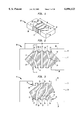
- FIGS. 1-3 show an integral low profile surface mountable chip inductor 10.
- the chip inductor 10 comprises a body 12 of magnetic material that is metallized with a coating of conductive material that defines a continuous conductive winding or coil 14.
- the winding 14 surrounds a portion 16 of the body 12 referred to as a core element.
- the side surfaces 18 of the body 12 in the area of the core element 16 include recessed crenelated surface portions 19 defined by alternating secondary recess surfaces 20 and projecting surfaces 22.
- the turns 24 of the winding 14 extend across the face surface 26, the mounting surface 30, and each side surface 18 of the body 12.
- the terminal ends 32 of the winding 14 are located on the mounting surface 30.
- Each terminal end 32 includes a rectangular contact pad 34 which permits the chip inductor 10 to electrically couple to various circuit elements associated with the board.
- the regions 35 where the windings approach the secondary recesses include rectangular contact pads which enable surface mounting and self-alignment with corresponding contact pads (not shown) on the board in a surface mount solder reflow operation.
- the winding 14 varies in width according to its location on the body 12.
- the portions of the winding 14 extending across the face and mounting surfaces 26, 30 have a maximum width that is larger than the width of the portions of the winding 14 extending across the side surfaces 18.
- the portion of the winding 14 extending across the side surfaces 18 pass over the secondary recess surfaces 20 such that they are separated by the non-metallized (insulating) projecting surfaces 22.
- the portion of the winding extending across the side surfaces 18 can pass over the projecting surfaces 22 so that they are separated by the secondary recess surfaces 20.
- FIGS. 1-3 show a case where the winding comprises 4 turns. More generally, the device comprises one or more windings each including one or more turns.
- FIG. 4 is a cross-sectional view through line 4--4 of FIG. 2.
- the body 12 of the chip inductor 10 can consist of multiple layers of magnetic material including an uppermost layer 40, an intermediate layer 42, and a lowermost layer 44.
- the body of the chip inductor may also include more than one intermediate layer and can also be constructed from a single layer of magnetic material if desired.
- FIG. 5A shows two of the chip inductors 10 surface-mounted side by side on a PC board 50 separated by a gap G and connected in series in a magnetic circuit producing a low profile gapped U-core pair inductor or transformer 52.
- FIG. 5B shows the magnetic flux path P U-core of this gapped U-core inductor or transformer pair. The magnetic flux path P U-core is confined within the bodies of the chips 10.
- FIG. 6 shows three of the chip inductors 10 surface-mounted side by side on a PC board 60 in a magnetic circuit to form a low profile E-core inductor or transformer 62. This device produces two magnetic flux paths P E-core which are confined within the bodies of the chips 10.
- FIG. 7 shows four of the chip inductors 10 mounted on a PC board 70 in a rectangular arrangement which produces a magnetic circuit 72 equivalent to a gapped toroid.
- the device 72 produces a magnetic flux path P torid which is confined within the bodies of the chips 10.
- magnetically coupled chip inductors can provide higher levels of inductance than a corresponding number of uncoupled chip inductors.
- FIGS. 8A-8J depict a multilayer green tape and thick film process for forming the chip inductors having bodies fabricated from at least one layer of magnetic material. The following process will be described as it relates to the fabrication of chip inductors having three layers of magnetic material.
- FIG. 8A shows one of three tape sections 80 of magnetic material used in fabricating the chip inductors.
- the tape section 80 of magnetic material is shown after paired rows 82 of vias 84 have been defined therein.
- the magnetic material used for making the tape sections 80 is selected from magnetic materials which can be metallized including but not limited to magnetic ceramics.
- the tape section 80 of magnetic material shown in FIG. 8A is composed of a green (unfired) magnetic ceramic material.
- the magnetic ceramic material may include a spinnel ferrite of the form M 1+x Fe 2-y O 4-z where the values for x, y, and z may assume both positive and negative numerical values.
- the M material typically includes at least one of the elements Mn, Ni, Zn, Fe, Cu, Co, Zr, Va, Cd, Ti, Cr, and Si.
- Exemplary ferrites are those ferrites which have high resistivities such as nickel-zinc ferrites and certain manganese-zinc ferrites.
- the ceramic raw materials (can be a single ceramic raw material) are provided in a powdered form.
- the ceramic powders are typically mixed with a suitable organic binder and cast in the form of a tape.
- the green ceramic tape is cut into a plurality of tape sections 80.
- forming and metallization processes can be performed on each individual tape section 80 or on a stacked group of tape sections which have been laminated together under low pressure in the range of 500 to 3,000 PSI at a temperature on the order of 50° C. to 100° C.
- the formation of multilayered ceramic bodies from green ceramic tapes is described in U.S. Pat. No. 5,239,744 to Fleming et al., the disclosure of which is incorporated herein by reference.
- the vias 84 defined in the ceramic tape section 80 extend from the top and bottom surfaces thereof and can possess the illustrated square geometry that produces four surfaces 86. Vias having circular geometries may also be used.
- the vias 84 can be created by punching the ceramic tape section 80 in a suitable punch press which uses a male punch corresponding to the size and shape of the via to be formed. Any technique capable of forming vias in a green ceramic tape can be used.
- FIG. 8B shows a layer of conductive ink 88 applied to the four surfaces 86 (FIG. 8A) of each of the vias 84 in the tape section 80.
- the conductive ink used may be a silver, a palladium, or a silver-palladium conductive ink.
- Such conductive inks are commercially available from many suppliers such as Ceronics Inc., Matawan, N.J.
- Conductive inks typically comprise a metallic particulate suspension in an organic binder, which can be applied using screenprinting techniques.
- the conductive ink is typically printed through a metal mask using vacuum suction to coat the surface or surfaces of each via 84.
- FIG. 8C shows each pairing of via rows 82 connected together by an elongated aperture 90 created in the tape section 80.
- the creation of the apertures 90 removes portions of the vias 84 in each row pair 82 thus, creating the crenelated recessed surfaces of the chip inductors.
- the conductive ink 88 applied to the remaining portions of the vias 84 will form the portions of the windings extending across the crenelated recessed surfaces of the chip inductors.
- registration holes (not shown) are typically formed in non-device areas of the tape sections 80. Registration rods (not shown) can then be inserted in the registration holes to assure alignment of the apertures 90 from each of the tape sections 80 when the tape sections 80 are later stacked.
- FIGS. 8A-8C are performed on each of the three tape sections. Two of the three tape sections 80 are then selected for further processing.
- FIG. 8D shows a pattern 94 of conductive ink screen printed onto one of the two selected green tape sections using a conductive ink similar to that applied to the vias 84.
- the pattern 94 shown in the figure defines the portions of the windings which span across the face surfaces of the chip inductors.
- FIG. 8E is a plan view of the entire tape section 94 after screen printing.
- a second pattern of conductive ink is printed onto the remaining one of the two selected tape sections (96 of FIG. 8F). This pattern defines the portions of the windings which span across the mounting surfaces of the chip inductors (includes the winding contact pads).
- the steps depicted in FIGS. 8D-8E are performed on only one side of the two selected tape sections.
- Tape sections used in single layer chip inductors are screen printed on both sides with respective portions of the winding pattern.
- the three tape sections 80, 92, 96 are stacked and laminated together into a mutilayered green laminate 100 as shown in FIG. 8F. (This step is omitted when making single layer chip inductors.)
- the tape sections 92, 96 with the face and mounted surface winding patterns are oriented in the stack so that they form the uppermost and lowermost tape sections of the laminate 100.
- FIG. 8G shows dicing lines 104 scribed into the green laminate 100 (only the uppermost tape section 92 of the laminate 100 is visible).
- the dicing lines 104 outline a plurality of discrete inductors 106 and facilitate their separation from each in later processing.
- the laminate 100 is sintered between 800° C. and 1400° C. This "co-fires" or densifies the ceramic tape sections 80, 92, 96 and the windings 102 of conductive ink. During sintering, the metallic particles in the conductive ink bond to the ceramic tape sections 80, 92, 96, to form a winding integral with the fired body.
- FIG. 8H shows the windings 102 of the co-fired laminate 100 after plating 108 with additional metals such as copper and nickel to increase the current carrying capacity of the windings 102.
- Copper plating may be performed by any plating technique with electrolytic plating being exemplary. This is accomplished by electrolytically depositing a layer of copper onto the windings of the laminate followed by the electrolytic or electroless deposition of nickel.
- FIG. 8I shows the multilayered laminate 100 being divided along the dice lines 104 to yield the plurality of discrete chip inductors 106.
- FIGS. 9A-9D depict an alternative process for making a chip inductor of the present invention.
- the alternative process is substantially similar to the process depicted in FIGS. 8A-8I, therefore, FIGS. 9A-9D illustrate only the differences.
- a single elongated via 112 is created in the green tape section 110 as shown in FIG. 9A.
- FIG. 9B shows a layer 116 of conductive ink applied to the four surfaces 114 of each of the elongated vias 112 in the tape section 110.
- FIG. 9C shows a plurality of spaced apart transverse apertures 118 are created in the tape section 110.
- the apertures 110 remove portions of each via 112 and defines the crenelated side surfaces of the body of the chip inductors.
- the conductive ink 116 in the remaining portions of each via 112 will form the portions of the windings extending across the crenelated recessed surfaces of the inductors.
- patterns 120 of conductive ink are screen printed onto two selected green tape sections 110 (only one shown).
- the patterns define the portions of the windings which span across the face and mounting surfaces of the inductors.
- the green tape sections 110 are stacked, diced, sintered, and singulated as described above.
Abstract
Description
Claims (8)
Priority Applications (3)
| Application Number | Priority Date | Filing Date | Title |
|---|---|---|---|
| US09/160,978 US6094123A (en) | 1998-09-25 | 1998-09-25 | Low profile surface mount chip inductor |
| EP99307284A EP0989568A3 (en) | 1998-09-25 | 1999-09-14 | Low profile surface mount chip inductor |
| JP11269666A JP2000114050A (en) | 1998-09-25 | 1999-09-24 | Surface mounting chip inductor with low profile |
Applications Claiming Priority (1)
| Application Number | Priority Date | Filing Date | Title |
|---|---|---|---|
| US09/160,978 US6094123A (en) | 1998-09-25 | 1998-09-25 | Low profile surface mount chip inductor |
Publications (1)
| Publication Number | Publication Date |
|---|---|
| US6094123A true US6094123A (en) | 2000-07-25 |
Family
ID=22579285
Family Applications (1)
| Application Number | Title | Priority Date | Filing Date |
|---|---|---|---|
| US09/160,978 Expired - Lifetime US6094123A (en) | 1998-09-25 | 1998-09-25 | Low profile surface mount chip inductor |
Country Status (3)
| Country | Link |
|---|---|
| US (1) | US6094123A (en) |
| EP (1) | EP0989568A3 (en) |
| JP (1) | JP2000114050A (en) |
Cited By (44)
| Publication number | Priority date | Publication date | Assignee | Title |
|---|---|---|---|---|
| US6342778B1 (en) * | 2000-04-20 | 2002-01-29 | Robert James Catalano | Low profile, surface mount magnetic devices |
| US6344784B1 (en) * | 1999-08-19 | 2002-02-05 | Murata Manufacturing Co., Ltd | Coil component |
| US6420954B1 (en) * | 1999-12-10 | 2002-07-16 | Micron Technology, Inc. | Coupled multilayer soft magnetic films for high frequency microtransformer for system-on-chip power supply |
| US20020095773A1 (en) * | 1999-07-09 | 2002-07-25 | Micron Technology, Inc. | Integrated circuit inductors |
| US20030057589A1 (en) * | 2000-11-09 | 2003-03-27 | Akihiko Ibata | Method of manufacturing ceramic material body |
| US20030074781A1 (en) * | 2001-10-23 | 2003-04-24 | Di/Dt, Inc. | Fully automatic process for magnetic circuit assembly |
| US20030079904A1 (en) * | 2001-10-03 | 2003-05-01 | Satoshi Sato | Electronic component and method of manufacturing the same |
| US20050052268A1 (en) * | 2003-09-05 | 2005-03-10 | Pleskach Michael D. | Embedded toroidal inductors |
| US20050128040A1 (en) * | 2003-12-15 | 2005-06-16 | Michael Gray | Magnetic assembly |
| US20050212642A1 (en) * | 2004-03-26 | 2005-09-29 | Harris Corporation | Embedded toroidal transformers in ceramic substrates |
| US20060096088A1 (en) * | 2004-11-10 | 2006-05-11 | Lotfi Ashraf W | Method of manufacturing an encapsulated package for a magnetic device |
| US20060096087A1 (en) * | 2004-11-10 | 2006-05-11 | Lotfi Ashraf W | Method of manufacturing a power module |
| US20060255897A1 (en) * | 2003-05-08 | 2006-11-16 | Hideki Tanaka | Electronic component, and method for manufacturing the same |
| US20070074386A1 (en) * | 2005-10-05 | 2007-04-05 | Lotfi Ashraf W | Method of forming a power module with a magnetic device having a conductive clip |
| US20070075817A1 (en) * | 2005-10-05 | 2007-04-05 | Lotfi Ashraf W | Magnetic device having a conductive clip |
| US20070075816A1 (en) * | 2005-10-05 | 2007-04-05 | Lotfi Ashraf W | Power module with a magnetic device having a conductive clip |
| US20090066300A1 (en) * | 2007-09-10 | 2009-03-12 | Lotfi Ashraf W | Power Converter Employing a Micromagnetic Device |
| US20090068761A1 (en) * | 2007-09-10 | 2009-03-12 | Lotfi Ashraf W | Method of Forming a Micromagnetic Device |
| US20090066467A1 (en) * | 2007-09-10 | 2009-03-12 | Lotfi Ashraf W | Micromagnetic Device and Method of Forming the Same |
| US20090068400A1 (en) * | 2007-09-10 | 2009-03-12 | Lotfi Ashraf W | Micromagnetic Device and Method of Forming the Same |
| US20100087036A1 (en) * | 2008-10-02 | 2010-04-08 | Lotfi Ashraf W | Module having a stacked passive element and method of forming the same |
| US20100245028A1 (en) * | 2007-11-08 | 2010-09-30 | Tomoyuki Washizaki | Circuit protective device and method for manufacturing the same |
| US8018315B2 (en) | 2007-09-10 | 2011-09-13 | Enpirion, Inc. | Power converter employing a micromagnetic device |
| US8133529B2 (en) | 2007-09-10 | 2012-03-13 | Enpirion, Inc. | Method of forming a micromagnetic device |
| US8266793B2 (en) | 2008-10-02 | 2012-09-18 | Enpirion, Inc. | Module having a stacked magnetic device and semiconductor device and method of forming the same |
| US8339802B2 (en) | 2008-10-02 | 2012-12-25 | Enpirion, Inc. | Module having a stacked magnetic device and semiconductor device and method of forming the same |
| CN102870192A (en) * | 2010-03-25 | 2013-01-09 | 高通股份有限公司 | Three dimensional inductor and transformer design methodology of glass technology |
| US8541991B2 (en) | 2008-04-16 | 2013-09-24 | Enpirion, Inc. | Power converter with controller operable in selected modes of operation |
| US8631560B2 (en) | 2005-10-05 | 2014-01-21 | Enpirion, Inc. | Method of forming a magnetic device having a conductive clip |
| US8686698B2 (en) | 2008-04-16 | 2014-04-01 | Enpirion, Inc. | Power converter with controller operable in selected modes of operation |
| US8692532B2 (en) | 2008-04-16 | 2014-04-08 | Enpirion, Inc. | Power converter with controller operable in selected modes of operation |
| US8698463B2 (en) | 2008-12-29 | 2014-04-15 | Enpirion, Inc. | Power converter with a dynamically configurable controller based on a power conversion mode |
| US20140266558A1 (en) * | 2013-03-15 | 2014-09-18 | General Electric Company | Integrated magnetic assemblies and methods of assembling same |
| US8867295B2 (en) | 2010-12-17 | 2014-10-21 | Enpirion, Inc. | Power converter for a memory module |
| US9054086B2 (en) | 2008-10-02 | 2015-06-09 | Enpirion, Inc. | Module having a stacked passive element and method of forming the same |
| CN105244344A (en) * | 2014-07-02 | 2016-01-13 | 亚德诺半导体集团 | An inductive component for use in an integrated circuit, a transformer and an inductor formed as part of an integrated circuit |
| US9246390B2 (en) | 2008-04-16 | 2016-01-26 | Enpirion, Inc. | Power converter with controller operable in selected modes of operation |
| US20160042861A1 (en) * | 2014-08-07 | 2016-02-11 | Ibiden Co., Ltd. | Printed wiring board |
| US9484136B2 (en) | 2012-09-04 | 2016-11-01 | Analog Devices Global | Magnetic core for use in an integrated circuit, an integrated circuit including such a magnetic core, a transformer and an inductor fabricated as part of an integrated circuit |
| US9509217B2 (en) | 2015-04-20 | 2016-11-29 | Altera Corporation | Asymmetric power flow controller for a power converter and method of operating the same |
| US9548714B2 (en) | 2008-12-29 | 2017-01-17 | Altera Corporation | Power converter with a dynamically configurable controller and output filter |
| US10333198B2 (en) | 2015-03-12 | 2019-06-25 | Murata Manufacturing Co., Ltd. | Antenna apparatus and communication terminal apparatus |
| US10943725B2 (en) * | 2012-09-10 | 2021-03-09 | Tokin Corporation | Sheet-shaped inductor, inductor within laminated substrate, and method for manufacturing said inductors |
| US11404197B2 (en) | 2017-06-09 | 2022-08-02 | Analog Devices Global Unlimited Company | Via for magnetic core of inductive component |
Families Citing this family (6)
| Publication number | Priority date | Publication date | Assignee | Title |
|---|---|---|---|---|
| CN1178232C (en) | 1999-04-26 | 2004-12-01 | 松下电器产业株式会社 | Electronic spare parts and radio terminal device |
| DE102004025076B4 (en) * | 2004-05-21 | 2006-04-20 | Minebea Co., Ltd. | Coil arrangement and method for its production |
| DE102015205724B4 (en) | 2014-12-01 | 2016-10-27 | Thyssenkrupp Ag | Cooling system of an electric drive |
| CN105529135A (en) * | 2016-03-01 | 2016-04-27 | 温州沃斯托科技有限公司 | Surface-mount transducer device |
| JP6573079B2 (en) * | 2016-07-26 | 2019-09-11 | 株式会社オートネットワーク技術研究所 | Reactor |
| JP2021019088A (en) * | 2019-07-19 | 2021-02-15 | 株式会社村田製作所 | Inductor |
Citations (11)
| Publication number | Priority date | Publication date | Assignee | Title |
|---|---|---|---|---|
| DE1439264A1 (en) * | 1963-07-24 | 1968-10-24 | Siemens Ag | Method for making a multi-turn coil |
| JPS54140164A (en) * | 1978-04-21 | 1979-10-31 | Tdk Electronics Co Ltd | Inductance element and method of producing same |
| JPS5748216A (en) * | 1980-09-05 | 1982-03-19 | Murata Mfg Co Ltd | Manufacture of chip type inductance element |
| US4447795A (en) * | 1981-05-05 | 1984-05-08 | The United States Of America As Represented By The United States Department Of Energy | Laminated grid and web magnetic cores |
| US4597169A (en) * | 1984-06-05 | 1986-07-01 | Standex International Corporation | Method of manufacturing a turnable microinductor |
| JPH04101404A (en) * | 1990-08-21 | 1992-04-02 | Tdk Corp | Electronic component and its manufacturing method |
| US5206620A (en) * | 1987-07-01 | 1993-04-27 | Tdk Corporation | Sintered ferrite body, chip inductor, and composite LC part |
| US5405466A (en) * | 1992-09-11 | 1995-04-11 | Murata Manufacturing Co., Ltd. | Method of manufacturing multilayer ceramic electronic component |
| US5574420A (en) * | 1994-05-27 | 1996-11-12 | Lucent Technologies Inc. | Low profile surface mounted magnetic devices and components therefor |
| US5764126A (en) * | 1995-06-08 | 1998-06-09 | Matsushita Electric Industrial Co., Ltd. | Chip coil |
| US5802702A (en) * | 1994-06-30 | 1998-09-08 | Lucent Technologies Inc. | Method of making a device including a metallized magnetic substrate |
Family Cites Families (1)
| Publication number | Priority date | Publication date | Assignee | Title |
|---|---|---|---|---|
| US3185947A (en) * | 1959-11-16 | 1965-05-25 | Arf Products | Inductive module for electronic devices |
-
1998
- 1998-09-25 US US09/160,978 patent/US6094123A/en not_active Expired - Lifetime
-
1999
- 1999-09-14 EP EP99307284A patent/EP0989568A3/en not_active Withdrawn
- 1999-09-24 JP JP11269666A patent/JP2000114050A/en active Pending
Patent Citations (11)
| Publication number | Priority date | Publication date | Assignee | Title |
|---|---|---|---|---|
| DE1439264A1 (en) * | 1963-07-24 | 1968-10-24 | Siemens Ag | Method for making a multi-turn coil |
| JPS54140164A (en) * | 1978-04-21 | 1979-10-31 | Tdk Electronics Co Ltd | Inductance element and method of producing same |
| JPS5748216A (en) * | 1980-09-05 | 1982-03-19 | Murata Mfg Co Ltd | Manufacture of chip type inductance element |
| US4447795A (en) * | 1981-05-05 | 1984-05-08 | The United States Of America As Represented By The United States Department Of Energy | Laminated grid and web magnetic cores |
| US4597169A (en) * | 1984-06-05 | 1986-07-01 | Standex International Corporation | Method of manufacturing a turnable microinductor |
| US5206620A (en) * | 1987-07-01 | 1993-04-27 | Tdk Corporation | Sintered ferrite body, chip inductor, and composite LC part |
| JPH04101404A (en) * | 1990-08-21 | 1992-04-02 | Tdk Corp | Electronic component and its manufacturing method |
| US5405466A (en) * | 1992-09-11 | 1995-04-11 | Murata Manufacturing Co., Ltd. | Method of manufacturing multilayer ceramic electronic component |
| US5574420A (en) * | 1994-05-27 | 1996-11-12 | Lucent Technologies Inc. | Low profile surface mounted magnetic devices and components therefor |
| US5802702A (en) * | 1994-06-30 | 1998-09-08 | Lucent Technologies Inc. | Method of making a device including a metallized magnetic substrate |
| US5764126A (en) * | 1995-06-08 | 1998-06-09 | Matsushita Electric Industrial Co., Ltd. | Chip coil |
Cited By (89)
| Publication number | Priority date | Publication date | Assignee | Title |
|---|---|---|---|---|
| US6910260B2 (en) | 1999-07-09 | 2005-06-28 | Micron Technology, Inc. | Integrated circuit inductors |
| US20020095778A1 (en) * | 1999-07-09 | 2002-07-25 | Micron Technology, Inc. | Integrated circuit inductors |
| US7158004B2 (en) | 1999-07-09 | 2007-01-02 | Micron Technology, Inc. | Integrated circuit inductors |
| US6900716B2 (en) * | 1999-07-09 | 2005-05-31 | Micron Technology, Inc. | Integrated circuit inductors |
| US7388462B2 (en) | 1999-07-09 | 2008-06-17 | Micron Technology, Inc. | Integrated circuit inductors |
| US20020095770A1 (en) * | 1999-07-09 | 2002-07-25 | Micron Technology, Inc. | Integrated circuit inductors |
| US20020095772A1 (en) * | 1999-07-09 | 2002-07-25 | Micron Technology, Inc. | Integrated circuit inductors |
| US6948230B2 (en) | 1999-07-09 | 2005-09-27 | Micron Technology, Inc. | Integrated circuit inductors |
| US20050122199A1 (en) * | 1999-07-09 | 2005-06-09 | Micron Technology, Inc. | Integrated circuit inductors |
| US20020095773A1 (en) * | 1999-07-09 | 2002-07-25 | Micron Technology, Inc. | Integrated circuit inductors |
| US6344784B1 (en) * | 1999-08-19 | 2002-02-05 | Murata Manufacturing Co., Ltd | Coil component |
| US6420954B1 (en) * | 1999-12-10 | 2002-07-16 | Micron Technology, Inc. | Coupled multilayer soft magnetic films for high frequency microtransformer for system-on-chip power supply |
| US6342778B1 (en) * | 2000-04-20 | 2002-01-29 | Robert James Catalano | Low profile, surface mount magnetic devices |
| US7390449B2 (en) * | 2000-11-09 | 2008-06-24 | Matsushita Electric Industrial Co., Ltd. | Method of manufacturing ceramic material body |
| US20030057589A1 (en) * | 2000-11-09 | 2003-03-27 | Akihiko Ibata | Method of manufacturing ceramic material body |
| US20030079904A1 (en) * | 2001-10-03 | 2003-05-01 | Satoshi Sato | Electronic component and method of manufacturing the same |
| US6946945B2 (en) * | 2001-10-03 | 2005-09-20 | Matsushita Electric Industrial Co., Ltd. | Electronic component and method of manufacturing the same |
| US20030074781A1 (en) * | 2001-10-23 | 2003-04-24 | Di/Dt, Inc. | Fully automatic process for magnetic circuit assembly |
| US6792667B2 (en) | 2001-10-23 | 2004-09-21 | Di/Dt, Inc. | Fully automatic process for magnetic circuit assembly |
| US20060255897A1 (en) * | 2003-05-08 | 2006-11-16 | Hideki Tanaka | Electronic component, and method for manufacturing the same |
| US7884698B2 (en) * | 2003-05-08 | 2011-02-08 | Panasonic Corporation | Electronic component, and method for manufacturing the same |
| US20050156698A1 (en) * | 2003-09-05 | 2005-07-21 | Harris Corporation | Embedded toroidal inductors |
| US7253711B2 (en) | 2003-09-05 | 2007-08-07 | Harris Corporation | Embedded toroidal inductors |
| US20050052268A1 (en) * | 2003-09-05 | 2005-03-10 | Pleskach Michael D. | Embedded toroidal inductors |
| US6990729B2 (en) | 2003-09-05 | 2006-01-31 | Harris Corporation | Method for forming an inductor |
| US20050229385A1 (en) * | 2003-09-05 | 2005-10-20 | Harris Corporation | Embedded toroidal inductors |
| US7513031B2 (en) | 2003-09-05 | 2009-04-07 | Harris Corporation | Method for forming an inductor in a ceramic substrate |
| US20050128040A1 (en) * | 2003-12-15 | 2005-06-16 | Michael Gray | Magnetic assembly |
| US7009484B2 (en) | 2003-12-15 | 2006-03-07 | Artesyn Technologies, Inc. | Magnetic assembly |
| US7196607B2 (en) | 2004-03-26 | 2007-03-27 | Harris Corporation | Embedded toroidal transformers in ceramic substrates |
| US20050212642A1 (en) * | 2004-03-26 | 2005-09-29 | Harris Corporation | Embedded toroidal transformers in ceramic substrates |
| US7426780B2 (en) | 2004-11-10 | 2008-09-23 | Enpirion, Inc. | Method of manufacturing a power module |
| US20090065964A1 (en) * | 2004-11-10 | 2009-03-12 | Lotfi Ashraf W | Method of Manufacturing an Encapsulated Package for a Magnetic Device |
| US8528190B2 (en) | 2004-11-10 | 2013-09-10 | Enpirion, Inc. | Method of manufacturing a power module |
| US8043544B2 (en) | 2004-11-10 | 2011-10-25 | Enpirion, Inc. | Method of manufacturing an encapsulated package for a magnetic device |
| US7462317B2 (en) | 2004-11-10 | 2008-12-09 | Enpirion, Inc. | Method of manufacturing an encapsulated package for a magnetic device |
| US20060096088A1 (en) * | 2004-11-10 | 2006-05-11 | Lotfi Ashraf W | Method of manufacturing an encapsulated package for a magnetic device |
| US20060096087A1 (en) * | 2004-11-10 | 2006-05-11 | Lotfi Ashraf W | Method of manufacturing a power module |
| US20070075816A1 (en) * | 2005-10-05 | 2007-04-05 | Lotfi Ashraf W | Power module with a magnetic device having a conductive clip |
| US8701272B2 (en) | 2005-10-05 | 2014-04-22 | Enpirion, Inc. | Method of forming a power module with a magnetic device having a conductive clip |
| US20070075817A1 (en) * | 2005-10-05 | 2007-04-05 | Lotfi Ashraf W | Magnetic device having a conductive clip |
| US20070074386A1 (en) * | 2005-10-05 | 2007-04-05 | Lotfi Ashraf W | Method of forming a power module with a magnetic device having a conductive clip |
| US8139362B2 (en) | 2005-10-05 | 2012-03-20 | Enpirion, Inc. | Power module with a magnetic device having a conductive clip |
| US7688172B2 (en) | 2005-10-05 | 2010-03-30 | Enpirion, Inc. | Magnetic device having a conductive clip |
| US10304615B2 (en) | 2005-10-05 | 2019-05-28 | Enpirion, Inc. | Method of forming a power module with a magnetic device having a conductive clip |
| US8631560B2 (en) | 2005-10-05 | 2014-01-21 | Enpirion, Inc. | Method of forming a magnetic device having a conductive clip |
| US8384506B2 (en) | 2005-10-05 | 2013-02-26 | Enpirion, Inc. | Magnetic device having a conductive clip |
| US20090068400A1 (en) * | 2007-09-10 | 2009-03-12 | Lotfi Ashraf W | Micromagnetic Device and Method of Forming the Same |
| US7952459B2 (en) | 2007-09-10 | 2011-05-31 | Enpirion, Inc. | Micromagnetic device and method of forming the same |
| US7955868B2 (en) | 2007-09-10 | 2011-06-07 | Enpirion, Inc. | Method of forming a micromagnetic device |
| US8018315B2 (en) | 2007-09-10 | 2011-09-13 | Enpirion, Inc. | Power converter employing a micromagnetic device |
| US7920042B2 (en) | 2007-09-10 | 2011-04-05 | Enpirion, Inc. | Micromagnetic device and method of forming the same |
| US8133529B2 (en) | 2007-09-10 | 2012-03-13 | Enpirion, Inc. | Method of forming a micromagnetic device |
| US7544995B2 (en) | 2007-09-10 | 2009-06-09 | Enpirion, Inc. | Power converter employing a micromagnetic device |
| US9299489B2 (en) | 2007-09-10 | 2016-03-29 | Enpirion, Inc. | Micromagnetic device and method of forming the same |
| US20090066467A1 (en) * | 2007-09-10 | 2009-03-12 | Lotfi Ashraf W | Micromagnetic Device and Method of Forming the Same |
| US8339232B2 (en) | 2007-09-10 | 2012-12-25 | Enpirion, Inc. | Micromagnetic device and method of forming the same |
| US20090068761A1 (en) * | 2007-09-10 | 2009-03-12 | Lotfi Ashraf W | Method of Forming a Micromagnetic Device |
| US8618900B2 (en) | 2007-09-10 | 2013-12-31 | Enpirion, Inc. | Micromagnetic device and method of forming the same |
| US20090066300A1 (en) * | 2007-09-10 | 2009-03-12 | Lotfi Ashraf W | Power Converter Employing a Micromagnetic Device |
| US20100245028A1 (en) * | 2007-11-08 | 2010-09-30 | Tomoyuki Washizaki | Circuit protective device and method for manufacturing the same |
| US9035740B2 (en) * | 2007-11-08 | 2015-05-19 | Panasonic Intellectual Property Management Co., Ltd. | Circuit protective device and method for manufacturing the same |
| US8541991B2 (en) | 2008-04-16 | 2013-09-24 | Enpirion, Inc. | Power converter with controller operable in selected modes of operation |
| US9246390B2 (en) | 2008-04-16 | 2016-01-26 | Enpirion, Inc. | Power converter with controller operable in selected modes of operation |
| US8686698B2 (en) | 2008-04-16 | 2014-04-01 | Enpirion, Inc. | Power converter with controller operable in selected modes of operation |
| US8692532B2 (en) | 2008-04-16 | 2014-04-08 | Enpirion, Inc. | Power converter with controller operable in selected modes of operation |
| US20100087036A1 (en) * | 2008-10-02 | 2010-04-08 | Lotfi Ashraf W | Module having a stacked passive element and method of forming the same |
| US8266793B2 (en) | 2008-10-02 | 2012-09-18 | Enpirion, Inc. | Module having a stacked magnetic device and semiconductor device and method of forming the same |
| US8339802B2 (en) | 2008-10-02 | 2012-12-25 | Enpirion, Inc. | Module having a stacked magnetic device and semiconductor device and method of forming the same |
| US9054086B2 (en) | 2008-10-02 | 2015-06-09 | Enpirion, Inc. | Module having a stacked passive element and method of forming the same |
| US8153473B2 (en) | 2008-10-02 | 2012-04-10 | Empirion, Inc. | Module having a stacked passive element and method of forming the same |
| US8698463B2 (en) | 2008-12-29 | 2014-04-15 | Enpirion, Inc. | Power converter with a dynamically configurable controller based on a power conversion mode |
| US9548714B2 (en) | 2008-12-29 | 2017-01-17 | Altera Corporation | Power converter with a dynamically configurable controller and output filter |
| CN102870192A (en) * | 2010-03-25 | 2013-01-09 | 高通股份有限公司 | Three dimensional inductor and transformer design methodology of glass technology |
| CN102870192B (en) * | 2010-03-25 | 2016-06-08 | 高通股份有限公司 | The three dimensional inductor of glass technology and design of transformer method |
| US8867295B2 (en) | 2010-12-17 | 2014-10-21 | Enpirion, Inc. | Power converter for a memory module |
| US9627028B2 (en) | 2010-12-17 | 2017-04-18 | Enpirion, Inc. | Power converter for a memory module |
| US9484136B2 (en) | 2012-09-04 | 2016-11-01 | Analog Devices Global | Magnetic core for use in an integrated circuit, an integrated circuit including such a magnetic core, a transformer and an inductor fabricated as part of an integrated circuit |
| US10943725B2 (en) * | 2012-09-10 | 2021-03-09 | Tokin Corporation | Sheet-shaped inductor, inductor within laminated substrate, and method for manufacturing said inductors |
| US20140266558A1 (en) * | 2013-03-15 | 2014-09-18 | General Electric Company | Integrated magnetic assemblies and methods of assembling same |
| US8970339B2 (en) * | 2013-03-15 | 2015-03-03 | General Electric Company | Integrated magnetic assemblies and methods of assembling same |
| EP2963661A3 (en) * | 2014-07-02 | 2016-03-30 | Analog Devices Global | An inductive component for use in an integrated circuit, a transformer and an inductor formed as part of an integrated circuit |
| CN105244344B (en) * | 2014-07-02 | 2018-12-25 | 亚德诺半导体集团 | Used in the Inductive component of integrated circuit, segment set is formed into the transformer and inductor of circuit |
| CN105244344A (en) * | 2014-07-02 | 2016-01-13 | 亚德诺半导体集团 | An inductive component for use in an integrated circuit, a transformer and an inductor formed as part of an integrated circuit |
| US20160042861A1 (en) * | 2014-08-07 | 2016-02-11 | Ibiden Co., Ltd. | Printed wiring board |
| US10333198B2 (en) | 2015-03-12 | 2019-06-25 | Murata Manufacturing Co., Ltd. | Antenna apparatus and communication terminal apparatus |
| US9509217B2 (en) | 2015-04-20 | 2016-11-29 | Altera Corporation | Asymmetric power flow controller for a power converter and method of operating the same |
| US10084380B2 (en) | 2015-04-20 | 2018-09-25 | Altera Corporation | Asymmetric power flow controller for a power converter and method of operating the same |
| US11404197B2 (en) | 2017-06-09 | 2022-08-02 | Analog Devices Global Unlimited Company | Via for magnetic core of inductive component |
Also Published As
| Publication number | Publication date |
|---|---|
| EP0989568A3 (en) | 2000-04-05 |
| EP0989568A2 (en) | 2000-03-29 |
| JP2000114050A (en) | 2000-04-21 |
Similar Documents
| Publication | Publication Date | Title |
|---|---|---|
| US6094123A (en) | Low profile surface mount chip inductor | |
| US5802702A (en) | Method of making a device including a metallized magnetic substrate | |
| US6903938B2 (en) | Printed circuit board | |
| US5363080A (en) | High accuracy surface mount inductor | |
| CA2560697C (en) | Embedded toroidal transformers in ceramic substrates | |
| KR101862401B1 (en) | Layered Inductor and Manufacturing Method fo the Same | |
| US6820321B2 (en) | Method of making electronic transformer/inductor devices | |
| US8466764B2 (en) | Low profile layered coil and cores for magnetic components | |
| US8860543B2 (en) | Wire-less inductive devices and methods | |
| US8941457B2 (en) | Miniature power inductor and methods of manufacture | |
| US7253711B2 (en) | Embedded toroidal inductors | |
| KR101548862B1 (en) | Chip type coil component and manufacturing method thereof | |
| TWI427649B (en) | Multilayer inductor | |
| EP0550974A2 (en) | Method for making multilayer magnetic components | |
| JPH0696940A (en) | Manufacture of solid-state composite magnetic element | |
| WO2010129344A1 (en) | Low profile layered coil and cores for magnetic components | |
| US6249205B1 (en) | Surface mount inductor with flux gap and related fabrication methods | |
| JP3545701B2 (en) | Common mode choke | |
| KR101823194B1 (en) | Chip electronic component and manufacturing method thereof | |
| US20010054472A1 (en) | Manufacturing method for a laminated ceramic electronic component | |
| JPH05198445A (en) | Thin power supply | |
| KR20150105786A (en) | Multilayered electronic component and manufacturing method thereof | |
| KR100293307B1 (en) | Stacked ferrite inductor and method for manufacturing the same |
Legal Events
| Date | Code | Title | Description |
|---|---|---|---|
| AS | Assignment |
Owner name: LUCENT TECHNOLOGIES, NEW JERSEY Free format text: ASSIGNMENT OF ASSIGNORS INTEREST;ASSIGNOR:ROY, APURBA;REEL/FRAME:009594/0048 Effective date: 19981029 |
|
| STCF | Information on status: patent grant |
Free format text: PATENTED CASE |
|
| FPAY | Fee payment |
Year of fee payment: 4 |
|
| AS | Assignment |
Owner name: TYCO ELECTRONICS LOGISTICS A.G., SWITZERLAND Free format text: ASSIGNMENT OF ASSIGNORS INTEREST;ASSIGNOR:LUCENT TECHNOLOGIES INC.;REEL/FRAME:020098/0079 Effective date: 20001229 |
|
| FPAY | Fee payment |
Year of fee payment: 8 |
|
| AS | Assignment |
Owner name: LINEAGE OVERSEAS CORP., DELAWARE Free format text: ASSIGNMENT OF ASSIGNORS INTEREST;ASSIGNOR:TYCO ELECTRONICS LOGISTICS AG;REEL/FRAME:020609/0580 Effective date: 20080228 Owner name: LINEAGE POWER CORPORATION, TEXAS Free format text: ASSIGNMENT OF ASSIGNORS INTEREST;ASSIGNOR:LINEAGE OVERSEAS CORP.;REEL/FRAME:020582/0184 Effective date: 20080228 |
|
| AS | Assignment |
Owner name: WELLS FARGO FOOTHILL, LLC, AS AGENT, CALIFORNIA Free format text: SECURITY AGREEMENT;ASSIGNOR:LINEAGE POWER CORPORATION;REEL/FRAME:021876/0066 Effective date: 20081121 Owner name: WELLS FARGO FOOTHILL, LLC, AS AGENT,CALIFORNIA Free format text: SECURITY AGREEMENT;ASSIGNOR:LINEAGE POWER CORPORATION;REEL/FRAME:021876/0066 Effective date: 20081121 |
|
| FPAY | Fee payment |
Year of fee payment: 12 |
|
| AS | Assignment |
Owner name: LINEAGE POWER CORPORATION, TEXAS Free format text: PATENT RELEASE AND REASSIGNMENT;ASSIGNOR:WELLS FARGO CAPITAL FINANCE, LLC;REEL/FRAME:027934/0566 Effective date: 20110228 |
|
| AS | Assignment |
Owner name: GE POWER ELECTRONICS, INC., TEXAS Free format text: CHANGE OF NAME;ASSIGNOR:LINEAGE POWER CORPORATION;REEL/FRAME:045581/0581 Effective date: 20120101 |
|
| AS | Assignment |
Owner name: ABB SCHWEIZ AG, SWITZERLAND Free format text: ASSIGNMENT OF ASSIGNORS INTEREST;ASSIGNOR:GE POWER ELECTRONICS, INC.;REEL/FRAME:050207/0076 Effective date: 20180813 |
|
| AS | Assignment |
Owner name: ABB POWER ELECTRONICS INC., TEXAS Free format text: ASSIGNMENT OF ASSIGNORS INTEREST;ASSIGNOR:ABB SCHWEIZ AG;REEL/FRAME:052430/0136 Effective date: 20200207 |