US6087714A - Semiconductor devices having tin-based solder film containing no lead and process for producing the devices - Google Patents
Semiconductor devices having tin-based solder film containing no lead and process for producing the devices Download PDFInfo
- Publication number
- US6087714A US6087714A US09/298,841 US29884199A US6087714A US 6087714 A US6087714 A US 6087714A US 29884199 A US29884199 A US 29884199A US 6087714 A US6087714 A US 6087714A
- Authority
- US
- United States
- Prior art keywords
- silver
- tin
- plating
- treatment layer
- surface treatment
- Prior art date
- Legal status (The legal status is an assumption and is not a legal conclusion. Google has not performed a legal analysis and makes no representation as to the accuracy of the status listed.)
- Expired - Lifetime
Links
Images


Classifications
-
- H—ELECTRICITY
- H01—ELECTRIC ELEMENTS
- H01L—SEMICONDUCTOR DEVICES NOT COVERED BY CLASS H10
- H01L24/00—Arrangements for connecting or disconnecting semiconductor or solid-state bodies; Methods or apparatus related thereto
- H01L24/01—Means for bonding being attached to, or being formed on, the surface to be connected, e.g. chip-to-package, die-attach, "first-level" interconnects; Manufacturing methods related thereto
- H01L24/42—Wire connectors; Manufacturing methods related thereto
- H01L24/47—Structure, shape, material or disposition of the wire connectors after the connecting process
- H01L24/48—Structure, shape, material or disposition of the wire connectors after the connecting process of an individual wire connector
-
- H—ELECTRICITY
- H01—ELECTRIC ELEMENTS
- H01L—SEMICONDUCTOR DEVICES NOT COVERED BY CLASS H10
- H01L23/00—Details of semiconductor or other solid state devices
- H01L23/48—Arrangements for conducting electric current to or from the solid state body in operation, e.g. leads, terminal arrangements ; Selection of materials therefor
- H01L23/488—Arrangements for conducting electric current to or from the solid state body in operation, e.g. leads, terminal arrangements ; Selection of materials therefor consisting of soldered or bonded constructions
- H01L23/495—Lead-frames or other flat leads
- H01L23/49579—Lead-frames or other flat leads characterised by the materials of the lead frames or layers thereon
- H01L23/49582—Metallic layers on lead frames
-
- H—ELECTRICITY
- H01—ELECTRIC ELEMENTS
- H01L—SEMICONDUCTOR DEVICES NOT COVERED BY CLASS H10
- H01L2224/00—Indexing scheme for arrangements for connecting or disconnecting semiconductor or solid-state bodies and methods related thereto as covered by H01L24/00
- H01L2224/01—Means for bonding being attached to, or being formed on, the surface to be connected, e.g. chip-to-package, die-attach, "first-level" interconnects; Manufacturing methods related thereto
- H01L2224/02—Bonding areas; Manufacturing methods related thereto
- H01L2224/04—Structure, shape, material or disposition of the bonding areas prior to the connecting process
- H01L2224/05—Structure, shape, material or disposition of the bonding areas prior to the connecting process of an individual bonding area
- H01L2224/0554—External layer
- H01L2224/05599—Material
-
- H—ELECTRICITY
- H01—ELECTRIC ELEMENTS
- H01L—SEMICONDUCTOR DEVICES NOT COVERED BY CLASS H10
- H01L2224/00—Indexing scheme for arrangements for connecting or disconnecting semiconductor or solid-state bodies and methods related thereto as covered by H01L24/00
- H01L2224/01—Means for bonding being attached to, or being formed on, the surface to be connected, e.g. chip-to-package, die-attach, "first-level" interconnects; Manufacturing methods related thereto
- H01L2224/42—Wire connectors; Manufacturing methods related thereto
- H01L2224/47—Structure, shape, material or disposition of the wire connectors after the connecting process
- H01L2224/48—Structure, shape, material or disposition of the wire connectors after the connecting process of an individual wire connector
- H01L2224/4805—Shape
- H01L2224/4809—Loop shape
- H01L2224/48091—Arched
-
- H—ELECTRICITY
- H01—ELECTRIC ELEMENTS
- H01L—SEMICONDUCTOR DEVICES NOT COVERED BY CLASS H10
- H01L2224/00—Indexing scheme for arrangements for connecting or disconnecting semiconductor or solid-state bodies and methods related thereto as covered by H01L24/00
- H01L2224/01—Means for bonding being attached to, or being formed on, the surface to be connected, e.g. chip-to-package, die-attach, "first-level" interconnects; Manufacturing methods related thereto
- H01L2224/42—Wire connectors; Manufacturing methods related thereto
- H01L2224/47—Structure, shape, material or disposition of the wire connectors after the connecting process
- H01L2224/48—Structure, shape, material or disposition of the wire connectors after the connecting process of an individual wire connector
- H01L2224/481—Disposition
- H01L2224/48151—Connecting between a semiconductor or solid-state body and an item not being a semiconductor or solid-state body, e.g. chip-to-substrate, chip-to-passive
- H01L2224/48221—Connecting between a semiconductor or solid-state body and an item not being a semiconductor or solid-state body, e.g. chip-to-substrate, chip-to-passive the body and the item being stacked
- H01L2224/48245—Connecting between a semiconductor or solid-state body and an item not being a semiconductor or solid-state body, e.g. chip-to-substrate, chip-to-passive the body and the item being stacked the item being metallic
- H01L2224/48247—Connecting between a semiconductor or solid-state body and an item not being a semiconductor or solid-state body, e.g. chip-to-substrate, chip-to-passive the body and the item being stacked the item being metallic connecting the wire to a bond pad of the item
-
- H—ELECTRICITY
- H01—ELECTRIC ELEMENTS
- H01L—SEMICONDUCTOR DEVICES NOT COVERED BY CLASS H10
- H01L2224/00—Indexing scheme for arrangements for connecting or disconnecting semiconductor or solid-state bodies and methods related thereto as covered by H01L24/00
- H01L2224/01—Means for bonding being attached to, or being formed on, the surface to be connected, e.g. chip-to-package, die-attach, "first-level" interconnects; Manufacturing methods related thereto
- H01L2224/42—Wire connectors; Manufacturing methods related thereto
- H01L2224/47—Structure, shape, material or disposition of the wire connectors after the connecting process
- H01L2224/48—Structure, shape, material or disposition of the wire connectors after the connecting process of an individual wire connector
- H01L2224/484—Connecting portions
-
- H—ELECTRICITY
- H01—ELECTRIC ELEMENTS
- H01L—SEMICONDUCTOR DEVICES NOT COVERED BY CLASS H10
- H01L2224/00—Indexing scheme for arrangements for connecting or disconnecting semiconductor or solid-state bodies and methods related thereto as covered by H01L24/00
- H01L2224/80—Methods for connecting semiconductor or other solid state bodies using means for bonding being attached to, or being formed on, the surface to be connected
- H01L2224/85—Methods for connecting semiconductor or other solid state bodies using means for bonding being attached to, or being formed on, the surface to be connected using a wire connector
- H01L2224/8538—Bonding interfaces outside the semiconductor or solid-state body
- H01L2224/85399—Material
- H01L2224/854—Material with a principal constituent of the material being a metal or a metalloid, e.g. boron (B), silicon (Si), germanium (Ge), arsenic (As), antimony (Sb), tellurium (Te) and polonium (Po), and alloys thereof
- H01L2224/85438—Material with a principal constituent of the material being a metal or a metalloid, e.g. boron (B), silicon (Si), germanium (Ge), arsenic (As), antimony (Sb), tellurium (Te) and polonium (Po), and alloys thereof the principal constituent melting at a temperature of greater than or equal to 950°C and less than 1550°C
- H01L2224/85439—Silver (Ag) as principal constituent
-
- H—ELECTRICITY
- H01—ELECTRIC ELEMENTS
- H01L—SEMICONDUCTOR DEVICES NOT COVERED BY CLASS H10
- H01L2924/00—Indexing scheme for arrangements or methods for connecting or disconnecting semiconductor or solid-state bodies as covered by H01L24/00
- H01L2924/0001—Technical content checked by a classifier
- H01L2924/00014—Technical content checked by a classifier the subject-matter covered by the group, the symbol of which is combined with the symbol of this group, being disclosed without further technical details
-
- H—ELECTRICITY
- H01—ELECTRIC ELEMENTS
- H01L—SEMICONDUCTOR DEVICES NOT COVERED BY CLASS H10
- H01L2924/00—Indexing scheme for arrangements or methods for connecting or disconnecting semiconductor or solid-state bodies as covered by H01L24/00
- H01L2924/01—Chemical elements
- H01L2924/01006—Carbon [C]
-
- H—ELECTRICITY
- H01—ELECTRIC ELEMENTS
- H01L—SEMICONDUCTOR DEVICES NOT COVERED BY CLASS H10
- H01L2924/00—Indexing scheme for arrangements or methods for connecting or disconnecting semiconductor or solid-state bodies as covered by H01L24/00
- H01L2924/01—Chemical elements
- H01L2924/01011—Sodium [Na]
-
- H—ELECTRICITY
- H01—ELECTRIC ELEMENTS
- H01L—SEMICONDUCTOR DEVICES NOT COVERED BY CLASS H10
- H01L2924/00—Indexing scheme for arrangements or methods for connecting or disconnecting semiconductor or solid-state bodies as covered by H01L24/00
- H01L2924/01—Chemical elements
- H01L2924/01015—Phosphorus [P]
-
- H—ELECTRICITY
- H01—ELECTRIC ELEMENTS
- H01L—SEMICONDUCTOR DEVICES NOT COVERED BY CLASS H10
- H01L2924/00—Indexing scheme for arrangements or methods for connecting or disconnecting semiconductor or solid-state bodies as covered by H01L24/00
- H01L2924/01—Chemical elements
- H01L2924/01016—Sulfur [S]
-
- H—ELECTRICITY
- H01—ELECTRIC ELEMENTS
- H01L—SEMICONDUCTOR DEVICES NOT COVERED BY CLASS H10
- H01L2924/00—Indexing scheme for arrangements or methods for connecting or disconnecting semiconductor or solid-state bodies as covered by H01L24/00
- H01L2924/01—Chemical elements
- H01L2924/01022—Titanium [Ti]
-
- H—ELECTRICITY
- H01—ELECTRIC ELEMENTS
- H01L—SEMICONDUCTOR DEVICES NOT COVERED BY CLASS H10
- H01L2924/00—Indexing scheme for arrangements or methods for connecting or disconnecting semiconductor or solid-state bodies as covered by H01L24/00
- H01L2924/01—Chemical elements
- H01L2924/01023—Vanadium [V]
-
- H—ELECTRICITY
- H01—ELECTRIC ELEMENTS
- H01L—SEMICONDUCTOR DEVICES NOT COVERED BY CLASS H10
- H01L2924/00—Indexing scheme for arrangements or methods for connecting or disconnecting semiconductor or solid-state bodies as covered by H01L24/00
- H01L2924/01—Chemical elements
- H01L2924/01027—Cobalt [Co]
-
- H—ELECTRICITY
- H01—ELECTRIC ELEMENTS
- H01L—SEMICONDUCTOR DEVICES NOT COVERED BY CLASS H10
- H01L2924/00—Indexing scheme for arrangements or methods for connecting or disconnecting semiconductor or solid-state bodies as covered by H01L24/00
- H01L2924/01—Chemical elements
- H01L2924/01028—Nickel [Ni]
-
- H—ELECTRICITY
- H01—ELECTRIC ELEMENTS
- H01L—SEMICONDUCTOR DEVICES NOT COVERED BY CLASS H10
- H01L2924/00—Indexing scheme for arrangements or methods for connecting or disconnecting semiconductor or solid-state bodies as covered by H01L24/00
- H01L2924/01—Chemical elements
- H01L2924/01029—Copper [Cu]
-
- H—ELECTRICITY
- H01—ELECTRIC ELEMENTS
- H01L—SEMICONDUCTOR DEVICES NOT COVERED BY CLASS H10
- H01L2924/00—Indexing scheme for arrangements or methods for connecting or disconnecting semiconductor or solid-state bodies as covered by H01L24/00
- H01L2924/01—Chemical elements
- H01L2924/0103—Zinc [Zn]
-
- H—ELECTRICITY
- H01—ELECTRIC ELEMENTS
- H01L—SEMICONDUCTOR DEVICES NOT COVERED BY CLASS H10
- H01L2924/00—Indexing scheme for arrangements or methods for connecting or disconnecting semiconductor or solid-state bodies as covered by H01L24/00
- H01L2924/01—Chemical elements
- H01L2924/01044—Ruthenium [Ru]
-
- H—ELECTRICITY
- H01—ELECTRIC ELEMENTS
- H01L—SEMICONDUCTOR DEVICES NOT COVERED BY CLASS H10
- H01L2924/00—Indexing scheme for arrangements or methods for connecting or disconnecting semiconductor or solid-state bodies as covered by H01L24/00
- H01L2924/01—Chemical elements
- H01L2924/01045—Rhodium [Rh]
-
- H—ELECTRICITY
- H01—ELECTRIC ELEMENTS
- H01L—SEMICONDUCTOR DEVICES NOT COVERED BY CLASS H10
- H01L2924/00—Indexing scheme for arrangements or methods for connecting or disconnecting semiconductor or solid-state bodies as covered by H01L24/00
- H01L2924/01—Chemical elements
- H01L2924/01046—Palladium [Pd]
-
- H—ELECTRICITY
- H01—ELECTRIC ELEMENTS
- H01L—SEMICONDUCTOR DEVICES NOT COVERED BY CLASS H10
- H01L2924/00—Indexing scheme for arrangements or methods for connecting or disconnecting semiconductor or solid-state bodies as covered by H01L24/00
- H01L2924/01—Chemical elements
- H01L2924/01047—Silver [Ag]
-
- H—ELECTRICITY
- H01—ELECTRIC ELEMENTS
- H01L—SEMICONDUCTOR DEVICES NOT COVERED BY CLASS H10
- H01L2924/00—Indexing scheme for arrangements or methods for connecting or disconnecting semiconductor or solid-state bodies as covered by H01L24/00
- H01L2924/01—Chemical elements
- H01L2924/01049—Indium [In]
-
- H—ELECTRICITY
- H01—ELECTRIC ELEMENTS
- H01L—SEMICONDUCTOR DEVICES NOT COVERED BY CLASS H10
- H01L2924/00—Indexing scheme for arrangements or methods for connecting or disconnecting semiconductor or solid-state bodies as covered by H01L24/00
- H01L2924/01—Chemical elements
- H01L2924/0105—Tin [Sn]
-
- H—ELECTRICITY
- H01—ELECTRIC ELEMENTS
- H01L—SEMICONDUCTOR DEVICES NOT COVERED BY CLASS H10
- H01L2924/00—Indexing scheme for arrangements or methods for connecting or disconnecting semiconductor or solid-state bodies as covered by H01L24/00
- H01L2924/01—Chemical elements
- H01L2924/01073—Tantalum [Ta]
-
- H—ELECTRICITY
- H01—ELECTRIC ELEMENTS
- H01L—SEMICONDUCTOR DEVICES NOT COVERED BY CLASS H10
- H01L2924/00—Indexing scheme for arrangements or methods for connecting or disconnecting semiconductor or solid-state bodies as covered by H01L24/00
- H01L2924/01—Chemical elements
- H01L2924/01077—Iridium [Ir]
-
- H—ELECTRICITY
- H01—ELECTRIC ELEMENTS
- H01L—SEMICONDUCTOR DEVICES NOT COVERED BY CLASS H10
- H01L2924/00—Indexing scheme for arrangements or methods for connecting or disconnecting semiconductor or solid-state bodies as covered by H01L24/00
- H01L2924/01—Chemical elements
- H01L2924/01078—Platinum [Pt]
-
- H—ELECTRICITY
- H01—ELECTRIC ELEMENTS
- H01L—SEMICONDUCTOR DEVICES NOT COVERED BY CLASS H10
- H01L2924/00—Indexing scheme for arrangements or methods for connecting or disconnecting semiconductor or solid-state bodies as covered by H01L24/00
- H01L2924/01—Chemical elements
- H01L2924/01079—Gold [Au]
-
- H—ELECTRICITY
- H01—ELECTRIC ELEMENTS
- H01L—SEMICONDUCTOR DEVICES NOT COVERED BY CLASS H10
- H01L2924/00—Indexing scheme for arrangements or methods for connecting or disconnecting semiconductor or solid-state bodies as covered by H01L24/00
- H01L2924/01—Chemical elements
- H01L2924/01082—Lead [Pb]
-
- H—ELECTRICITY
- H01—ELECTRIC ELEMENTS
- H01L—SEMICONDUCTOR DEVICES NOT COVERED BY CLASS H10
- H01L2924/00—Indexing scheme for arrangements or methods for connecting or disconnecting semiconductor or solid-state bodies as covered by H01L24/00
- H01L2924/01—Chemical elements
- H01L2924/01083—Bismuth [Bi]
-
- H—ELECTRICITY
- H01—ELECTRIC ELEMENTS
- H01L—SEMICONDUCTOR DEVICES NOT COVERED BY CLASS H10
- H01L2924/00—Indexing scheme for arrangements or methods for connecting or disconnecting semiconductor or solid-state bodies as covered by H01L24/00
- H01L2924/013—Alloys
- H01L2924/0132—Binary Alloys
- H01L2924/01322—Eutectic Alloys, i.e. obtained by a liquid transforming into two solid phases
-
- H—ELECTRICITY
- H01—ELECTRIC ELEMENTS
- H01L—SEMICONDUCTOR DEVICES NOT COVERED BY CLASS H10
- H01L2924/00—Indexing scheme for arrangements or methods for connecting or disconnecting semiconductor or solid-state bodies as covered by H01L24/00
- H01L2924/013—Alloys
- H01L2924/014—Solder alloys
-
- H—ELECTRICITY
- H01—ELECTRIC ELEMENTS
- H01L—SEMICONDUCTOR DEVICES NOT COVERED BY CLASS H10
- H01L2924/00—Indexing scheme for arrangements or methods for connecting or disconnecting semiconductor or solid-state bodies as covered by H01L24/00
- H01L2924/10—Details of semiconductor or other solid state devices to be connected
- H01L2924/11—Device type
- H01L2924/14—Integrated circuits
-
- H—ELECTRICITY
- H01—ELECTRIC ELEMENTS
- H01L—SEMICONDUCTOR DEVICES NOT COVERED BY CLASS H10
- H01L2924/00—Indexing scheme for arrangements or methods for connecting or disconnecting semiconductor or solid-state bodies as covered by H01L24/00
- H01L2924/15—Details of package parts other than the semiconductor or other solid state devices to be connected
- H01L2924/181—Encapsulation
Definitions
- the present invention relates to a lead frame used in ICs and the like which is formed out of nickel or a nickel alloy, copper or a copper alloy, and iron or an iron alloy.
- a lead frame used in ICs and the like which is formed out of nickel or a nickel alloy, copper or a copper alloy, and iron or an iron alloy.
- it relates to semiconductor devices having tin-based solder film which does not contain lead, one of the environmentally harmful pollutants, and a process for producing the devices.
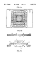
- FIGS. 3 and 4 respectively show the plan view and the sectional view of the lead frame of the prior art.
- the inner lead part 2 to which wire bonding is to be applied is coated with silver plating 5 and the outer lead part 1 is provided with a surface treatment layer containing lead and tin.
- alloys of tin incorporated with silver have attracted attention as the most promising candidate for lead-free solder, and the plating liquor for such an alloy is being developed.
- the alloy has not yet been used in practice owing to such problems as unsatisfactory appearance, development of cracks caused by bending, discoloration caused by thermal hysteresis and deterioration of solder wettability caused by thermal hysteresis.
- the objects of the present invention are to provide a lead frame for electronic parts which does not contain lead, one of the environmentally harmful pollutants, has good characteristic properties including solder wettability and bonding strength and is of low cost, to provide a semiconductor device which uses said lead frame for electronic parts, and to provide a process for producing said lead frame for electronic parts and said semiconductor device.
- the semiconductor device having tin-based solder film which does not contain lead uses a lead frame formed essentially of at least one metal selected from the group consisting of nickel and nickel alloys, copper and copper alloys, and iron and iron alloys wherein an inner lead part of the lead frame is provided with a surface treatment layer of silver or an alloy containing silver and an outer lead part of the lead frame is provided at least with a surface treatment layer of an alloy containing silver and tin of the body-centered cubic structure preferentially oriented in a (101) plane and/or a (211) plane (said surface treatment layer being hereinafter sometimes referred to as the Sn--Ag surface treatment layer).
- the above-mentioned specific crystal structure of tin can be obtained by regulating the current density at the time of plating.
- the plating liquor for forming the Sn--Ag surface treatment layer contains as an acid at least one member selected from the group consisting of alkanesulfonic acids, alkanolsulfonic acids and sulfamic acids, as a tin salt at least one member selected from the group consisting of tin alkanesulfonates and SnO, and as a silver salt at least one member selected from the group consisting of silver alkanesulfonates, Ag 2 O and AgO.
- the acid is preferably methanesulfonic acid, hydroxypropanesulfonic acid or isopropanolsulfonic acid.
- the tin alkanesulfonate is preferably tin methanesulfonate.
- the silver alkanesulfonate is preferably silver methanesulfonate.
- the plating liquor may additionally contain as a stabilizer for silver at least one member selected from the group consisting of sulfur compounds, thioamide compounds and thiol compounds, as a stabilizer for tin at least one member selected from the group consisting of carboxylic acids, sulfamic acids, pyrophosphoric acid salts, phenol compounds and chelating agents, and as a crystallization regulator at least one member selected from the group consisting of aromatic sulfonic acid salts, aliphatic sulfonic acid salts, hydantoin compounds, cysteine compounds, aromatic organic amines, aliphatic aldehydes, aromatic aldehydes, nonionic surfactants, amphoteric surfactants and anionic surfactants.
- a stabilizer for silver at least one member selected from the group consisting of sulfur compounds, thioamide compounds and thiol compounds
- tin at least one member selected from the group consisting of carboxylic acids, sulfamic acids, pyr
- the outer lead part may be treated with at least one treating agent selected from hydrochloric acid, nitric acid and sulfuric acid in advance to the formation of the Sn--Ag surface treatment layer.
- the Sn--Ag surface treatment layer may be treated with a treating agent containing sodium triphosphate.
- the thickness of the Sn--Ag surface treatment layer is preferably selected from the range of 3-15 ⁇ m.
- the silver content of the Sn--Ag surface treatment layer is selected from the range of 1-8% by weight, whereby the disadvantages of the prior lead frames can be overcome in whole, and there can be provided a lead frame for electronic parts which does not contain lead, one of the environmentally harmful pollutants, has good characteristic properties including solder wettability and bonding strength and is of low cost and a process for producing the lead frame.
- FIG. 1 is a plan view of a lead frame of one embodiment of the present invention.
- FIG. 2 is a sectional view of a lead frame of one embodiment of the present invention.
- FIG. 3 is a plan view of a lead frame of the prior art.
- FIG. 4 is a sectional view of a lead frame of the prior art.
- FIGS. 5A-5C is a sectional views of an IC package which uses the lead frame of the present invention.
- the plating which does not exert adverse influence on environment used in the present invention employs an alloy of silver and tin of the body-centered cubic structure preferentially oriented in the (101) plane and/or the (211) plane.
- coating films containing tin of the body-centered cubic structure preferentially oriented in the (220) plane can be formed, if desired.
- the plating film tends to develop cracks when the outer lead is processed by bending, and the plating film surface is apt to be oxidized due to the heat applied at the time of IC assembling, resulting in discoloration and lowered solder wettability.
- tin-silver films containing tin of the body-centered cubic structure preferentially oriented in the (101) plane and/or the (211) plane formed by controlling the crystal orientation prevent the development of cracks and undergo no discoloration and show good solder wettability even after subjected to heating.
- the tin-silver alloy involves no such problems as limited supply and high cost unlike palladium and shows characteristic properties comparable to those of tin-bismuth, tin-zinc or tin-indium. Though the tin-silver alloy has a higher melting eutectic point of 221° C.
- the alloy does not need to melt completely to wet when used as plating for the outer lead of a lead frame; it suffices if the alloy reacts with the soldering paste or solder for reflow at their interface at the time of surface packaging and produces a sufficient bonding strength. In fact, the alloy gives a bonding strength and solder wettability comparable to those obtainable by previous lead-containing solder.
- FIGS. 1 and 2 are respectively the plan view and the sectional view of the lead frame of the present invention.
- the inner lead part 2 to which wire bonding is to be applied is provided with a surface treatment layer 5 of silver or an alloy containing silver and the outer lead part 1 is provided with a Sn--Ag surface treatment layer 6 which contains silver and tin of the body-centered cubic structure preferentially oriented in the (101) plane and/or the (211) plane.
- the surface treatment layer 5 of silver or an alloy containing silver and the Sn--Ag surface treatment layer 6 may either be separated from, or be in contact with each other.
- the surface treatment layer 5 of silver or an alloy containing silver may be formed on the inner lead part 2 alone, or it may partly cover the pad 3, or it may cover the whole of the pad 3.
- the surface treatment layer 5 of silver or an alloy containing silver and the Sn--Ag surface treatment layer 6 are formed by means of plating in the present embodiment, they can also be formed by such means as physical vapor deposition, sputtering and CVD.
- physical vapor deposition preferably a direct voltage or an alternating voltage of 50 to 200 V is applied by an ion-plating method.
- sputtering preferably a bias voltage of 50 to 200 V is applied.
- a membrane is formed by Sn ions or inert gas ions incident on the surface of the substrate which have an energy of 50 to 200 V.
- the substrate used for semiconductor lead frames is made by using copper or a copper alloy such as low tin phosphorus bronze and alloy 194, or an iron-nickel alloy called 42 material obtained by adding about 42% by weight of nickel to iron.
- Fabrication of the substrate into the form of lead frame may be conducted either by a method which comprises coating photosensitive resist on the surface, printing a pattern thereon, followed by developing to leave the photosensitive resist as a positive pattern of the lead frame, and then processing the substrate with an etching solution of ferric chloride, cupric chloride, or the like, or by a method which comprises making a die for punching out the form of the desired lead frame and then subjecting the substrate to a punching operation with a pressing machine by using the die.
- Both the etching method and the punching method may be adopted as desired in the present invention.
- the substrate After having been worked into the form of a lead frame, the substrate is subjected to a washing treatment and then, if necessary, to a heat treatment step to remove the stress which has remained in the substrate after the punching operation with a press. Thereafter it is subjected to a plating step.
- the plating step of the present invention is described in detail below.
- the washing step oily substances which have sticked to the base material in the pressing step and heat treatment step are removed with an alkaline degreasing agent or the like by the dipping method or the electrical method, used each singly or in combination; thereafter, a copper underlayer plating is formed in a thickness of 0.2 ⁇ m or more.
- the copper underlayer plating liquor used may be, for example, a copper cyanide solution.
- the inner lead part 2 is plated with silver through a silver partial plating step.
- the silver plating liquor used may be, for example, a silver cyanide solution.
- the outer lead part 1 is pretreated with a treating agent selected from at least one of the hydrochloric acid, nitric acid and sulfuric acid to improve the adhesion between the base material and the Sn--Ag surface treatment layer.
- a treating agent selected from at least one of the hydrochloric acid, nitric acid and sulfuric acid to improve the adhesion between the base material and the Sn--Ag surface treatment layer.
- the base material surface is etched by the pretreatment, and the adhesion of the surface to the Sn--Ag surface treatment layer is resultantly improved through an anchoring effect.
- a Sn--Ag surface treatment layer is provided to the outer lead part 1 by partial plating.
- the plating liquor used for forming the Sn--Ag surface treatment layer contains as an acid at least one member selected from the group consisting of alkanesulfonic acids, alkanosulfonic acids and sulfamic acids, as a tin salt at least one member selected from the group consisting of tin alkane-sulfonates and SnO, and as a silver salt at least one member selected from the group consisting of silver alkanesulfonates, Ag 2 O and AgO.
- the acid is preferably methanesulfonic acid, hydroxypropanesulfonic acid or isopropanolsulfonic acid.
- the tin alkanesulfonate is preferably tin methanesulfonate.
- the silver alkane-sulfonate is preferably silver methanesulfonate.
- the plating liquor preferably contains 50-200 g/l of an acid, 20-60 g/l of tin in terms of metallic tin amount and 0.5-3 g/l of silver in terms of metallic silver amount.
- the plating liquor may contain at least one additive which includes as a stabilizer for silver at least one member selected from the group consisting of sulfur compounds, thioamide compounds, thiol compounds and thiosulfuric acid salts, as a stabilizer for tin at least one member selected from the group consisting of carboxylic acids, sulfamic acids, pyrophosphoric acid salts, phenol compounds and chelating agents, as a crystallization regulator at least one member selected from the group consisting of aromatic sulfonic acid salts, aliphatic sulfonic acid salts, hydantoin compounds, cysteine compounds, aromatic organic amines, aliphatic aldehydes, aromatic aldehydes, nonionic surfactants, amphoteric surfactants and anionic surfactants.
- the preferred amount of the additives to be added may be appropriately determined according to intended objects.
- the plating may be conducted, for example, by the jet plating method using a sparger.
- the temperature of the liquor is preferably 15 ⁇ 35° C., more preferably 25° C.
- Plating film of good quality can be obtained at current densities in the range of 15-25 A/dm 2 . Current densities over the above-mentioned range causes the increase of (220) plane orientation and resultant deterioration of film quality.
- the anode electrode can be selected as desired from insoluble electrodes which comprise at least one member selected from the group consisting of metals and oxides of platinum, iridium, tantalum, rhodium, and ruthenium. If a soluble electrode which uses a solder alloy is employed, the electrode needs to be changed frequently and the production line must be stopped each time, so that the production efficiency becomes very low.
- the plating thickness may be selected as desired from the range of 3-15 ⁇ m.
- the plating thickness is smaller than 3 ⁇ m, the solder wettability tends to be poor owing to the influence of the base material.
- the thickness is larger than 15 ⁇ m problems tend to arise such that the molding resin tends to leak through the gap of the die at the sealing step by the resin.
- the silver content may be selected as desired in the range of 1-8% by weight. When the silver content is lower than 1% by weight, whiskers of tin tend to develop. When the content is higher than 8% by weight electromigration of silver tends to occur at the time of IC operation.
- the exposed part of the initially formed copper underlayer plating onto which the silver plating and Sn--Ag plating have not been applied is removed. Further, to remove the silver which has leaked to the side of the lead, the silver which has leaked onto the frame surface is removed electrically. Thereafter the Sn--Ag treatment layer 6 of the outer lead part 1 is subjected to an etching treatment using a treating agent containing sodium triphosphate or the like to improve solder wettability. Finally the lead frame is immersed in a discoloration preventing agent and then washed with water and dried to obtain a finished product.
- FIGS. 5A-C An IC chip 7 is dry-fixed to the lead frame according to the present invention shown in FIGS. 1 and 2, and then the lead frame and the IC chip 7 are electrically connected by wire bonding. Then the IC chip 7 is sealed with molding resin 9. While, in the prior art, after the sealing, the oxide layer on the surface of the lead frame is removed and then outer solder plating is applied to the outer lead part 1, the use of the lead frame of the present invention greatly simplifies the production steps.
- An IC chip 7 is dry-fixed to a lead frame onto which Ag plating alone has been applied, and then the lead frame and the IC chip 7 are electrically connected by wire bonding. Then the IC chip 7 is sealed with molding resin 9. After the sealing, the oxide layer of the surface of the lead frame is removed, and outer solder plating of the Sn--Ag surface treatment layer is applied to the outer lead part 1 in the same manner as described in the embodiment 1. Thereafter, the Sn--Ag treatment layer 6 of the outer lead part 1 is treated with a treating agent containing sodium triphosphate to improve solder wettability, and then washed with water and dried to obtain a finished product.
- a 42 material alloy sheet was worked into the form of a lead frame and then subjected to a washing treatment and then, if necessary, to a heat treatment step to remove the stress which had remained in the substrate after the punching operation with a press.
- the lead frame was treated with a treating agent containing hydrochloric acid at 30° C. for 15 seconds to remove the impurities on the surface and to etch the surface at the same time.
- a plating liquor containing SnO, Ag 2 O and 150 g/l of methanesulfonic acid was used.
- the concentration of SnO was 40 g/l in terms of metallic tin and that of Ag 2 O was 2 g/l in terms of metallic silver.
- the above-mentioned plating liquor additionally contained 5 g/l of 2-aminobenzene thiol, 5 g/l of naphthalenesulfonic acid monopolyethylene glycol ether and 80 g/l of bisphenol A dipolyethylene glycol ether.
- the plating method used was the jet plating method using a sparger, the flow rate of the plating liquor was 400 l/min and the temperature of the liquor was 25° C.
- the anode electrode used was an insoluble electrode comprising a titanium base material and a mixture of iridium oxide and tantalum oxide coated thereon.
- the plating thickness was 8 ⁇ m and the silver content of the plating was 2% by weight.
- the exposed part of the initially formed copper underlayer plating onto which the silver plating and Sn--Ag plating had not been applied was removed and further, to remove the silver which had leaked to the side of the lead, the silver which had leaked onto the frame surface was removed electrically.
- the Sn--Ag treatment layer of the outer lead part was subjected to an etching treatment by dipping it in a treating agent containing 120 g/l of sodium triphosphate at a liquid temperature of 60° C. for 30 seconds to improve solder wettability.
- the lead frame was immersed in a discoloration preventing agent, and then washed with water and dried to obtain a finished product.
- the plating obtained was a tin-silver plating layer containing tin of the body-centered cubic structure preferentially oriented in the (101) plane and the (211) plane.
- the solder wettability was evaluated by using a solder wettability tester (Solder Checker, SWET 100, mfd. by TARUTIN Co., Ltd.) with a tin-lead (H63S) solder at a bath temperature of 230° C.
- the flux used was R-100-40 (non-halogen type).
- the outer lead part 1 was bent at an angle of 90° to observe the state of peeling of the plating film. Resultantly, the initial zero-cross time, the zero-cross time after heating at 175° C. for 24 hours and the appearance were all good as shown in Table 1.
- An alloy 194 sheet was worked into the form of a lead frame and then subjected to a washing treatment and then if necessary, to a heat treatment step to remove the stress which had remained in the substrate after the punching operation with a press.
- Example 1 the substrate was subjected to a washing step, copper underlayer plating step and silver partial plating step in the same manner as in Example 1.
- a pretreatment was carried out with a treating agent containing 50 g/l of sulfuric acid at 30° C. for 15 seconds. After the pretreatment, partial plating of Sn--Ag was applied to the outer lead part 1 at a current density of 24 ASD (A/dm 2 ).
- the plating liquor used in the present Example contained 40 g/l, in terms of metallic tin of SnO, 2 g/l, in terms of metallic silver, of AgO, and 150 g/l of methanesulfonic acid and additionally contained as additives 5 g/l of 4,4-aminodiphenyl sulfide, 5 g/l of naphthalenesulfonic acid mono-polyethylene glycol ether and 80 g/l of bisphenol A dipolyethylene glycol ether.
- the plating was conducted by jet plating using a sparger at a flow rate of plating liquor of 400 l/min and at a plating liquor temperature of 25° C.
- the anode electrode used was an insoluble electrode comprising a titanium base material and a mixture of iridium oxide and tantalum oxide coated thereon.
- the Sn--Ag plating had a thickness of 8 ⁇ m and a silver content of 2.5%. Then, the exposed part of the initially formed copper underlayer plating onto which the silver plating and Sn--Ag plating had not been applied was removed and further, to remove the silver which had leaked to the side of the lead, the silver which had leaked onto the frame surface was removed electrically. Thereafter the Sn--Ag treatment layer of the outer lead part was subjected to an etching treatment by dipping it in a treating agent containing 120 g/l of sodium triphosphate at a liquid temperature of 60° C. for 30 seconds to improve solder wettability. Finally the lead frame was immersed in a discoloration preventing agent, and then washed with water and dried to obtain a finished product.
- the plating obtained was a tin-silver plating layer containing tin of the body-centered cubic structure preferentially oriented in the (101) plane and the (211) plane.
- the solder wettability was evaluated under the same conditions as in Example 1.
- the outer lead part 1 was subjected to a bending test to observe the state of peeling. Resultantly, the initial zero-cross time, the zero-cross time after heating at 175° C. for 24 hours and the appearance were all good as shown in Table 1.
- a 42-material alloy sheet was worked into the form of a lead frame and then subjected to a washing treatment step and then, if necessary, to a heat treatment step to remove the stress which had remained in the substrate after the punching operation with a press. Then the substrate was subjected to a washing step, copper underlayer plating step and silver partial plating step in the same manner as in Example 1. After the partial plating of silver had been conducted, the outer lead part 1 was subjected, without a pretreatment, to partial plating of Sn--Ag at a current density of 60 ASD (A/dm 2 ).
- the plating liquor used in the present comparative example contained SnO, AgO and methanesulfonic acid as the base materials.
- the anode electrode used was an insoluble electrode comprising a titanium base material and a mixture of iridium oxide and tantalum oxide coated thereon.
- the Sn--Ag plating of the present comparative example had a thickness of 8 ⁇ m and a silver content of 2.5%. Then, the exposed part of the initially formed copper underlayer plating onto which the Ag plating and Sn--Ag plating had not been applied was removed and further, to remove the silver which had leaked to the side of the lead, the silver which had leaked onto the frame surface was removed electrically.
- the Sn--Ag treatment layer 6 of the outer lead part 1 was subjected to an etching treatment with a treating agent containing sodium triphosphate to improve solder wettability.
- the lead frame was immersed in a discoloration preventing agent, and then washed with water and dried to obtain a finished product.
- the plating obtained was a tin-silver layer containing tin of the body-centered cubic structure preferentially oriented in the (220) plane.
- the solder wettability was evaluated under the same conditions as in Example 1.
- the outer lead part 1 was subjected to a bending test to observe the state of peeling. Resultantly, the initial zero-cross time, the zero-cross time after heating at 175° C. for 24 hours and the appearance were all good as shown in Table 1, but cracks developed in the bending test.
- An alloy-194 sheet was worked into the form of a lead frame and then subjected to a washing step and then, if necessary, to a heat treatment step to remove the stress which had remained in the substrate after the punching operation with a press. Then the substrate was subjected to a washing step, copper underlayer plating step and silver partial plating step in the same manner as in Example 1. After the partial plating of silver had been conducted, a pretreatment using a treating agent containing nitric acid was carried out. Thereafter the outer lead part was subjected to partial plating of Sn--Ag.
- the plating liquor used in the present comparative example contained SnO, AgO and methanesulfonic acid as the base materials.
- the anode electrode used was an insoluble electrode comprising a titanium base material and a mixture of iridium oxide and tantalum oxide coated thereon.
- a Sn--Ag plating of 8 ⁇ m thickness was formed at a current density of 60 ASD (A/dm 2 ).
- the Sn--Ag plating had a silver content of 2.5%. Then, the exposed part of the initially formed copper underlayer plating onto which the Ag plating and Sn--Ag plating had not been applied was removed and further, to remove the silver which had leaked to the side of the lead, the silver which had leaked onto the frame surface was removed electrically.
- the Sn--Ag treatment layer 6 of the outer lead part 1 was treated with a treating agent containing sodium triphosphate to improve solder wettability and then, without an etching treatment, the lead frame was immersed in a discoloration preventing agent, and then washed with water and dried to obtain a finished product.
- the plating obtained was a tin-silver layer containing tin of the body-centered cubic structure preferentially oriented in the (220) plane.
- the solder wettability was evaluated under the same conditions as in Example 1.
- the outer lead part 1 was subjected to a bending test to observe the state of peeling. Resultantly, the initial zero-cross time, the zero-cross time after heating at 175° C. for 24 hours and the appearance were all inferior to those observed in Examples 1 and 2. Cracks developed in the bending test.
- FIGS. 5A-5C This Example is described with reference to FIGS. 5A-5C.
- a lead frame according to the present invention shown in FIGS. 1 and 2 was coated a die attach resin, an IC chip 7 was fixed to the frame and fixed fast by drying in an oven at 200° C. for 2 hours, and then the lead frame and the IC chip 7 were electrically connected by wire bonding. Then the IC chip 7 was sealed with molding resin 9. While, in the prior art, after the sealing, the oxide layer on the surface of the lead frame was removed and then outer solder plating was applied to the outer lead part 1, the use of the lead frame of the present invention simplified the production steps.
- a die attach resin was coated onto a lead frame to which Ag plating alone had been applied, then an IC chip 7 was fixed to the frame and fixed fast by drying in an oven at 200° C. for 2 hours, and then the lead frame and the IC chip 7 were electrically connected by wire bonding. Then the IC chip 7 was sealed with molding resin 9. After the sealing, the oxide layer on the surface of the lead frame was removed, and then an outer solder plating 8 ⁇ m in thickness was applied to the outer lead part 1 at a current density of 24 ASD (A/dm 2 ).
- the plating liquor used contained SnO, AgO and methane-sulfonic acid as the base materials.
- the surface treatment layer 6 containing silver and tin of the outer lead part 1 was treated with a treating agent containing sodium triphosphate to improve solder wettability.
- the resultant device was washed with water and dried to obtain a finished product.
- the tin in the plating layer obtained was of the body-centered cubic structure preferentially oriented in the (101) plane and the (211) plane.
Abstract
Description
              TABLE 1
______________________________________
                         Comparative
                                   Comparative
        Example 1
               Example 2 Example 1 Example 2
______________________________________
Initial zero-cross
           0.5 sec 0.45 sec   0.6 sec
                                     1.2 sec
After-heating
          0.65 sec 0.57 sec  0.79 sec
                                       5 sec
zero-cross
Bending crack
          None     None      Yes     Yes
Discoloration
          None     None      None    Yes
______________________________________
Claims (6)
Applications Claiming Priority (4)
| Application Number | Priority Date | Filing Date | Title |
|---|---|---|---|
| JP11655098A JPH11307710A (en) | 1998-04-27 | 1998-04-27 | Plated lead frame and manufacture thereof, and semiconductor device using the plated lead frame |
| JP10-116550 | 1998-04-27 | ||
| JP33541698A JP3402228B2 (en) | 1998-11-26 | 1998-11-26 | Semiconductor device having lead-free tin-based solder coating |
| JP10-335416 | 1998-11-26 |
Publications (1)
| Publication Number | Publication Date |
|---|---|
| US6087714A true US6087714A (en) | 2000-07-11 |
Family
ID=26454858
Family Applications (1)
| Application Number | Title | Priority Date | Filing Date |
|---|---|---|---|
| US09/298,841 Expired - Lifetime US6087714A (en) | 1998-04-27 | 1999-04-26 | Semiconductor devices having tin-based solder film containing no lead and process for producing the devices |
Country Status (1)
| Country | Link |
|---|---|
| US (1) | US6087714A (en) |
Cited By (29)
| Publication number | Priority date | Publication date | Assignee | Title |
|---|---|---|---|---|
| US20010015481A1 (en) * | 2000-02-18 | 2001-08-23 | Yoshinori Miyaki | Semiconductor integrated circuit device and method of manufacturing the same |
| US6376901B1 (en) * | 1999-06-08 | 2002-04-23 | Texas Instruments Incorporated | Palladium-spot leadframes for solder plated semiconductor devices and method of fabrication |
| US6395583B1 (en) * | 1999-04-22 | 2002-05-28 | Matsushita Electric Industrial Co., Ltd. | Semiconductor device with a coating of Pb-free Sn-base solder and manufacturing method therefor |
| US20020146864A1 (en) * | 2001-04-04 | 2002-10-10 | Yoshinori Miyaki | Semiconductor device and method of manufacturing the same |
| US6469386B1 (en) * | 1999-10-01 | 2002-10-22 | Samsung Aerospace Industries, Ltd. | Lead frame and method for plating the same |
| US6545344B2 (en) * | 2000-06-27 | 2003-04-08 | Texas Instruments Incorporated | Semiconductor leadframes plated with lead-free solder and minimum palladium |
| US20030082398A1 (en) * | 2001-10-24 | 2003-05-01 | Hisahiro Tanaka | Method for producing tin-silver alloy plating film, the tin-silver alloy plating film and lead frame for electronic parts having the plating film |
| DE10158227A1 (en) * | 2001-11-15 | 2003-06-05 | Siemens Ag | Electrolysis bath for the electrodeposition of silver-tin alloys |
| US6575354B2 (en) * | 2000-11-20 | 2003-06-10 | Matsushita Electric Industrial Co., Ltd. | Method for producing tin-silver alloy plating film, the tin-silver alloy plating film and lead frame for electronic parts having the film |
| US6583500B1 (en) * | 2002-02-11 | 2003-06-24 | Texas Instruments Incorporated | Thin tin preplated semiconductor leadframes |
| US6646330B2 (en) * | 2000-09-21 | 2003-11-11 | Matsushita Electric Industrial Co., Ltd. | Lead frame for semiconductor device, process for producing the same and semiconductor device using the same |
| US20040256239A1 (en) * | 2003-05-12 | 2004-12-23 | Rohm And Haas Electronic Materials, L.L.C. | Tin plating method |
| US20060022313A1 (en) * | 2004-07-29 | 2006-02-02 | Peng Su | Solderable metal finish for integrated circuit package leads and method for forming |
| US20060189037A1 (en) * | 2005-02-18 | 2006-08-24 | Texas Instruments Incorporated | Low cost method to produce high volume lead frames |
| US20060231931A1 (en) * | 2005-04-15 | 2006-10-19 | Samsung Techwin Co., Ltd. | Lead frame for semiconductor package |
| US20070182006A1 (en) * | 2006-02-03 | 2007-08-09 | Masazumi Amagai | Semiconductor device with an improved solder joint |
| US20080001264A1 (en) * | 2006-07-03 | 2008-01-03 | Texas Instruments Incorporated | Exposed top side copper leadframe manufacturing |
| US20090108420A1 (en) * | 2007-10-26 | 2009-04-30 | Yasutaka Okura | Semiconductor device and its fabrication process |
| US20100230700A1 (en) * | 2009-03-10 | 2010-09-16 | Ki Bum Kim | Light emitting device package |
| US20110268920A1 (en) * | 2005-03-24 | 2011-11-03 | Dowa Metaltech Co., Ltd. | Tin-plated product and method for producing same |
| US20130316496A1 (en) * | 2012-05-24 | 2013-11-28 | Sts Semiconductor & Telecommunications Co., Ltd. | Method of manufacturing semiconductor package having no chip pad |
| US20150228561A1 (en) * | 2014-02-07 | 2015-08-13 | Dawning Leading Technology Inc | Lead frame structure for quad flat no-lead package, quad flat no-lead package and method for forming the lead frame structure |
| US20170040183A1 (en) * | 2015-08-07 | 2017-02-09 | Shinko Electric Industries Co., Ltd. | Lead frame and semiconductor device |
| US20170263695A1 (en) * | 2016-03-11 | 2017-09-14 | International Business Machines Corporation | Deformable and flexible capacitor |
| US10763196B1 (en) * | 2019-03-22 | 2020-09-01 | Ohkuchi Materials Co., Ltd. | Lead frame |
| US10763204B2 (en) * | 2016-09-12 | 2020-09-01 | Denso Corporation | Semiconductor device |
| US10903150B2 (en) * | 2019-03-22 | 2021-01-26 | Ohkuchi Materials Co., Ltd. | Lead frame |
| US11404286B2 (en) * | 2019-03-22 | 2022-08-02 | Ohkuchi Materials Co., Ltd. | Lead frame |
| TWI826671B (en) * | 2019-03-28 | 2023-12-21 | 長華科技股份有限公司 | Semiconductor element mounting parts, lead frames, and semiconductor element mounting substrates |
Citations (6)
| Publication number | Priority date | Publication date | Assignee | Title |
|---|---|---|---|---|
| US4707724A (en) * | 1984-06-04 | 1987-11-17 | Hitachi, Ltd. | Semiconductor device and method of manufacturing thereof |
| JPS62287657A (en) * | 1986-06-06 | 1987-12-14 | Mitsubishi Electric Corp | Semiconductor device |
| US5167794A (en) * | 1990-04-16 | 1992-12-01 | Mitsubishi Denki Kabushiki Kaisha | Method for producing lead frame material |
| US5221859A (en) * | 1990-02-26 | 1993-06-22 | Hitachi, Ltd. | Lead frame for semiconductor device |
| US5521432A (en) * | 1991-10-14 | 1996-05-28 | Fujitsu Limited | Semiconductor device having improved leads comprising palladium plated nickel |
| JPH10102283A (en) * | 1996-09-26 | 1998-04-21 | Daiwa Kasei Kenkyusho:Kk | Electric electronic circuit parts |
-
1999
- 1999-04-26 US US09/298,841 patent/US6087714A/en not_active Expired - Lifetime
Patent Citations (6)
| Publication number | Priority date | Publication date | Assignee | Title |
|---|---|---|---|---|
| US4707724A (en) * | 1984-06-04 | 1987-11-17 | Hitachi, Ltd. | Semiconductor device and method of manufacturing thereof |
| JPS62287657A (en) * | 1986-06-06 | 1987-12-14 | Mitsubishi Electric Corp | Semiconductor device |
| US5221859A (en) * | 1990-02-26 | 1993-06-22 | Hitachi, Ltd. | Lead frame for semiconductor device |
| US5167794A (en) * | 1990-04-16 | 1992-12-01 | Mitsubishi Denki Kabushiki Kaisha | Method for producing lead frame material |
| US5521432A (en) * | 1991-10-14 | 1996-05-28 | Fujitsu Limited | Semiconductor device having improved leads comprising palladium plated nickel |
| JPH10102283A (en) * | 1996-09-26 | 1998-04-21 | Daiwa Kasei Kenkyusho:Kk | Electric electronic circuit parts |
Cited By (65)
| Publication number | Priority date | Publication date | Assignee | Title |
|---|---|---|---|---|
| US6395583B1 (en) * | 1999-04-22 | 2002-05-28 | Matsushita Electric Industrial Co., Ltd. | Semiconductor device with a coating of Pb-free Sn-base solder and manufacturing method therefor |
| US6376901B1 (en) * | 1999-06-08 | 2002-04-23 | Texas Instruments Incorporated | Palladium-spot leadframes for solder plated semiconductor devices and method of fabrication |
| US6469386B1 (en) * | 1999-10-01 | 2002-10-22 | Samsung Aerospace Industries, Ltd. | Lead frame and method for plating the same |
| CN100380650C (en) * | 2000-02-18 | 2008-04-09 | 株式会社日立制作所 | Semiconductor integrated circuit device and mfg. method thereof |
| US20090014855A1 (en) * | 2000-02-18 | 2009-01-15 | Yoshinori Miyaki | Semiconductor integrated circuit device and method of manufacturing the same |
| EP1126520A3 (en) * | 2000-02-18 | 2002-11-20 | Hitachi, Ltd. | IC device and method of manufacturing the same |
| US7397114B2 (en) | 2000-02-18 | 2008-07-08 | Renesas Technology Corp. | Semiconductor integrated circuit device and method of manufacturing the same |
| US6891253B2 (en) * | 2000-02-18 | 2005-05-10 | Renesas Technology Corp. | Semiconductor integrated circuit device and method of manufacturing the same |
| US20010015481A1 (en) * | 2000-02-18 | 2001-08-23 | Yoshinori Miyaki | Semiconductor integrated circuit device and method of manufacturing the same |
| US7176056B2 (en) | 2000-02-18 | 2007-02-13 | Renesas Technology Corp. | Semiconductor integrated circuit device and method of manufacturing the same |
| US20040245607A1 (en) * | 2000-02-18 | 2004-12-09 | Yoshinori Miyaki | Semiconductor integrated circuit device and method of manufacturing the same |
| US20060138617A1 (en) * | 2000-02-18 | 2006-06-29 | Yoshinori Miyaki | Semiconductor integrated circuit device and method of manufacturing the same |
| US7038306B2 (en) | 2000-02-18 | 2006-05-02 | Hitachi, Ltd. | Semiconductor integrated circuit device and method of manufacturing the same |
| US6545344B2 (en) * | 2000-06-27 | 2003-04-08 | Texas Instruments Incorporated | Semiconductor leadframes plated with lead-free solder and minimum palladium |
| US6646330B2 (en) * | 2000-09-21 | 2003-11-11 | Matsushita Electric Industrial Co., Ltd. | Lead frame for semiconductor device, process for producing the same and semiconductor device using the same |
| US6575354B2 (en) * | 2000-11-20 | 2003-06-10 | Matsushita Electric Industrial Co., Ltd. | Method for producing tin-silver alloy plating film, the tin-silver alloy plating film and lead frame for electronic parts having the film |
| US6960823B2 (en) * | 2001-04-04 | 2005-11-01 | Renesas Technology Corp. | Semiconductor device and method of manufacturing the same |
| US20050196903A1 (en) * | 2001-04-04 | 2005-09-08 | Yoshinori Miyaki | Semiconductor device and method of manufacturing the same |
| US7528014B2 (en) | 2001-04-04 | 2009-05-05 | Renesas Technology Corp. | Semiconductor device and method of manufacturing the same |
| US20050258524A1 (en) * | 2001-04-04 | 2005-11-24 | Yoshinori Miyaki | Semiconductor device and method of manufacturing the same |
| US7541667B2 (en) | 2001-04-04 | 2009-06-02 | Hitachi, Ltd. | Semiconductor device and method of manufacturing the same |
| US20020146864A1 (en) * | 2001-04-04 | 2002-10-10 | Yoshinori Miyaki | Semiconductor device and method of manufacturing the same |
| US20030082398A1 (en) * | 2001-10-24 | 2003-05-01 | Hisahiro Tanaka | Method for producing tin-silver alloy plating film, the tin-silver alloy plating film and lead frame for electronic parts having the plating film |
| US6677056B2 (en) * | 2001-10-24 | 2004-01-13 | Matsushita Electric Industrial Co., Ltd. | Method for producing tin-silver alloy plating film, the tin-silver alloy plating film and lead frame for electronic parts having the plating film |
| US20050077186A1 (en) * | 2001-11-15 | 2005-04-14 | Christian Hansen | Electrolysis bath for electrodepositing silver-tin alloys |
| DE10158227A1 (en) * | 2001-11-15 | 2003-06-05 | Siemens Ag | Electrolysis bath for the electrodeposition of silver-tin alloys |
| US6583500B1 (en) * | 2002-02-11 | 2003-06-24 | Texas Instruments Incorporated | Thin tin preplated semiconductor leadframes |
| US7695605B2 (en) * | 2003-05-12 | 2010-04-13 | Rohm And Haas Electronic Materials Llc | Tin plating method |
| US20040256239A1 (en) * | 2003-05-12 | 2004-12-23 | Rohm And Haas Electronic Materials, L.L.C. | Tin plating method |
| US7215014B2 (en) * | 2004-07-29 | 2007-05-08 | Freescale Semiconductor, Inc. | Solderable metal finish for integrated circuit package leads and method for forming |
| US20060022313A1 (en) * | 2004-07-29 | 2006-02-02 | Peng Su | Solderable metal finish for integrated circuit package leads and method for forming |
| US20070164405A1 (en) * | 2005-02-18 | 2007-07-19 | Texas Instruments Incorporated | Low Cost Method to Produce High Volume Lead Frames |
| US7192809B2 (en) * | 2005-02-18 | 2007-03-20 | Texas Instruments Incorporated | Low cost method to produce high volume lead frames |
| WO2006089296A3 (en) * | 2005-02-18 | 2007-03-15 | Texas Instruments Inc | Low cost, high volume lead frame production |
| US7368807B2 (en) | 2005-02-18 | 2008-05-06 | Texas Instruments Incorporated | Low cost method to produce high volume lead frames |
| US20060189037A1 (en) * | 2005-02-18 | 2006-08-24 | Texas Instruments Incorporated | Low cost method to produce high volume lead frames |
| US20110268920A1 (en) * | 2005-03-24 | 2011-11-03 | Dowa Metaltech Co., Ltd. | Tin-plated product and method for producing same |
| US7285845B2 (en) | 2005-04-15 | 2007-10-23 | Samsung Techwin Co., Ltd. | Lead frame for semiconductor package |
| US20060231931A1 (en) * | 2005-04-15 | 2006-10-19 | Samsung Techwin Co., Ltd. | Lead frame for semiconductor package |
| WO2007092762A3 (en) * | 2006-02-03 | 2008-04-03 | Texas Instruments Inc | Semiconductor device with improved solder joint |
| US7626274B2 (en) | 2006-02-03 | 2009-12-01 | Texas Instruments Incorporated | Semiconductor device with an improved solder joint |
| US20070182006A1 (en) * | 2006-02-03 | 2007-08-09 | Masazumi Amagai | Semiconductor device with an improved solder joint |
| US20080001264A1 (en) * | 2006-07-03 | 2008-01-03 | Texas Instruments Incorporated | Exposed top side copper leadframe manufacturing |
| US20090108420A1 (en) * | 2007-10-26 | 2009-04-30 | Yasutaka Okura | Semiconductor device and its fabrication process |
| EP2053656A3 (en) * | 2007-10-26 | 2010-05-05 | Renesas Technology Corp. | Semiconductor device and its fabrication process |
| EP2385550A1 (en) * | 2007-10-26 | 2011-11-09 | Renesas Electronics Corporation | Semiconductor device and its fabrication process |
| US20100230700A1 (en) * | 2009-03-10 | 2010-09-16 | Ki Bum Kim | Light emitting device package |
| US20130316496A1 (en) * | 2012-05-24 | 2013-11-28 | Sts Semiconductor & Telecommunications Co., Ltd. | Method of manufacturing semiconductor package having no chip pad |
| US8802498B2 (en) * | 2012-05-24 | 2014-08-12 | Sts Semiconductor & Telecommunications Co., Ltd. | Method of manufacturing semiconductor package having no chip pad |
| US9607933B2 (en) * | 2014-02-07 | 2017-03-28 | Dawning Leading Technology Inc. | Lead frame structure for quad flat no-lead package, quad flat no-lead package and method for forming the lead frame structure |
| US20150228561A1 (en) * | 2014-02-07 | 2015-08-13 | Dawning Leading Technology Inc | Lead frame structure for quad flat no-lead package, quad flat no-lead package and method for forming the lead frame structure |
| US20170040183A1 (en) * | 2015-08-07 | 2017-02-09 | Shinko Electric Industries Co., Ltd. | Lead frame and semiconductor device |
| CN106449421A (en) * | 2015-08-07 | 2017-02-22 | 新光电气工业株式会社 | Lead frame, semiconductor device and method for producing lead frame |
| CN106449421B (en) * | 2015-08-07 | 2021-03-02 | 新光电气工业株式会社 | Lead frame, semiconductor device, and method for manufacturing lead frame |
| US9779966B2 (en) * | 2015-08-07 | 2017-10-03 | Shinko Electric Industries Co., Ltd. | Lead frame and semiconductor device |
| US10672865B2 (en) * | 2016-03-11 | 2020-06-02 | International Business Machines Corporation | Deformable and flexible capacitor |
| US10134831B2 (en) * | 2016-03-11 | 2018-11-20 | International Business Machines Corporation | Deformable and flexible capacitor |
| US20170263695A1 (en) * | 2016-03-11 | 2017-09-14 | International Business Machines Corporation | Deformable and flexible capacitor |
| US10763204B2 (en) * | 2016-09-12 | 2020-09-01 | Denso Corporation | Semiconductor device |
| US10763196B1 (en) * | 2019-03-22 | 2020-09-01 | Ohkuchi Materials Co., Ltd. | Lead frame |
| US20200303287A1 (en) * | 2019-03-22 | 2020-09-24 | Ohkuchi Materials Co., Ltd. | Lead frame |
| US10903150B2 (en) * | 2019-03-22 | 2021-01-26 | Ohkuchi Materials Co., Ltd. | Lead frame |
| US11404286B2 (en) * | 2019-03-22 | 2022-08-02 | Ohkuchi Materials Co., Ltd. | Lead frame |
| TWI820313B (en) * | 2019-03-22 | 2023-11-01 | 日商大口電材股份有限公司 | Lead frame |
| TWI826671B (en) * | 2019-03-28 | 2023-12-21 | 長華科技股份有限公司 | Semiconductor element mounting parts, lead frames, and semiconductor element mounting substrates |
Similar Documents
| Publication | Publication Date | Title |
|---|---|---|
| US6087714A (en) | Semiconductor devices having tin-based solder film containing no lead and process for producing the devices | |
| US6646330B2 (en) | Lead frame for semiconductor device, process for producing the same and semiconductor device using the same | |
| KR920000592B1 (en) | Tin whisker-free tin or tin alloy plated article and coating technique thereof | |
| US5320272A (en) | Tin-bismuth solder connection having improved high temperature properties, and process for forming same | |
| JP3314754B2 (en) | Semiconductor device having lead-free tin-based solder film and method of manufacturing the same | |
| US7488408B2 (en) | Tin-plated film and method for producing the same | |
| Christie et al. | Gold electrodeposition within the electronics industry | |
| US20030082398A1 (en) | Method for producing tin-silver alloy plating film, the tin-silver alloy plating film and lead frame for electronic parts having the plating film | |
| US6037653A (en) | Semiconductor lead frame having multi-layered plating layer including copper-nickel plating layer | |
| US5316205A (en) | Method for forming gold bump connection using tin-bismuth solder | |
| KR20070028266A (en) | Metal duplex and method | |
| TWI386523B (en) | Sn-b electro-plating solution and electro-plating method using it | |
| JP4639701B2 (en) | Metal plate having tin plating film, electronic component including the same, and method for producing tin plating film | |
| JP2000265294A (en) | Tin and tin alloy plating bath, plating film and lead frame for semiconductor device | |
| JP2002161396A (en) | Method for manufacturing tin - silver alloy plated film, and tin - silver alloy plated film, and lead frame for electronic component therewith | |
| JPH10284667A (en) | Material for electric electronic device component having superior corrosion resistance and oxidation resistance | |
| JP3402228B2 (en) | Semiconductor device having lead-free tin-based solder coating | |
| JPH0574778A (en) | Bump and forming method of thereof | |
| JPH11307710A (en) | Plated lead frame and manufacture thereof, and semiconductor device using the plated lead frame | |
| JP4117537B2 (en) | How to prevent tin whiskers | |
| Schetty | Lead-free finishes for printed circuit boards and components | |
| JPS6153434B2 (en) | ||
| JPH04174546A (en) | Manufacture of semiconductor lead frame | |
| Puttlitz et al. | Lead-Free Finishes for Printed Circuit Boards and Components Rob Schetty | |
| EP0136713A2 (en) | Electric contact member and method of making same |
Legal Events
| Date | Code | Title | Description |
|---|---|---|---|
| AS | Assignment |
Owner name: MATSUSHITA ELECTRIC INDUSTRIAL CO., LTD., JAPAN Free format text: ASSIGNMENT OF ASSIGNORS INTEREST;ASSIGNORS:KUBARA, TAKASHI;MASUDA, MATSUO;TOKIWA, TSUYOSHI;AND OTHERS;REEL/FRAME:009924/0021 Effective date: 19990412 |
|
| STCF | Information on status: patent grant |
Free format text: PATENTED CASE |
|
| FEPP | Fee payment procedure |
Free format text: PAYOR NUMBER ASSIGNED (ORIGINAL EVENT CODE: ASPN); ENTITY STATUS OF PATENT OWNER: LARGE ENTITY |
|
| FPAY | Fee payment |
Year of fee payment: 4 |
|
| FPAY | Fee payment |
Year of fee payment: 8 |
|
| FEPP | Fee payment procedure |
Free format text: PAYOR NUMBER ASSIGNED (ORIGINAL EVENT CODE: ASPN); ENTITY STATUS OF PATENT OWNER: LARGE ENTITY Free format text: PAYER NUMBER DE-ASSIGNED (ORIGINAL EVENT CODE: RMPN); ENTITY STATUS OF PATENT OWNER: LARGE ENTITY |
|
| FPAY | Fee payment |
Year of fee payment: 12 |