US6066890A - Separate circuit devices in an intra-package configuration and assembly techniques - Google Patents
Separate circuit devices in an intra-package configuration and assembly techniques Download PDFInfo
- Publication number
- US6066890A US6066890A US08/556,369 US55636995A US6066890A US 6066890 A US6066890 A US 6066890A US 55636995 A US55636995 A US 55636995A US 6066890 A US6066890 A US 6066890A
- Authority
- US
- United States
- Prior art keywords
- circuit
- mounting platform
- circuit device
- package configuration
- integrated circuit
- Prior art date
- Legal status (The legal status is an assumption and is not a legal conclusion. Google has not performed a legal analysis and makes no representation as to the accuracy of the status listed.)
- Expired - Lifetime
Links
Images


Classifications
-
- H—ELECTRICITY
- H01—ELECTRIC ELEMENTS
- H01L—SEMICONDUCTOR DEVICES NOT COVERED BY CLASS H10
- H01L24/00—Arrangements for connecting or disconnecting semiconductor or solid-state bodies; Methods or apparatus related thereto
- H01L24/01—Means for bonding being attached to, or being formed on, the surface to be connected, e.g. chip-to-package, die-attach, "first-level" interconnects; Manufacturing methods related thereto
- H01L24/42—Wire connectors; Manufacturing methods related thereto
- H01L24/47—Structure, shape, material or disposition of the wire connectors after the connecting process
- H01L24/48—Structure, shape, material or disposition of the wire connectors after the connecting process of an individual wire connector
-
- H—ELECTRICITY
- H01—ELECTRIC ELEMENTS
- H01L—SEMICONDUCTOR DEVICES NOT COVERED BY CLASS H10
- H01L23/00—Details of semiconductor or other solid state devices
- H01L23/48—Arrangements for conducting electric current to or from the solid state body in operation, e.g. leads, terminal arrangements ; Selection of materials therefor
- H01L23/488—Arrangements for conducting electric current to or from the solid state body in operation, e.g. leads, terminal arrangements ; Selection of materials therefor consisting of soldered or bonded constructions
- H01L23/495—Lead-frames or other flat leads
- H01L23/49541—Geometry of the lead-frame
-
- H—ELECTRICITY
- H01—ELECTRIC ELEMENTS
- H01L—SEMICONDUCTOR DEVICES NOT COVERED BY CLASS H10
- H01L23/00—Details of semiconductor or other solid state devices
- H01L23/48—Arrangements for conducting electric current to or from the solid state body in operation, e.g. leads, terminal arrangements ; Selection of materials therefor
- H01L23/488—Arrangements for conducting electric current to or from the solid state body in operation, e.g. leads, terminal arrangements ; Selection of materials therefor consisting of soldered or bonded constructions
- H01L23/495—Lead-frames or other flat leads
- H01L23/49575—Assemblies of semiconductor devices on lead frames
-
- H—ELECTRICITY
- H01—ELECTRIC ELEMENTS
- H01L—SEMICONDUCTOR DEVICES NOT COVERED BY CLASS H10
- H01L24/00—Arrangements for connecting or disconnecting semiconductor or solid-state bodies; Methods or apparatus related thereto
- H01L24/01—Means for bonding being attached to, or being formed on, the surface to be connected, e.g. chip-to-package, die-attach, "first-level" interconnects; Manufacturing methods related thereto
- H01L24/02—Bonding areas ; Manufacturing methods related thereto
- H01L24/04—Structure, shape, material or disposition of the bonding areas prior to the connecting process
- H01L24/05—Structure, shape, material or disposition of the bonding areas prior to the connecting process of an individual bonding area
-
- H—ELECTRICITY
- H01—ELECTRIC ELEMENTS
- H01L—SEMICONDUCTOR DEVICES NOT COVERED BY CLASS H10
- H01L24/00—Arrangements for connecting or disconnecting semiconductor or solid-state bodies; Methods or apparatus related thereto
- H01L24/01—Means for bonding being attached to, or being formed on, the surface to be connected, e.g. chip-to-package, die-attach, "first-level" interconnects; Manufacturing methods related thereto
- H01L24/02—Bonding areas ; Manufacturing methods related thereto
- H01L24/04—Structure, shape, material or disposition of the bonding areas prior to the connecting process
- H01L24/06—Structure, shape, material or disposition of the bonding areas prior to the connecting process of a plurality of bonding areas
-
- H—ELECTRICITY
- H01—ELECTRIC ELEMENTS
- H01L—SEMICONDUCTOR DEVICES NOT COVERED BY CLASS H10
- H01L24/00—Arrangements for connecting or disconnecting semiconductor or solid-state bodies; Methods or apparatus related thereto
- H01L24/01—Means for bonding being attached to, or being formed on, the surface to be connected, e.g. chip-to-package, die-attach, "first-level" interconnects; Manufacturing methods related thereto
- H01L24/42—Wire connectors; Manufacturing methods related thereto
- H01L24/47—Structure, shape, material or disposition of the wire connectors after the connecting process
- H01L24/49—Structure, shape, material or disposition of the wire connectors after the connecting process of a plurality of wire connectors
-
- H—ELECTRICITY
- H01—ELECTRIC ELEMENTS
- H01L—SEMICONDUCTOR DEVICES NOT COVERED BY CLASS H10
- H01L2224/00—Indexing scheme for arrangements for connecting or disconnecting semiconductor or solid-state bodies and methods related thereto as covered by H01L24/00
- H01L2224/01—Means for bonding being attached to, or being formed on, the surface to be connected, e.g. chip-to-package, die-attach, "first-level" interconnects; Manufacturing methods related thereto
- H01L2224/02—Bonding areas; Manufacturing methods related thereto
- H01L2224/04—Structure, shape, material or disposition of the bonding areas prior to the connecting process
- H01L2224/04042—Bonding areas specifically adapted for wire connectors, e.g. wirebond pads
-
- H—ELECTRICITY
- H01—ELECTRIC ELEMENTS
- H01L—SEMICONDUCTOR DEVICES NOT COVERED BY CLASS H10
- H01L2224/00—Indexing scheme for arrangements for connecting or disconnecting semiconductor or solid-state bodies and methods related thereto as covered by H01L24/00
- H01L2224/01—Means for bonding being attached to, or being formed on, the surface to be connected, e.g. chip-to-package, die-attach, "first-level" interconnects; Manufacturing methods related thereto
- H01L2224/02—Bonding areas; Manufacturing methods related thereto
- H01L2224/04—Structure, shape, material or disposition of the bonding areas prior to the connecting process
- H01L2224/05—Structure, shape, material or disposition of the bonding areas prior to the connecting process of an individual bonding area
- H01L2224/0554—External layer
- H01L2224/0555—Shape
- H01L2224/05552—Shape in top view
- H01L2224/05554—Shape in top view being square
-
- H—ELECTRICITY
- H01—ELECTRIC ELEMENTS
- H01L—SEMICONDUCTOR DEVICES NOT COVERED BY CLASS H10
- H01L2224/00—Indexing scheme for arrangements for connecting or disconnecting semiconductor or solid-state bodies and methods related thereto as covered by H01L24/00
- H01L2224/01—Means for bonding being attached to, or being formed on, the surface to be connected, e.g. chip-to-package, die-attach, "first-level" interconnects; Manufacturing methods related thereto
- H01L2224/02—Bonding areas; Manufacturing methods related thereto
- H01L2224/04—Structure, shape, material or disposition of the bonding areas prior to the connecting process
- H01L2224/05—Structure, shape, material or disposition of the bonding areas prior to the connecting process of an individual bonding area
- H01L2224/0554—External layer
- H01L2224/05599—Material
-
- H—ELECTRICITY
- H01—ELECTRIC ELEMENTS
- H01L—SEMICONDUCTOR DEVICES NOT COVERED BY CLASS H10
- H01L2224/00—Indexing scheme for arrangements for connecting or disconnecting semiconductor or solid-state bodies and methods related thereto as covered by H01L24/00
- H01L2224/01—Means for bonding being attached to, or being formed on, the surface to be connected, e.g. chip-to-package, die-attach, "first-level" interconnects; Manufacturing methods related thereto
- H01L2224/02—Bonding areas; Manufacturing methods related thereto
- H01L2224/04—Structure, shape, material or disposition of the bonding areas prior to the connecting process
- H01L2224/06—Structure, shape, material or disposition of the bonding areas prior to the connecting process of a plurality of bonding areas
- H01L2224/0601—Structure
- H01L2224/0603—Bonding areas having different sizes, e.g. different heights or widths
-
- H—ELECTRICITY
- H01—ELECTRIC ELEMENTS
- H01L—SEMICONDUCTOR DEVICES NOT COVERED BY CLASS H10
- H01L2224/00—Indexing scheme for arrangements for connecting or disconnecting semiconductor or solid-state bodies and methods related thereto as covered by H01L24/00
- H01L2224/01—Means for bonding being attached to, or being formed on, the surface to be connected, e.g. chip-to-package, die-attach, "first-level" interconnects; Manufacturing methods related thereto
- H01L2224/26—Layer connectors, e.g. plate connectors, solder or adhesive layers; Manufacturing methods related thereto
- H01L2224/31—Structure, shape, material or disposition of the layer connectors after the connecting process
- H01L2224/32—Structure, shape, material or disposition of the layer connectors after the connecting process of an individual layer connector
- H01L2224/321—Disposition
- H01L2224/32151—Disposition the layer connector connecting between a semiconductor or solid-state body and an item not being a semiconductor or solid-state body, e.g. chip-to-substrate, chip-to-passive
- H01L2224/32221—Disposition the layer connector connecting between a semiconductor or solid-state body and an item not being a semiconductor or solid-state body, e.g. chip-to-substrate, chip-to-passive the body and the item being stacked
- H01L2224/32245—Disposition the layer connector connecting between a semiconductor or solid-state body and an item not being a semiconductor or solid-state body, e.g. chip-to-substrate, chip-to-passive the body and the item being stacked the item being metallic
-
- H—ELECTRICITY
- H01—ELECTRIC ELEMENTS
- H01L—SEMICONDUCTOR DEVICES NOT COVERED BY CLASS H10
- H01L2224/00—Indexing scheme for arrangements for connecting or disconnecting semiconductor or solid-state bodies and methods related thereto as covered by H01L24/00
- H01L2224/01—Means for bonding being attached to, or being formed on, the surface to be connected, e.g. chip-to-package, die-attach, "first-level" interconnects; Manufacturing methods related thereto
- H01L2224/42—Wire connectors; Manufacturing methods related thereto
- H01L2224/47—Structure, shape, material or disposition of the wire connectors after the connecting process
- H01L2224/48—Structure, shape, material or disposition of the wire connectors after the connecting process of an individual wire connector
- H01L2224/4805—Shape
- H01L2224/4809—Loop shape
- H01L2224/48095—Kinked
-
- H—ELECTRICITY
- H01—ELECTRIC ELEMENTS
- H01L—SEMICONDUCTOR DEVICES NOT COVERED BY CLASS H10
- H01L2224/00—Indexing scheme for arrangements for connecting or disconnecting semiconductor or solid-state bodies and methods related thereto as covered by H01L24/00
- H01L2224/01—Means for bonding being attached to, or being formed on, the surface to be connected, e.g. chip-to-package, die-attach, "first-level" interconnects; Manufacturing methods related thereto
- H01L2224/42—Wire connectors; Manufacturing methods related thereto
- H01L2224/47—Structure, shape, material or disposition of the wire connectors after the connecting process
- H01L2224/48—Structure, shape, material or disposition of the wire connectors after the connecting process of an individual wire connector
- H01L2224/481—Disposition
- H01L2224/48135—Connecting between different semiconductor or solid-state bodies, i.e. chip-to-chip
- H01L2224/48137—Connecting between different semiconductor or solid-state bodies, i.e. chip-to-chip the bodies being arranged next to each other, e.g. on a common substrate
-
- H—ELECTRICITY
- H01—ELECTRIC ELEMENTS
- H01L—SEMICONDUCTOR DEVICES NOT COVERED BY CLASS H10
- H01L2224/00—Indexing scheme for arrangements for connecting or disconnecting semiconductor or solid-state bodies and methods related thereto as covered by H01L24/00
- H01L2224/01—Means for bonding being attached to, or being formed on, the surface to be connected, e.g. chip-to-package, die-attach, "first-level" interconnects; Manufacturing methods related thereto
- H01L2224/42—Wire connectors; Manufacturing methods related thereto
- H01L2224/47—Structure, shape, material or disposition of the wire connectors after the connecting process
- H01L2224/48—Structure, shape, material or disposition of the wire connectors after the connecting process of an individual wire connector
- H01L2224/481—Disposition
- H01L2224/48151—Connecting between a semiconductor or solid-state body and an item not being a semiconductor or solid-state body, e.g. chip-to-substrate, chip-to-passive
- H01L2224/48221—Connecting between a semiconductor or solid-state body and an item not being a semiconductor or solid-state body, e.g. chip-to-substrate, chip-to-passive the body and the item being stacked
- H01L2224/48245—Connecting between a semiconductor or solid-state body and an item not being a semiconductor or solid-state body, e.g. chip-to-substrate, chip-to-passive the body and the item being stacked the item being metallic
- H01L2224/48247—Connecting between a semiconductor or solid-state body and an item not being a semiconductor or solid-state body, e.g. chip-to-substrate, chip-to-passive the body and the item being stacked the item being metallic connecting the wire to a bond pad of the item
-
- H—ELECTRICITY
- H01—ELECTRIC ELEMENTS
- H01L—SEMICONDUCTOR DEVICES NOT COVERED BY CLASS H10
- H01L2224/00—Indexing scheme for arrangements for connecting or disconnecting semiconductor or solid-state bodies and methods related thereto as covered by H01L24/00
- H01L2224/01—Means for bonding being attached to, or being formed on, the surface to be connected, e.g. chip-to-package, die-attach, "first-level" interconnects; Manufacturing methods related thereto
- H01L2224/42—Wire connectors; Manufacturing methods related thereto
- H01L2224/47—Structure, shape, material or disposition of the wire connectors after the connecting process
- H01L2224/48—Structure, shape, material or disposition of the wire connectors after the connecting process of an individual wire connector
- H01L2224/481—Disposition
- H01L2224/48151—Connecting between a semiconductor or solid-state body and an item not being a semiconductor or solid-state body, e.g. chip-to-substrate, chip-to-passive
- H01L2224/48221—Connecting between a semiconductor or solid-state body and an item not being a semiconductor or solid-state body, e.g. chip-to-substrate, chip-to-passive the body and the item being stacked
- H01L2224/48245—Connecting between a semiconductor or solid-state body and an item not being a semiconductor or solid-state body, e.g. chip-to-substrate, chip-to-passive the body and the item being stacked the item being metallic
- H01L2224/48257—Connecting between a semiconductor or solid-state body and an item not being a semiconductor or solid-state body, e.g. chip-to-substrate, chip-to-passive the body and the item being stacked the item being metallic connecting the wire to a die pad of the item
-
- H—ELECTRICITY
- H01—ELECTRIC ELEMENTS
- H01L—SEMICONDUCTOR DEVICES NOT COVERED BY CLASS H10
- H01L2224/00—Indexing scheme for arrangements for connecting or disconnecting semiconductor or solid-state bodies and methods related thereto as covered by H01L24/00
- H01L2224/01—Means for bonding being attached to, or being formed on, the surface to be connected, e.g. chip-to-package, die-attach, "first-level" interconnects; Manufacturing methods related thereto
- H01L2224/42—Wire connectors; Manufacturing methods related thereto
- H01L2224/47—Structure, shape, material or disposition of the wire connectors after the connecting process
- H01L2224/48—Structure, shape, material or disposition of the wire connectors after the connecting process of an individual wire connector
- H01L2224/484—Connecting portions
- H01L2224/48463—Connecting portions the connecting portion on the bonding area of the semiconductor or solid-state body being a ball bond
- H01L2224/48465—Connecting portions the connecting portion on the bonding area of the semiconductor or solid-state body being a ball bond the other connecting portion not on the bonding area being a wedge bond, i.e. ball-to-wedge, regular stitch
-
- H—ELECTRICITY
- H01—ELECTRIC ELEMENTS
- H01L—SEMICONDUCTOR DEVICES NOT COVERED BY CLASS H10
- H01L2224/00—Indexing scheme for arrangements for connecting or disconnecting semiconductor or solid-state bodies and methods related thereto as covered by H01L24/00
- H01L2224/01—Means for bonding being attached to, or being formed on, the surface to be connected, e.g. chip-to-package, die-attach, "first-level" interconnects; Manufacturing methods related thereto
- H01L2224/42—Wire connectors; Manufacturing methods related thereto
- H01L2224/47—Structure, shape, material or disposition of the wire connectors after the connecting process
- H01L2224/48—Structure, shape, material or disposition of the wire connectors after the connecting process of an individual wire connector
- H01L2224/485—Material
- H01L2224/48505—Material at the bonding interface
- H01L2224/48599—Principal constituent of the connecting portion of the wire connector being Gold (Au)
-
- H—ELECTRICITY
- H01—ELECTRIC ELEMENTS
- H01L—SEMICONDUCTOR DEVICES NOT COVERED BY CLASS H10
- H01L2224/00—Indexing scheme for arrangements for connecting or disconnecting semiconductor or solid-state bodies and methods related thereto as covered by H01L24/00
- H01L2224/01—Means for bonding being attached to, or being formed on, the surface to be connected, e.g. chip-to-package, die-attach, "first-level" interconnects; Manufacturing methods related thereto
- H01L2224/42—Wire connectors; Manufacturing methods related thereto
- H01L2224/47—Structure, shape, material or disposition of the wire connectors after the connecting process
- H01L2224/48—Structure, shape, material or disposition of the wire connectors after the connecting process of an individual wire connector
- H01L2224/485—Material
- H01L2224/48505—Material at the bonding interface
- H01L2224/48699—Principal constituent of the connecting portion of the wire connector being Aluminium (Al)
-
- H—ELECTRICITY
- H01—ELECTRIC ELEMENTS
- H01L—SEMICONDUCTOR DEVICES NOT COVERED BY CLASS H10
- H01L2224/00—Indexing scheme for arrangements for connecting or disconnecting semiconductor or solid-state bodies and methods related thereto as covered by H01L24/00
- H01L2224/01—Means for bonding being attached to, or being formed on, the surface to be connected, e.g. chip-to-package, die-attach, "first-level" interconnects; Manufacturing methods related thereto
- H01L2224/42—Wire connectors; Manufacturing methods related thereto
- H01L2224/47—Structure, shape, material or disposition of the wire connectors after the connecting process
- H01L2224/48—Structure, shape, material or disposition of the wire connectors after the connecting process of an individual wire connector
- H01L2224/485—Material
- H01L2224/48505—Material at the bonding interface
- H01L2224/48799—Principal constituent of the connecting portion of the wire connector being Copper (Cu)
-
- H—ELECTRICITY
- H01—ELECTRIC ELEMENTS
- H01L—SEMICONDUCTOR DEVICES NOT COVERED BY CLASS H10
- H01L2224/00—Indexing scheme for arrangements for connecting or disconnecting semiconductor or solid-state bodies and methods related thereto as covered by H01L24/00
- H01L2224/01—Means for bonding being attached to, or being formed on, the surface to be connected, e.g. chip-to-package, die-attach, "first-level" interconnects; Manufacturing methods related thereto
- H01L2224/42—Wire connectors; Manufacturing methods related thereto
- H01L2224/47—Structure, shape, material or disposition of the wire connectors after the connecting process
- H01L2224/49—Structure, shape, material or disposition of the wire connectors after the connecting process of a plurality of wire connectors
- H01L2224/491—Disposition
- H01L2224/4911—Disposition the connectors being bonded to at least one common bonding area, e.g. daisy chain
- H01L2224/49111—Disposition the connectors being bonded to at least one common bonding area, e.g. daisy chain the connectors connecting two common bonding areas, e.g. Litz or braid wires
-
- H—ELECTRICITY
- H01—ELECTRIC ELEMENTS
- H01L—SEMICONDUCTOR DEVICES NOT COVERED BY CLASS H10
- H01L2224/00—Indexing scheme for arrangements for connecting or disconnecting semiconductor or solid-state bodies and methods related thereto as covered by H01L24/00
- H01L2224/73—Means for bonding being of different types provided for in two or more of groups H01L2224/10, H01L2224/18, H01L2224/26, H01L2224/34, H01L2224/42, H01L2224/50, H01L2224/63, H01L2224/71
- H01L2224/732—Location after the connecting process
- H01L2224/73251—Location after the connecting process on different surfaces
- H01L2224/73265—Layer and wire connectors
-
- H—ELECTRICITY
- H01—ELECTRIC ELEMENTS
- H01L—SEMICONDUCTOR DEVICES NOT COVERED BY CLASS H10
- H01L2224/00—Indexing scheme for arrangements for connecting or disconnecting semiconductor or solid-state bodies and methods related thereto as covered by H01L24/00
- H01L2224/74—Apparatus for manufacturing arrangements for connecting or disconnecting semiconductor or solid-state bodies and for methods related thereto
- H01L2224/78—Apparatus for connecting with wire connectors
- H01L2224/7825—Means for applying energy, e.g. heating means
- H01L2224/783—Means for applying energy, e.g. heating means by means of pressure
- H01L2224/78301—Capillary
-
- H—ELECTRICITY
- H01—ELECTRIC ELEMENTS
- H01L—SEMICONDUCTOR DEVICES NOT COVERED BY CLASS H10
- H01L2224/00—Indexing scheme for arrangements for connecting or disconnecting semiconductor or solid-state bodies and methods related thereto as covered by H01L24/00
- H01L2224/80—Methods for connecting semiconductor or other solid state bodies using means for bonding being attached to, or being formed on, the surface to be connected
- H01L2224/85—Methods for connecting semiconductor or other solid state bodies using means for bonding being attached to, or being formed on, the surface to be connected using a wire connector
- H01L2224/8512—Aligning
- H01L2224/85148—Aligning involving movement of a part of the bonding apparatus
- H01L2224/85169—Aligning involving movement of a part of the bonding apparatus being the upper part of the bonding apparatus, i.e. bonding head, e.g. capillary or wedge
- H01L2224/8518—Translational movements
- H01L2224/85181—Translational movements connecting first on the semiconductor or solid-state body, i.e. on-chip, regular stitch
-
- H—ELECTRICITY
- H01—ELECTRIC ELEMENTS
- H01L—SEMICONDUCTOR DEVICES NOT COVERED BY CLASS H10
- H01L2924/00—Indexing scheme for arrangements or methods for connecting or disconnecting semiconductor or solid-state bodies as covered by H01L24/00
- H01L2924/0001—Technical content checked by a classifier
- H01L2924/00014—Technical content checked by a classifier the subject-matter covered by the group, the symbol of which is combined with the symbol of this group, being disclosed without further technical details
-
- H—ELECTRICITY
- H01—ELECTRIC ELEMENTS
- H01L—SEMICONDUCTOR DEVICES NOT COVERED BY CLASS H10
- H01L2924/00—Indexing scheme for arrangements or methods for connecting or disconnecting semiconductor or solid-state bodies as covered by H01L24/00
- H01L2924/01—Chemical elements
- H01L2924/01013—Aluminum [Al]
-
- H—ELECTRICITY
- H01—ELECTRIC ELEMENTS
- H01L—SEMICONDUCTOR DEVICES NOT COVERED BY CLASS H10
- H01L2924/00—Indexing scheme for arrangements or methods for connecting or disconnecting semiconductor or solid-state bodies as covered by H01L24/00
- H01L2924/01—Chemical elements
- H01L2924/01027—Cobalt [Co]
-
- H—ELECTRICITY
- H01—ELECTRIC ELEMENTS
- H01L—SEMICONDUCTOR DEVICES NOT COVERED BY CLASS H10
- H01L2924/00—Indexing scheme for arrangements or methods for connecting or disconnecting semiconductor or solid-state bodies as covered by H01L24/00
- H01L2924/01—Chemical elements
- H01L2924/01029—Copper [Cu]
-
- H—ELECTRICITY
- H01—ELECTRIC ELEMENTS
- H01L—SEMICONDUCTOR DEVICES NOT COVERED BY CLASS H10
- H01L2924/00—Indexing scheme for arrangements or methods for connecting or disconnecting semiconductor or solid-state bodies as covered by H01L24/00
- H01L2924/01—Chemical elements
- H01L2924/01079—Gold [Au]
-
- H—ELECTRICITY
- H01—ELECTRIC ELEMENTS
- H01L—SEMICONDUCTOR DEVICES NOT COVERED BY CLASS H10
- H01L2924/00—Indexing scheme for arrangements or methods for connecting or disconnecting semiconductor or solid-state bodies as covered by H01L24/00
- H01L2924/013—Alloys
- H01L2924/0132—Binary Alloys
- H01L2924/01322—Eutectic Alloys, i.e. obtained by a liquid transforming into two solid phases
-
- H—ELECTRICITY
- H01—ELECTRIC ELEMENTS
- H01L—SEMICONDUCTOR DEVICES NOT COVERED BY CLASS H10
- H01L2924/00—Indexing scheme for arrangements or methods for connecting or disconnecting semiconductor or solid-state bodies as covered by H01L24/00
- H01L2924/013—Alloys
- H01L2924/014—Solder alloys
-
- H—ELECTRICITY
- H01—ELECTRIC ELEMENTS
- H01L—SEMICONDUCTOR DEVICES NOT COVERED BY CLASS H10
- H01L2924/00—Indexing scheme for arrangements or methods for connecting or disconnecting semiconductor or solid-state bodies as covered by H01L24/00
- H01L2924/10—Details of semiconductor or other solid state devices to be connected
- H01L2924/11—Device type
- H01L2924/14—Integrated circuits
-
- H—ELECTRICITY
- H01—ELECTRIC ELEMENTS
- H01L—SEMICONDUCTOR DEVICES NOT COVERED BY CLASS H10
- H01L2924/00—Indexing scheme for arrangements or methods for connecting or disconnecting semiconductor or solid-state bodies as covered by H01L24/00
- H01L2924/15—Details of package parts other than the semiconductor or other solid state devices to be connected
- H01L2924/181—Encapsulation
-
- H—ELECTRICITY
- H01—ELECTRIC ELEMENTS
- H01L—SEMICONDUCTOR DEVICES NOT COVERED BY CLASS H10
- H01L2924/00—Indexing scheme for arrangements or methods for connecting or disconnecting semiconductor or solid-state bodies as covered by H01L24/00
- H01L2924/19—Details of hybrid assemblies other than the semiconductor or other solid state devices to be connected
- H01L2924/1901—Structure
- H01L2924/1904—Component type
- H01L2924/19041—Component type being a capacitor
-
- H—ELECTRICITY
- H01—ELECTRIC ELEMENTS
- H01L—SEMICONDUCTOR DEVICES NOT COVERED BY CLASS H10
- H01L2924/00—Indexing scheme for arrangements or methods for connecting or disconnecting semiconductor or solid-state bodies as covered by H01L24/00
- H01L2924/19—Details of hybrid assemblies other than the semiconductor or other solid state devices to be connected
- H01L2924/1901—Structure
- H01L2924/1904—Component type
- H01L2924/19042—Component type being an inductor
-
- H—ELECTRICITY
- H01—ELECTRIC ELEMENTS
- H01L—SEMICONDUCTOR DEVICES NOT COVERED BY CLASS H10
- H01L2924/00—Indexing scheme for arrangements or methods for connecting or disconnecting semiconductor or solid-state bodies as covered by H01L24/00
- H01L2924/19—Details of hybrid assemblies other than the semiconductor or other solid state devices to be connected
- H01L2924/191—Disposition
- H01L2924/19101—Disposition of discrete passive components
- H01L2924/19107—Disposition of discrete passive components off-chip wires
Definitions
- This invention relates to packaged circuit devices and more particularly to separate circuit devices incorporated with semiconductor devices within the same package and associated assembly techniques.
- DIP dual-in-line package
- TSSOP thin shrunk small outline package
- CERDIP ceramic DIP package
- PDIP plastic DIP
- ZIP zig-zag-in-line package
- SOIC small outline integrated circuit
- SOJ small outline J-bend lead package
- SOP small outline package
- TSOP thin small outline package
- integrated circuit packages typically contain a single integrated circuit die mounted on a centralized die pad within the package.
- Other integrated circuit packages typically referred to as multi-chip modules ("MCM"), contain two or more integrated circuit dice mounted on a centralized die pad or respective centralized die pads within the package.
- MCM multi-chip modules
- the integrated circuit dice in an MCM are often LSI, VLSI, and/or ULSI circuits.
- a packaged single integrated circuit die or an MCM may require multiple additional circuit devices.
- semiconductor devices there is frequently the need, for example, to add multiple function circuits to protect and enhance device performance.
- protection and performance enhancing circuits are temperature sensing circuits with voltage and current detection and electrostatic discharge (“ESD”) protection circuits.
- the conventional methods typically achieve an additional function by adding a circuit(s) externally to the semiconductor package ("external approach”) or integrating the additional circuit(s) with the semiconductor device on the same wafer (“monolithic approach”) within a package.
- the external approach suffers from several disadvantages. For example, the external approach incurs additional packaging costs and additional assembly time in relation to the monolithic approach. The external approach also typically requires more space than a comparable monolithic approach.
- the monolithic approach exhibits several disadvantages as well.
- the monolithic approach often requires integrating a simple process(es) associated with the additional circuit(s) with a relatively complex process during fabrication.
- the simple process requires compatibility with all previous and subsequent process steps.
- the monolithic approach typically provides a common base to all circuits which can produce inter-circuit interference.
- the present invention offers at the assembly level a low cost hybrid approach alternative to the conventional external and monolithic circuit packaging approaches.
- the present invention is applicable, for example, to a packaged single integrated circuit die and to MCM packages.
- a plurality of circuit devices are disposed within a common circuit package.
- the present invention in one embodiment utilizes the small space available in the peripheral region of a circuit package to mount a circuit device on a circuit mounting platform.
- lead posts in a circuit package are conventionally used only for wire interconnection sites
- the circuit mounting platform is a lead post.
- the circuit mounting platform is, for example, a tab such as a die pad extension, or a combination of lead post(s) and die pad extension(s).
- low cost assembly techniques are used to attach a separate circuit device to a circuit mounting platform located in a circuit package periphery and to couple the separate circuit device to other circuit mounting platforms and/or an integrated circuit die present in the same package.
- the present invention in another embodiment is a circuit package configuration that includes an encapsulant having an interior region and a periphery region.
- the circuit package configuration also includes a die pad disposed within the encapsulant, an integrated circuit die disposed on the die pad in an interior region of the encapsulant, a circuit mounting platform disposed in the encapsulant periphery region, and a circuit device disposed on the circuit mounting platform and coupled to the integrated circuit die.
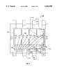
- FIG. 1 illustrates a cross-sectional top view of packaged integrated circuit with a separate circuit device mounted on a lead post.
- FIG. 2 illustrates the assembly of FIG. 1 with a plurality of wire interconnections.
- FIG. 3 illustrates a close-up cross-sectional side view of the separate circuit device placement and wire interconnection of FIG. 2.
- FIG. 4 illustrates a cross-sectional front view of the packaged integrated circuit of FIG. 1 showing the separate circuit and wire placement.
- FIG. 5 illustrates a cross-sectional rear view of the packaged integrated circuit of FIG. 1 showing the separate circuit and wire placement.
- FIG. 6 illustrates a partial cross-sectional view of a packaged integrated circuit with two additional separate circuits mounted on lead posts with wire interconnections.
- FIG. 7 illustrates a cross-sectional top view of a packaged integrated circuit with two additional separate circuits respectively mounted on two lead posts with vertical and wire interconnections.
- FIG. 8 illustrates a close-up cross-sectional view of one of the additional separate circuits of FIG. 7.
- FIG. 9 illustrates a cross-sectional top view of a packaged integrated circuit with an additional separate circuit mounted on two lead posts with vertical and metal strip interconnections.
- FIG. 10 illustrates a cross-sectional top view of a packaged integrated circuit with an additional separate circuit mounted on two lead posts with vertical and corrugated continuous lead post interconnections.
- FIG. 11 illustrates a cross-sectional top view of a packaged integrated circuit with an additional separate circuit mounted on three lead posts.
- FIG. 12 illustrates a cross-sectional top view of a packaged integrated circuit with a die pad extension and an additional separate circuit mounted on the die pad extension.
- FIG. 13 illustrates a cross-sectional top view of two co-packaged integrated circuits with respective die pad extensions and additional separate circuits mounted on the respective die pads.
- eight lead (“8L”) SOIC integrated circuit package configuration (“ICP configuration”) 100 includes a 0.091 ⁇ 0.158 inches (2.31 ⁇ 4.01 mm) semiconductor integrated circuit die 102 downset mounted on a 0.1 ⁇ 0.166 inches (2.54 ⁇ 4.22 mm) die pad 104 using conventional mounting techniques and materials within the confines of plastic encapsulant 140.
- Lead posts 106, 108, 110, 112, 114, 116, and 118 are located along two sides of the integrated circuit 102 also within the confines of plastic encapsulant 140.
- Leads 120, 122, 124, 126, 128, 130, 132, and 134 extend external to the plastic encapsulant perimeter 136 to provide external interconnection sites.
- Lead posts 106, 108, 110, 112, 114, 116, and 118 and leads 120 122, 124, 126, 128, 130, 132, and 134 may be any conductive material suitable for ICP configurations such as aluminum, copper, gold, and other metals and alloys.
- Separate circuit 138 is a planar structure, i.e. having no bottom vertical interconnections, mounted on lead post 108, which serves as a die pad for circuit 138, with conventional assembly techniques using conductive epoxy, soldering material, eutectic materials and methods, or any other suitable materials and methods.
- the circuit 138 may be mounted to lead post 108 at any time during the assembly process of ICP configuration 100 prior to encapsulation and interconnection of circuit 138 to sites in accordance with specific circuit design and layout.
- the circuit 138 represents a generic circuit which may be, for example, an integrated circuit die such as a diode or temperature protection circuitry, other ESD protection circuitry, a discrete electrical device, integrated circuit dice, a small packaged integrated circuit, or any semiconductor device not specifically mentioned.
- Circuit 138 may, for example, be connected, through electrical interconnections (not shown in FIG. 1), to integrated circuit die 102, and/or another separate circuit device (not shown), and/or a circuit or device (not shown) external to ICP configuration 100.
- FIGS. 2 and 3 illustrate circuit 138 as a two terminal device, circuit 138 may include other terminals as necessitated by the particular circuit.
- the lead posts 106, 108, 110, 112, 114, 116, and 118 are 0.014 inches (0.36 mm) wide.
- circuit 138 is a diode
- the 0.010 ⁇ 0.020 inch (0.254 ⁇ 0.508 mm) circuit 138 is attached to 0.014 ⁇ 0.050 (0.36 ⁇ 1.27 mm) lead post 108.
- the 0.091 ⁇ 0.158 inch (2.31 ⁇ 4.01 mm) integrated circuit die 102 is attached to a 0.100 ⁇ 0.166 inch (2.54 ⁇ 4.22 mm) pad 104.
- the leads 120, 122, 124, 126, 128, 130, 132, and 134 are 0.016 inches (0.406 mm) wide.
- ICP configuration 100 with circuit 138 incorporates the low cost assembly techniques of mounting and interconnecting two separate circuits (circuit 138 and integrated circuit die 102) within a single ICP configuration while avoiding monolithic approach and external approach problems. Additionally, FIGS. 1-13 show several separate circuit placements and various interconnections which illustratively demonstrate versatility aspects of the intra-package separate circuits configuration.
- wires 202 and 204 interconnect circuit 138 and lead posts 108 and 110, respectively.
- Wires 206 and 208 interconnect lead posts 108 and 110, respectively, to integrated circuit die 102.
- Wires 210, 212, 214, 216, 218, 220, and 222 interconnect lead post 106 to various integrated circuit die 102 locations such as those shown in FIG. 2.
- specific wire interconnection terminal points are shown, it will be understood by one of ordinary skill in the art in light of this description that circuit 138 may be connected to additional and/or alternative sites as required by specific circuit designs.
- circuit 138 may be electrically connected, through at least one of the leads 120, 122, 124, 126, 128, 130, 132, and 134 and/or through another separate circuit (not shown) mounted within plastic encapsulant 140, to a circuit or device external (not shown) to ICP configuration 100 without being electrically connected to integrated circuit die 102.
- circuit 138 may be mounted to additional and/or alternative sites, for example lead posts 128, 130, 132, or 134 or tie bars 142 or 144, as desired to accommodate specific designs.
- FIG. 2 and the following Figures are made by conventional stitch wire bonding or any other suitable method unless otherwise indicated.
- FIG. 3 illustrates a close-up cross-sectional side view through line 3--3 on FIG. 2 of the separate circuit device 138 placement and wire interconnections to lead posts 110 and 108.
- the height of circuit 138 is 0.010 inches (0.254 mm), and the loop height of wire interconnections 202 and 204 is 0.012 inches (0.305 mm) measured from the top plane of circuit 138. Although specific loop heights are given, other loop heights may be suitable for other packages.
- a 0.029 inch (0.737 mm) lateral separation exists between interconnection sites 302 and 304, and a 0.025 inch (0.635 mm) lateral separation exists between interconnection sites 306 and 308.
- FIG. 4 illustrates a cross-sectional front view through line 4--4 of FIG. 2 of ICP configuration 100 showing circuit 138 and wire interconnections 202 and 206 between circuit 138 and lead post 108 and from lead post 108 to integrated circuit die 102, respectively.
- FIG. 5 illustrates a cross-sectional rear view through line 5--5 of FIG. 2 of ICP configuration 100 showing the circuit 138 and interconnection placements of wires 202 and 206.
- ICP configuration 600 having multiple lead post mounted separate circuits 602 and 604 utilizing alternative connection schemes. Separate circuits 602 and 604 represent circuits such as those represented by separate circuit 138.
- ICP configuration 600 includes leads 632, 634, 636, and 638 extending from plastic encapsulant 640. ICP configuration 600 also includes circuits 602 and 604 mounted on lead posts 608 and 610, respectively. The two circuits 602 and 604 are mounted separately from integrated circuit dice 605 and 606, mounted on die pads 642 and 644, respectively.
- Conventional assembly techniques mount circuits 602 and 604 using conductive epoxy, soldering material, eutectic materials and methods, or any other suitable materials and methods.
- FIG. 6 also illustrates wire interconnections between circuit 602 and lead post 614 and ICP configuration 606 using wires 614 and 616, respectively.
- Wires 618 and 620 connect circuit 604 to lead posts 622 and 610, respectively.
- Lead posts 622 and 610 are connected to integrated circuit die 605 with wires 628 and 630, respectively.
- Lead posts 612 and 608 are connected to integrated circuit die 606 with wires 624 and 626, respectively.
- ICP configuration 600 exhibits the advantages of ICP configuration 100 and additionally provides added functional capability and versatility with circuits 602 and 604 within a common plastic encapsulant 640.
- SOIC ICP configuration 700 includes separate circuit 702.
- Separate circuits 702 and 704 are "flip chip" bonded, i.e. electrically interconnected via backside contacts using, for example, conventional bonding materials.
- Separate circuit 702 is vertically interconnected by flip chip bonding with bottom conductive contacts 714 and 716 to lead posts 706 and 708, respectively.
- Separate circuit 704 is vertically interconnected by flip chip bonding with bottom conductive contacts 718 and 720 to lead posts 710 and 712, respectively.
- the conductive contacts 714, 716, 718, and 720 are made of metal or other suitable conductive material.
- circuits are flip chip mounted on a continuous surface. However, flip chip bonded separate circuits 702 and 704 bridge between two discontinuous surfaces, lead posts 706 and 708 and lead posts 710 and 712, respectively.
- FIG. 8 illustrates a close-up cross-sectional view of circuit 702 through line 8--8 in FIG. 7.
- circuit 702 is attached between lead posts 706 and 708 with conductive materials 802 and 804.
- the conductive materials 802 and 804 are, for example conductive epoxy, soldering material, eutectic materials, or any other suitable materials and methods.
- Respective lead posts are preferably separated by a minimum gap distance to provide electrical isolation between the respective lead posts. For example, a minimum gap distance of approximately 0.005 inch (0.127 mm) is suitable for an 8L SOIC package.
- the gap between lead posts 706 and 708 prevents unnecessary mechanical strain on circuit 702 and allows adequate contact surface area between conductive contacts 714 and 716 and lead posts 706 and 708, respectively.
- Conductive materials such as conductive materials 802 and 804 also attach circuit 704 to lead posts 710 and 712.
- other vertical interconnections may be made with additional bottom conductive material.
- circuits 702 and 704 may be attached as a planar structure with interconnections provided by wire bonding or other suitable methods and materials.
- circuits 702 and 704 use a combination of vertical interconnections and wire interconnections.
- wire 730 interconnects lead post 706 to integrated circuit die 725, mounted on die pad 732, and wires 722 and 724 interconnect two separate interconnection sites on integrated circuit die 726, mounted on die pad 734.
- the vertical interconnections of circuits 702 and 704 result in a low profile circuit and eliminate wire connections between circuit 702 and lead posts 706 and 708 and between circuit 704 and lead posts 710 and 712.
- ICP configuration 700 also exhibits the additional advantages of ICP configuration 600 discussed above.
- ICP configuration 900 includes a semiconductor integrated circuit die 902 mounted on die pad 920 with conventional techniques and materials within the confines of plastic encapsulant 904.
- FIG. 9 includes separate circuit 906 vertically interconnected between lead posts 908 and 910 using vertical interconnection assembly techniques and materials as discussed above in conjunction with circuit 702 (FIGS. 7 and 8).
- Vertical interconnection between metal strip 912 and lead post 910 and 914, and vertical interconnection between metal strip 916 and lead post 914 and 918 is accomplished using conductive epoxy, soldering material, eutectic materials and methods, or with other suitable assembly materials and techniques.
- the metal strips may be any metal, for example, aluminum, copper, gold, or metal alloys.
- ICP configuration 900 offers a low profile separate circuit 906 interconnection between lead posts 908 and 910 and low profile interconnections between lead posts 910, 914, and 918 via metal strips 912 and 916. Additionally, ICP configuration 900 offers the advantages discussed above with ICP configuration 100.
- ICP configuration 1000 is identical to ICP configuration 900 excepting that metal strips 912 and 918 (FIG. 9) have been replaced with a common lead post 1002. Corrugations 1005 and 1006 reinforce grippage of plastic encapsulant 1004 to lead post 1002. In addition to improved plastic encapsulant 1004 grippage, ICP configuration 1000 offers the advantages discussed with ICP configuration 900.
- circuit 1102 may be vertically interconnected to lead posts 1104, 1106, and 1108, a planar structure with wire interconnections using assembly techniques and materials discussed above, or interconnected using a combination of vertical interconnection, planar structures, and wire interconnection.
- Circuit 1102 and lead posts 1104, 1106, and 1108 may be connected to integrated circuits dice 1112 and/or 1114 using the wire interconnection assembly techniques and materials discussed above or by flip chip bonding.
- ICP configuration 1100 may be utilized when the die pad 1110 size allows for proximately locating three or more leads. Extending lead post 1104 eliminates the processing steps associated with the addition of metal strips and wire interconnections. Other advantages discussed in conjunction with ICP configuration 1000 are applicable to ICP configuration 1100.
- the die pad 1110 configuration may be variously dimensioned to accommodate virtually any lead post arrangement allowing separate circuit bridging between multiple lead posts and sets of multiple lead posts.
- FIG. 12 a cross-sectional view of SOIC ICP configuration 1200 is illustrated.
- FIG. 12 illustrates placement of a die pad extension in an unused region between lead posts.
- the die pad extension provides an additional circuit mounting platform for additional separate circuits.
- ICP configuration 1200 includes die pad 1202 with a 0.028 ⁇ 0.016 inch (0.711 ⁇ 0.406 mm) die pad extension 1204 of a size suitable to accommodate separate circuit 1206 within plastic encapsulant 1226.
- Die pad extension 1204 is preferably formed as a co-planar, integral part of die pad 1202. After reading this disclosure, it will be understood by one of ordinary skill in the art that well-known methods may be used to fabricate die pad extension 1204.
- Lead post 1216 is preferably separated from die pad extension 1204 by at least 0.005 inches (0.127 mm) to provide electrical isolation.
- Circuit 1206 is interconnected (not shown) to integrated circuit 1228 and/or lead posts 1208, 1210, 1214, 1216, 1218, 1220, 1222, and/or 1224 with metal strips or wire interconnections using assembly techniques and materials discussed above. Circuit 1206 may be attached to die pad extension 1204 using suitable conventional materials and techniques. Additionally, circuit 1206 may be electrically connected or electrically isolated from die pad extension 1204. Bond wires 1230 and 1232 interconnect separate circuit 1206 to integrated circuit die 1228 and lead post 1214, respectively.
- ICP configuration 1200 offers the advantages discussed above in conjunction with a separate circuit enclosed within a common plastic encapsulant. Additionally, low profile advantages can be achieved through the utilization of low profile interconnections. Furthermore, ICP configuration 1200 also offers the versatile interconnectability options.
- ICP configuration 1300 includes 0.100 ⁇ 0.078 (2.54 ⁇ 1.98 mm) inch die pad 1302 with a die pad extension 1304 of a size suitable to accommodate separate circuit 1306, and 0.100 ⁇ 0.078 inch (2.54 ⁇ 1.98 mm) die pad 1308 with a die pad extension 1310 of a size suitable to accommodate separate circuit 1312 within plastic encapsulant 1334.
- Bond wires 1336 and 1338 interconnect circuit 1306 to 0.092 ⁇ 0.072 inch (2.34 ⁇ 1.83 mm) integrated circuit 1314 and lead post 1320, respectively using assembly techniques and materials discussed above.
- Bond wires 1340 and 1342 interconnect circuit 1312 to 0.092 ⁇ 0.072 inch (2.34 ⁇ 1.83 mm) integrated circuit 1316 and lead post 1322, respectively using assembly techniques and materials discussed above.
- Circuits 1306 and 1312 may be attached to die pad extensions 1304 and 1310, respectively, using suitable conventional materials and techniques. Additionally, circuits 1306 and 1312 may be electrically connected or electrically isolated from die pad extensions 1304 and 1310, respectively.
- ICP configuration 1300 offers the advantages discussed above in conjunction with a separate circuits enclosed within a common plastic encapsulant. Additionally, low profile and versatile interconnectability advantages can be achieved as discussed above with ICP configuration 1200.
- FIGS. 1, 2, 4, 5, and 9-12 each illustrate one separate circuit and FIGS. 6-8 illustrate two separate circuits
- additional separate circuits may be incorporated into the respective ICP configurations to provide desired functions.
- integrated circuits are discussed in conjunction with FIGS. 1-13, any semiconductor device, integrated or otherwise, may be used in conjunction with intra-package separate circuits.
- specific interconnection sites are illustrated in FIGS. 1-13, respectively, it will be understood by one of ordinary skill in the art after reading this description that other interconnection sites useful with specific circuits may be utilized.
- the separate circuits may be connected, through electrical interconnections, to circuits within the same package and/or to circuits external to the package.
- ICP configurations 1200 and 1300 may incorporate additional die pad extensions in unused portions of the respective ICP configuration for additional separate circuits. Die pad extensions and lead posts may also be used in combination as mounting platforms for separate circuits. Additionally, separate circuit devices may have multiple terminal sites on one or a combination surfaces.
- SOIC particular in this description or packages, for example, DIP, PDIP, ZIP, TSSOP, SOJ, SOP, TSOP, and other IC packages are suitable as well.
Abstract
Description
Claims (31)
Priority Applications (2)
| Application Number | Priority Date | Filing Date | Title |
|---|---|---|---|
| US08/556,369 US6066890A (en) | 1995-11-13 | 1995-11-13 | Separate circuit devices in an intra-package configuration and assembly techniques |
| EP96117797A EP0773586A3 (en) | 1995-11-13 | 1996-11-07 | Separate circuit devices in an intrapackage configuration and assembly techniques |
Applications Claiming Priority (1)
| Application Number | Priority Date | Filing Date | Title |
|---|---|---|---|
| US08/556,369 US6066890A (en) | 1995-11-13 | 1995-11-13 | Separate circuit devices in an intra-package configuration and assembly techniques |
Publications (1)
| Publication Number | Publication Date |
|---|---|
| US6066890A true US6066890A (en) | 2000-05-23 |
Family
ID=24221066
Family Applications (1)
| Application Number | Title | Priority Date | Filing Date |
|---|---|---|---|
| US08/556,369 Expired - Lifetime US6066890A (en) | 1995-11-13 | 1995-11-13 | Separate circuit devices in an intra-package configuration and assembly techniques |
Country Status (2)
| Country | Link |
|---|---|
| US (1) | US6066890A (en) |
| EP (1) | EP0773586A3 (en) |
Cited By (25)
| Publication number | Priority date | Publication date | Assignee | Title |
|---|---|---|---|---|
| US6229201B1 (en) * | 1997-02-18 | 2001-05-08 | The Whitaker Corporation | Integrated circuit having a parasitic resonance filter |
| US6432750B2 (en) * | 2000-06-13 | 2002-08-13 | Fairchild Korea Semiconductor Ltd. | Power module package having insulator type heat sink attached to rear surface of lead frame and manufacturing method thereof |
| US6448643B2 (en) * | 2000-05-24 | 2002-09-10 | International Rectifier Corporation | Three commonly housed diverse semiconductor dice |
| US6593622B2 (en) * | 2001-05-02 | 2003-07-15 | International Rectifier Corporation | Power mosfet with integrated drivers in a common package |
| US20030205802A1 (en) * | 2002-02-20 | 2003-11-06 | Segaram Para Kanagasabai | Method of bonding a semiconductor die without an ESD circuit and a separate ESD circuit to an external lead, and a semiconductor device made thereby |
| US20050116322A1 (en) * | 2003-07-31 | 2005-06-02 | Fumio Sando | Circuit module |
| US6922820B1 (en) * | 2000-10-12 | 2005-07-26 | Cypress Semiconductor Corp. | Circuit for generating silicon ID for PLDS |
| DE10303933B4 (en) * | 2003-01-31 | 2005-08-04 | Infineon Technologies Ag | Semiconductor device with reduced connection-induced parasitic inductance and / or capacitance |
| US20070063340A1 (en) * | 2005-07-01 | 2007-03-22 | King Owyang | Complete power management system implemented in a single surface mount package |
| US20080013298A1 (en) * | 2006-07-14 | 2008-01-17 | Nirmal Sharma | Methods and apparatus for passive attachment of components for integrated circuits |
| US20080197458A1 (en) * | 2004-11-30 | 2008-08-21 | Zhenyu Shi | Small Outline Package in Which Mosfet and Schottky Diode Being Co-Packaged |
| US20090174055A1 (en) * | 2000-06-09 | 2009-07-09 | Vishay-Siliconix | Leadless Semiconductor Packages |
| US20110133732A1 (en) * | 2009-12-03 | 2011-06-09 | Allegro Microsystems, Inc. | Methods and apparatus for enhanced frequency response of magnetic sensors |
| US8188596B2 (en) | 2007-02-09 | 2012-05-29 | Infineon Technologies Ag | Multi-chip module |
| US8629539B2 (en) | 2012-01-16 | 2014-01-14 | Allegro Microsystems, Llc | Methods and apparatus for magnetic sensor having non-conductive die paddle |
| US8951847B2 (en) | 2012-01-18 | 2015-02-10 | Intersil Americas LLC | Package leadframe for dual side assembly |
| US20150187684A1 (en) * | 2013-12-26 | 2015-07-02 | Samsung Electro-Mechanics Co., Ltd. | Semiconductor package |
| US9411025B2 (en) | 2013-04-26 | 2016-08-09 | Allegro Microsystems, Llc | Integrated circuit package having a split lead frame and a magnet |
| US9494660B2 (en) | 2012-03-20 | 2016-11-15 | Allegro Microsystems, Llc | Integrated circuit package having a split lead frame |
| CN106449587A (en) * | 2016-08-30 | 2017-02-22 | 北京握奇数据系统有限公司 | Lead frame structure |
| US9666788B2 (en) | 2012-03-20 | 2017-05-30 | Allegro Microsystems, Llc | Integrated circuit package having a split lead frame |
| US9812588B2 (en) | 2012-03-20 | 2017-11-07 | Allegro Microsystems, Llc | Magnetic field sensor integrated circuit with integral ferromagnetic material |
| US10234513B2 (en) | 2012-03-20 | 2019-03-19 | Allegro Microsystems, Llc | Magnetic field sensor integrated circuit with integral ferromagnetic material |
| DE102019121894A1 (en) * | 2019-08-14 | 2021-02-18 | Infineon Technologies Ag | Package with integrated multiple tap impedance structure |
| US10991644B2 (en) | 2019-08-22 | 2021-04-27 | Allegro Microsystems, Llc | Integrated circuit package having a low profile |
Families Citing this family (2)
| Publication number | Priority date | Publication date | Assignee | Title |
|---|---|---|---|---|
| US6548869B2 (en) | 2001-07-13 | 2003-04-15 | Cree Microwave, Inc. | Voltage limiting protection for high frequency power device |
| JP3920629B2 (en) * | 2001-11-15 | 2007-05-30 | 三洋電機株式会社 | Semiconductor device |
Citations (16)
| Publication number | Priority date | Publication date | Assignee | Title |
|---|---|---|---|---|
| GB1255073A (en) * | 1969-05-20 | 1971-11-24 | Ferranti Ltd | Improvements relating to electrical circuit assemblies |
| JPS63136838A (en) * | 1986-11-28 | 1988-06-09 | Nec Corp | Infrared-ray remote control receiver |
| US4794431A (en) * | 1986-04-21 | 1988-12-27 | International Rectifier Corporation | Package for photoactivated semiconductor device |
| EP0443044A1 (en) * | 1989-09-12 | 1991-08-28 | Kabushiki Kaisha Toshiba | Lead frame for semiconductor device and semiconductor device using the lead frame |
| US5057906A (en) * | 1989-05-22 | 1991-10-15 | Kabushiki Kaisha Toshiba | Plastic molded type semiconductor device |
| US5075758A (en) * | 1989-07-31 | 1991-12-24 | Kabushiki Kaisha Toshiba | Semiconductor device |
| EP0540926A1 (en) * | 1991-11-04 | 1993-05-12 | Motorola, Inc. | Protection circuit on a lead of a power device |
| US5245216A (en) * | 1990-09-11 | 1993-09-14 | Kabushiki Kaisha Toshiba | Plastic-molded type semiconductor device |
| US5245215A (en) * | 1982-01-11 | 1993-09-14 | Kabushiki Kaisha Toshiba | Multichip packaged semiconductor device and method for manufacturing the same |
| US5313095A (en) * | 1992-04-17 | 1994-05-17 | Mitsubishi Denki Kabushiki Kaisha | Multiple-chip semiconductor device and a method of manufacturing the same |
| WO1994011929A2 (en) * | 1992-11-06 | 1994-05-26 | Bt&D Technologies Ltd. | Optoelectronic devices |
| US5319246A (en) * | 1989-11-30 | 1994-06-07 | Mitsubishi Denki Kabushiki Kaisha | Semiconductor device having multi-layer film structure |
| JPH06232332A (en) * | 1993-02-08 | 1994-08-19 | Hitachi Ltd | Semiconductor device |
| US5399905A (en) * | 1993-01-14 | 1995-03-21 | Mitsubishi Denki Kabushiki Kaisha | Resin sealed semiconductor device including multiple current detecting resistors |
| US5442228A (en) * | 1992-04-06 | 1995-08-15 | Motorola, Inc. | Monolithic shielded integrated circuit |
| US5545922A (en) * | 1994-06-28 | 1996-08-13 | Intel Corporation | Dual sided integrated circuit chip package with offset wire bonds and support block cavities |
-
1995
- 1995-11-13 US US08/556,369 patent/US6066890A/en not_active Expired - Lifetime
-
1996
- 1996-11-07 EP EP96117797A patent/EP0773586A3/en not_active Withdrawn
Patent Citations (16)
| Publication number | Priority date | Publication date | Assignee | Title |
|---|---|---|---|---|
| GB1255073A (en) * | 1969-05-20 | 1971-11-24 | Ferranti Ltd | Improvements relating to electrical circuit assemblies |
| US5245215A (en) * | 1982-01-11 | 1993-09-14 | Kabushiki Kaisha Toshiba | Multichip packaged semiconductor device and method for manufacturing the same |
| US4794431A (en) * | 1986-04-21 | 1988-12-27 | International Rectifier Corporation | Package for photoactivated semiconductor device |
| JPS63136838A (en) * | 1986-11-28 | 1988-06-09 | Nec Corp | Infrared-ray remote control receiver |
| US5057906A (en) * | 1989-05-22 | 1991-10-15 | Kabushiki Kaisha Toshiba | Plastic molded type semiconductor device |
| US5075758A (en) * | 1989-07-31 | 1991-12-24 | Kabushiki Kaisha Toshiba | Semiconductor device |
| EP0443044A1 (en) * | 1989-09-12 | 1991-08-28 | Kabushiki Kaisha Toshiba | Lead frame for semiconductor device and semiconductor device using the lead frame |
| US5319246A (en) * | 1989-11-30 | 1994-06-07 | Mitsubishi Denki Kabushiki Kaisha | Semiconductor device having multi-layer film structure |
| US5245216A (en) * | 1990-09-11 | 1993-09-14 | Kabushiki Kaisha Toshiba | Plastic-molded type semiconductor device |
| EP0540926A1 (en) * | 1991-11-04 | 1993-05-12 | Motorola, Inc. | Protection circuit on a lead of a power device |
| US5442228A (en) * | 1992-04-06 | 1995-08-15 | Motorola, Inc. | Monolithic shielded integrated circuit |
| US5313095A (en) * | 1992-04-17 | 1994-05-17 | Mitsubishi Denki Kabushiki Kaisha | Multiple-chip semiconductor device and a method of manufacturing the same |
| WO1994011929A2 (en) * | 1992-11-06 | 1994-05-26 | Bt&D Technologies Ltd. | Optoelectronic devices |
| US5399905A (en) * | 1993-01-14 | 1995-03-21 | Mitsubishi Denki Kabushiki Kaisha | Resin sealed semiconductor device including multiple current detecting resistors |
| JPH06232332A (en) * | 1993-02-08 | 1994-08-19 | Hitachi Ltd | Semiconductor device |
| US5545922A (en) * | 1994-06-28 | 1996-08-13 | Intel Corporation | Dual sided integrated circuit chip package with offset wire bonds and support block cavities |
Cited By (53)
| Publication number | Priority date | Publication date | Assignee | Title |
|---|---|---|---|---|
| US6229201B1 (en) * | 1997-02-18 | 2001-05-08 | The Whitaker Corporation | Integrated circuit having a parasitic resonance filter |
| US6448643B2 (en) * | 2000-05-24 | 2002-09-10 | International Rectifier Corporation | Three commonly housed diverse semiconductor dice |
| US20090174055A1 (en) * | 2000-06-09 | 2009-07-09 | Vishay-Siliconix | Leadless Semiconductor Packages |
| US8928157B2 (en) | 2000-06-09 | 2015-01-06 | Vishay-Siliconix | Encapsulation techniques for leadless semiconductor packages |
| US6432750B2 (en) * | 2000-06-13 | 2002-08-13 | Fairchild Korea Semiconductor Ltd. | Power module package having insulator type heat sink attached to rear surface of lead frame and manufacturing method thereof |
| US6922820B1 (en) * | 2000-10-12 | 2005-07-26 | Cypress Semiconductor Corp. | Circuit for generating silicon ID for PLDS |
| US6593622B2 (en) * | 2001-05-02 | 2003-07-15 | International Rectifier Corporation | Power mosfet with integrated drivers in a common package |
| USRE41719E1 (en) * | 2001-05-02 | 2010-09-21 | International Rectifier Corporation | Power MOSFET with integrated drivers in a common package |
| US6933610B2 (en) | 2002-02-20 | 2005-08-23 | Silicon Pipe, Inc. | Method of bonding a semiconductor die without an ESD circuit and a separate ESD circuit to an external lead, and a semiconductor device made thereby |
| US20030205802A1 (en) * | 2002-02-20 | 2003-11-06 | Segaram Para Kanagasabai | Method of bonding a semiconductor die without an ESD circuit and a separate ESD circuit to an external lead, and a semiconductor device made thereby |
| DE10303933B4 (en) * | 2003-01-31 | 2005-08-04 | Infineon Technologies Ag | Semiconductor device with reduced connection-induced parasitic inductance and / or capacitance |
| US20050116322A1 (en) * | 2003-07-31 | 2005-06-02 | Fumio Sando | Circuit module |
| US20080197458A1 (en) * | 2004-11-30 | 2008-08-21 | Zhenyu Shi | Small Outline Package in Which Mosfet and Schottky Diode Being Co-Packaged |
| US8089139B2 (en) * | 2004-11-30 | 2012-01-03 | Alpha & Omega Semiconductor, Ltd. | Small outline package in which MOSFET and Schottky diode being co-packaged |
| US8471381B2 (en) | 2005-07-01 | 2013-06-25 | Vishay-Siliconix | Complete power management system implemented in a single surface mount package |
| US20070063341A1 (en) * | 2005-07-01 | 2007-03-22 | King Owyang | Complete power management system implemented in a single surface mount package |
| US9093359B2 (en) | 2005-07-01 | 2015-07-28 | Vishay-Siliconix | Complete power management system implemented in a single surface mount package |
| US20070063340A1 (en) * | 2005-07-01 | 2007-03-22 | King Owyang | Complete power management system implemented in a single surface mount package |
| US20100219519A1 (en) * | 2005-07-01 | 2010-09-02 | King Owyang | Complete power management system implemented in a single surface mount package |
| US8928138B2 (en) | 2005-07-01 | 2015-01-06 | Vishay-Siliconix | Complete power management system implemented in a single surface mount package |
| CN105321921B (en) * | 2006-07-14 | 2020-11-27 | 阿莱戈微系统有限责任公司 | Method and apparatus for passive attachment of components for integrated circuits |
| EP2041592A2 (en) * | 2006-07-14 | 2009-04-01 | Allegro Microsystems Inc. | Methods and apparatus for passive attachment of components for integrated circuits |
| KR101367089B1 (en) * | 2006-07-14 | 2014-02-24 | 알레그로 마이크로시스템스, 엘엘씨 | Methods and apparatus for passive attachment of components for integrated circuits |
| US20080013298A1 (en) * | 2006-07-14 | 2008-01-17 | Nirmal Sharma | Methods and apparatus for passive attachment of components for integrated circuits |
| CN105321921A (en) * | 2006-07-14 | 2016-02-10 | 阿莱戈微系统有限责任公司 | Methods and apparatus for passive attachment of components for integrated circuits |
| EP2041592B1 (en) * | 2006-07-14 | 2021-11-10 | Allegro MicroSystems, LLC | Methods and apparatus for passive attachment of components for integrated circuits |
| US9228860B2 (en) | 2006-07-14 | 2016-01-05 | Allegro Microsystems, Llc | Sensor and method of providing a sensor |
| US8188596B2 (en) | 2007-02-09 | 2012-05-29 | Infineon Technologies Ag | Multi-chip module |
| US20110133732A1 (en) * | 2009-12-03 | 2011-06-09 | Allegro Microsystems, Inc. | Methods and apparatus for enhanced frequency response of magnetic sensors |
| US9620705B2 (en) | 2012-01-16 | 2017-04-11 | Allegro Microsystems, Llc | Methods and apparatus for magnetic sensor having non-conductive die paddle |
| US10333055B2 (en) | 2012-01-16 | 2019-06-25 | Allegro Microsystems, Llc | Methods for magnetic sensor having non-conductive die paddle |
| US9299915B2 (en) | 2012-01-16 | 2016-03-29 | Allegro Microsystems, Llc | Methods and apparatus for magnetic sensor having non-conductive die paddle |
| US8629539B2 (en) | 2012-01-16 | 2014-01-14 | Allegro Microsystems, Llc | Methods and apparatus for magnetic sensor having non-conductive die paddle |
| US8951847B2 (en) | 2012-01-18 | 2015-02-10 | Intersil Americas LLC | Package leadframe for dual side assembly |
| US10230006B2 (en) | 2012-03-20 | 2019-03-12 | Allegro Microsystems, Llc | Magnetic field sensor integrated circuit with an electromagnetic suppressor |
| US11444209B2 (en) | 2012-03-20 | 2022-09-13 | Allegro Microsystems, Llc | Magnetic field sensor integrated circuit with an integrated coil enclosed with a semiconductor die by a mold material |
| US9494660B2 (en) | 2012-03-20 | 2016-11-15 | Allegro Microsystems, Llc | Integrated circuit package having a split lead frame |
| US9666788B2 (en) | 2012-03-20 | 2017-05-30 | Allegro Microsystems, Llc | Integrated circuit package having a split lead frame |
| US9812588B2 (en) | 2012-03-20 | 2017-11-07 | Allegro Microsystems, Llc | Magnetic field sensor integrated circuit with integral ferromagnetic material |
| US11961920B2 (en) | 2012-03-20 | 2024-04-16 | Allegro Microsystems, Llc | Integrated circuit package with magnet having a channel |
| US10234513B2 (en) | 2012-03-20 | 2019-03-19 | Allegro Microsystems, Llc | Magnetic field sensor integrated circuit with integral ferromagnetic material |
| US11828819B2 (en) | 2012-03-20 | 2023-11-28 | Allegro Microsystems, Llc | Magnetic field sensor integrated circuit with integral ferromagnetic material |
| US11677032B2 (en) | 2012-03-20 | 2023-06-13 | Allegro Microsystems, Llc | Sensor integrated circuit with integrated coil and element in central region of mold material |
| US10916665B2 (en) | 2012-03-20 | 2021-02-09 | Allegro Microsystems, Llc | Magnetic field sensor integrated circuit with an integrated coil |
| US9411025B2 (en) | 2013-04-26 | 2016-08-09 | Allegro Microsystems, Llc | Integrated circuit package having a split lead frame and a magnet |
| US20150187684A1 (en) * | 2013-12-26 | 2015-07-02 | Samsung Electro-Mechanics Co., Ltd. | Semiconductor package |
| KR20150075727A (en) * | 2013-12-26 | 2015-07-06 | 삼성전기주식회사 | Semiconductor package |
| US9281257B2 (en) * | 2013-12-26 | 2016-03-08 | Samsung Electro-Mechanics Co., Ltd. | Semiconductor package including a connecting member |
| CN106449587A (en) * | 2016-08-30 | 2017-02-22 | 北京握奇数据系统有限公司 | Lead frame structure |
| US11322461B2 (en) | 2019-08-14 | 2022-05-03 | Infineon Technologies Ag | Package with integrated multi-tap impedance structure |
| DE102019121894A1 (en) * | 2019-08-14 | 2021-02-18 | Infineon Technologies Ag | Package with integrated multiple tap impedance structure |
| DE102019121894B4 (en) | 2019-08-14 | 2023-07-06 | Infineon Technologies Ag | Package with integrated multi-tap impedance structure and method for making such a package |
| US10991644B2 (en) | 2019-08-22 | 2021-04-27 | Allegro Microsystems, Llc | Integrated circuit package having a low profile |
Also Published As
| Publication number | Publication date |
|---|---|
| EP0773586A2 (en) | 1997-05-14 |
| EP0773586A3 (en) | 1999-05-12 |
Similar Documents
| Publication | Publication Date | Title |
|---|---|---|
| US6066890A (en) | Separate circuit devices in an intra-package configuration and assembly techniques | |
| US6627981B2 (en) | Resin-packaged semiconductor device | |
| US6882056B2 (en) | Multi-chip package type semiconductor device | |
| US8035204B2 (en) | Large die package structures and fabrication method therefor | |
| US5894165A (en) | Leads between chips assembly | |
| JP2582013B2 (en) | Resin-sealed semiconductor device and method of manufacturing the same | |
| KR960705357A (en) | Semiconductor devices | |
| KR20020062820A (en) | Semiconductor device having stacked multi chip module structure | |
| JPH05109972A (en) | Package assembly of lead frame and integrated circuit chip | |
| KR20020055603A (en) | Dual-die integrated circuit package | |
| JPH1092972A (en) | Package for integrated circuit | |
| US6927480B2 (en) | Multi-chip package with electrical interconnection | |
| US20130200507A1 (en) | Two-sided die in a four-sided leadframe based package | |
| KR100652106B1 (en) | Circuit device | |
| JP2001156251A (en) | Semiconductor device | |
| US6753597B1 (en) | Encapsulated semiconductor package including chip paddle and leads | |
| US5719748A (en) | Semiconductor package with a bridge for chip area connection | |
| JPH0582582A (en) | Semiconductor device | |
| US20070267756A1 (en) | Integrated circuit package and multi-layer lead frame utilized | |
| JP3942495B2 (en) | Semiconductor device | |
| KR20010059916A (en) | multi chip module semiconductor package | |
| KR100235108B1 (en) | Semiconductor package | |
| KR100212392B1 (en) | Semiconductor package | |
| JP2896223B2 (en) | Resin-sealed semiconductor device | |
| JP2952286B2 (en) | Bare chipless dress package |
Legal Events
| Date | Code | Title | Description |
|---|---|---|---|
| AS | Assignment |
Owner name: SILICONIX INCORPORATED, CALIFORNIA Free format text: ASSIGNMENT OF ASSIGNORS INTEREST;ASSIGNORS:TSUI, ANTHONY C.;KASEM, Y. MOHAMMED;REEL/FRAME:007790/0652 Effective date: 19951108 |
|
| STCF | Information on status: patent grant |
Free format text: PATENTED CASE |
|
| FEPP | Fee payment procedure |
Free format text: PAYOR NUMBER ASSIGNED (ORIGINAL EVENT CODE: ASPN); ENTITY STATUS OF PATENT OWNER: LARGE ENTITY |
|
| FPAY | Fee payment |
Year of fee payment: 4 |
|
| FPAY | Fee payment |
Year of fee payment: 8 |
|
| AS | Assignment |
Owner name: COMERICA BANK, AS AGENT,MICHIGAN Free format text: SECURITY AGREEMENT;ASSIGNORS:VISHAY SPRAGUE, INC., SUCCESSOR IN INTEREST TO VISHAY EFI, INC. AND VISHAY THIN FILM, LLC;VISHAY DALE ELECTRONICS, INC.;VISHAY INTERTECHNOLOGY, INC.;AND OTHERS;REEL/FRAME:024006/0515 Effective date: 20100212 Owner name: COMERICA BANK, AS AGENT, MICHIGAN Free format text: SECURITY AGREEMENT;ASSIGNORS:VISHAY SPRAGUE, INC., SUCCESSOR IN INTEREST TO VISHAY EFI, INC. AND VISHAY THIN FILM, LLC;VISHAY DALE ELECTRONICS, INC.;VISHAY INTERTECHNOLOGY, INC.;AND OTHERS;REEL/FRAME:024006/0515 Effective date: 20100212 |
|
| AS | Assignment |
Owner name: VISHAY DALE ELECTRONICS, INC., A DELAWARE CORPORAT Free format text: RELEASE BY SECURED PARTY;ASSIGNOR:COMERICA BANK, AS AGENT, A TEXAS BANKING ASSOCIATION (FORMERLY A MICHIGAN BANKING CORPORATION);REEL/FRAME:025489/0184 Effective date: 20101201 Owner name: SILICONIX INCORPORATED, A DELAWARE CORPORATION, PE Free format text: RELEASE BY SECURED PARTY;ASSIGNOR:COMERICA BANK, AS AGENT, A TEXAS BANKING ASSOCIATION (FORMERLY A MICHIGAN BANKING CORPORATION);REEL/FRAME:025489/0184 Effective date: 20101201 Owner name: YOSEMITE INVESTMENT, INC., AN INDIANA CORPORATION, Free format text: RELEASE BY SECURED PARTY;ASSIGNOR:COMERICA BANK, AS AGENT, A TEXAS BANKING ASSOCIATION (FORMERLY A MICHIGAN BANKING CORPORATION);REEL/FRAME:025489/0184 Effective date: 20101201 Owner name: VISHAY MEASUREMENTS GROUP, INC., A DELAWARE CORPOR Free format text: RELEASE BY SECURED PARTY;ASSIGNOR:COMERICA BANK, AS AGENT, A TEXAS BANKING ASSOCIATION (FORMERLY A MICHIGAN BANKING CORPORATION);REEL/FRAME:025489/0184 Effective date: 20101201 Owner name: VISHAY VITRAMON, INCORPORATED, A DELAWARE CORPORAT Free format text: RELEASE BY SECURED PARTY;ASSIGNOR:COMERICA BANK, AS AGENT, A TEXAS BANKING ASSOCIATION (FORMERLY A MICHIGAN BANKING CORPORATION);REEL/FRAME:025489/0184 Effective date: 20101201 Owner name: VISHAY GENERAL SEMICONDUCTOR, LLC, F/K/A GENERAL S Free format text: RELEASE BY SECURED PARTY;ASSIGNOR:COMERICA BANK, AS AGENT, A TEXAS BANKING ASSOCIATION (FORMERLY A MICHIGAN BANKING CORPORATION);REEL/FRAME:025489/0184 Effective date: 20101201 Owner name: VISHAY INTERTECHNOLOGY, INC., A DELAWARE CORPORATI Free format text: RELEASE BY SECURED PARTY;ASSIGNOR:COMERICA BANK, AS AGENT, A TEXAS BANKING ASSOCIATION (FORMERLY A MICHIGAN BANKING CORPORATION);REEL/FRAME:025489/0184 Effective date: 20101201 Owner name: VISHAY SPRAGUE, INC., SUCCESSOR-IN-INTEREST TO VIS Free format text: RELEASE BY SECURED PARTY;ASSIGNOR:COMERICA BANK, AS AGENT, A TEXAS BANKING ASSOCIATION (FORMERLY A MICHIGAN BANKING CORPORATION);REEL/FRAME:025489/0184 Effective date: 20101201 |
|
| AS | Assignment |
Owner name: JPMORGAN CHASE BANK, N.A., AS ADMINISTRATIVE AGENT, TEXAS Free format text: SECURITY AGREEMENT;ASSIGNORS:VISHAY INTERTECHNOLOGY, INC.;VISHAY DALE ELECTRONICS, INC.;SILICONIX INCORPORATED;AND OTHERS;REEL/FRAME:025675/0001 Effective date: 20101201 Owner name: JPMORGAN CHASE BANK, N.A., AS ADMINISTRATIVE AGENT Free format text: SECURITY AGREEMENT;ASSIGNORS:VISHAY INTERTECHNOLOGY, INC.;VISHAY DALE ELECTRONICS, INC.;SILICONIX INCORPORATED;AND OTHERS;REEL/FRAME:025675/0001 Effective date: 20101201 |
|
| FPAY | Fee payment |
Year of fee payment: 12 |
|
| AS | Assignment |
Owner name: VISHAY EFI, INC., VERMONT Free format text: RELEASE BY SECURED PARTY;ASSIGNOR:JPMORGAN CHASE BANK, N.A., AS ADMINISTRATIVE AGENT;REEL/FRAME:049826/0312 Effective date: 20190716 Owner name: VISHAY TECHNO COMPONENTS, LLC, VERMONT Free format text: RELEASE BY SECURED PARTY;ASSIGNOR:JPMORGAN CHASE BANK, N.A., AS ADMINISTRATIVE AGENT;REEL/FRAME:049826/0312 Effective date: 20190716 Owner name: VISHAY SPRAGUE, INC., VERMONT Free format text: RELEASE BY SECURED PARTY;ASSIGNOR:JPMORGAN CHASE BANK, N.A., AS ADMINISTRATIVE AGENT;REEL/FRAME:049826/0312 Effective date: 20190716 Owner name: VISHAY DALE ELECTRONICS, INC., NEBRASKA Free format text: RELEASE BY SECURED PARTY;ASSIGNOR:JPMORGAN CHASE BANK, N.A., AS ADMINISTRATIVE AGENT;REEL/FRAME:049826/0312 Effective date: 20190716 Owner name: VISHAY INTERTECHNOLOGY, INC., PENNSYLVANIA Free format text: RELEASE BY SECURED PARTY;ASSIGNOR:JPMORGAN CHASE BANK, N.A., AS ADMINISTRATIVE AGENT;REEL/FRAME:049826/0312 Effective date: 20190716 Owner name: SILICONIX INCORPORATED, CALIFORNIA Free format text: RELEASE BY SECURED PARTY;ASSIGNOR:JPMORGAN CHASE BANK, N.A., AS ADMINISTRATIVE AGENT;REEL/FRAME:049826/0312 Effective date: 20190716 Owner name: DALE ELECTRONICS, INC., NEBRASKA Free format text: RELEASE BY SECURED PARTY;ASSIGNOR:JPMORGAN CHASE BANK, N.A., AS ADMINISTRATIVE AGENT;REEL/FRAME:049826/0312 Effective date: 20190716 Owner name: VISHAY VITRAMON, INC., VERMONT Free format text: RELEASE BY SECURED PARTY;ASSIGNOR:JPMORGAN CHASE BANK, N.A., AS ADMINISTRATIVE AGENT;REEL/FRAME:049826/0312 Effective date: 20190716 Owner name: SPRAGUE ELECTRIC COMPANY, VERMONT Free format text: RELEASE BY SECURED PARTY;ASSIGNOR:JPMORGAN CHASE BANK, N.A., AS ADMINISTRATIVE AGENT;REEL/FRAME:049826/0312 Effective date: 20190716 |