US6066545A - Birdsbeak encroachment using combination of wet and dry etch for isolation nitride - Google Patents
Birdsbeak encroachment using combination of wet and dry etch for isolation nitride Download PDFInfo
- Publication number
- US6066545A US6066545A US09/207,086 US20708698A US6066545A US 6066545 A US6066545 A US 6066545A US 20708698 A US20708698 A US 20708698A US 6066545 A US6066545 A US 6066545A
- Authority
- US
- United States
- Prior art keywords
- nitride
- birdsbeak
- encroachment
- nitride layer
- layer
- Prior art date
- Legal status (The legal status is an assumption and is not a legal conclusion. Google has not performed a legal analysis and makes no representation as to the accuracy of the status listed.)
- Expired - Lifetime
Links
Images


Classifications
-
- H—ELECTRICITY
- H01—ELECTRIC ELEMENTS
- H01L—SEMICONDUCTOR DEVICES NOT COVERED BY CLASS H10
- H01L21/00—Processes or apparatus adapted for the manufacture or treatment of semiconductor or solid state devices or of parts thereof
- H01L21/70—Manufacture or treatment of devices consisting of a plurality of solid state components formed in or on a common substrate or of parts thereof; Manufacture of integrated circuit devices or of parts thereof
- H01L21/71—Manufacture of specific parts of devices defined in group H01L21/70
- H01L21/76—Making of isolation regions between components
- H01L21/762—Dielectric regions, e.g. EPIC dielectric isolation, LOCOS; Trench refilling techniques, SOI technology, use of channel stoppers
- H01L21/76202—Dielectric regions, e.g. EPIC dielectric isolation, LOCOS; Trench refilling techniques, SOI technology, use of channel stoppers using a local oxidation of silicon, e.g. LOCOS, SWAMI, SILO
Definitions
- the present invention relates to integrated circuit structures and fabrication methods and specifically to improving the encroachment of the field oxide into the active areas and reduce stress in the silicon near the field oxide.
- LOCOS process or Local Oxidation of Silicon. This technique depends on the fact that silicon nitride is impervious to oxygen diffusion and can be used as a mask against oxidation. Thus, if a bare silicon wafer is covered with a nitride layer which then has openings etched in it, a subsequent oxidation step will grow oxide only where the nitride is removed.
- a problem with the conventional LOCOS method is the stress caused in the silicon substrate due to a) the mismatch of thermal expansion coefficients of the substrate and of the nitride, and b) the volumetric increase of the growing oxide. Because of the high stress at the nitride/silicon interface, dislocations in the silicon at corners of the openings in the nitride layer occur often durinc subsequent oxide growth. To prevent this problem, as shown in FIG. 2, a thin layer of thermal oxide 110 (known as a pad or buffer oxide) is generally used between the nitride 120 and the silicon substrate 100. When the dielectric isolation area 130 is subsequently formed, oxygen diffusion through the pad oxide and along the interface can cause additional oxide growth under the nitride. This additional oxide growth gives rise to an encroachment area 140, also known as a "birdsbeak", of the active area.
- encroachment area 140 also known as a "birdsbeak" of the active area.
- the encroachment area affects device performance in two significant ways. First, the encroachment reduces the active width of the device, thereby reducing the amount of current the transistor can drive. Second, the field oxidation causes subsequent field implant of dopants to diffuse out of the edge of the active region. If the transistor is narrow enough, the diffused dopant will increase the threshold voltage of the device, thereby reducing its current drive.
- the current process used for LOCOS is good for up to 16 M DRAM (0.5 micron design rule).
- the issue arises of a large bird's beak at the edge of a long moat which is critical for contact to the storage node.
- the moat area has been so encroached by the oxide that overlap of the storage node contact area is minimal.
- the encroachment is reduced, allowing the moat to completely overlap the contact area
- a thick birdsbeak is not good for the storage node contact (SNCT) etch, but a simple thick nitride does not solve the problem because it induces stress leading to silicon crystal damage. Thus, it is desirable to reduce the birdsbeak without creating stress.
- SNCT storage node contact
- the present application discloses a technique for reducing active area encroachment (birdsbeak) by using a "trapezoid nitride process.”
- This process uses the combination of a polysilicon hard mask and wet etch for the nitride, followed by a dry etch to produce a trapezoidal nitride profile as shown in FIG. 7. Having a nitride that is thinner at the edges reduces stress at the interface, particularly in the horizontal direction (the active area width).
- FIG. 1 shows a process flow for fabrication of LOCOS isolation using the disclosed trapezoidal nitride layer.
- FIG. 2 shows a conventional structure with LOCOS isolation and the resultant active area encroachment (birdsbeak).
- FIG. 3 shows a prior solution to the birdsbeak encroachment.
- FIGS. 4-7 illustrate various stages in the disclosed process.
- FIG. 8A shows how the moat area is decreased in previous methods, making contact with the storage node more difficult
- FIG. 8B shows the moat area and storage node under the disclosed method, where the contact overlap is much greater.
- FIGS. 9A-9B show LOCOS stress simulations for a conventional nitride with a thickness of 130 nm and a trapezoidal-shaped nitride with a main thickness of 130 nm and with 30 nm removed by the isotropic etch.
- FIGS. 10A-10D show LOCOS stress simulations for a conventional nitride with a thickness of 160 nm and a trapezoidal-shaped nitride with a main thickness of 160 nm and with 60, 80, and 100 nm respectively removed by the isotropic etch.
- FIGS. 11A-11B show LOCOS stress simulations for a conventional nitride with a thickness of 200 nm and a trapezoidal-shaped nitride with a main thickness of 200 nm and with 100 nm removed by the isotropic etch.
- FIG. 12 shows a graph of nitride thickness versus tensile stress for both conventional nitrides and the disclosed trapezoidal-shaped nitrides.
- FIG. 13 shows a graph of the thickness of the nitride layer at the edges of the layer versus the compressive stress.
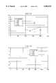
- FIG. 1 is a process flow for fabrication of an integrated circuit device. The steps in FIG. 1 will now be discussed in an overview of the disclosed invention, with reference to FIGS. 4-7. Details and specific examples are discussed below in a sample embodiment.
- the first step in the process involves forming (step 110) a thin dielectric layer 210 over a semiconductor substrate 200, followed by deposition (step 120) of nitride layer 220.
- a hardmask layer 230 is formed and patterned (step 130) over nitride layer 220, resulting in the structure shown in FIG. 4.
- Nitride layer 220 is then wet etched, (step 140), resulting in the structure shown in FIG. 5. Nitride layer 220 is then dry etched (step 150), resulting in the structure shown in FIG. 6. This trapezoidal nitride layer is used to mask the oxidation step (step 160), and provides better control of the encroachment, as well as the other advantages listed above.
- FIG. 7 shows the wafer surface after oxidation, after which the nitride layer is stripped and the remaining integration proceeds according to methods known in the art.
- semiconductor substrate 200 is silicon.
- Thin dielectric layer 210 is silicon dioxide, grown 8-11 nm thick in this sample embodiment.
- Silicon nitride layer 220 is 100-200 nm thick, deposited by a low pressure-chemical vapor deposition (LPCVD) process using mixtures of dichlorosilane and ammonia, and a deposition temperature of 700-900 degrees C
- Polysilicon layer 230 is deposited to a thickness of 100 nm and patterned with resist, which is then removed.
- LPCVD low pressure-chemical vapor deposition
- an isotropic wet etch is performed on silicon nitride layer 220.
- the etchant in this sample embodiment is phosphoric acid (H3PO4) preferably at 145 degrees C, although it can be performed in the range of 140-200 degrees C., to remove the corner of the nitride at the edges of the hardmask.
- the wet etch is performed in an automated wet bench process, with the sequence (a.) HF @ 25 degrees C., (b.) de-ionized water rinse, (c.) H3PO4 @ 145 degrees C., (d.) H3PO4 @ 145 degrees C.; (e.) de-ionized water rinse; (f.) spin dry.
- an anisotropic dry etch is performed on silicon nitride layer 240.
- a plasma etch process which is rich in atomic fluorine is used, such as a CF4-O2 plasma. This etch would typically be performed at a frequency of 13.56 MHz and an operating pressure of 200 mT.
- CF4-O2 plasma a plasma etch process which is rich in atomic fluorine
- This etch would typically be performed at a frequency of 13.56 MHz and an operating pressure of 200 mT.
- suitable dry etch processes are readily apparent to one skilled in the art.
- the oxide is then grown by known methods, giving the structure shown in FIG. 7.
- TEOS tetraethylorthosilicate
- semiconductor substrate is silicon-germanium rather than silicon as in the sample embodiment. Other conditions remain similar to those stated above.
- silicon nitride layer 220 is deposited by plasma-enhanced-chemical vapor deposition process. The process is run at 300-400 degrees C. using a mixture of argon or helium, silane, and either ammonia or nitrogen. Other conditions remain similar to those stated above.
- FIGS. 9A-9B show LOCOS stress simulations for a conventional nitride with a thickness of 130 nm and a trapezoidal-shaped nitride with a main thickness of 130 nm and with 30 nm removed by the isotropic etch.
- FIGS. 10A-10D show LOCOS stress simulations for a conventional nitride with a thickness of 160 nm and a trapezoidal-shaped nitride with a main thickness of 160 nm and with 60, 80, and 100 nm respectively removed by the isotropic etch.
- FIGS. 11A-11B show LOCOS stress simulations for a conventional nitride with a thickness of 200 nm and a trapezoidal-shaped nitride with a main thickness of 200 nm and with 100 nm removed by the isotropic etch.
- FIG. 12 shows a graph of nitride thickness versus tensile stress for both conventional nitrides and the disclosed trapezoidal-shaped nitrides.
- Baseline for conventional nitrides is shown by the black line, while values for various amounts removed by the isotropic etch are shown by the coded points.
- FIG. 13 shows a graph of the thickness of the nitride layer removed at the edges of the layer versus the compressive stress. Two or more values are given for each thickness, that of a conventional layer with no trapezoidal etch done, and for the disclosed process in which a trapezoidal shape is formed.
- the disclosed process is also applicable to other modified LOCOS processes, such as poly-buffered LOCOS or Sidewall-Masked Isolation (SWAMI).
- modified LOCOS processes such as poly-buffered LOCOS or Sidewall-Masked Isolation (SWAMI).
Abstract
A technique for reducing active area encroachment (birdsbeak) by using a polysilicon hard mask combined with both wet and dry etch for the isolation nitride. This process forms a thinner layer of nitride adjacent the openings for oxide growth, which reduces stress at the silicon/nitride interface. The advantages include control over birdsbeak, reliable gate oxide quality, low junction leakage current, an improved active area, improved isolation, low peripheral junction leakage, and higher field transistor threshold voltage.
Description
This application claims priority under 35 USC § 119 (e) (1) of provisional application number 60/067,986, filed Dec. 9, 1997.
The present invention relates to integrated circuit structures and fabrication methods and specifically to improving the encroachment of the field oxide into the active areas and reduce stress in the silicon near the field oxide.
A common isolation technique for integrated circuits is the so-called LOCOS process, or Local Oxidation of Silicon. This technique depends on the fact that silicon nitride is impervious to oxygen diffusion and can be used as a mask against oxidation. Thus, if a bare silicon wafer is covered with a nitride layer which then has openings etched in it, a subsequent oxidation step will grow oxide only where the nitride is removed.
A problem with the conventional LOCOS method is the stress caused in the silicon substrate due to a) the mismatch of thermal expansion coefficients of the substrate and of the nitride, and b) the volumetric increase of the growing oxide. Because of the high stress at the nitride/silicon interface, dislocations in the silicon at corners of the openings in the nitride layer occur often durinc subsequent oxide growth. To prevent this problem, as shown in FIG. 2, a thin layer of thermal oxide 110 (known as a pad or buffer oxide) is generally used between the nitride 120 and the silicon substrate 100. When the dielectric isolation area 130 is subsequently formed, oxygen diffusion through the pad oxide and along the interface can cause additional oxide growth under the nitride. This additional oxide growth gives rise to an encroachment area 140, also known as a "birdsbeak", of the active area.
The encroachment area (birdsbeak) affects device performance in two significant ways. First, the encroachment reduces the active width of the device, thereby reducing the amount of current the transistor can drive. Second, the field oxidation causes subsequent field implant of dopants to diffuse out of the edge of the active region. If the transistor is narrow enough, the diffused dopant will increase the threshold voltage of the device, thereby reducing its current drive.
One previous solution to the birdsbeak intrusion has been to form a nitride sidewall, as shown in FIG. 3, to prevent oxygen diffusion through the pad oxide.
The current process used for LOCOS is good for up to 16 M DRAM (0.5 micron design rule). In the 64 M DRAM level (0.3 micron design rule), the issue arises of a large bird's beak at the edge of a long moat which is critical for contact to the storage node. As seen in FIG. 8A, the moat area has been so encroached by the oxide that overlap of the storage node contact area is minimal. In FIG. 8B, under the disclosed method, the encroachment is reduced, allowing the moat to completely overlap the contact area
A thick birdsbeak is not good for the storage node contact (SNCT) etch, but a simple thick nitride does not solve the problem because it induces stress leading to silicon crystal damage. Thus, it is desirable to reduce the birdsbeak without creating stress.
Modification of Isolation Nitride Etch
The present application discloses a technique for reducing active area encroachment (birdsbeak) by using a "trapezoid nitride process." This process uses the combination of a polysilicon hard mask and wet etch for the nitride, followed by a dry etch to produce a trapezoidal nitride profile as shown in FIG. 7. Having a nitride that is thinner at the edges reduces stress at the interface, particularly in the horizontal direction (the active area width).
The advantages of the disclosed methods and devices formed by the disclosed methods include:
does not cause dislocation in the substrate;
uses known methods and tools;
provides reliable gate oxide quality;
provides low junction leakage current;
simulations achieved 9 percent stress reduction in silicon layer;
improved active area;
improved isolation with low peripheral junction leakage and higher field transistor threshold voltage;
improved yield in probe test, including;
designed size of active area, as seen in the area masked, can be decreased since there is less encroachment; and
cell-to-cell spacing can be decreased.
The disclosed inventions will be described with reference to the accompanying drawings, which show important sample embodiments of the invention and which are incorporated in the specification hereof by reference, wherein:
FIG. 1 shows a process flow for fabrication of LOCOS isolation using the disclosed trapezoidal nitride layer.
FIG. 2 shows a conventional structure with LOCOS isolation and the resultant active area encroachment (birdsbeak).
FIG. 3 shows a prior solution to the birdsbeak encroachment.
FIGS. 4-7 illustrate various stages in the disclosed process.
FIG. 8A shows how the moat area is decreased in previous methods, making contact with the storage node more difficult;
FIG. 8B shows the moat area and storage node under the disclosed method, where the contact overlap is much greater.
FIGS. 9A-9B show LOCOS stress simulations for a conventional nitride with a thickness of 130 nm and a trapezoidal-shaped nitride with a main thickness of 130 nm and with 30 nm removed by the isotropic etch.
FIGS. 10A-10D show LOCOS stress simulations for a conventional nitride with a thickness of 160 nm and a trapezoidal-shaped nitride with a main thickness of 160 nm and with 60, 80, and 100 nm respectively removed by the isotropic etch.
FIGS. 11A-11B show LOCOS stress simulations for a conventional nitride with a thickness of 200 nm and a trapezoidal-shaped nitride with a main thickness of 200 nm and with 100 nm removed by the isotropic etch.
FIG. 12 shows a graph of nitride thickness versus tensile stress for both conventional nitrides and the disclosed trapezoidal-shaped nitrides.
FIG. 13 shows a graph of the thickness of the nitride layer at the edges of the layer versus the compressive stress.
The numerous innovative teachings of the present application will be described with particular reference to the presently preferred embodiment. However, it should be understood that this class of embodiments provides only a few examples of the many advantageous uses of the innovative teachings herein. In general, statements made in the specification of the present application do not necessarily delimit any of the various claimed inventions. Moreover, some statements may apply to some inventive features but not to others.
Overview of Isolation Nitride Etch
FIG. 1 is a process flow for fabrication of an integrated circuit device. The steps in FIG. 1 will now be discussed in an overview of the disclosed invention, with reference to FIGS. 4-7. Details and specific examples are discussed below in a sample embodiment.
The first step in the process involves forming (step 110) a thin dielectric layer 210 over a semiconductor substrate 200, followed by deposition (step 120) of nitride layer 220. A hardmask layer 230 is formed and patterned (step 130) over nitride layer 220, resulting in the structure shown in FIG. 4.
Sample Embodiment
Details and specific examples of one embodiment of the process flow will now be discussed.
Referring to FIG. 4, semiconductor substrate 200 is silicon. Thin dielectric layer 210 is silicon dioxide, grown 8-11 nm thick in this sample embodiment. Silicon nitride layer 220 is 100-200 nm thick, deposited by a low pressure-chemical vapor deposition (LPCVD) process using mixtures of dichlorosilane and ammonia, and a deposition temperature of 700-900 degrees C Polysilicon layer 230 is deposited to a thickness of 100 nm and patterned with resist, which is then removed.
In FIG. 5, an isotropic wet etch is performed on silicon nitride layer 220. The etchant in this sample embodiment is phosphoric acid (H3PO4) preferably at 145 degrees C, although it can be performed in the range of 140-200 degrees C., to remove the corner of the nitride at the edges of the hardmask. The wet etch is performed in an automated wet bench process, with the sequence (a.) HF @ 25 degrees C., (b.) de-ionized water rinse, (c.) H3PO4 @ 145 degrees C., (d.) H3PO4 @ 145 degrees C.; (e.) de-ionized water rinse; (f.) spin dry.
Referring to FIG. 6, an anisotropic dry etch is performed on silicon nitride layer 240. For selectivity of the nitride to the underlying oxide, a plasma etch process which is rich in atomic fluorine is used, such as a CF4-O2 plasma. This etch would typically be performed at a frequency of 13.56 MHz and an operating pressure of 200 mT. However, a variety of suitable dry etch processes are readily apparent to one skilled in the art. The oxide is then grown by known methods, giving the structure shown in FIG. 7.
Alternative Embodiment: TEOS Hardmask
In an alternative embodiment, tetraethylorthosilicate (TEOS) is used in a low pressure CVD process to form the hardmask.
Alternative Embodiment: Silicon-Germanium Substrate
In an alternative embodiment, semiconductor substrate is silicon-germanium rather than silicon as in the sample embodiment. Other conditions remain similar to those stated above.
Alternative Embodiment: PECVD Nitride Deposition
In an alternative embodiment, silicon nitride layer 220 is deposited by plasma-enhanced-chemical vapor deposition process. The process is run at 300-400 degrees C. using a mixture of argon or helium, silane, and either ammonia or nitrogen. Other conditions remain similar to those stated above.
Simulations
Simulations of the disclosed process have been run, and the results are shown in FIGS. 9-13.
FIGS. 9A-9B show LOCOS stress simulations for a conventional nitride with a thickness of 130 nm and a trapezoidal-shaped nitride with a main thickness of 130 nm and with 30 nm removed by the isotropic etch.
FIGS. 10A-10D show LOCOS stress simulations for a conventional nitride with a thickness of 160 nm and a trapezoidal-shaped nitride with a main thickness of 160 nm and with 60, 80, and 100 nm respectively removed by the isotropic etch.
FIGS. 11A-11B show LOCOS stress simulations for a conventional nitride with a thickness of 200 nm and a trapezoidal-shaped nitride with a main thickness of 200 nm and with 100 nm removed by the isotropic etch.
FIG. 12 shows a graph of nitride thickness versus tensile stress for both conventional nitrides and the disclosed trapezoidal-shaped nitrides. Baseline for conventional nitrides is shown by the black line, while values for various amounts removed by the isotropic etch are shown by the coded points.
FIG. 13 shows a graph of the thickness of the nitride layer removed at the edges of the layer versus the compressive stress. Two or more values are given for each thickness, that of a conventional layer with no trapezoidal etch done, and for the disclosed process in which a trapezoidal shape is formed.
It is evident from these results that varying the removal of nitride at the edge of the layer does not uniformly cause lowered stress, but that careful selection of amounts of nitride to be removed at the edges can provide a beneficial result. In this example, for a nitride with a thickness of 160 nm, reduction of the edge by 800 nm produces a lowering of compressive stress from 13.9 to 13 (a 6.5 percent reduction) and of tensile stress from 6.5 to 5.7 (a 12 percent reduction).
Modifications and Variations
As will be recognized by those skilled in the art, the innovative concepts described in the present application can be modified and varied over a tremendous range of applications, and accordingly the scope of patented subject matter is not limited by any of the specific exemplary teachings given, but is only defined by the issued claims.
The disclosed process is also applicable to other modified LOCOS processes, such as poly-buffered LOCOS or Sidewall-Masked Isolation (SWAMI).
Similarly, it will be readily recognized that the described process steps can also be embedded into hybrid process flows, such as BiCMOS or smart-power processes.
Claims (4)
1. A fabrication method for intergrated circuits, comprising the steps of:
(a.) forming a nitride layer over a thermal oxide which overlies a semiconductor material;
(b.) forming a hardmask layer over said nitride layer;
(c.) forming openings in said hardmask layer in locations where isolation structures are desired;
(d.) partially etching said nitride layer, through said openings in said hardmask layer, with a primarily isotropic etch; and
(e.) after said step (d.), anisotropically etching said nitride layer through said openings in said hardmask layer, to expose portions of said thermal oxide.
2. The fabrication method of claim 1, wherein said nitride layer is silicon nitride.
3. The fabrication method of claim 1, wherein said semiconductor material comprises monocrystalline silicon.
4. The fabrication method of claim 1, further comprising (f.) oxidizing said semiconductor material to form field oxides,
using remaining portions of said nitride layer as a mask; whereby said field oxides have a reduced birdsbeak encroachment into said active area.
Priority Applications (1)
| Application Number | Priority Date | Filing Date | Title |
|---|---|---|---|
| US09/207,086 US6066545A (en) | 1997-12-09 | 1998-12-07 | Birdsbeak encroachment using combination of wet and dry etch for isolation nitride |
Applications Claiming Priority (2)
| Application Number | Priority Date | Filing Date | Title |
|---|---|---|---|
| US6798697P | 1997-12-09 | 1997-12-09 | |
| US09/207,086 US6066545A (en) | 1997-12-09 | 1998-12-07 | Birdsbeak encroachment using combination of wet and dry etch for isolation nitride |
Publications (1)
| Publication Number | Publication Date |
|---|---|
| US6066545A true US6066545A (en) | 2000-05-23 |
Family
ID=26748459
Family Applications (1)
| Application Number | Title | Priority Date | Filing Date |
|---|---|---|---|
| US09/207,086 Expired - Lifetime US6066545A (en) | 1997-12-09 | 1998-12-07 | Birdsbeak encroachment using combination of wet and dry etch for isolation nitride |
Country Status (1)
| Country | Link |
|---|---|
| US (1) | US6066545A (en) |
Cited By (75)
| Publication number | Priority date | Publication date | Assignee | Title |
|---|---|---|---|---|
| US6211046B1 (en) * | 1998-07-30 | 2001-04-03 | Sanyo Electric Co., Ltd. | Method of manufacturing a semiconductor device |
| US6239003B1 (en) * | 1998-06-16 | 2001-05-29 | Texas Instruments Incorporated | Method of simultaneous fabrication of isolation and gate regions in a semiconductor device |
| US6562723B1 (en) * | 1999-10-29 | 2003-05-13 | Advanced Micro Devices, Inc. | Hybrid stack method for patterning source/drain areas |
| US20040238914A1 (en) * | 2003-05-30 | 2004-12-02 | International Business Machines Corporation | STI stress modification by nitrogen plasma treatment for improving performance in small width devices |
| US20040256700A1 (en) * | 2003-06-17 | 2004-12-23 | International Business Machines Corporation | High-performance CMOS devices on hybrid crystal oriented substrates |
| US20040266151A1 (en) * | 2003-06-30 | 2004-12-30 | Kwan-Yong Lim | Method for fabricating gate-electrode of semiconductor device with use of hard mask |
| US20040262784A1 (en) * | 2003-06-30 | 2004-12-30 | International Business Machines Corporation | High performance cmos device structures and method of manufacture |
| US20050054145A1 (en) * | 2003-09-09 | 2005-03-10 | International Business Machines Corporation | Method for reduced n+ diffusion in strained si on sige substrate |
| US20050054148A1 (en) * | 2003-09-10 | 2005-03-10 | International Business Machines Corporation | METHOD AND STRUCTURE FOR IMPROVED MOSFETs USING POLY/SILICIDE GATE HEIGHT CONTROL |
| US20050059214A1 (en) * | 2003-09-16 | 2005-03-17 | International Business Machines Corporation | Method and structure of vertical strained silicon devices |
| US6869866B1 (en) | 2003-09-22 | 2005-03-22 | International Business Machines Corporation | Silicide proximity structures for CMOS device performance improvements |
| US20050064646A1 (en) * | 2003-09-23 | 2005-03-24 | Dureseti Chidambarrao | NFETs using gate induced stress modulation |
| US20050064686A1 (en) * | 2003-09-23 | 2005-03-24 | Dureseti Chidambarrao | Strained silicon on relaxed sige film with uniform misfit dislocation density |
| US20050082616A1 (en) * | 2003-10-20 | 2005-04-21 | Huajie Chen | High performance stress-enhanced MOSFETs using Si:C and SiGe epitaxial source/drain and method of manufacture |
| US20050085022A1 (en) * | 2003-10-20 | 2005-04-21 | Dureseti Chidambarrao | Strained dislocation-free channels for CMOS and method of manufacture |
| US6887751B2 (en) | 2003-09-12 | 2005-05-03 | International Business Machines Corporation | MOSFET performance improvement using deformation in SOI structure |
| US20050093076A1 (en) * | 2003-11-05 | 2005-05-05 | International Business Machines Corporation | METHOD AND STRUCTURE FOR FORMING STRAINED Si FOR CMOS DEVICES |
| US20050098829A1 (en) * | 2003-11-06 | 2005-05-12 | Doris Bruce B. | High mobility CMOS circuits |
| US20050104131A1 (en) * | 2003-11-19 | 2005-05-19 | Dureseti Chidambarrao | Silicon device on Si:C-OI and SGOI and method of manufacture |
| US20050106799A1 (en) * | 2003-11-14 | 2005-05-19 | International Business Machines Corporation | Stressed semiconductor device structures having granular semiconductor material |
| US20050106790A1 (en) * | 2003-11-13 | 2005-05-19 | Kangguo Cheng | Strained silicon on a SiGe on SOI substrate |
| US20050130358A1 (en) * | 2003-12-12 | 2005-06-16 | Dureseti Chidambarrao | Strained finFETs and method of manufacture |
| US20050158955A1 (en) * | 2004-01-16 | 2005-07-21 | International Business Machines Corporation | Method and apparatus to increase strain effect in a transistor channel |
| US20050189589A1 (en) * | 2004-02-27 | 2005-09-01 | International Business Machines Corporation | Hybrid soi/bulk semiconductor transistors |
| US20050194699A1 (en) * | 2004-03-03 | 2005-09-08 | International Business Machines Corporation | Mobility enhanced cmos devices |
| US20050236668A1 (en) * | 2004-04-23 | 2005-10-27 | International Business Machines Corporation | STRUCTURES AND METHODS FOR MANUFACTURING OF DISLOCATION FREE STRESSED CHANNELS IN BULK SILICON AND SOI CMOS DEVICES BY GATE STRESS ENGINEERING WITH SiGe AND/OR Si:C |
| US20050269561A1 (en) * | 2004-06-03 | 2005-12-08 | Dureseti Chidambarrao | Strained Si on multiple materials for bulk or SOI substrates |
| US20050277271A1 (en) * | 2004-06-09 | 2005-12-15 | International Business Machines Corporation | RAISED STI PROCESS FOR MULTIPLE GATE OX AND SIDEWALL PROTECTION ON STRAINED Si/SGOI STRUCTURE WITH ELEVATED SOURCE/DRAIN |
| US20050285187A1 (en) * | 2004-06-24 | 2005-12-29 | International Business Machines Corporation | Strained-silicon CMOS device and method |
| US20050285192A1 (en) * | 2004-06-29 | 2005-12-29 | International Business Machines Corporation | Structures and methods for manufacturing p-type mosfet withgraded embedded silicon-germanium source-drain and/or extension |
| US20060001089A1 (en) * | 2004-07-02 | 2006-01-05 | International Business Machines Corporation | Ultra-thin, high quality strained silicon-on-insulator formed by elastic strain transfer |
| US20060019462A1 (en) * | 2004-07-23 | 2006-01-26 | International Business Machines Corporation | Patterned strained semiconductor substrate and device |
| US20060057787A1 (en) * | 2002-11-25 | 2006-03-16 | Doris Bruce B | Strained finfet cmos device structures |
| US20060113568A1 (en) * | 2004-11-30 | 2006-06-01 | International Business Machines Corporation | Structure and method of applying stresses to pfet and nfet transistor channels for improved performance |
| US20060118912A1 (en) * | 2004-12-08 | 2006-06-08 | International Business Machines Corporation | Methodology for recovery of hot carrier induced degradation in bipolar devices |
| US20060125008A1 (en) * | 2004-12-14 | 2006-06-15 | International Business Machines Corporation | Dual stressed soi substrates |
| US20060151838A1 (en) * | 2005-01-12 | 2006-07-13 | International Business Machines Corporation | Enhanced pfet using shear stress |
| US20060157795A1 (en) * | 2005-01-19 | 2006-07-20 | International Business Machines Corporation | Structure and method to optimize strain in cmosfets |
| US20060160317A1 (en) * | 2005-01-18 | 2006-07-20 | International Business Machines Corporation | Structure and method to enhance stress in a channel of cmos devices using a thin gate |
| US20060172495A1 (en) * | 2005-01-28 | 2006-08-03 | International Business Machines Corporation | STRUCTURE AND METHOD FOR MANUFACTURING PLANAR STRAINED Si/SiGe SUBSTRATE WITH MULTIPLE ORIENTATIONS AND DIFFERENT STRESS LEVELS |
| US20060172500A1 (en) * | 2005-02-01 | 2006-08-03 | International Business Machines Corporation | Stucture and method to induce strain in a semiconductor device channel with stressed film under the gate |
| US20060180866A1 (en) * | 2005-02-15 | 2006-08-17 | International Business Machines Corporation | Structure and method for manufacturing strained finfet |
| US7119403B2 (en) | 2003-10-16 | 2006-10-10 | International Business Machines Corporation | High performance strained CMOS devices |
| US20060228836A1 (en) * | 2005-04-12 | 2006-10-12 | International Business Machines Corporation | Method and structure for forming strained devices |
| US20070045775A1 (en) * | 2005-08-26 | 2007-03-01 | Adam Thomas N | Mobility enhancement in SiGe heterojunction bipolar transistors |
| US20070069294A1 (en) * | 2005-09-29 | 2007-03-29 | International Business Machines Corporation | Stress engineering using dual pad nitride with selective soi device architecture |
| US7202132B2 (en) | 2004-01-16 | 2007-04-10 | International Business Machines Corporation | Protecting silicon germanium sidewall with silicon for strained silicon/silicon germanium MOSFETs |
| US20070099360A1 (en) * | 2005-11-03 | 2007-05-03 | International Business Machines Corporation | Integrated circuits having strained channel field effect transistors and methods of making |
| US20070096170A1 (en) * | 2005-11-02 | 2007-05-03 | International Business Machines Corporation | Low modulus spacers for channel stress enhancement |
| US20070096206A1 (en) * | 2005-11-03 | 2007-05-03 | International Business Machines Corporation | Gate electrode stress control for finfet performance enhancement |
| US20070105299A1 (en) * | 2005-11-10 | 2007-05-10 | International Business Machines Corporation | Dual stress memory technique method and related structure |
| US7217949B2 (en) | 2004-07-01 | 2007-05-15 | International Business Machines Corporation | Strained Si MOSFET on tensile-strained SiGe-on-insulator (SGOI) |
| US20070111421A1 (en) * | 2004-12-15 | 2007-05-17 | International Business Machines Corporation | Structure and method to generate local mechanical gate stress for mosfet channel mobility modification |
| US20070108525A1 (en) * | 2005-11-14 | 2007-05-17 | International Business Machines Corporation | Structure and method to increase strain enhancement with spacerless fet and dual liner process |
| US20070108531A1 (en) * | 2005-11-14 | 2007-05-17 | International Business Machines Corporation | Rotational shear stress for charge carrier mobility modification |
| US20070111417A1 (en) * | 2004-08-31 | 2007-05-17 | International Business Machines Corporation | Strained-silicon cmos device and method |
| US20070120154A1 (en) * | 2005-11-30 | 2007-05-31 | International Business Machines Corporation | Finfet structure with multiply stressed gate electrode |
| US20070158753A1 (en) * | 2006-01-09 | 2007-07-12 | International Business Machines Corporation | Semiconductor device structure having low and high performance devices of same conductive type on same substrate |
| US20070158743A1 (en) * | 2006-01-11 | 2007-07-12 | International Business Machines Corporation | Thin silicon single diffusion field effect transistor for enhanced drive performance with stress film liners |
| US7247912B2 (en) | 2004-01-05 | 2007-07-24 | International Business Machines Corporation | Structures and methods for making strained MOSFETs |
| US20070196987A1 (en) * | 2006-02-21 | 2007-08-23 | Dureseti Chidambarrao | Pseudomorphic Si/SiGe/Si body device with embedded SiGe source/drain |
| US20070202654A1 (en) * | 2006-02-28 | 2007-08-30 | International Business Machines Corporation | Spacer and process to enhance the strain in the channel with stress liner |
| US20070252230A1 (en) * | 2006-04-28 | 2007-11-01 | International Business Machines Corporation | Cmos structures and methods for improving yield |
| US20070254423A1 (en) * | 2006-04-28 | 2007-11-01 | International Business Machines Corporation | High performance stress-enhance mosfet and method of manufacture |
| US20070254422A1 (en) * | 2006-04-28 | 2007-11-01 | International Business Machines Corporation | High performance stress-enhance mosfet and method of manufacture |
| US20080001182A1 (en) * | 2006-06-29 | 2008-01-03 | International Business Machines Corporation | Improved cmos devices with stressed channel regions, and methods for fabricating the same |
| US20080057673A1 (en) * | 2006-08-30 | 2008-03-06 | International Business Machines Corporation | Semiconductor structure and method of making same |
| US20080057653A1 (en) * | 2006-08-30 | 2008-03-06 | International Business Machines Corporation | Method and structure for improving device performance variation in dual stress liner technology |
| US7381609B2 (en) | 2004-01-16 | 2008-06-03 | International Business Machines Corporation | Method and structure for controlling stress in a transistor channel |
| US20080217665A1 (en) * | 2006-01-10 | 2008-09-11 | International Business Machines Corporation | Semiconductor device structure having enhanced performance fet device |
| US20080258180A1 (en) * | 2006-01-09 | 2008-10-23 | International Business Machines Corporation | Cross-section hourglass shaped channel region for charge carrier mobility modification |
| US20090127626A1 (en) * | 2007-11-15 | 2009-05-21 | International Business Machines Corporation | Stress-generating shallow trench isolation structure having dual composition |
| US7790540B2 (en) | 2006-08-25 | 2010-09-07 | International Business Machines Corporation | Structure and method to use low k stress liner to reduce parasitic capacitance |
| US8115254B2 (en) | 2007-09-25 | 2012-02-14 | International Business Machines Corporation | Semiconductor-on-insulator structures including a trench containing an insulator stressor plug and method of fabricating same |
| US8598006B2 (en) | 2010-03-16 | 2013-12-03 | International Business Machines Corporation | Strain preserving ion implantation methods |
Citations (2)
| Publication number | Priority date | Publication date | Assignee | Title |
|---|---|---|---|---|
| US5039625A (en) * | 1990-04-27 | 1991-08-13 | Mcnc | Maximum areal density recessed oxide isolation (MADROX) process |
| US5702978A (en) * | 1996-04-30 | 1997-12-30 | Vlsi Technology, Inc. | Sloped silicon nitride etch for smoother field oxide edge |
-
1998
- 1998-12-07 US US09/207,086 patent/US6066545A/en not_active Expired - Lifetime
Patent Citations (2)
| Publication number | Priority date | Publication date | Assignee | Title |
|---|---|---|---|---|
| US5039625A (en) * | 1990-04-27 | 1991-08-13 | Mcnc | Maximum areal density recessed oxide isolation (MADROX) process |
| US5702978A (en) * | 1996-04-30 | 1997-12-30 | Vlsi Technology, Inc. | Sloped silicon nitride etch for smoother field oxide edge |
Cited By (247)
| Publication number | Priority date | Publication date | Assignee | Title |
|---|---|---|---|---|
| US6239003B1 (en) * | 1998-06-16 | 2001-05-29 | Texas Instruments Incorporated | Method of simultaneous fabrication of isolation and gate regions in a semiconductor device |
| US6211046B1 (en) * | 1998-07-30 | 2001-04-03 | Sanyo Electric Co., Ltd. | Method of manufacturing a semiconductor device |
| US6562723B1 (en) * | 1999-10-29 | 2003-05-13 | Advanced Micro Devices, Inc. | Hybrid stack method for patterning source/drain areas |
| US7388259B2 (en) | 2002-11-25 | 2008-06-17 | International Business Machines Corporation | Strained finFET CMOS device structures |
| US20060057787A1 (en) * | 2002-11-25 | 2006-03-16 | Doris Bruce B | Strained finfet cmos device structures |
| US7479688B2 (en) | 2003-05-30 | 2009-01-20 | International Business Machines Corporation | STI stress modification by nitrogen plasma treatment for improving performance in small width devices |
| US20040238914A1 (en) * | 2003-05-30 | 2004-12-02 | International Business Machines Corporation | STI stress modification by nitrogen plasma treatment for improving performance in small width devices |
| US7713807B2 (en) | 2003-06-17 | 2010-05-11 | International Business Machines Corporation | High-performance CMOS SOI devices on hybrid crystal-oriented substrates |
| US20080096330A1 (en) * | 2003-06-17 | 2008-04-24 | International Business Machines Corporation | High-performance cmos soi devices on hybrid crystal-oriented substrates |
| US7329923B2 (en) | 2003-06-17 | 2008-02-12 | International Business Machines Corporation | High-performance CMOS devices on hybrid crystal oriented substrates |
| US20040256700A1 (en) * | 2003-06-17 | 2004-12-23 | International Business Machines Corporation | High-performance CMOS devices on hybrid crystal oriented substrates |
| US20040262784A1 (en) * | 2003-06-30 | 2004-12-30 | International Business Machines Corporation | High performance cmos device structures and method of manufacture |
| US20080026522A1 (en) * | 2003-06-30 | 2008-01-31 | International Business Machines Corporation | High performance cmos device structures and method of manufacture |
| US6936529B2 (en) | 2003-06-30 | 2005-08-30 | Hynix Semiconductor Inc. | Method for fabricating gate-electrode of semiconductor device with use of hard mask |
| US20040266151A1 (en) * | 2003-06-30 | 2004-12-30 | Kwan-Yong Lim | Method for fabricating gate-electrode of semiconductor device with use of hard mask |
| US7279746B2 (en) | 2003-06-30 | 2007-10-09 | International Business Machines Corporation | High performance CMOS device structures and method of manufacture |
| US7436029B2 (en) | 2003-06-30 | 2008-10-14 | International Business Machines Corporation | High performance CMOS device structures and method of manufacture |
| US20050054145A1 (en) * | 2003-09-09 | 2005-03-10 | International Business Machines Corporation | Method for reduced n+ diffusion in strained si on sige substrate |
| US7345329B2 (en) | 2003-09-09 | 2008-03-18 | International Business Machines Corporation | Method for reduced N+ diffusion in strained Si on SiGe substrate |
| US7410846B2 (en) | 2003-09-09 | 2008-08-12 | International Business Machines Corporation | Method for reduced N+ diffusion in strained Si on SiGe substrate |
| US7297601B2 (en) | 2003-09-09 | 2007-11-20 | International Business Machines Corporation | Method for reduced N+ diffusion in strained Si on SiGe substrate |
| US20050145992A1 (en) * | 2003-09-09 | 2005-07-07 | Dureseti Chidambarrao | Method for reduced N+ diffusion in strained Si on SiGe substrate |
| US6890808B2 (en) | 2003-09-10 | 2005-05-10 | International Business Machines Corporation | Method and structure for improved MOSFETs using poly/silicide gate height control |
| US7091563B2 (en) | 2003-09-10 | 2006-08-15 | International Business Machines Corporation | Method and structure for improved MOSFETs using poly/silicide gate height control |
| US20050054148A1 (en) * | 2003-09-10 | 2005-03-10 | International Business Machines Corporation | METHOD AND STRUCTURE FOR IMPROVED MOSFETs USING POLY/SILICIDE GATE HEIGHT CONTROL |
| US20050145950A1 (en) * | 2003-09-10 | 2005-07-07 | Dureseti Chidambarrao | Method and structure for improved MOSFETs using poly/silicide gate height control |
| US6887751B2 (en) | 2003-09-12 | 2005-05-03 | International Business Machines Corporation | MOSFET performance improvement using deformation in SOI structure |
| US7745277B2 (en) | 2003-09-12 | 2010-06-29 | International Business Machines Corporation | MOSFET performance improvement using deformation in SOI structure |
| US20050142788A1 (en) * | 2003-09-12 | 2005-06-30 | Dureseti Chidambarrao | MOSFET performance improvement using deformation in SOI structure |
| US7170126B2 (en) | 2003-09-16 | 2007-01-30 | International Business Machines Corporation | Structure of vertical strained silicon devices |
| US20050059214A1 (en) * | 2003-09-16 | 2005-03-17 | International Business Machines Corporation | Method and structure of vertical strained silicon devices |
| US6869866B1 (en) | 2003-09-22 | 2005-03-22 | International Business Machines Corporation | Silicide proximity structures for CMOS device performance improvements |
| US20050064687A1 (en) * | 2003-09-22 | 2005-03-24 | International Business Machines Corporation | Silicide proximity structures for cmos device performance improvements |
| US6872641B1 (en) | 2003-09-23 | 2005-03-29 | International Business Machines Corporation | Strained silicon on relaxed sige film with uniform misfit dislocation density |
| US20050164477A1 (en) * | 2003-09-23 | 2005-07-28 | Dureseti Chidambarrao | Strained silicon on relaxed sige film with uniform misfit dislocation density |
| US20060145274A1 (en) * | 2003-09-23 | 2006-07-06 | International Business Machines Corporation | NFETs using gate induced stress modulation |
| US7964865B2 (en) | 2003-09-23 | 2011-06-21 | International Business Machines Corporation | Strained silicon on relaxed sige film with uniform misfit dislocation density |
| US7144767B2 (en) | 2003-09-23 | 2006-12-05 | International Business Machines Corporation | NFETs using gate induced stress modulation |
| US20050064646A1 (en) * | 2003-09-23 | 2005-03-24 | Dureseti Chidambarrao | NFETs using gate induced stress modulation |
| US20050064686A1 (en) * | 2003-09-23 | 2005-03-24 | Dureseti Chidambarrao | Strained silicon on relaxed sige film with uniform misfit dislocation density |
| US20060270136A1 (en) * | 2003-10-16 | 2006-11-30 | International Business Machines Corporation | High performance strained cmos devices |
| US7119403B2 (en) | 2003-10-16 | 2006-10-10 | International Business Machines Corporation | High performance strained CMOS devices |
| US7847358B2 (en) | 2003-10-16 | 2010-12-07 | International Business Machines Corporation | High performance strained CMOS devices |
| US20070264783A1 (en) * | 2003-10-20 | 2007-11-15 | International Business Machines Corporation | High performance stress-enhanced mosfets using si:c and sige epitaxial source/drain and method of manufacture |
| US8168489B2 (en) | 2003-10-20 | 2012-05-01 | International Business Machines Corporation | High performance stress-enhanced MOSFETS using Si:C and SiGe epitaxial source/drain and method of manufacture |
| US7495291B2 (en) | 2003-10-20 | 2009-02-24 | International Business Machines Corporation | Strained dislocation-free channels for CMOS and method of manufacture |
| US20050082616A1 (en) * | 2003-10-20 | 2005-04-21 | Huajie Chen | High performance stress-enhanced MOSFETs using Si:C and SiGe epitaxial source/drain and method of manufacture |
| US8901566B2 (en) | 2003-10-20 | 2014-12-02 | International Business Machines Corporation | High performance stress-enhanced MOSFETs using Si:C and SiGe epitaxial source/drain and method of manufacture |
| US9401424B2 (en) | 2003-10-20 | 2016-07-26 | Samsung Electronics Co., Ltd. | High performance stress-enhanced MOSFETs using Si:C and SiGe epitaxial source/drain and method of manufacture |
| US7037770B2 (en) | 2003-10-20 | 2006-05-02 | International Business Machines Corporation | Method of manufacturing strained dislocation-free channels for CMOS |
| US20050139930A1 (en) * | 2003-10-20 | 2005-06-30 | Dureseti Chidambarrao | Strained dislocation-free channels for CMOS and method of manufacture |
| US9023698B2 (en) | 2003-10-20 | 2015-05-05 | Samsung Electronics Co., Ltd. | High performance stress-enhanced MOSFETs using Si:C and SiGe epitaxial source/drain and method of manufacture |
| US7303949B2 (en) | 2003-10-20 | 2007-12-04 | International Business Machines Corporation | High performance stress-enhanced MOSFETs using Si:C and SiGe epitaxial source/drain and method of manufacture |
| US20070296038A1 (en) * | 2003-10-20 | 2007-12-27 | International Business Machines Corporation | High performance stress-enhanced mosfets using si:c and sige epitaxial source/drain and method of manufacture |
| US20050085022A1 (en) * | 2003-10-20 | 2005-04-21 | Dureseti Chidambarrao | Strained dislocation-free channels for CMOS and method of manufacture |
| US20050093076A1 (en) * | 2003-11-05 | 2005-05-05 | International Business Machines Corporation | METHOD AND STRUCTURE FOR FORMING STRAINED Si FOR CMOS DEVICES |
| US7429752B2 (en) | 2003-11-05 | 2008-09-30 | International Business Machines Corporation | Method and structure for forming strained SI for CMOS devices |
| US20080003735A1 (en) * | 2003-11-05 | 2008-01-03 | International Business Machines Corporation | Method and structure for forming strained si for cmos devices |
| US7700951B2 (en) | 2003-11-05 | 2010-04-20 | International Business Machines Corporation | Method and structure for forming strained Si for CMOS devices |
| US7928443B2 (en) | 2003-11-05 | 2011-04-19 | International Business Machines Corporation | Method and structure for forming strained SI for CMOS devices |
| US20070020806A1 (en) * | 2003-11-05 | 2007-01-25 | International Business Machines Corporation | Method and structure for forming strained si for cmos devices |
| US20100109048A1 (en) * | 2003-11-05 | 2010-05-06 | International Business Machines Corporation | Method and structure for forming strained si for cmos devices |
| US20080283824A1 (en) * | 2003-11-05 | 2008-11-20 | International Business Machines Corporation, | Method and structure for forming strained si for cmos devices |
| US7129126B2 (en) | 2003-11-05 | 2006-10-31 | International Business Machines Corporation | Method and structure for forming strained Si for CMOS devices |
| US7550338B2 (en) | 2003-11-05 | 2009-06-23 | International Business Machines Corporation | Method and structure for forming strained SI for CMOS devices |
| US7015082B2 (en) | 2003-11-06 | 2006-03-21 | International Business Machines Corporation | High mobility CMOS circuits |
| US8013392B2 (en) | 2003-11-06 | 2011-09-06 | International Business Machines Corporation | High mobility CMOS circuits |
| US7285826B2 (en) | 2003-11-06 | 2007-10-23 | International Business Machines Corporation | High mobility CMOS circuits |
| US20080237720A1 (en) * | 2003-11-06 | 2008-10-02 | International Business Machines Corporation | High mobility cmos circuits |
| US20060027868A1 (en) * | 2003-11-06 | 2006-02-09 | Ibm Corporation | High mobility CMOS circuits |
| US20050098829A1 (en) * | 2003-11-06 | 2005-05-12 | Doris Bruce B. | High mobility CMOS circuits |
| US20050142700A1 (en) * | 2003-11-13 | 2005-06-30 | Kangguo Cheng | Strained silicon on a SiGe on SOI substrate |
| US20050106790A1 (en) * | 2003-11-13 | 2005-05-19 | Kangguo Cheng | Strained silicon on a SiGe on SOI substrate |
| US7029964B2 (en) | 2003-11-13 | 2006-04-18 | International Business Machines Corporation | Method of manufacturing a strained silicon on a SiGe on SOI substrate |
| US7468538B2 (en) | 2003-11-13 | 2008-12-23 | International Business Machines Corporation | Strained silicon on a SiGe on SOI substrate |
| US7122849B2 (en) | 2003-11-14 | 2006-10-17 | International Business Machines Corporation | Stressed semiconductor device structures having granular semiconductor material |
| US7488658B2 (en) | 2003-11-14 | 2009-02-10 | International Business Machines Corporation | Stressed semiconductor device structures having granular semiconductor material |
| US20080064172A1 (en) * | 2003-11-14 | 2008-03-13 | International Business Machines Corporation | Stressed semiconductor device structures having granular semiconductor material |
| US20050106799A1 (en) * | 2003-11-14 | 2005-05-19 | International Business Machines Corporation | Stressed semiconductor device structures having granular semiconductor material |
| US8633071B2 (en) | 2003-11-19 | 2014-01-21 | International Business Machines Corporation | Silicon device on Si: C-oi and Sgoi and method of manufacture |
| US9040373B2 (en) | 2003-11-19 | 2015-05-26 | International Business Machines Corporation | Silicon device on SI:C-OI and SGOI and method of manufacture |
| US7247534B2 (en) | 2003-11-19 | 2007-07-24 | International Business Machines Corporation | Silicon device on Si:C-OI and SGOI and method of manufacture |
| US8232153B2 (en) | 2003-11-19 | 2012-07-31 | International Business Machines Corporation | Silicon device on Si:C-OI and SGOI and method of manufacture |
| US8119472B2 (en) | 2003-11-19 | 2012-02-21 | International Business Machines Corporation | Silicon device on Si:C SOI and SiGe and method of manufacture |
| US20050104131A1 (en) * | 2003-11-19 | 2005-05-19 | Dureseti Chidambarrao | Silicon device on Si:C-OI and SGOI and method of manufacture |
| US20070228472A1 (en) * | 2003-11-19 | 2007-10-04 | International Business Machines Corporation | Silicon device on si: c-oi and sgoi and method of manufacture |
| US20050130358A1 (en) * | 2003-12-12 | 2005-06-16 | Dureseti Chidambarrao | Strained finFETs and method of manufacture |
| US7198995B2 (en) | 2003-12-12 | 2007-04-03 | International Business Machines Corporation | Strained finFETs and method of manufacture |
| US20070218620A1 (en) * | 2004-01-05 | 2007-09-20 | International Business Machines Corporation | Structures and methods for making strained mosfets |
| US7247912B2 (en) | 2004-01-05 | 2007-07-24 | International Business Machines Corporation | Structures and methods for making strained MOSFETs |
| US7749842B2 (en) | 2004-01-05 | 2010-07-06 | International Business Machines Corporation | Structures and methods for making strained MOSFETs |
| US7381609B2 (en) | 2004-01-16 | 2008-06-03 | International Business Machines Corporation | Method and structure for controlling stress in a transistor channel |
| US7202132B2 (en) | 2004-01-16 | 2007-04-10 | International Business Machines Corporation | Protecting silicon germanium sidewall with silicon for strained silicon/silicon germanium MOSFETs |
| US7462915B2 (en) | 2004-01-16 | 2008-12-09 | International Business Machines Corporation | Method and apparatus for increase strain effect in a transistor channel |
| US7118999B2 (en) | 2004-01-16 | 2006-10-10 | International Business Machines Corporation | Method and apparatus to increase strain effect in a transistor channel |
| US7790558B2 (en) | 2004-01-16 | 2010-09-07 | International Business Machines Corporation | Method and apparatus for increase strain effect in a transistor channel |
| US20060281272A1 (en) * | 2004-01-16 | 2006-12-14 | International Business Machines Corporation | Method and apparatus for increase strain effect in a transistor channel |
| US20050158955A1 (en) * | 2004-01-16 | 2005-07-21 | International Business Machines Corporation | Method and apparatus to increase strain effect in a transistor channel |
| US7498602B2 (en) | 2004-01-16 | 2009-03-03 | International Business Machines Corporation | Protecting silicon germanium sidewall with silicon for strained silicon/silicon mosfets |
| US7452761B2 (en) | 2004-02-27 | 2008-11-18 | International Business Machines Corporation | Hybrid SOI-bulk semiconductor transistors |
| US7923782B2 (en) | 2004-02-27 | 2011-04-12 | International Business Machines Corporation | Hybrid SOI/bulk semiconductor transistors |
| US20050189589A1 (en) * | 2004-02-27 | 2005-09-01 | International Business Machines Corporation | Hybrid soi/bulk semiconductor transistors |
| US7767503B2 (en) | 2004-02-27 | 2010-08-03 | International Business Machines Corporation | Hybrid SOI/bulk semiconductor transistors |
| US20080090366A1 (en) * | 2004-02-27 | 2008-04-17 | Huilong Zhu | Hybrid SOI-Bulk Semiconductor Transistors |
| US7569848B2 (en) | 2004-03-03 | 2009-08-04 | International Business Machines Corporation | Mobility enhanced CMOS devices |
| US20050194699A1 (en) * | 2004-03-03 | 2005-09-08 | International Business Machines Corporation | Mobility enhanced cmos devices |
| US20060148147A1 (en) * | 2004-03-03 | 2006-07-06 | Ibm | Mobility enhanced CMOS devices |
| US7205206B2 (en) | 2004-03-03 | 2007-04-17 | International Business Machines Corporation | Method of fabricating mobility enhanced CMOS devices |
| US20090149010A1 (en) * | 2004-04-23 | 2009-06-11 | International Business Machines Corporation | STRUCTURES AND METHODS FOR MANUFACTURING OF DISLOCATION FREE STRESSED CHANNELS IN BULK SILICON AND SOI MOS DEVICES BY GATE STRESS ENGINEERING WITH SiGe AND/OR Si:C |
| US7713806B2 (en) | 2004-04-23 | 2010-05-11 | International Business Machines Corporation | Structures and methods for manufacturing of dislocation free stressed channels in bulk silicon and SOI MOS devices by gate stress engineering with SiGe and/or Si:C |
| US20050236668A1 (en) * | 2004-04-23 | 2005-10-27 | International Business Machines Corporation | STRUCTURES AND METHODS FOR MANUFACTURING OF DISLOCATION FREE STRESSED CHANNELS IN BULK SILICON AND SOI CMOS DEVICES BY GATE STRESS ENGINEERING WITH SiGe AND/OR Si:C |
| US7476580B2 (en) | 2004-04-23 | 2009-01-13 | International Business Machines Corporation | Structures and methods for manufacturing of dislocation free stressed channels in bulk silicon and SOI CMOS devices by gate stress engineering with SiGe and/or Si:C |
| US7504693B2 (en) | 2004-04-23 | 2009-03-17 | International Business Machines Corporation | Dislocation free stressed channels in bulk silicon and SOI CMOS devices by gate stress engineering |
| US7560328B2 (en) | 2004-06-03 | 2009-07-14 | International Business Machines Corporation | Strained Si on multiple materials for bulk or SOI substrates |
| US7223994B2 (en) | 2004-06-03 | 2007-05-29 | International Business Machines Corporation | Strained Si on multiple materials for bulk or SOI substrates |
| US20070166897A1 (en) * | 2004-06-03 | 2007-07-19 | International Business Machines Corporation | STRAINED Si ON MULTIPLE MATERIALS FOR BULK OR SOI SUBSTRATES |
| US20050269561A1 (en) * | 2004-06-03 | 2005-12-08 | Dureseti Chidambarrao | Strained Si on multiple materials for bulk or SOI substrates |
| US20050277271A1 (en) * | 2004-06-09 | 2005-12-15 | International Business Machines Corporation | RAISED STI PROCESS FOR MULTIPLE GATE OX AND SIDEWALL PROTECTION ON STRAINED Si/SGOI STRUCTURE WITH ELEVATED SOURCE/DRAIN |
| US20060128111A1 (en) * | 2004-06-09 | 2006-06-15 | International Business Machines Corporation | Raised sti process for multiple gate ox and sidewall protection on strained Si/SGOI structure with elevated source/drain |
| US7037794B2 (en) | 2004-06-09 | 2006-05-02 | International Business Machines Corporation | Raised STI process for multiple gate ox and sidewall protection on strained Si/SGOI structure with elevated source/drain |
| US7737502B2 (en) | 2004-06-09 | 2010-06-15 | International Business Machines Corporation | Raised STI process for multiple gate ox and sidewall protection on strained Si/SGOI sructure with elevated source/drain |
| US20090305474A1 (en) * | 2004-06-24 | 2009-12-10 | International Business Machines Corporation | Strained-silicon cmos device and method |
| US7227205B2 (en) | 2004-06-24 | 2007-06-05 | International Business Machines Corporation | Strained-silicon CMOS device and method |
| US20050285187A1 (en) * | 2004-06-24 | 2005-12-29 | International Business Machines Corporation | Strained-silicon CMOS device and method |
| US20100244139A1 (en) * | 2004-06-24 | 2010-09-30 | International Business Machines Corporation | Strained-silicon cmos device and method |
| US7288443B2 (en) | 2004-06-29 | 2007-10-30 | International Business Machines Corporation | Structures and methods for manufacturing p-type MOSFET with graded embedded silicon-germanium source-drain and/or extension |
| US20050285192A1 (en) * | 2004-06-29 | 2005-12-29 | International Business Machines Corporation | Structures and methods for manufacturing p-type mosfet withgraded embedded silicon-germanium source-drain and/or extension |
| US8017499B2 (en) | 2004-07-01 | 2011-09-13 | International Business Machines Corporation | Strained Si MOSFET on tensile-strained SiGe-on-insulator (SGOI) |
| US20070155130A1 (en) * | 2004-07-01 | 2007-07-05 | International Business Machines Corporation | STRAINED Si MOSFET ON TENSILE-STRAINED SiGe-ON-INSULATOR (SGOI) |
| US7217949B2 (en) | 2004-07-01 | 2007-05-15 | International Business Machines Corporation | Strained Si MOSFET on tensile-strained SiGe-on-insulator (SGOI) |
| US7507989B2 (en) | 2004-07-01 | 2009-03-24 | International Business Machines Corporation | Strained Si MOSFET on tensile-strained SiGe-on-insulator (SGOI) |
| US20080220588A1 (en) * | 2004-07-01 | 2008-09-11 | International Business Machines Corporation | STRAINED Si MOSFET ON TENSILE-STRAINED SiGe-ON-INSULATOR (SGOI) |
| US20080042166A1 (en) * | 2004-07-01 | 2008-02-21 | International Business Machines Corporation | STRAINED Si MOSFET ON TENSILE-STRAINED SiGe-ON-INSULATOR (SGOI) |
| US7485518B2 (en) | 2004-07-01 | 2009-02-03 | International Business Machines Corporation | Strained Si MOSFET on tensile-strained SiGe-on-insulator (SGOI) |
| US7442993B2 (en) | 2004-07-02 | 2008-10-28 | International Business Machines Corporation | Ultra-thin, high quality strained silicon-on-insulator formed by elastic strain transfer |
| US20060081837A1 (en) * | 2004-07-02 | 2006-04-20 | International Business Machines Corporation | Ultra-thin, high quality strained silicon-on-insulator formed by elastic strain transfer |
| US6991998B2 (en) | 2004-07-02 | 2006-01-31 | International Business Machines Corporation | Ultra-thin, high quality strained silicon-on-insulator formed by elastic strain transfer |
| US20060001089A1 (en) * | 2004-07-02 | 2006-01-05 | International Business Machines Corporation | Ultra-thin, high quality strained silicon-on-insulator formed by elastic strain transfer |
| US9053970B2 (en) | 2004-07-23 | 2015-06-09 | International Business Machines Corporation | Patterned strained semiconductor substrate and device |
| US20060019462A1 (en) * | 2004-07-23 | 2006-01-26 | International Business Machines Corporation | Patterned strained semiconductor substrate and device |
| US9515140B2 (en) | 2004-07-23 | 2016-12-06 | Globalfoundries Inc. | Patterned strained semiconductor substrate and device |
| US20080061317A1 (en) * | 2004-07-23 | 2008-03-13 | International Business Machines Corporation | Patterned strained semiconductor substrate and device |
| US7384829B2 (en) | 2004-07-23 | 2008-06-10 | International Business Machines Corporation | Patterned strained semiconductor substrate and device |
| US7682859B2 (en) | 2004-07-23 | 2010-03-23 | International Business Machines Corporation | Patterned strained semiconductor substrate and device |
| US20070111417A1 (en) * | 2004-08-31 | 2007-05-17 | International Business Machines Corporation | Strained-silicon cmos device and method |
| US7808081B2 (en) | 2004-08-31 | 2010-10-05 | International Business Machines Corporation | Strained-silicon CMOS device and method |
| US7193254B2 (en) | 2004-11-30 | 2007-03-20 | International Business Machines Corporation | Structure and method of applying stresses to PFET and NFET transistor channels for improved performance |
| US20060113568A1 (en) * | 2004-11-30 | 2006-06-01 | International Business Machines Corporation | Structure and method of applying stresses to pfet and nfet transistor channels for improved performance |
| US20060118912A1 (en) * | 2004-12-08 | 2006-06-08 | International Business Machines Corporation | Methodology for recovery of hot carrier induced degradation in bipolar devices |
| US7723824B2 (en) | 2004-12-08 | 2010-05-25 | International Business Machines Corporation | Methodology for recovery of hot carrier induced degradation in bipolar devices |
| US7238565B2 (en) | 2004-12-08 | 2007-07-03 | International Business Machines Corporation | Methodology for recovery of hot carrier induced degradation in bipolar devices |
| US20060125008A1 (en) * | 2004-12-14 | 2006-06-15 | International Business Machines Corporation | Dual stressed soi substrates |
| US7262087B2 (en) | 2004-12-14 | 2007-08-28 | International Business Machines Corporation | Dual stressed SOI substrates |
| US7312134B2 (en) | 2004-12-14 | 2007-12-25 | International Business Machines Corporation | Dual stressed SOI substrates |
| US20070202639A1 (en) * | 2004-12-14 | 2007-08-30 | International Business Machines Corporation | Dual stressed soi substrates |
| US7314789B2 (en) | 2004-12-15 | 2008-01-01 | International Business Machines Corporation | Structure and method to generate local mechanical gate stress for MOSFET channel mobility modification |
| US20070111421A1 (en) * | 2004-12-15 | 2007-05-17 | International Business Machines Corporation | Structure and method to generate local mechanical gate stress for mosfet channel mobility modification |
| US20060151838A1 (en) * | 2005-01-12 | 2006-07-13 | International Business Machines Corporation | Enhanced pfet using shear stress |
| US7274084B2 (en) | 2005-01-12 | 2007-09-25 | International Business Machines Corporation | Enhanced PFET using shear stress |
| US20060160317A1 (en) * | 2005-01-18 | 2006-07-20 | International Business Machines Corporation | Structure and method to enhance stress in a channel of cmos devices using a thin gate |
| US20080251853A1 (en) * | 2005-01-19 | 2008-10-16 | International Business Machines Corporation | STRUCTURE AND METHOD TO OPTIMIZE STRAIN IN CMOSFETs |
| US20060157795A1 (en) * | 2005-01-19 | 2006-07-20 | International Business Machines Corporation | Structure and method to optimize strain in cmosfets |
| US20080070357A1 (en) * | 2005-01-19 | 2008-03-20 | International Business Machines Corporation | STRUCTURE AND METHOD TO OPTIMIZE STRAIN IN CMOSFETs |
| US7432553B2 (en) | 2005-01-19 | 2008-10-07 | International Business Machines Corporation | Structure and method to optimize strain in CMOSFETs |
| US7220626B2 (en) | 2005-01-28 | 2007-05-22 | International Business Machines Corporation | Structure and method for manufacturing planar strained Si/SiGe substrate with multiple orientations and different stress levels |
| US20060172495A1 (en) * | 2005-01-28 | 2006-08-03 | International Business Machines Corporation | STRUCTURE AND METHOD FOR MANUFACTURING PLANAR STRAINED Si/SiGe SUBSTRATE WITH MULTIPLE ORIENTATIONS AND DIFFERENT STRESS LEVELS |
| US20070170507A1 (en) * | 2005-01-28 | 2007-07-26 | International Business Machines Corporation | STRUCTURE AND METHOD FOR MANUFACTURING PLANAR STRAINED Si/SiGe SUBSTRATE WITH MULTIPLE ORIENTATIONS AND DIFFERENT STRESS LEVELS |
| US20060172500A1 (en) * | 2005-02-01 | 2006-08-03 | International Business Machines Corporation | Stucture and method to induce strain in a semiconductor device channel with stressed film under the gate |
| US20070187773A1 (en) * | 2005-02-01 | 2007-08-16 | International Business Machines Corporation | Structure and method to induce strain in a semiconductor device channel with stressed film under the gate |
| US7256081B2 (en) | 2005-02-01 | 2007-08-14 | International Business Machines Corporation | Structure and method to induce strain in a semiconductor device channel with stressed film under the gate |
| US7314802B2 (en) | 2005-02-15 | 2008-01-01 | International Business Machines Corporation | Structure and method for manufacturing strained FINFET |
| US20060180866A1 (en) * | 2005-02-15 | 2006-08-17 | International Business Machines Corporation | Structure and method for manufacturing strained finfet |
| US7224033B2 (en) | 2005-02-15 | 2007-05-29 | International Business Machines Corporation | Structure and method for manufacturing strained FINFET |
| US20070122984A1 (en) * | 2005-02-15 | 2007-05-31 | International Business Machines Corporation | Structure and method for manufacturing strained finfet |
| US20060228836A1 (en) * | 2005-04-12 | 2006-10-12 | International Business Machines Corporation | Method and structure for forming strained devices |
| US7545004B2 (en) | 2005-04-12 | 2009-06-09 | International Business Machines Corporation | Method and structure for forming strained devices |
| US20070045775A1 (en) * | 2005-08-26 | 2007-03-01 | Adam Thomas N | Mobility enhancement in SiGe heterojunction bipolar transistors |
| US7544577B2 (en) | 2005-08-26 | 2009-06-09 | International Business Machines Corporation | Mobility enhancement in SiGe heterojunction bipolar transistors |
| US20090224286A1 (en) * | 2005-08-26 | 2009-09-10 | International Business Machines Corporation | MOBILITY ENHANCEMENT IN SiGe HETEROJUNCTION BIPOLAR TRANSISTORS |
| US20070069294A1 (en) * | 2005-09-29 | 2007-03-29 | International Business Machines Corporation | Stress engineering using dual pad nitride with selective soi device architecture |
| US7550364B2 (en) | 2005-09-29 | 2009-06-23 | International Business Machines Corporation | Stress engineering using dual pad nitride with selective SOI device architecture |
| US20070122965A1 (en) * | 2005-09-29 | 2007-05-31 | International Business Machines Corporation | Stress engineering using dual pad nitride with selective soi device architecture |
| US7202513B1 (en) | 2005-09-29 | 2007-04-10 | International Business Machines Corporation | Stress engineering using dual pad nitride with selective SOI device architecture |
| US20070096170A1 (en) * | 2005-11-02 | 2007-05-03 | International Business Machines Corporation | Low modulus spacers for channel stress enhancement |
| US20070099360A1 (en) * | 2005-11-03 | 2007-05-03 | International Business Machines Corporation | Integrated circuits having strained channel field effect transistors and methods of making |
| US20070096206A1 (en) * | 2005-11-03 | 2007-05-03 | International Business Machines Corporation | Gate electrode stress control for finfet performance enhancement |
| US7960801B2 (en) | 2005-11-03 | 2011-06-14 | International Business Machines Corporation | Gate electrode stress control for finFET performance enhancement description |
| US7655511B2 (en) | 2005-11-03 | 2010-02-02 | International Business Machines Corporation | Gate electrode stress control for finFET performance enhancement |
| US20070105299A1 (en) * | 2005-11-10 | 2007-05-10 | International Business Machines Corporation | Dual stress memory technique method and related structure |
| US7785950B2 (en) | 2005-11-10 | 2010-08-31 | International Business Machines Corporation | Dual stress memory technique method and related structure |
| US20070108531A1 (en) * | 2005-11-14 | 2007-05-17 | International Business Machines Corporation | Rotational shear stress for charge carrier mobility modification |
| US7348638B2 (en) | 2005-11-14 | 2008-03-25 | International Business Machines Corporation | Rotational shear stress for charge carrier mobility modification |
| US20070108525A1 (en) * | 2005-11-14 | 2007-05-17 | International Business Machines Corporation | Structure and method to increase strain enhancement with spacerless fet and dual liner process |
| US20100187636A1 (en) * | 2005-11-14 | 2010-07-29 | International Business Machines Corporation | Method to increase strain enhancement with spacerless fet and dual liner process |
| US7709317B2 (en) | 2005-11-14 | 2010-05-04 | International Business Machines Corporation | Method to increase strain enhancement with spacerless FET and dual liner process |
| US20080105953A1 (en) * | 2005-11-14 | 2008-05-08 | International Business Machines Corporation | Rotational shear stress for charge carrier mobility modification |
| US7504697B2 (en) | 2005-11-14 | 2009-03-17 | International Business Machines | Rotational shear stress for charge carrier mobility modification |
| US8058157B2 (en) | 2005-11-30 | 2011-11-15 | International Business Machines Corporation | FinFET structure with multiply stressed gate electrode |
| US20070120154A1 (en) * | 2005-11-30 | 2007-05-31 | International Business Machines Corporation | Finfet structure with multiply stressed gate electrode |
| US20090280626A1 (en) * | 2005-11-30 | 2009-11-12 | International Business Machines Corporation | Finfet structure with multiply stressed gate electrode |
| US7564081B2 (en) | 2005-11-30 | 2009-07-21 | International Business Machines Corporation | finFET structure with multiply stressed gate electrode |
| US7776695B2 (en) | 2006-01-09 | 2010-08-17 | International Business Machines Corporation | Semiconductor device structure having low and high performance devices of same conductive type on same substrate |
| US20070158753A1 (en) * | 2006-01-09 | 2007-07-12 | International Business Machines Corporation | Semiconductor device structure having low and high performance devices of same conductive type on same substrate |
| US20080258180A1 (en) * | 2006-01-09 | 2008-10-23 | International Business Machines Corporation | Cross-section hourglass shaped channel region for charge carrier mobility modification |
| US7863197B2 (en) | 2006-01-09 | 2011-01-04 | International Business Machines Corporation | Method of forming a cross-section hourglass shaped channel region for charge carrier mobility modification |
| US20080217665A1 (en) * | 2006-01-10 | 2008-09-11 | International Business Machines Corporation | Semiconductor device structure having enhanced performance fet device |
| US7635620B2 (en) | 2006-01-10 | 2009-12-22 | International Business Machines Corporation | Semiconductor device structure having enhanced performance FET device |
| US7935993B2 (en) | 2006-01-10 | 2011-05-03 | International Business Machines Corporation | Semiconductor device structure having enhanced performance FET device |
| US20100096673A1 (en) * | 2006-01-10 | 2010-04-22 | International Business Machines Corporation | Semiconductor device structure having enhanced performance fet device |
| US20090305471A1 (en) * | 2006-01-11 | 2009-12-10 | International Business Machines Corporation | Thin silicon single diffusion field effect transistor for enhanced drive performance with stress film liners |
| US20070158743A1 (en) * | 2006-01-11 | 2007-07-12 | International Business Machines Corporation | Thin silicon single diffusion field effect transistor for enhanced drive performance with stress film liners |
| US20070196987A1 (en) * | 2006-02-21 | 2007-08-23 | Dureseti Chidambarrao | Pseudomorphic Si/SiGe/Si body device with embedded SiGe source/drain |
| US8168971B2 (en) | 2006-02-21 | 2012-05-01 | International Business Machines Corporation | Pseudomorphic Si/SiGe/Si body device with embedded SiGe source/drain |
| US7691698B2 (en) | 2006-02-21 | 2010-04-06 | International Business Machines Corporation | Pseudomorphic Si/SiGe/Si body device with embedded SiGe source/drain |
| US8461009B2 (en) | 2006-02-28 | 2013-06-11 | International Business Machines Corporation | Spacer and process to enhance the strain in the channel with stress liner |
| US20070202654A1 (en) * | 2006-02-28 | 2007-08-30 | International Business Machines Corporation | Spacer and process to enhance the strain in the channel with stress liner |
| US8901662B2 (en) | 2006-04-28 | 2014-12-02 | International Business Machines Corporation | CMOS structures and methods for improving yield |
| US7521307B2 (en) | 2006-04-28 | 2009-04-21 | International Business Machines Corporation | CMOS structures and methods using self-aligned dual stressed layers |
| US20070254422A1 (en) * | 2006-04-28 | 2007-11-01 | International Business Machines Corporation | High performance stress-enhance mosfet and method of manufacture |
| US7791144B2 (en) | 2006-04-28 | 2010-09-07 | International Business Machines Corporation | High performance stress-enhance MOSFET and method of manufacture |
| US20090194819A1 (en) * | 2006-04-28 | 2009-08-06 | International Business Machines Corporation | Cmos structures and methods using self-aligned dual stressed layers |
| US20100013024A1 (en) * | 2006-04-28 | 2010-01-21 | International Business Machines Corporation | High performance stress-enhance mosfet and method of manufacture |
| US20070254423A1 (en) * | 2006-04-28 | 2007-11-01 | International Business Machines Corporation | High performance stress-enhance mosfet and method of manufacture |
| US20070252230A1 (en) * | 2006-04-28 | 2007-11-01 | International Business Machines Corporation | Cmos structures and methods for improving yield |
| US20070252214A1 (en) * | 2006-04-28 | 2007-11-01 | International Business Machines Corporation | Cmos structures and methods using self-aligned dual stressed layers |
| US7615418B2 (en) | 2006-04-28 | 2009-11-10 | International Business Machines Corporation | High performance stress-enhance MOSFET and method of manufacture |
| US9318344B2 (en) | 2006-04-28 | 2016-04-19 | International Business Machines Corporation | CMOS structures and methods for improving yield |
| US7608489B2 (en) | 2006-04-28 | 2009-10-27 | International Business Machines Corporation | High performance stress-enhance MOSFET and method of manufacture |
| US20080001182A1 (en) * | 2006-06-29 | 2008-01-03 | International Business Machines Corporation | Improved cmos devices with stressed channel regions, and methods for fabricating the same |
| US8853746B2 (en) | 2006-06-29 | 2014-10-07 | International Business Machines Corporation | CMOS devices with stressed channel regions, and methods for fabricating the same |
| US7790540B2 (en) | 2006-08-25 | 2010-09-07 | International Business Machines Corporation | Structure and method to use low k stress liner to reduce parasitic capacitance |
| US8754446B2 (en) | 2006-08-30 | 2014-06-17 | International Business Machines Corporation | Semiconductor structure having undercut-gate-oxide gate stack enclosed by protective barrier material |
| US7843024B2 (en) | 2006-08-30 | 2010-11-30 | International Business Machines Corporation | Method and structure for improving device performance variation in dual stress liner technology |
| US20080121931A1 (en) * | 2006-08-30 | 2008-05-29 | International Business Machines Corporation | Semiconductor structure and method of making same |
| US7462522B2 (en) | 2006-08-30 | 2008-12-09 | International Business Machines Corporation | Method and structure for improving device performance variation in dual stress liner technology |
| US20090079011A1 (en) * | 2006-08-30 | 2009-03-26 | International Business Machines Corporation | Method and structure for improving device performance variation in dual stress liner technology |
| US7491623B2 (en) | 2006-08-30 | 2009-02-17 | International Business Machines Corporation | Method of making a semiconductor structure |
| US20080057653A1 (en) * | 2006-08-30 | 2008-03-06 | International Business Machines Corporation | Method and structure for improving device performance variation in dual stress liner technology |
| US20080057673A1 (en) * | 2006-08-30 | 2008-03-06 | International Business Machines Corporation | Semiconductor structure and method of making same |
| US8115254B2 (en) | 2007-09-25 | 2012-02-14 | International Business Machines Corporation | Semiconductor-on-insulator structures including a trench containing an insulator stressor plug and method of fabricating same |
| US9305999B2 (en) | 2007-09-25 | 2016-04-05 | Globalfoundries Inc. | Stress-generating structure for semiconductor-on-insulator devices |
| US8629501B2 (en) | 2007-09-25 | 2014-01-14 | International Business Machines Corporation | Stress-generating structure for semiconductor-on-insulator devices |
| US20090127626A1 (en) * | 2007-11-15 | 2009-05-21 | International Business Machines Corporation | Stress-generating shallow trench isolation structure having dual composition |
| US9013001B2 (en) | 2007-11-15 | 2015-04-21 | International Business Machines Corporation | Stress-generating shallow trench isolation structure having dual composition |
| US8492846B2 (en) | 2007-11-15 | 2013-07-23 | International Business Machines Corporation | Stress-generating shallow trench isolation structure having dual composition |
| US8728905B2 (en) | 2007-11-15 | 2014-05-20 | International Business Machines Corporation | Stress-generating shallow trench isolation structure having dual composition |
| US8598006B2 (en) | 2010-03-16 | 2013-12-03 | International Business Machines Corporation | Strain preserving ion implantation methods |
Similar Documents
| Publication | Publication Date | Title |
|---|---|---|
| US6066545A (en) | Birdsbeak encroachment using combination of wet and dry etch for isolation nitride | |
| US6051511A (en) | Method and apparatus for reducing isolation stress in integrated circuits | |
| KR100292616B1 (en) | Manufacturing method of trench isolation | |
| US4842675A (en) | Integrated circuit isolation process | |
| US5747377A (en) | Process for forming shallow trench isolation | |
| US4615762A (en) | Method for thinning silicon | |
| US6326283B1 (en) | Trench-diffusion corner rounding in a shallow-trench (STI) process | |
| US5151381A (en) | Method for local oxidation of silicon employing two oxidation steps | |
| US6180466B1 (en) | Isotropic assisted dual trench etch | |
| US6118167A (en) | Polysilicon coated nitride-lined shallow trench | |
| US6406976B1 (en) | Semiconductor device and process for forming the same | |
| US5998280A (en) | Modified recessed locos isolation process for deep sub-micron device processes | |
| US20030049893A1 (en) | Method for isolating semiconductor devices | |
| US6521510B1 (en) | Method for shallow trench isolation with removal of strained island edges | |
| US5432118A (en) | Process for forming field isolation | |
| US5834359A (en) | Method of forming an isolation region in a semiconductor substrate | |
| US6583488B1 (en) | Low density, tensile stress reducing material for STI trench fill | |
| EP0641022B1 (en) | Isolation structure and method for making same | |
| US5976950A (en) | Polysilicon coated swami (sidewall masked isolation) | |
| KR100355034B1 (en) | Semiconductor device with SEG layer and Method for isolating thereof | |
| US6033991A (en) | Isolation scheme based on recessed locos using a sloped Si etch and dry field oxidation | |
| US6380610B1 (en) | Dislocation free local oxidation of silicon with suppression of narrow space field oxide thinning effect | |
| US6071793A (en) | Locos mask for suppression of narrow space field oxide thinning and oxide punch through effect | |
| US20060145288A1 (en) | Method of forming shallow trench isolation of semiconductor device | |
| JP2000058802A (en) | Manufacture of soi wafer |
Legal Events
| Date | Code | Title | Description |
|---|---|---|---|
| AS | Assignment |
Owner name: TEXAS INSTRUMENTS INCORPORATED, TEXAS Free format text: ASSIGNMENT OF ASSIGNORS INTEREST;ASSIGNORS:DOSHI, VIKRAM;ONO, HIROSHI;NIUYA, TAKAYUKI;AND OTHERS;REEL/FRAME:009639/0685;SIGNING DATES FROM 19980110 TO 19980122 |
|
| STCF | Information on status: patent grant |
Free format text: PATENTED CASE |
|
| FPAY | Fee payment |
Year of fee payment: 4 |
|
| FPAY | Fee payment |
Year of fee payment: 8 |
|
| FPAY | Fee payment |
Year of fee payment: 12 |