US6061116A - Homeotropic sprayed-nematic liquid crystal display device - Google Patents
Homeotropic sprayed-nematic liquid crystal display device Download PDFInfo
- Publication number
- US6061116A US6061116A US09/043,698 US4369898A US6061116A US 6061116 A US6061116 A US 6061116A US 4369898 A US4369898 A US 4369898A US 6061116 A US6061116 A US 6061116A
- Authority
- US
- United States
- Prior art keywords
- liquid crystal
- substrates
- display device
- molecules
- axis
- Prior art date
- Legal status (The legal status is an assumption and is not a legal conclusion. Google has not performed a legal analysis and makes no representation as to the accuracy of the status listed.)
- Expired - Fee Related
Links
Images


Classifications
-
- G—PHYSICS
- G02—OPTICS
- G02F—OPTICAL DEVICES OR ARRANGEMENTS FOR THE CONTROL OF LIGHT BY MODIFICATION OF THE OPTICAL PROPERTIES OF THE MEDIA OF THE ELEMENTS INVOLVED THEREIN; NON-LINEAR OPTICS; FREQUENCY-CHANGING OF LIGHT; OPTICAL LOGIC ELEMENTS; OPTICAL ANALOGUE/DIGITAL CONVERTERS
- G02F1/00—Devices or arrangements for the control of the intensity, colour, phase, polarisation or direction of light arriving from an independent light source, e.g. switching, gating or modulating; Non-linear optics
- G02F1/01—Devices or arrangements for the control of the intensity, colour, phase, polarisation or direction of light arriving from an independent light source, e.g. switching, gating or modulating; Non-linear optics for the control of the intensity, phase, polarisation or colour
- G02F1/13—Devices or arrangements for the control of the intensity, colour, phase, polarisation or direction of light arriving from an independent light source, e.g. switching, gating or modulating; Non-linear optics for the control of the intensity, phase, polarisation or colour based on liquid crystals, e.g. single liquid crystal display cells
- G02F1/137—Devices or arrangements for the control of the intensity, colour, phase, polarisation or direction of light arriving from an independent light source, e.g. switching, gating or modulating; Non-linear optics for the control of the intensity, phase, polarisation or colour based on liquid crystals, e.g. single liquid crystal display cells characterised by the electro-optical or magneto-optical effect, e.g. field-induced phase transition, orientation effect, guest-host interaction or dynamic scattering
- G02F1/139—Devices or arrangements for the control of the intensity, colour, phase, polarisation or direction of light arriving from an independent light source, e.g. switching, gating or modulating; Non-linear optics for the control of the intensity, phase, polarisation or colour based on liquid crystals, e.g. single liquid crystal display cells characterised by the electro-optical or magneto-optical effect, e.g. field-induced phase transition, orientation effect, guest-host interaction or dynamic scattering based on orientation effects in which the liquid crystal remains transparent
- G02F1/1393—Devices or arrangements for the control of the intensity, colour, phase, polarisation or direction of light arriving from an independent light source, e.g. switching, gating or modulating; Non-linear optics for the control of the intensity, phase, polarisation or colour based on liquid crystals, e.g. single liquid crystal display cells characterised by the electro-optical or magneto-optical effect, e.g. field-induced phase transition, orientation effect, guest-host interaction or dynamic scattering based on orientation effects in which the liquid crystal remains transparent the birefringence of the liquid crystal being electrically controlled, e.g. ECB-, DAP-, HAN-, PI-LC cells
-
- G—PHYSICS
- G02—OPTICS
- G02F—OPTICAL DEVICES OR ARRANGEMENTS FOR THE CONTROL OF LIGHT BY MODIFICATION OF THE OPTICAL PROPERTIES OF THE MEDIA OF THE ELEMENTS INVOLVED THEREIN; NON-LINEAR OPTICS; FREQUENCY-CHANGING OF LIGHT; OPTICAL LOGIC ELEMENTS; OPTICAL ANALOGUE/DIGITAL CONVERTERS
- G02F1/00—Devices or arrangements for the control of the intensity, colour, phase, polarisation or direction of light arriving from an independent light source, e.g. switching, gating or modulating; Non-linear optics
- G02F1/01—Devices or arrangements for the control of the intensity, colour, phase, polarisation or direction of light arriving from an independent light source, e.g. switching, gating or modulating; Non-linear optics for the control of the intensity, phase, polarisation or colour
- G02F1/13—Devices or arrangements for the control of the intensity, colour, phase, polarisation or direction of light arriving from an independent light source, e.g. switching, gating or modulating; Non-linear optics for the control of the intensity, phase, polarisation or colour based on liquid crystals, e.g. single liquid crystal display cells
- G02F1/133—Constructional arrangements; Operation of liquid crystal cells; Circuit arrangements
- G02F1/1333—Constructional arrangements; Manufacturing methods
- G02F1/1335—Structural association of cells with optical devices, e.g. polarisers or reflectors
- G02F1/13363—Birefringent elements, e.g. for optical compensation
- G02F1/133634—Birefringent elements, e.g. for optical compensation the refractive index Nz perpendicular to the element surface being different from in-plane refractive indices Nx and Ny, e.g. biaxial or with normal optical axis
-
- G—PHYSICS
- G02—OPTICS
- G02F—OPTICAL DEVICES OR ARRANGEMENTS FOR THE CONTROL OF LIGHT BY MODIFICATION OF THE OPTICAL PROPERTIES OF THE MEDIA OF THE ELEMENTS INVOLVED THEREIN; NON-LINEAR OPTICS; FREQUENCY-CHANGING OF LIGHT; OPTICAL LOGIC ELEMENTS; OPTICAL ANALOGUE/DIGITAL CONVERTERS
- G02F1/00—Devices or arrangements for the control of the intensity, colour, phase, polarisation or direction of light arriving from an independent light source, e.g. switching, gating or modulating; Non-linear optics
- G02F1/01—Devices or arrangements for the control of the intensity, colour, phase, polarisation or direction of light arriving from an independent light source, e.g. switching, gating or modulating; Non-linear optics for the control of the intensity, phase, polarisation or colour
- G02F1/13—Devices or arrangements for the control of the intensity, colour, phase, polarisation or direction of light arriving from an independent light source, e.g. switching, gating or modulating; Non-linear optics for the control of the intensity, phase, polarisation or colour based on liquid crystals, e.g. single liquid crystal display cells
- G02F1/137—Devices or arrangements for the control of the intensity, colour, phase, polarisation or direction of light arriving from an independent light source, e.g. switching, gating or modulating; Non-linear optics for the control of the intensity, phase, polarisation or colour based on liquid crystals, e.g. single liquid crystal display cells characterised by the electro-optical or magneto-optical effect, e.g. field-induced phase transition, orientation effect, guest-host interaction or dynamic scattering
- G02F1/13712—Devices or arrangements for the control of the intensity, colour, phase, polarisation or direction of light arriving from an independent light source, e.g. switching, gating or modulating; Non-linear optics for the control of the intensity, phase, polarisation or colour based on liquid crystals, e.g. single liquid crystal display cells characterised by the electro-optical or magneto-optical effect, e.g. field-induced phase transition, orientation effect, guest-host interaction or dynamic scattering the liquid crystal having negative dielectric anisotropy
Definitions
- the present invention relates to a liquid crystal display device. Particularly, it relates to a display device which includes a vertically arranged splayed nematic liquid crystal, and birefringence function of molecules of which liquid crystal can be controlled with voltage.
- liquid crystal display device employing electrooptical effect
- a cell such as a DSM cell employing dynamic scattering effect, guest-host cell using a coloring matter, TN cell having a twisted nematic structure, SBE (Super-Twisted Birefringence Effect) cell, and STN (Super-Twisted Nematic) cell.
- most generally used liquid crystal display devices are based on Schadt, Helfrich effect using a nematic liquid crystal exhibiting positive dielectric anisotropy, and the liquid crystal has a twisted nematic structure.
- OCB Optically Compensated Bend
- ECB Electrode Controlled Birefringence
- the devices are to employ the change in light transmission by effectively varying birefringence due to the deformation of a nematic layer having a negative dielectric anisotropy, in an electric field.
- the mode in which a new orientation control is added to the ECB mode and an optical compensation plate is used is a SH (Super-Homeotropic: Yamauchi et al., SID '89 Digest, pp 378-381) mode.
- STN cell have recently come to be used for the first time as information terminals of personal computers and others, and it made actualization of large display devices of a highly definite picture possible, dependency on a viewing angle and an insufficient response speed are pointed out.
- large cells also there is a problem in such an aspect of manufacturing process as grinding of glass substrates for obtaining uniform cell thickness.
- active matrix type cells in which a switch is provided for every picture segment are considered as prospective ones for display devices for future color personal computers, and have been remarkably improved in response speed.
- the problem is not yet sufficiently solved that they have a large dependency on a viewing angle which is peculiar to TN cells.
- OCB Optically Compensated Bend
- the ECB type liquid crystal display devices described above and devices including a SH cell which employs an optical compensation plate are known.
- the former have problems that response speed is slow, that steepness is poor, and that voltage is high, and the latter have a problem that response speed is slow whereas monochromatic display is possible and dependency on viewing angle is improved.
- the present invention is to cope with the problems in conventional technology, and thus one of its objects is to provide liquid crystal display devices background of which is achromatic and bright, and which are excellent in range of visibility, and with which a high contrast, a wide viewing angle, and high speed response are possible.
- a driving circuit connected to the transparent electrodes for applying a voltage between both substrates
- the improved display device including a vertically arranged splayed nematic liquid crystal
- a nematic liquid crystal which is substantially free from a chiral liquid crystalline compound and has a negative dielectric anisotropy is used as the liquid crystal,
- liquid crystal molecules placed between the pair of the substrates are oriented so that their molecular axis are arranged on a plane orthogonal to the substrate, (or the plane on which liquid crystal molecules are splayed is arranged orthogonal in the substrate)
- liquid crystal molecules in the vicinity of the surface of the substrates, are oriented vertically or semi-vertically so that the angle between the axis of the molecules and the substrates is in the range of 90 to 45°, and
- liquid crystal molecules in other portions, are oriented so that the angle between the axis of the molecules and the substrates becomes gradually smaller as the position of the molecules approaches to the center portion of the gap between the substrates, and the axis becomes substantially parallel to the substrates in the center portion of the gap between the substrates.
- the display device including a vertically arranged splayed nematic liquid crystal recited in the aspect (1) described above wherein the transmission axis of one of polarizer plates is arranged in the direction of substantially 45° to the plane on which the axis of the liquid crystal molecules are arranged, and the transmission axis of the other of the polarizer plates is arranged substantially parallel or right angle to the transmission axis of the one of the polarizer plates.
- the display device including a vertically arranged splayed nematic liquid crystal recited in the aspect (1) or (2) described above wherein the liquid crystal is a composition of liquid crystalline compounds comprising at least three kind of components and having negative dielectric anisotropy, and at least two kind of the components are compounds having a structural portion expressed by and selected from any one of the following formulas 1 to 5.
- the display device including a vertically arranged splayed nematic liquid crystal recited in any one of the aspects (1) to (3) described above wherein substrates on which a film of SiOx by an oblique evaporation, a film of a polymer, or film of a polysilane compound is formed at the side which faces the liquid crystal molecules, or substrates which were prepared by subjecting the film formed on the substrates defined just above to a rubbing treatment are used.
- the display device including a vertically arranged splayed nematic liquid crystal recited in any one of the aspects (1) to (4) described above wherein the device further includes optical compensating plate(s) having optical anisotropy and arranged between the polarizer plate and the substrate.
- Liquid crystal display devices of the present invention are to control the birefringence function of liquid crystal molecule with voltage, and specifically, the devices are to employ the electrooptical effect described below.
- the present invention will be described in detail with reference to drawings.
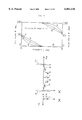
- FIG. 1 is a schematic cross-sectional view of a liquid crystal cell used in the liquid crystal display devices of the present invention.
- FIG. 2 is an explanatory view showing the structure of a liquid crystal display device of the present invention including the liquid crystal cell shown in FIG. 1.
- FIG. 3 is a graph and an explanatory drawing showing the change in orientation of liquid crystal molecules in a splay mode when a voltage was applied.
- FIG. 4 is a graph and an explanatory drawing showing the distribution of orientation of liquid crystal molecules in a bend mode.
- FIG. 5 is a graph and an explanatory drawing showing the distribution of orientation of liquid crystal molecules in a ⁇ -twist mode.
- FIG. 6 is an explanatory drawing showing the change in orientation of liquid crystal molecules in a splay mode when a voltage was applied.
- FIG. 7 is an explanatory drawing showing the fact that the orientation of liquid crystal molecules in a bend mode transforms into that of splay mode as applied voltage is increased.
- FIG. 8 is a graph showing the results of calculation of Gibbs free energy of liquid crystal molecules in three type of orientation modes.
- FIG. 9 is a graph showing the difference of free energy of liquid crystal molecules between a splay mode and other modes.
- FIG. 10 is a graph showing an example of dependency of V-T characteristic on wave length when an optical compensation plate is not used.
- FIG. 11 is an explanatory view showing the partial structure of a cell when optical compensation plate 11 was used.
- FIG. 12 is a graph showing an example of dependency of V-T characteristic on wave length when an optical compensation plate was used.
- FIG. 13 is a graph showing another example of dependency of V-T characteristic on wave length when an optical compensation plate was used.
- FIG. 14 is an explanatory drawing showing the definition of viewing angle used in the discussion of the characteristic of viewing angle.
- FIG. 15 is graphs showing examples of viewing angle characteristic when only an optical compensation plate was used.
- FIG. 16 is an explanatory drawing showing the partial structure of a cell when optical compensation plate 11 and optical compensation plate 13 were used.
- FIG. 17 is graphs showing examples of viewing angle characteristic when optical compensation plate 11 and optical compensation plate 13 were used.
- FIG. 18 is a graph showing an example of a response characteristic, at rise time, of a liquid crystal display device of the present invention.
- FIG. 19 is a graph showing an example of dependency of V-T characteristic on wave length in an example in which optical compensation plate 11 was used.
- FIG. 20 is a graph showing an example of a response characteristic at rise time in an example of the present invention.
- FIG. 21 is a graph showing an example of viewing angle characteristic in an example in which only optical compensation plate 11 was used.
- each of referential numerals 1 and 10 is a polarizer plate
- 11 is an optical compensation plate
- 2 and 9 are substrates
- 3 and 8 are transparent electrodes
- 4 and 7 are alignment films
- 5 is a liquid crystal
- 6 is a sealing material.
- FIG. 1 shows a diagrammatic cross-section of a liquid crystal cell used in the liquid crystal display devices of the present invention.
- transparent electrodes 3 and 8, and alignment films 4 and 7 are formed, in turn, on the inside surface of a pair of substrates 2 and 9 arranged facing with each other, respectively.
- liquid crystal 5 is filled by means of sealing material 6.
- a driving circuit for applying a voltage to the electrodes is provided.
- Two polarizer plates 1 and 10 are further provided so that they hold a pair of substrates 2 and 9 between them.
- optical compensation plate 11 is provided between substrate 2 and polarizer plate 1.
- 5A indicates a liquid crystal molecule.
- FIG. 2 is an explanatory drawing of a liquid crystal display device including a liquid crystal cell shown in FIG. 1.
- ⁇ 0 indicates a tilt angle from a substrate
- ⁇ 1 indicates an angle between the bearing angle (azimuth) of liquid crystal molecules and the transmission axis of a lower polarizer plate
- ⁇ 2 indicates an angle between the bearing angle of liquid crystal molecules and the transmission axis of an upper polarizer plate.
- liquid crystal 5 a nematic liquid crystal which is substantially free from a chiral liquid crystalline compound and has negative dielectric anisotropy is used as liquid crystal 5 (5A), liquid crystal molecule 5A placed between both substrates 2 and 9 is oriented so that its molecular axis is arranged on hypothetical plane 12 which is orthogonal to the substrate. In the vicinity of substrate 2 or 9, liquid crystal molecules are oriented vertically or semi-vertically so that the angle of the molecular axis is 90 to 45° and preferably 90 to 70° relative to the substrate.
- liquid crystal molecules are oriented so that the angle between the axis of liquid crystal molecules and the substrate becomes gradually smaller as the position of the molecule approaches to the center portion between both substrates, and the axis becomes parallel to the substrate at the center portion of the gap between both substrates. That is, liquid crystal molecules between upper substrate 2 and lower substrate 9 are arranged, without twist in orientation axis, on the same direction, namely, on hypothetical plane 12, in such a splayed way that liquid crystal molecule 5A at the center portion is oriented in substantially parallel to the substrate and the molecules are oriented in the direction of more vertical as the position of molecules approaches the substrate, as shown in FIG. 2. At both of the side where light enters and that where light exits, polarizers 10 and 1 are disposed, respectively.
- Angle ( ⁇ 1 ) of transmission axis of polarizer 10 at the side of light incidence is adjusted to 45° relative to the plane (XZ plane) of the bearing angle of liquid crystal molecules, and polarizer (analyzer) 1 at the side of light exiting is arranged so that the transmission axis of the polarizer 1 is orthogonal (at angle ⁇ 2 ) to that of the polarizer 10.
- polarizer 1 at the side of light exiting may be arranged in parallel to angle ⁇ 1 of polarizer 10 at the side of light incidence.
- substrate While glass substrates are generally used and transparent substrates of a plastic such as polycarbonate may be used, it is not limited to those substrates.
- Optical characteristic that is, light transmission T (V) of the cell can be expressed by the following equation when a medium having a uniaxial birefringence was placed under an orthogonal Nicol prism and a driving voltage was assumed to be V:
- d is cell thickness
- ⁇ n(V) is average value of optical anisotropy ⁇ n along the pass of light when driving voltage is V
- ⁇ is wave length of the light
- incident light is converted with a polarizer into straight-line polarized light.
- the condition of the incident light varies as it progresses through a liquid crystal layer. That is, it is possible to vary the conditions of polarization of light which passes through the liquid crystal, by changing the conditions of orientation of liquid crystal molecules by applying voltage. In other words, it is possible to vary light transmission by controlling average optical anisotropy of liquid crystal layer.
- the cell has a symmetrical structure relative to liquid crystal molecule 5A in the center portion, between right and left sides, and upper and lower sides, in the Figure, except for an optical compensation plate. That is, when X axis and y axis were assumed to be coordinate axes on a substrate, and Z axis was assumed to be a coordinate axis in the direction of cell thickness, liquid crystal molecules are oriented on the plane of X-Z axes, and thus viewing angle characteristic is symmetrical with respect to X-Z plane. In the same manner, since the cell is symmetrical between upper side and lower side relative to its center portion, viewing angle characteristic can be said to be symmetrical with respect to Y-Z axes. This fact means an improvement in the dependency on viewing angle which is a defect of conventional TN cells.
- pretilt angle ⁇ 0 of liquid crystal molecules in the vicinity of the surface of the substrate was decided as shown in FIG. 2, a plural number of orientation modes exist under the same substrate conditions.
- three type of orientation modes, splay, bend, and ⁇ -twist, which have a comparatively small Gibbs free energy appear.
- the conditions of orientation in a splay mode when the cell was observed from the direction of Y axis in the case where ⁇ 01 was adjusted to 80° and ⁇ 02 was adjusted to -80° is shown in FIG. 3, and the conditions of the orientation in a bend mode and ⁇ -twist mode are shown in FIGS. 4 and 5, respectively.
- z indicates the distance ( ⁇ m) in the direction of thickness in a liquid crystal cell
- ⁇ does a tilt angle (degree) of a liquid crystal molecule
- ⁇ does a twist angle (degree) of a liquid crystal molecule on a plane parallel to the substrate
- X does an axis at bearing angle of liquid crystal molecules parallel to the substrate
- Y does an axis parallel to the substrate and orthogonal to X axis
- Z does an axis orthogonal to the substrate and in the direction of cell thickness
- arrows a, b, c, d, and e indicate orientation vector of a liquid crystal molecule.
- FIG. 6 the state in which orientation in a splay mode varies when a voltage was applied is shown in FIG. 6.
- reference numerals 2 and 9 represent substrates
- V indicates a driving voltage
- Vc indicates critical voltage.
- orientation in a bend mode when voltage is applied is shown in FIG. 7.
- orientation becomes unstable in the vicinity of the substrate as voltage is gradually increased, and the orientation is transformed into a splay mode as a whole of the cell.
- twist modes of a righthanded rotation and a lefthanded rotation there exist twist modes of a righthanded rotation and a lefthanded rotation. Since the free energy of the righthanded and lefthanded rotation modes are equal when voltage is applied, either rotation may occur. In order to produce a righthanded rotation, it is sufficient to add a chiral agent in a concentration necessary to convert inherent twist into a righthanded rotation.
- GS represents free energy in a splay mode when a voltage is applied
- GB represents free energy in a bend mode when a voltage is applied
- GT represents free energy in a ⁇ twist mode when a voltage is applied. Difference in energy between the splay mode and bend mode, and between the splay mode and ⁇ twist mode are shown in FIG. 9.
- V-T characteristic was obtained in the case where it was assumed that optical anisotropy ⁇ n of a liquid crystal was 0.074, normal light refractive index n 0 was 1.491, pretilt angle ⁇ 01 was 75° and ⁇ 02 was -75°, cell thickness d was 15 ⁇ m, and polarizer plates were arranged at -45° and +45°, respectively, to the orientation plane of liquid crystal molecules. From FIG. 10, since the axis of abscissa indicates driving voltage V and the axis of ordinates indicates light transmission T, the curves are called V-T characteristic. V-T characteristic was obtained in the case where it was assumed that optical anisotropy ⁇ n of a liquid crystal was 0.074, normal light refractive index n 0 was 1.491, pretilt angle ⁇ 01 was 75° and ⁇ 02 was -75°, cell thickness d was 15 ⁇ m, and polarizer plates were arranged at -45° and +45°, respectively, to the orientation plane of
- FIG. 11 shows an example in which an optical compensation plate having a transversal retardation was inserted.
- refractive index of three main axes orthogonal with one another are Net, Not, and Not (Net>Not), and thus the plate is called uniaxially anisotropic phase difference plate.
- the angle of the axis showing an abnormal light refractive index Net relative to X-axis is ⁇ t, and thickness of optical compensation plate is dt.
- Transversal retardation Rt is expressed by the following equation:
- FIG. 12 shows the results of calculation on V-T characteristic when Rt was assumed to be 750 nm and ⁇ t was assumed to be 90° as an example. It can be seen that the dependency on wave length is reduced compared with the case of FIG. 10.
- FIG. 13 shows the results of calculation on V-T characteristic when Rt was assumed to be 1,000 nm and ⁇ t was assumed to be 90° as an example. V-T characteristic is reversed compared with the case of FIG. 12.
- V-T characteristic in FIG. 12 can be called normally black display, and V-T characteristic in FIG. 13 can be called normally white display.
- FIG. 15 Results of calculation on a viewing angle characteristic of cell shown in FIG. 11 according to the definition of viewing angle in the viewing angle characteristic shown in FIG. 14 is shown in FIG. 15.
- “Upper”, “Lower”, “Left”, and “Right” indicate viewing angles shown in FIG. 14, respectively
- V 1 ", “V 10 ", “V 50 “, “V 90 “, and “V 100” indicate the driving voltage at which voltage transmission becomes 1, 10, 50, 90, and 100%, respectively, when light was vertically entered.
- FIG. 15 shows the transmission when driving voltage is kept constant. From FIG. 15, it can be seen that viewing angle characteristic of liquid crystal display devices of the present invention have a good symmetry. However, it can be seen that the angle having a good visibility is about ⁇ 15° and thus it can not be said to be so wide.
- FIG. 16 shows an example in which optical compensation plate 13 having a longitudinal retardation was inserted in addition to optical compensation plate 11 having a transversal retardation.
- Optical compensation plate 13 can also be called uniaxially anisotropic phase difference plate, but refractive index of three main axes orthogonal with one another are Nol, Nol, and Nel (Nel>Nol), the axis which shows an abnormal light refractive index Nel is Z-axis, and thickness is dl.
- Longitudinal retardation Rl can be expressed by the following equation:
- FIG. 17 shows the results of calculation on viewing angle characteristic when an optical compensation plate 13 having an Rl of 1,000 nm was used together, and it can be seen that viewing angle characteristic is remarkably improved compared with the case of FIG. 15 and the angle of a good visibility becomes about ⁇ 500.
- a liquid crystal layer, optical compensation plate 11 having a transversal retardation, and optical compensation plate 13 having a longitudinal retardation are arranged so that light passes through them in that order.
- the method for arranging optical compensation plates is not limited to such order. For instance, it is possible to make it to the order of a liquid crystal layer, optical compensation plate 13, and then optical compensation plate 11. Also, an arrangement is possible in which the order of an optical compensation plate and a liquid crystal layer is changed so that light passes through a liquid crystal layer after it passes through an optical compensation plate. Further, it is possible to arrange them in the order of optical compensation plate 11 (or optical compensation plate 13), a liquid crystal layer, and optical compensation plate 13 (or optical compensation plate 11).
- optical compensation plates are symmetrically arranged before and behind a liquid crystal layer have the most excellent viewing angle characteristic. For example, it is best to arrange them in the order of optical compensation plate 13, optical compensation plate 11, a liquid crystal layer, optical compensation plate 11, and then optical compensation plate 13. However, it is desirable to adopt an arrangement as simple as possible from the view point of practical use.
- Biaxially anisotropic optical compensation plate means an optical compensation plate with which all of refractive index of three main axes n x , n y ,and n z , orthogonal with one another, are different. Further, it is possible to use another vertically arranged splayed nematic liquid crystal layer which is applied or not applied with a certain driving voltage, in place of an optical compensation plate, in addition to the liquid crystal layer shown in FIG. 16.
- FIG. 18 shows an example of the results of calculation on transmission-response characteristic of a liquid crystal display device of the present invention, and indicates that a space of time in which transmission reaches to 90% after a driving voltage is applied is about 16 msec. This is high speed compared with TN type liquid crystal display devices.
- the fact that the display devices of the present invention have a high response speed means that the devices are suitable for displaying high speed pictures such as TV pictures.
- Liquid crystal display devices described above are not driven as display device until the time when the orientation of liquid crystal molecules which are in a bend mode when driving voltage is 0 V is changed to a splay mode by the application of a driving voltage higher than critical voltage.
- it is permitted to fill, between substrates, a mixture of a liquid crystal with, for example, a monomer which is polymerizable by UV radiation, applying a driving voltage higher than critical voltage to orient the liquid crystal molecules in a splay mode, and then conducting a UV radiation under that state to polymerize the monomer thereby forming a network of a macromolecular compound in advance. If the devices were made once in such state beforehand, they can be driven as display device immediately after the application of a driving voltage.
- Liquid crystals used in the present invention exhibit a negative dielectric anisotropy, and are compositions composed of at least three components, and at least two kind of the components are compounds having a structural portion expressed by and selected from any one of formulas 1 to 5. Specifically, they are expressed by the following general formula (A).
- R 1 and R 2 are independent with each other, and represent an alkyl or alkenyl having up to 10 carbon atoms, and one or not adjacent two CH 2 groups in this formula may be replaced by --O--, --COO--, or --OCO--.
- B 1 , B 2 , and B 3 are independent with one another, and are 1,4-phenylene ring in which one or two CH groups in the ring may be replaced by nitrogen atom, phenylene ring substituted by fluorine atom, or 1,4-cyclohexylene ring;
- X 1 , X 2 , and X 3 are independent with one another, and --COO--, --OCO--, --OCH 2 --, --CH 2 O--, --CH 2 CH 2 --, --C.tbd.C--, or single bond;
- --A-- is a structural portion expressed by and selected from any one of formulas 1 to 5; and m and n are 0 or 1 provided that the total of l, m, and n is 1, 2, or 3.
- n-octadecyltriethoxy silane (ODS-E) material for vertical arrangement film, produced by Chisso Corporation) was spin-coated on a glass plate, and the surface of the coated film was subjected to a light rubbing treatment.
- the plate was used as substrate.
- Two substrates prepared by such method were used in combination in parallel arrangement as shown in FIGS. 1 and 2, and cell thickness was adjusted to 15 ⁇ m by inserting a sealing material.
- Liquid crystal of Composition Example 1 was filled as liquid crystal between the substrates to prepare a display device including a vertically arranged splayed nematic liquid crystal.
- Upper and lower polarizer plates were arranged to be -45° and ⁇ 45° relative to the plane of orientation of molecules, respectively.
- Results of measurement of V-T characteristic when light was vertically entered into the cell are shown in FIG. 19. The results were close to those shown in FIG. 12 which were theoretically forecasted.
- Results of measurement of transmission-response characteristic when a step-like driving voltage was applied to the cell is shown in FIG. 20. The results were close to those shown in FIG. 18 which were theoretically forecasted, and the speed of rising time was as fast as about 20 msec.
- Viewing angle characteristic when light was obliquely entered into the cell is shown in FIG. 21. The results were close to those shown in FIG. 15 which were theoretically forecasted.
- NI nematic-isotropic point (° C.)
- ⁇ does viscosity (mPa ⁇ sec)
- ⁇ n does optical anisotropy
- n 0 does normal light refractive index
- n e does abnormal light refractive index
- ⁇ does dielectric anisotropy
- ⁇ does dielectric constant in the direction of major axis
- ⁇ represents dielectric constant in the direction of minor axis.
- n-octadecyltriethoxy silane (ODS-E) material for vertical arrangement film, produced by Chisso Corporation) was spin-coated on a glass plate, and the surface of the coated film was subjected to a light rubbing treatment.
- the plate was used as substrate.
- Two substrates prepared by such method were used in combination in parallel arrangement as shown in FIGS. 1 and 2 to prepare a liquid crystal cell.
- Liquid crystal of the following Composition Example 2 was used as liquid crystal, and a display device including a vertically arranged splayed liquid crystal was prepared by the same manner as in Example 1 with the exception that upper and lower polarizer plates were arranged so that the upper polarizer was positioned at 90° relative to the lower polarizer. As the result, the same extent of good optical characteristic as in Example 1 was obtained.
- Display device including a vertically arranged splayed liquid crystal was prepared by the same manner as in Example 1 with the exception that liquid crystal of Composition Example 2 was used as liquid crystal, and upper and lower polarizer plates were arranged so that the upper polarizer was positioned at 90° relative to the lower polarizer. As the result, the same extent of good optical characteristic as in Example 1 was obtained.
- Liquid crystal of the following Composition Example 3 was filled as liquid crystal between the substrates to prepare a display device including a vertically arranged splayed liquid crystal.
- Liquid crystal of the following Composition Example 4 was filled as liquid crystal between the substrates to prepare a display device including a vertically arranged splayed liquid crystal.
- Upper and lower polarizer plates were arranged so that the upper polarizer was positioned at 90° relative to the lower polarizer, and the upper polarizer plate was arranged at 45° relative to the bearing angle of liquid crystal molecules. As the result, the same extent of good optical characteristic as in Example 1 was obtained.
- liquid crystal display devices having a wide viewing angle and a high response speed.
- liquid crystal display devices with which background is achromic and coloring is possible, and a high contrast, wide viewing angle, and high speed response can be actualized.
Abstract
In a liquid crystal display device including (1) a pair of substrates on the surface of which a transparent electrode and an alignment film are formed in turn, and the alignment films are arranged with a gap so that the films face each other, (2) a liquid crystal which fills the gap, (3) two polarizer plates holding the pair of substrates between them, and (4) a driving circuit connected to the transparent electrodes for applying a voltage between both substrates, the improved display device including a vertically arranged splayed nematic liquid crystal wherein a nematic liquid crystal which is substantially free from a chiral liquid crystalline compound and has a negative dielectric anisotropy is used as the liquid crystal; molecules of the liquid crystal between the pair of the substrates are oriented so that their molecular axis are arranged on planes orthogonal to the substrates; liquid crystal molecules, in the vicinity of the surface of the substrates, are oriented vertically or semi-vertically so that the angle between the axis of the molecules and the substrates is in the range of 90 to 45°; and liquid crystal molecules, in other portions, are oriented so that the angle between the axis of the molecules and the substrates becomes gradually smaller as the position of the molecules approaches the center portion of the gap between the substrates, and the axis becomes substantially parallel to the substrates in the center portion of the gap between the substrates.
Description
This application is a 371 of PCT/JP96/02785, filed Sep. 26, 1996.
The present invention relates to a liquid crystal display device. Particularly, it relates to a display device which includes a vertically arranged splayed nematic liquid crystal, and birefringence function of molecules of which liquid crystal can be controlled with voltage.
Heretofore, as the liquid crystal display device employing electrooptical effect, there have been developed many devices using a cell such as a DSM cell employing dynamic scattering effect, guest-host cell using a coloring matter, TN cell having a twisted nematic structure, SBE (Super-Twisted Birefringence Effect) cell, and STN (Super-Twisted Nematic) cell. Among these, most generally used liquid crystal display devices are based on Schadt, Helfrich effect using a nematic liquid crystal exhibiting positive dielectric anisotropy, and the liquid crystal has a twisted nematic structure. Recently, OCB (Optically Compensated Bend) cells having a wide viewing angle have been proposed as a mode which is close to practical use (Miyashita et al., Euro-Display '93 Digest, pp 149-152).
As display devices which use a liquid crystal material having negative dielectric anisotropy, ECB (Electrically Controlled Birefringence) type liquid crystal display devices employing electrically controlled birefringence effect are generally known. The devices are to employ the change in light transmission by effectively varying birefringence due to the deformation of a nematic layer having a negative dielectric anisotropy, in an electric field. The mode in which a new orientation control is added to the ECB mode and an optical compensation plate is used is a SH (Super-Homeotropic: Yamauchi et al., SID '89 Digest, pp 378-381) mode.
In these modes, display devices which use a liquid crystal material having positive dielectric anisotropy have a narrow viewing angle and an insufficient response speed. Also, ECB type liquid crystal display devices which employ negative dielectric anisotropy have such problems that response is slow, that steepness is poor, and that threshold voltage is high.
Whereas STN cell have recently come to be used for the first time as information terminals of personal computers and others, and it made actualization of large display devices of a highly definite picture possible, dependency on a viewing angle and an insufficient response speed are pointed out. In the case of large cells, also there is a problem in such an aspect of manufacturing process as grinding of glass substrates for obtaining uniform cell thickness. On the other hand, active matrix type cells in which a switch is provided for every picture segment are considered as prospective ones for display devices for future color personal computers, and have been remarkably improved in response speed. However, the problem is not yet sufficiently solved that they have a large dependency on a viewing angle which is peculiar to TN cells. As the mode in which dependency on viewing angle is improved, OCB (Optically Compensated Bend) cells are also proposed. However, OCB cells have problems that since orientation of liquid crystal molecules is initially splayed, it is necessary to initially apply a high voltage for a certain period of time to stably transform the splay orientation into bend orientation, and that the OCB cells have difficulties in orientation technique.
As the mode in which a liquid crystal material having negative dielectric anisotropy is used, the ECB type liquid crystal display devices described above and devices including a SH cell which employs an optical compensation plate are known. However, the former have problems that response speed is slow, that steepness is poor, and that voltage is high, and the latter have a problem that response speed is slow whereas monochromatic display is possible and dependency on viewing angle is improved.
The present invention is to cope with the problems in conventional technology, and thus one of its objects is to provide liquid crystal display devices background of which is achromatic and bright, and which are excellent in range of visibility, and with which a high contrast, a wide viewing angle, and high speed response are possible.
Aspects of the invention claimed in the present application are as follows:
(1) In a liquid crystal display device including
a pair of substrates on the surface of which a transparent electrode and an alignment film are formed in turn, and the alignment films are arranged with a gap so that the films face each other,
a liquid crystal which fills the gap,
two polarizer plates holding the pair of the substrates between them, and
a driving circuit connected to the transparent electrodes for applying a voltage between both substrates,
the improved display device including a vertically arranged splayed nematic liquid crystal wherein
a nematic liquid crystal which is substantially free from a chiral liquid crystalline compound and has a negative dielectric anisotropy is used as the liquid crystal,
liquid crystal molecules placed between the pair of the substrates are oriented so that their molecular axis are arranged on a plane orthogonal to the substrate, (or the plane on which liquid crystal molecules are splayed is arranged orthogonal in the substrate)
liquid crystal molecules, in the vicinity of the surface of the substrates, are oriented vertically or semi-vertically so that the angle between the axis of the molecules and the substrates is in the range of 90 to 45°, and
liquid crystal molecules, in other portions, are oriented so that the angle between the axis of the molecules and the substrates becomes gradually smaller as the position of the molecules approaches to the center portion of the gap between the substrates, and the axis becomes substantially parallel to the substrates in the center portion of the gap between the substrates.
(2) The display device including a vertically arranged splayed nematic liquid crystal recited in the aspect (1) described above wherein the transmission axis of one of polarizer plates is arranged in the direction of substantially 45° to the plane on which the axis of the liquid crystal molecules are arranged, and the transmission axis of the other of the polarizer plates is arranged substantially parallel or right angle to the transmission axis of the one of the polarizer plates.
(3) The display device including a vertically arranged splayed nematic liquid crystal recited in the aspect (1) or (2) described above wherein the liquid crystal is a composition of liquid crystalline compounds comprising at least three kind of components and having negative dielectric anisotropy, and at least two kind of the components are compounds having a structural portion expressed by and selected from any one of the following formulas 1 to 5. ##STR1## (4) The display device including a vertically arranged splayed nematic liquid crystal recited in any one of the aspects (1) to (3) described above wherein substrates on which a film of SiOx by an oblique evaporation, a film of a polymer, or film of a polysilane compound is formed at the side which faces the liquid crystal molecules, or substrates which were prepared by subjecting the film formed on the substrates defined just above to a rubbing treatment are used.
(5) The display device including a vertically arranged splayed nematic liquid crystal recited in any one of the aspects (1) to (4) described above wherein the device further includes optical compensating plate(s) having optical anisotropy and arranged between the polarizer plate and the substrate.
Liquid crystal display devices of the present invention are to control the birefringence function of liquid crystal molecule with voltage, and specifically, the devices are to employ the electrooptical effect described below. The present invention will be described in detail with reference to drawings.
FIG. 1 is a schematic cross-sectional view of a liquid crystal cell used in the liquid crystal display devices of the present invention.
FIG. 2 is an explanatory view showing the structure of a liquid crystal display device of the present invention including the liquid crystal cell shown in FIG. 1.
FIG. 3 is a graph and an explanatory drawing showing the change in orientation of liquid crystal molecules in a splay mode when a voltage was applied.
FIG. 4 is a graph and an explanatory drawing showing the distribution of orientation of liquid crystal molecules in a bend mode.
FIG. 5 is a graph and an explanatory drawing showing the distribution of orientation of liquid crystal molecules in a π-twist mode.
FIG. 6 is an explanatory drawing showing the change in orientation of liquid crystal molecules in a splay mode when a voltage was applied.
FIG. 7 is an explanatory drawing showing the fact that the orientation of liquid crystal molecules in a bend mode transforms into that of splay mode as applied voltage is increased.
FIG. 8 is a graph showing the results of calculation of Gibbs free energy of liquid crystal molecules in three type of orientation modes.
FIG. 9 is a graph showing the difference of free energy of liquid crystal molecules between a splay mode and other modes.
FIG. 10 is a graph showing an example of dependency of V-T characteristic on wave length when an optical compensation plate is not used.
FIG. 11 is an explanatory view showing the partial structure of a cell when optical compensation plate 11 was used.
FIG. 12 is a graph showing an example of dependency of V-T characteristic on wave length when an optical compensation plate was used.
FIG. 13 is a graph showing another example of dependency of V-T characteristic on wave length when an optical compensation plate was used.
FIG. 14 is an explanatory drawing showing the definition of viewing angle used in the discussion of the characteristic of viewing angle.
FIG. 15 is graphs showing examples of viewing angle characteristic when only an optical compensation plate was used.
FIG. 16 is an explanatory drawing showing the partial structure of a cell when optical compensation plate 11 and optical compensation plate 13 were used.
FIG. 17 is graphs showing examples of viewing angle characteristic when optical compensation plate 11 and optical compensation plate 13 were used.
FIG. 18 is a graph showing an example of a response characteristic, at rise time, of a liquid crystal display device of the present invention.
FIG. 19 is a graph showing an example of dependency of V-T characteristic on wave length in an example in which optical compensation plate 11 was used.
FIG. 20 is a graph showing an example of a response characteristic at rise time in an example of the present invention.
FIG. 21 is a graph showing an example of viewing angle characteristic in an example in which only optical compensation plate 11 was used.
In FIG. 1, each of referential numerals 1 and 10 is a polarizer plate, 11 is an optical compensation plate, 2 and 9 are substrates, 3 and 8 are transparent electrodes, 4 and 7 are alignment films, 5 is a liquid crystal, and 6 is a sealing material.
Specifically, FIG. 1 shows a diagrammatic cross-section of a liquid crystal cell used in the liquid crystal display devices of the present invention. In the Figure, transparent electrodes 3 and 8, and alignment films 4 and 7 are formed, in turn, on the inside surface of a pair of substrates 2 and 9 arranged facing with each other, respectively. Between the substrates, liquid crystal 5 is filled by means of sealing material 6. Between transparent electrodes 3 and 8, a driving circuit for applying a voltage to the electrodes is provided. Two polarizer plates 1 and 10 are further provided so that they hold a pair of substrates 2 and 9 between them. Also, optical compensation plate 11 is provided between substrate 2 and polarizer plate 1. In the Figure, 5A indicates a liquid crystal molecule.
FIG. 2 is an explanatory drawing of a liquid crystal display device including a liquid crystal cell shown in FIG. 1. In FIG. 2, θ0 indicates a tilt angle from a substrate, β1 indicates an angle between the bearing angle (azimuth) of liquid crystal molecules and the transmission axis of a lower polarizer plate, and β2 indicates an angle between the bearing angle of liquid crystal molecules and the transmission axis of an upper polarizer plate.
In the liquid crystal display device shown in FIG. 2, a nematic liquid crystal which is substantially free from a chiral liquid crystalline compound and has negative dielectric anisotropy is used as liquid crystal 5 (5A), liquid crystal molecule 5A placed between both substrates 2 and 9 is oriented so that its molecular axis is arranged on hypothetical plane 12 which is orthogonal to the substrate. In the vicinity of substrate 2 or 9, liquid crystal molecules are oriented vertically or semi-vertically so that the angle of the molecular axis is 90 to 45° and preferably 90 to 70° relative to the substrate. In other portions, liquid crystal molecules are oriented so that the angle between the axis of liquid crystal molecules and the substrate becomes gradually smaller as the position of the molecule approaches to the center portion between both substrates, and the axis becomes parallel to the substrate at the center portion of the gap between both substrates. That is, liquid crystal molecules between upper substrate 2 and lower substrate 9 are arranged, without twist in orientation axis, on the same direction, namely, on hypothetical plane 12, in such a splayed way that liquid crystal molecule 5A at the center portion is oriented in substantially parallel to the substrate and the molecules are oriented in the direction of more vertical as the position of molecules approaches the substrate, as shown in FIG. 2. At both of the side where light enters and that where light exits, polarizers 10 and 1 are disposed, respectively. Angle (β1) of transmission axis of polarizer 10 at the side of light incidence is adjusted to 45° relative to the plane (XZ plane) of the bearing angle of liquid crystal molecules, and polarizer (analyzer) 1 at the side of light exiting is arranged so that the transmission axis of the polarizer 1 is orthogonal (at angle β2) to that of the polarizer 10. However, polarizer 1 at the side of light exiting may be arranged in parallel to angle β1 of polarizer 10 at the side of light incidence.
As the method for attaining the vertical or semi-vertical orientation described above, a method which uses substrates on which SiOx is deposited by an oblique evaporation, or a polymer or a polysilane is coated; a method which uses substrates prepared by rubbing the surface of the deposited or coated film on those substrate; and a method which uses those methods in combination can be mentioned.
As substrate, while glass substrates are generally used and transparent substrates of a plastic such as polycarbonate may be used, it is not limited to those substrates.
Now, the principle of the present invention will be described with reference to FIGS. 1 and 2. In order to simplify the explanation, the case where an optical compensation plate is not used in FIGS. 1 and 2 is first discussed. Optical characteristic, that is, light transmission T (V) of the cell can be expressed by the following equation when a medium having a uniaxial birefringence was placed under an orthogonal Nicol prism and a driving voltage was assumed to be V:
T(V0=sin.sup.2 {πdΔn(V)/λ}×100(%)
wherein d is cell thickness, Δn(V) is average value of optical anisotropy Δn along the pass of light when driving voltage is V, and λ is wave length of the light.
In a qualitative discussion on light transmission, incident light is converted with a polarizer into straight-line polarized light. However, since the direction of the straight-line polarized light is different from the bearing angle of liquid crystal molecules, the condition of the incident light varies as it progresses through a liquid crystal layer. That is, it is possible to vary the conditions of polarization of light which passes through the liquid crystal, by changing the conditions of orientation of liquid crystal molecules by applying voltage. In other words, it is possible to vary light transmission by controlling average optical anisotropy of liquid crystal layer.
As will be understood from FIG. 2, the cell has a symmetrical structure relative to liquid crystal molecule 5A in the center portion, between right and left sides, and upper and lower sides, in the Figure, except for an optical compensation plate. That is, when X axis and y axis were assumed to be coordinate axes on a substrate, and Z axis was assumed to be a coordinate axis in the direction of cell thickness, liquid crystal molecules are oriented on the plane of X-Z axes, and thus viewing angle characteristic is symmetrical with respect to X-Z plane. In the same manner, since the cell is symmetrical between upper side and lower side relative to its center portion, viewing angle characteristic can be said to be symmetrical with respect to Y-Z axes. This fact means an improvement in the dependency on viewing angle which is a defect of conventional TN cells.
When pretilt angle θ0 of liquid crystal molecules in the vicinity of the surface of the substrate was decided as shown in FIG. 2, a plural number of orientation modes exist under the same substrate conditions. When voltage is not applied, three type of orientation modes, splay, bend, and π-twist, which have a comparatively small Gibbs free energy, appear. As an example, the conditions of orientation in a splay mode when the cell was observed from the direction of Y axis in the case where θ01 was adjusted to 80° and θ02 was adjusted to -80° is shown in FIG. 3, and the conditions of the orientation in a bend mode and π-twist mode are shown in FIGS. 4 and 5, respectively. In these Figures, z indicates the distance (μm) in the direction of thickness in a liquid crystal cell, θ does a tilt angle (degree) of a liquid crystal molecule, φ does a twist angle (degree) of a liquid crystal molecule on a plane parallel to the substrate, X does an axis at bearing angle of liquid crystal molecules parallel to the substrate, Y does an axis parallel to the substrate and orthogonal to X axis, Z does an axis orthogonal to the substrate and in the direction of cell thickness, and arrows a, b, c, d, and e indicate orientation vector of a liquid crystal molecule.
Next, the state in which orientation in a splay mode varies when a voltage was applied is shown in FIG. 6. In FIG. 6, reference numerals 2 and 9 represent substrates, V indicates a driving voltage, and Vc indicates critical voltage. When a voltage was applied on a liquid crystal material having a negative dielectric anisotropy and filled between substrates, a torque is applied on liquid crystal molecules to try to make the major axis of the molecules orient vertically to electric field, and almost all molecules except for those in the vicinity of the surface of the substrate are arranged parallel to the substrate.
The state of orientation in a bend mode when voltage is applied is shown in FIG. 7. In the bend mode, orientation becomes unstable in the vicinity of the substrate as voltage is gradually increased, and the orientation is transformed into a splay mode as a whole of the cell.
With respect to π-twist mode, there exist twist modes of a righthanded rotation and a lefthanded rotation. Since the free energy of the righthanded and lefthanded rotation modes are equal when voltage is applied, either rotation may occur. In order to produce a righthanded rotation, it is sufficient to add a chiral agent in a concentration necessary to convert inherent twist into a righthanded rotation.
These three type of orientations are decided by free energy within the cell. Then, the free energy in the cell was calculated by using Gibbs free energy. As examples, Gibbs free energy of each of the orientation modes was calculated on the assumption that dielectric anisotropy Δε of a liquid crystal is -5.4, dielectric constant in major direction ε∥ is 4.5, values of each of elastic constants, K11 is 8 pN, K22 is 6 pN, and K33 is 10 pN, twist angle is 0°, cell thickness is 10 μm, θ01 is 80°, and θ02 is -80° and the results are shown in FIG. 8. In FIG. 8, GS represents free energy in a splay mode when a voltage is applied, GB represents free energy in a bend mode when a voltage is applied, and GT represents free energy in a π twist mode when a voltage is applied. Difference in energy between the splay mode and bend mode, and between the splay mode and π twist mode are shown in FIG. 9.
From FIG. 9, it can be seen that when a voltage higher than a certain value is applied, the splay mode has the smallest energy among the three type of modes. This voltage is assumed to be critical voltage Vc. In the liquid crystal described above, it can be seen that since the voltage where the splay mode crosses with the bend mode is 1.727 V and the voltage where the splay mode crosses with the π twist mode is 1.773 V, the critical voltage is 1.773 V. Display devices of the present invention including a vertically arranged splayed nematic liquid crystal are driven at a voltage of root-mean-square value (effective value) higher than the critical voltage.
Results of calculation on electrooptical characteristic when a cell of the splay mode is used and polarizer plates are arranged at right angle are shown in FIG. 10. In FIG. 10, since the axis of abscissa indicates driving voltage V and the axis of ordinates indicates light transmission T, the curves are called V-T characteristic. V-T characteristic was obtained in the case where it was assumed that optical anisotropy Δn of a liquid crystal was 0.074, normal light refractive index n0 was 1.491, pretilt angle θ01 was 75° and θ02 was -75°, cell thickness d was 15 μm, and polarizer plates were arranged at -45° and +45°, respectively, to the orientation plane of liquid crystal molecules. From FIG. 10, it can be seen that when the wave length of light is varied from 467 nm to 633 nm, the V-T characteristic is varied largely dependent on the wave length of light. Accordingly, in this example, it has a fear of coloring at the time when voltage is applied. However, it is possible to reduce the dependency of V-T characteristic on wave length and to make it achromatic by using a uniaxial or biaxial optical compensation plate in combination as described below, and thus, monochrome display which is available also for color display is possible.
Next, the fact that the dependency of V-T characteristic on wave length can be reduced by means of an optical compensation plate having a transversal retardation is discussed. FIG. 11 shows an example in which an optical compensation plate having a transversal retardation was inserted. With respect to the optical compensation plate 11, refractive index of three main axes orthogonal with one another are Net, Not, and Not (Net>Not), and thus the plate is called uniaxially anisotropic phase difference plate. The angle of the axis showing an abnormal light refractive index Net relative to X-axis is φt, and thickness of optical compensation plate is dt. Transversal retardation Rt is expressed by the following equation:
Rt=(Net-Not)dt
It is possible to reduce the dependency of V-T characteristic on wave length by properly selecting the values of transversal retardation Rt and φt. FIG. 12 shows the results of calculation on V-T characteristic when Rt was assumed to be 750 nm and φt was assumed to be 90° as an example. It can be seen that the dependency on wave length is reduced compared with the case of FIG. 10. FIG. 13 shows the results of calculation on V-T characteristic when Rt was assumed to be 1,000 nm and φt was assumed to be 90° as an example. V-T characteristic is reversed compared with the case of FIG. 12. V-T characteristic in FIG. 12 can be called normally black display, and V-T characteristic in FIG. 13 can be called normally white display.
Results of calculation on a viewing angle characteristic of cell shown in FIG. 11 according to the definition of viewing angle in the viewing angle characteristic shown in FIG. 14 is shown in FIG. 15. In FIG. 15, "Upper", "Lower", "Left", and "Right" indicate viewing angles shown in FIG. 14, respectively, and "V1 ", "V10 ", "V50 ", "V90 ", and "V100 " indicate the driving voltage at which voltage transmission becomes 1, 10, 50, 90, and 100%, respectively, when light was vertically entered. Accordingly, FIG. 15 shows the transmission when driving voltage is kept constant. From FIG. 15, it can be seen that viewing angle characteristic of liquid crystal display devices of the present invention have a good symmetry. However, it can be seen that the angle having a good visibility is about ±15° and thus it can not be said to be so wide.
Next, the fact that in the liquid crystal display devices of the present invention, viewing angle characteristic can be expanded by using an optical compensation plate having a longitudinal retardation together is discussed. FIG. 16 shows an example in which optical compensation plate 13 having a longitudinal retardation was inserted in addition to optical compensation plate 11 having a transversal retardation. Optical compensation plate 13 can also be called uniaxially anisotropic phase difference plate, but refractive index of three main axes orthogonal with one another are Nol, Nol, and Nel (Nel>Nol), the axis which shows an abnormal light refractive index Nel is Z-axis, and thickness is dl. Longitudinal retardation Rl can be expressed by the following equation:
Rl=(Nel-Nol)dl
It is possible to expand the viewing angle characteristic by properly selecting the value of the longitudinal retardation Rl. FIG. 17 shows the results of calculation on viewing angle characteristic when an optical compensation plate 13 having an Rl of 1,000 nm was used together, and it can be seen that viewing angle characteristic is remarkably improved compared with the case of FIG. 15 and the angle of a good visibility becomes about ±500.
In the device shown in FIG. 16, a liquid crystal layer, optical compensation plate 11 having a transversal retardation, and optical compensation plate 13 having a longitudinal retardation are arranged so that light passes through them in that order. However, the method for arranging optical compensation plates is not limited to such order. For instance, it is possible to make it to the order of a liquid crystal layer, optical compensation plate 13, and then optical compensation plate 11. Also, an arrangement is possible in which the order of an optical compensation plate and a liquid crystal layer is changed so that light passes through a liquid crystal layer after it passes through an optical compensation plate. Further, it is possible to arrange them in the order of optical compensation plate 11 (or optical compensation plate 13), a liquid crystal layer, and optical compensation plate 13 (or optical compensation plate 11). Devices in which optical compensation plates are symmetrically arranged before and behind a liquid crystal layer have the most excellent viewing angle characteristic. For example, it is best to arrange them in the order of optical compensation plate 13, optical compensation plate 11, a liquid crystal layer, optical compensation plate 11, and then optical compensation plate 13. However, it is desirable to adopt an arrangement as simple as possible from the view point of practical use.
It is possible to use one biaxially anisotropic optical compensation plate in place of two uniaxially anisotropic optical compensation plates shown in FIG. 16. "Biaxially anisotropic optical compensation plate" means an optical compensation plate with which all of refractive index of three main axes nx, ny,and nz, orthogonal with one another, are different. Further, it is possible to use another vertically arranged splayed nematic liquid crystal layer which is applied or not applied with a certain driving voltage, in place of an optical compensation plate, in addition to the liquid crystal layer shown in FIG. 16.
Next, high speed response which is one of the characteristics of the liquid crystal display devices of the present invention is discussed. FIG. 18 shows an example of the results of calculation on transmission-response characteristic of a liquid crystal display device of the present invention, and indicates that a space of time in which transmission reaches to 90% after a driving voltage is applied is about 16 msec. This is high speed compared with TN type liquid crystal display devices. The fact that the display devices of the present invention have a high response speed means that the devices are suitable for displaying high speed pictures such as TV pictures.
Liquid crystal display devices described above are not driven as display device until the time when the orientation of liquid crystal molecules which are in a bend mode when driving voltage is 0 V is changed to a splay mode by the application of a driving voltage higher than critical voltage. In order to remove such inconvenience, it is permitted to fill, between substrates, a mixture of a liquid crystal with, for example, a monomer which is polymerizable by UV radiation, applying a driving voltage higher than critical voltage to orient the liquid crystal molecules in a splay mode, and then conducting a UV radiation under that state to polymerize the monomer thereby forming a network of a macromolecular compound in advance. If the devices were made once in such state beforehand, they can be driven as display device immediately after the application of a driving voltage.
Liquid crystals used in the present invention exhibit a negative dielectric anisotropy, and are compositions composed of at least three components, and at least two kind of the components are compounds having a structural portion expressed by and selected from any one of formulas 1 to 5. Specifically, they are expressed by the following general formula (A). General formula (A):
R.sup.1 -(B.sub.1 -X.sub.1)l-(B.sub.2 -X.sub.2).sub.m -A-(X.sub.3 -B.sub.3).sub.n -R.sup.2
wherein R1 and R2 are independent with each other, and represent an alkyl or alkenyl having up to 10 carbon atoms, and one or not adjacent two CH2 groups in this formula may be replaced by --O--, --COO--, or --OCO--. B1, B2, and B3 are independent with one another, and are 1,4-phenylene ring in which one or two CH groups in the ring may be replaced by nitrogen atom, phenylene ring substituted by fluorine atom, or 1,4-cyclohexylene ring; X1, X2, and X3 are independent with one another, and --COO--, --OCO--, --OCH2 --, --CH2 O--, --CH2 CH2 --, --C.tbd.C--, or single bond; --A-- is a structural portion expressed by and selected from any one of formulas 1 to 5; and m and n are 0 or 1 provided that the total of l, m, and n is 1, 2, or 3.
Examples of the preferable compounds are mentioned below. ##STR2##
Now, the present invention will be described in more detail with reference to Examples. However, the present invention is by no means restricted by these Examples.
In order to semi-vertically orient liquid crystal molecules in the vicinity of the surface of a glass substrate having a transparent electrode, n-octadecyltriethoxy silane ("ODS-E" material for vertical arrangement film, produced by Chisso Corporation) was spin-coated on a glass plate, and the surface of the coated film was subjected to a light rubbing treatment. The plate was used as substrate. Two substrates prepared by such method were used in combination in parallel arrangement as shown in FIGS. 1 and 2, and cell thickness was adjusted to 15μ m by inserting a sealing material. Liquid crystal of Composition Example 1 was filled as liquid crystal between the substrates to prepare a display device including a vertically arranged splayed nematic liquid crystal. Upper and lower polarizer plates were arranged to be -45° and ±45° relative to the plane of orientation of molecules, respectively. As optical compensation plate, only optical compensation plate 11 having a transversal retardation (Rt=750 nm) was used.
______________________________________
 ##STR3##                   20    Parts
 ##STR4##                   6
 ##STR5##                   5
 ##STR6##                   15
 ##STR7##                   9
 ##STR8##                   7
 ##STR9##                   8
 ##STR10##                  6
 ##STR11##                  6
 ##STR12##                  3
 ##STR13##                  3
 ##STR14##                  4
 ##STR15##                  3
 ##STR16##                  2
 ##STR17##                  4
 ##STR18##                  2
______________________________________
Results of measurement of V-T characteristic when light was vertically entered into the cell are shown in FIG. 19. The results were close to those shown in FIG. 12 which were theoretically forecasted. Results of measurement of transmission-response characteristic when a step-like driving voltage was applied to the cell is shown in FIG. 20. The results were close to those shown in FIG. 18 which were theoretically forecasted, and the speed of rising time was as fast as about 20 msec. Viewing angle characteristic when light was obliquely entered into the cell is shown in FIG. 21. The results were close to those shown in FIG. 15 which were theoretically forecasted.
Physical properties of liquid crystal of Composition Example 1 were as follows:
NI=63.3, η=39.4, Δn=0.074, n.sub.0 =1.491, n.sub.e =1.565, Δε=-5.4, ε∥=4.5, ε⊥=9.9
wherein NI represents nematic-isotropic point (° C.), η does viscosity (mPa·sec), Δn does optical anisotropy, n0 does normal light refractive index, ne does abnormal light refractive index, Δε does dielectric anisotropy, ε∥ does dielectric constant in the direction of major axis, and ε⊥ represents dielectric constant in the direction of minor axis.
In order to semi-vertically orient liquid crystal molecules in the vicinity of the surface of a glass substrate having a transparent electrode, n-octadecyltriethoxy silane ("ODS-E" material for vertical arrangement film, produced by Chisso Corporation) was spin-coated on a glass plate, and the surface of the coated film was subjected to a light rubbing treatment. The plate was used as substrate. Two substrates prepared by such method were used in combination in parallel arrangement as shown in FIGS. 1 and 2 to prepare a liquid crystal cell. Liquid crystal of the following Composition Example 2 was used as liquid crystal, and a display device including a vertically arranged splayed liquid crystal was prepared by the same manner as in Example 1 with the exception that upper and lower polarizer plates were arranged so that the upper polarizer was positioned at 90° relative to the lower polarizer. As the result, the same extent of good optical characteristic as in Example 1 was obtained.
______________________________________
 ##STR19##                  5     Parts
 ##STR20##                  6
 ##STR21##                  6
 ##STR22##                  7
 ##STR23##                  7
 ##STR24##                  12
 ##STR25##                  8
 ##STR26##                  4
 ##STR27##                  4
 ##STR28##                  4
 ##STR29##                  7
 ##STR30##                  6
 ##STR31##                  7
 ##STR32##                  2
 ##STR33##                  3
 ##STR34##                  4
 ##STR35##                  2
 ##STR36##                  2
 ##STR37##                  3
 ##STR38##                  2
______________________________________
Physical properties of liquid crystal of Composition Example 2 were as follows:
NI=57.4, η=47.0, Δn=0.137, n.sub.0 =1.655, n.sub.e =1.518, Δε=-2.7, ε∥=5.9, ε⊥=8.6
Display device including a vertically arranged splayed liquid crystal was prepared by the same manner as in Example 1 with the exception that liquid crystal of Composition Example 2 was used as liquid crystal, and upper and lower polarizer plates were arranged so that the upper polarizer was positioned at 90° relative to the lower polarizer. As the result, the same extent of good optical characteristic as in Example 1 was obtained.
In order to semi-vertically orient liquid crystal molecules in the vicinity of the surface of a glass substrate having a transparent electrode, SiOx was first deposited by oblique evaporation on a glass substrate and then n-octadecyltriethoxy silane ("ODS-E" material for vertical arrangement film, produced by Chisso Corporation) was spin-coated thereon. Two substrates prepared by such method were used in combination in parallel arrangement as shown in FIGS. 1 and 2 to prepare a liquid crystal cell. Liquid crystal of the following Composition Example 3 was filled as liquid crystal between the substrates to prepare a display device including a vertically arranged splayed liquid crystal. Upper and lower polarizer plates were arranged so that the upper polarizer was positioned at 90° relative to the lower polarizer, and the upper polarizer plate was arranged at 45° relative to the bearing angle of liquid crystal molecules. The liquid crystal display device had the same extent of good optical characteristic as that in Example 1.
______________________________________
 ##STR39##                  19    Parts
 ##STR40##                  19
 ##STR41##                  4
 ##STR42##                  4
 ##STR43##                  9
 ##STR44##                  7
 ##STR45##                  7
 ##STR46##                  6
 ##STR47##                  4
 ##STR48##                  5
 ##STR49##                  5
 ##STR50##                  10
______________________________________
Physical properties of liquid crystal of Composition Example 3 were as follows:
NI=70.6, η=24.4, Δn=0.0847, n.sub.0 =1.4847, n.sub.e =1.5694, Δε=-2.8, ε∥=3.8, ε⊥=6.6
In order to semi-vertically orient liquid crystal molecules in the vicinity of the surface of a glass substrate having a transparent electrode, SiOx was first deposited by oblique evaporation at 60° on a glass substrate and then it was further deposited by oblique evaporation at 85°. Two substrates prepared by such method were used in combination in parallel arrangement to prepare a liquid crystal cell. Liquid crystal of the following Composition Example 4 was filled as liquid crystal between the substrates to prepare a display device including a vertically arranged splayed liquid crystal. Upper and lower polarizer plates were arranged so that the upper polarizer was positioned at 90° relative to the lower polarizer, and the upper polarizer plate was arranged at 45° relative to the bearing angle of liquid crystal molecules. As the result, the same extent of good optical characteristic as in Example 1 was obtained.
______________________________________
 ##STR51##                  6     Parts
 ##STR52##                  4
 ##STR53##                  9
 ##STR54##                  5
 ##STR55##                  4
 ##STR56##                  9
 ##STR57##                  9
 ##STR58##                  8
 ##STR59##                  6
 ##STR60##                  10
 ##STR61##                  10
 ##STR62##                  10
 ##STR63##                  10
______________________________________
Physical properties of liquid crystal of Composition Example 4 were as follows:
NI=87.0, η=31.5, Δn=0.1225, n.sub.0 =1.4958, n.sub.e 1.6183, Δε=-1.4, ε∥=4.8, ε⊥=6.2
According to the Examples described above, it was possible to prepare liquid crystal display devices having a wide viewing angle and a high response speed.
In the Examples described above, it is possible to use one or two optical compensation plates or a vertically arranged splayed nematic liquid crystal cell between two polarizer plates as discussed above to facilitate the display excellent in visibility and having an achromatic background. Whereas examples in which polarizer plates were orthogonally arranged between upper and lower plates were demonstrated above, it may be parallel. Besides, arrangement of a polarizer plate is not restricted to 45° relative to the bearing angle of liquid crystal molecules. Further, whereas electrooptical measurement by transmission was carried out in the Examples described above, if a reflector plate was used in place of a polarizer plate arranged at one side, liquid crystal display devices of the present invention can achieve the same effect even as reflection type.
According to the present invention, it is possible to provide liquid crystal display devices with which background is achromic and coloring is possible, and a high contrast, wide viewing angle, and high speed response can be actualized.
Claims (9)
1. In a liquid crystal display device including
a pair of substrates on the surface of which a transparent electrode and an alignment film are formed in turn, and the alignment films are arranged with a gap so that the films face each other,
a liquid crystal which fills the gap,
two polarizer plates holding the pair of the substrates between them, and
a driving circuit connected to the transparent electrodes for applying a voltage between both substrates,
the improved display device including a vertically arranged splayed nematic liquid crystal wherein
a nematic liquid crystal which is substantially free from a chiral liquid crystalline compound and has a negative dielectric anisotropy is used as the liquid crystal,
liquid crystal molecules in the pair of the substrates are oriented so that their molecular axis are arranged on a plane orthogonal to the substrate,
liquid crystal molecules, in the vicinity of the surface of the substrates, are oriented vertically or semi-vertically so that the angle between the axis of the molecules and the substrates is in the range of 90 to 45°, and
liquid crystal molecules, in other portions, are oriented so that the angle between the axis of the molecules and the substrates becomes gradually smaller as the position of the molecules approaches to the center portion of the gap between the substrates, and the axis becomes substantially parallel to the substrates in the center portion of the gap between the substrates.
2. The display device including a vertically arranged splayed nematic liquid crystal according to claim 1 wherein the transmission axis of one of the polarizer plates is arranged in the direction of substantially 45° to the plane on which the axis of the liquid crystal molecules are arranged, and the transmission axis of the other of the polarizer plates is arranged substantially parallel or right angle to the transmission axis of the one of the polarizer plates.
3. The display device including a vertically arranged splayed nematic liquid crystal according to claim 1 or 2 wherein the liquid crystal is a composition of liquid crystalline compounds comprising at least three kind of components and having negative dielectric anisotropy, and at least two kind of the components are compounds having a structural portion expressed by and selected from any one of the following formulas 1 to 5. ##STR64##
4. The display device including a vertically arranged splayed nematic liquid crystal according to claim 1 or 2 wherein substrates on which a film of SiO2 by an oblique evaporation, a film of a polymer, or a coated film of a polysilane compound is formed at the side which faces the liquid crystal molecules, or substrates which were prepared by subjecting the film formed on the substrates defined above to a rubbing treatment are used.
5. The display device including a vertically arranged splayed nematic liquid crystal according to claim 1 or 2 wherein the device further includes optical compensating plate(s) having optical anisotropy and arranged between the polarizer plate and the substrate.
6. The display device including a vertically arranged splayed nematic liquid crystal according to claim 3 wherein substrates on which a film of SiO2 by an oblique evaporation, a film of a polymer, or a film of a polysilane compound is formed at the side which faces the liquid crystal molecules, or substrates which are prepared by subjecting the film formed on the substrates defined above to a rubbing treatment are used.
7. The display device including a vertically arranged splayed nematic liquid crystal according to claim 3 wherein the device further includes optical compensating plate(s) having optical anisotropy and arranged between the polarizer plate and the substrate.
8. The display device including a vertically arranged splayed nematic liquid crystal according to claim 4 wherein the device further includes optical compensating plate(s) having optical anisotropy and arranged between the polarizer plate and the substrate.
9. The display device including a vertically arranged splayed nematic liquid crystal according to claim 6 wherein the device further includes optical compensating plate(s) having optical anisotropy and arranged between the polarizer plate and the substrate.
Applications Claiming Priority (3)
| Application Number | Priority Date | Filing Date | Title |
|---|---|---|---|
| JP7-273562 | 1995-09-26 | ||
| JP27356295 | 1995-09-26 | ||
| PCT/JP1996/002785 WO1997012275A1 (en) | 1995-09-26 | 1996-09-26 | Homeotropic sprayed-nematic liquid crystal display device |
Publications (1)
| Publication Number | Publication Date |
|---|---|
| US6061116A true US6061116A (en) | 2000-05-09 |
Family
ID=17529541
Family Applications (1)
| Application Number | Title | Priority Date | Filing Date |
|---|---|---|---|
| US09/043,698 Expired - Fee Related US6061116A (en) | 1995-09-26 | 1996-09-26 | Homeotropic sprayed-nematic liquid crystal display device |
Country Status (4)
| Country | Link |
|---|---|
| US (1) | US6061116A (en) |
| EP (1) | EP0872757A4 (en) |
| AU (1) | AU7095996A (en) |
| WO (1) | WO1997012275A1 (en) |
Cited By (22)
| Publication number | Priority date | Publication date | Assignee | Title |
|---|---|---|---|---|
| US6339460B1 (en) * | 1998-07-15 | 2002-01-15 | International Business Machines Corp. | Liquid crystal display device |
| US6426786B1 (en) * | 1999-06-01 | 2002-07-30 | International Business Machines Corporation | Method of homeotropic alignment or tilted homeotropic alignment of liquid crystals by single oblique evaporation of oxides and liquid crystal display device formed thereby |
| US6452655B1 (en) * | 1997-01-24 | 2002-09-17 | Matsushita Electric Industrial Co., Ltd. | Liquid crystal device and its manufacturing method |
| US6469762B1 (en) * | 1999-06-29 | 2002-10-22 | Hyundai Display Technology Inc. | Optically compensated splay mode LCD |
| US6512561B1 (en) * | 1997-08-29 | 2003-01-28 | Sharp Kabushiki Kaisha | Liquid crystal display with at least one phase compensation element |
| US6542211B1 (en) * | 1998-06-18 | 2003-04-01 | Canon Kabushiki Kaisha | Liquid crystal device and driving method therefor |
| US6556267B2 (en) * | 1997-11-18 | 2003-04-29 | Sanyo Electric Co., Ltd. | Liquid crystal display and projector using the same |
| US6642981B1 (en) * | 1996-09-30 | 2003-11-04 | Fujitsu Display Technologies Corporation | Liquid crystal display device operating in a vertically aligned mode including at least one retardation film |
| US6671018B2 (en) * | 1999-12-27 | 2003-12-30 | Samsung Electronics Co., Ltd. | Liquid crystal display with only portion of the long axes of the liquid crystal molecules are arranged in radial configuration |
| US6781664B1 (en) * | 1999-07-22 | 2004-08-24 | Merck Patent Gmbh | Liquid-crystal switching elements comprising a liquid-crystal layer which has extremely low optical retardation and liquid-crystal displays containing them |
| US20040233356A1 (en) * | 2000-08-29 | 2004-11-25 | Nec Corporation | Method for producing a reflection liquid crystal display |
| US20040246388A1 (en) * | 2001-10-08 | 2004-12-09 | Lee Chang-Hun | Liquid crystal display and driving method thereof |
| US6903796B2 (en) * | 2000-07-07 | 2005-06-07 | Fujitsu Display Technologies Corporation | Liquid crystal display device using photo-cured product formed of photo-curing composition having liquid crystal skeletal structure and production method thereof |
| US20050140887A1 (en) * | 1998-05-16 | 2005-06-30 | Song Jang-Kun | Liquid crystal displays having multi-domains and a manufacturing method thereof |
| US20060072056A1 (en) * | 2004-10-05 | 2006-04-06 | Nec Lcd Technologies, Ltd. | LCD device reducing asymmetry in the leakage light |
| US20060114402A1 (en) * | 1997-05-29 | 2006-06-01 | Lyu Jae-Jin | Liquid crystal display having wide viewing angle |
| US7167224B1 (en) | 1997-06-12 | 2007-01-23 | Sharp Kabushiki Kaisha | Vertically-aligned (VA) liquid crystal display device |
| US20070081116A1 (en) * | 1999-10-01 | 2007-04-12 | Song Jang-Kun | Liquid crytsal display |
| US20070132928A1 (en) * | 2005-12-09 | 2007-06-14 | Innolux Display Corp. | Liquid crystal display having biaxial compensating film |
| US20090015772A1 (en) * | 2004-11-24 | 2009-01-15 | Kazutaka Hanaoka | Liquid crystal display device |
| CN101735823A (en) * | 2009-12-18 | 2010-06-16 | 北京八亿时空液晶材料科技有限公司 | Negative dielectric anisotropy liquid crystal composition |
| US20140098313A1 (en) * | 2012-10-08 | 2014-04-10 | Samsung Display Co., Ltd. | Liquid crystal display and method of manufacturing the same |
Families Citing this family (9)
| Publication number | Priority date | Publication date | Assignee | Title |
|---|---|---|---|---|
| GB2325056A (en) * | 1997-05-09 | 1998-11-11 | Sharp Kk | Polarisation independent optical phase modulator |
| EP0884619A3 (en) * | 1997-06-14 | 2000-04-19 | Sharp Kabushiki Kaisha | Plasma-addressed liquid crystal display device |
| US6221444B1 (en) * | 1998-06-10 | 2001-04-24 | Canon Kabushiki Kaisha | Liquid crystal device |
| JP2002182036A (en) | 2000-04-06 | 2002-06-26 | Fujitsu Ltd | Viewing angle compensation film and liquid crystal display device |
| JP4961151B2 (en) * | 2006-03-14 | 2012-06-27 | 株式会社リコー | Optical path deflecting element and image display device |
| JP2007286468A (en) * | 2006-04-19 | 2007-11-01 | Seiko Epson Corp | Method for manufacturing liquid crystal device |
| JP5169490B2 (en) * | 2008-05-28 | 2013-03-27 | セイコーエプソン株式会社 | Liquid crystal device, electronic device, and method of manufacturing liquid crystal device |
| CN107400519B (en) * | 2016-05-19 | 2021-02-19 | 北京八亿时空液晶科技股份有限公司 | Positive and negative mixed liquid crystal composition and application thereof |
| CN117586781A (en) | 2022-08-15 | 2024-02-23 | 捷恩智株式会社 | Liquid crystal composition, liquid crystal display element and application thereof |
Citations (4)
| Publication number | Priority date | Publication date | Assignee | Title |
|---|---|---|---|---|
| JPH02176625A (en) * | 1988-12-28 | 1990-07-09 | Fujitsu Ltd | Liquid crystal display device |
| JPH03209440A (en) * | 1990-01-12 | 1991-09-12 | Ricoh Co Ltd | Liquid crystal display element |
| JPH0682777A (en) * | 1992-09-07 | 1994-03-25 | Sumitomo Chem Co Ltd | Liquid crystal display device |
| US5621558A (en) * | 1994-04-20 | 1997-04-15 | Sharp Kabushiki Kaisha | Liquid crystal electro-optical device having alignment films for perpendicular alignment |
Family Cites Families (2)
| Publication number | Priority date | Publication date | Assignee | Title |
|---|---|---|---|---|
| JPS55127520A (en) * | 1979-03-26 | 1980-10-02 | Citizen Watch Co Ltd | Liquid crystal display element |
| JPH01209424A (en) * | 1988-02-17 | 1989-08-23 | Seiko Epson Corp | Liquid crystal electrooptic device |
-
1996
- 1996-09-26 US US09/043,698 patent/US6061116A/en not_active Expired - Fee Related
- 1996-09-26 EP EP96932001A patent/EP0872757A4/en not_active Withdrawn
- 1996-09-26 WO PCT/JP1996/002785 patent/WO1997012275A1/en not_active Application Discontinuation
- 1996-09-26 AU AU70959/96A patent/AU7095996A/en not_active Abandoned
Patent Citations (4)
| Publication number | Priority date | Publication date | Assignee | Title |
|---|---|---|---|---|
| JPH02176625A (en) * | 1988-12-28 | 1990-07-09 | Fujitsu Ltd | Liquid crystal display device |
| JPH03209440A (en) * | 1990-01-12 | 1991-09-12 | Ricoh Co Ltd | Liquid crystal display element |
| JPH0682777A (en) * | 1992-09-07 | 1994-03-25 | Sumitomo Chem Co Ltd | Liquid crystal display device |
| US5621558A (en) * | 1994-04-20 | 1997-04-15 | Sharp Kabushiki Kaisha | Liquid crystal electro-optical device having alignment films for perpendicular alignment |
Cited By (68)
| Publication number | Priority date | Publication date | Assignee | Title |
|---|---|---|---|---|
| US6642981B1 (en) * | 1996-09-30 | 2003-11-04 | Fujitsu Display Technologies Corporation | Liquid crystal display device operating in a vertically aligned mode including at least one retardation film |
| US7379140B2 (en) | 1996-09-30 | 2008-05-27 | Sharp Kabushiki Kaisha | Liquid crystal display device operating in a vertically aligned mode comprising an optically biaxial retardation film |
| US7075609B2 (en) | 1996-09-30 | 2006-07-11 | Sharp Kabushiki Kaisha | Liquid crystal display device comprising p-type liquid crystal layer operating in vertically aligned mode including first and second retardation films |
| US7995175B2 (en) | 1996-09-30 | 2011-08-09 | Sharp Kabushiki Kaisha | Liquid crystal display device |
| US20100277678A1 (en) * | 1996-09-30 | 2010-11-04 | Sharp Kabushiki Kaisha | Liquid crystal display device operating in a vertically aligned mode |
| US7808592B2 (en) | 1996-09-30 | 2010-10-05 | Sharp Kabushiki Kaisha | Liquid crystal display device operating in a vertical aligned mode having particular optical biaxial retardation film |
| US20060203150A1 (en) * | 1996-09-30 | 2006-09-14 | Katsufumi Ohmuro | Liquid crystaldisplay device operating in a vertically aligned mode |
| US7548294B2 (en) | 1996-09-30 | 2009-06-16 | Sharp Kabushiki Kaisha | Liquid crystal display device operating in a vertically aligned mode |
| US20050248704A1 (en) * | 1996-09-30 | 2005-11-10 | Fujitsu Display Technologies Corporation | Liquid crystal display device including first and second retardation films |
| US6452655B1 (en) * | 1997-01-24 | 2002-09-17 | Matsushita Electric Industrial Co., Ltd. | Liquid crystal device and its manufacturing method |
| US20080007665A1 (en) * | 1997-05-29 | 2008-01-10 | Samsung Electronics Co., Ltd | Liquid crystal display having wide viewing angle |
| US7768615B2 (en) | 1997-05-29 | 2010-08-03 | Samsung Electronics Co., Ltd. | Liquid crystal display having wide viewing angle |
| US9041891B2 (en) | 1997-05-29 | 2015-05-26 | Samsung Display Co., Ltd. | Liquid crystal display having wide viewing angle |
| US20060114402A1 (en) * | 1997-05-29 | 2006-06-01 | Lyu Jae-Jin | Liquid crystal display having wide viewing angle |
| US7304703B1 (en) | 1997-06-12 | 2007-12-04 | Sharp Kabushiki Kaisha | Vertically-aligned (VA) liquid crystal display device |
| US7821603B2 (en) | 1997-06-12 | 2010-10-26 | Sharp Kabushiki Kaisha | Vertically-alligned (VA) liquid crystal display device |
| US8553188B2 (en) | 1997-06-12 | 2013-10-08 | Sharp Kabushiki Kaisha | Liquid crystal display device |
| US8134671B2 (en) | 1997-06-12 | 2012-03-13 | Sharp Kabushiki Kaisha | Liquid crystal display device |
| USRE43123E1 (en) | 1997-06-12 | 2012-01-24 | Sharp Kabushiki Kaisha | Vertically-aligned (VA) liquid crystal display device |
| US20110176098A1 (en) * | 1997-06-12 | 2011-07-21 | Sharp Kabushiki Kaisha | Vertically-alligned (va) liquid crystal display device |
| US7965363B2 (en) | 1997-06-12 | 2011-06-21 | Sharp Kabushiki Kaisha | Vertically-aligned (VA) liquid crystal display device |
| US20080303997A1 (en) * | 1997-06-12 | 2008-12-11 | Sharp Kabushiki Kaisha | Vertically-alligned (va) liquid crystal display device |
| US7227606B2 (en) | 1997-06-12 | 2007-06-05 | Sharp Kabushiki Kaisha | Vertically-alligned (VA) liquid crystal display device |
| US20080165314A1 (en) * | 1997-06-12 | 2008-07-10 | Arihiro Takeda | Vertically-aligned (VA) liquid crystal display device |
| US7224421B1 (en) | 1997-06-12 | 2007-05-29 | Sharp Kabushiki Kaisha | Vertically-aligned (VA) liquid crystal display device |
| US7167224B1 (en) | 1997-06-12 | 2007-01-23 | Sharp Kabushiki Kaisha | Vertically-aligned (VA) liquid crystal display device |
| US20070064187A1 (en) * | 1997-06-12 | 2007-03-22 | Arihiro Takeda | Vertically-aligned (VA) liquid crystal display device |
| US7760305B2 (en) | 1997-06-12 | 2010-07-20 | Sharp Kabushiki Kaisha | Liquid crystal display device with multiple alignment structures |
| US20090207360A1 (en) * | 1997-06-12 | 2009-08-20 | Sharp Kabushiki Kaisha | Vertically-alligned (va) liquid crystal display device |
| US20030058393A1 (en) * | 1997-08-29 | 2003-03-27 | Sharp Kabushiki Kaisha | Liquid crystal display device |
| US7057689B2 (en) | 1997-08-29 | 2006-06-06 | Sharp Kabushiki Kaisha | Liquid crystal display with at least one phase compensation element |
| US6512561B1 (en) * | 1997-08-29 | 2003-01-28 | Sharp Kabushiki Kaisha | Liquid crystal display with at least one phase compensation element |
| US6556267B2 (en) * | 1997-11-18 | 2003-04-29 | Sanyo Electric Co., Ltd. | Liquid crystal display and projector using the same |
| US7570332B2 (en) | 1998-05-16 | 2009-08-04 | Samsung Electronics Co., Ltd. | Liquid crystal displays having multi-domains and a manufacturing method thereof |
| US7573554B2 (en) | 1998-05-16 | 2009-08-11 | Samsung Electronics Co., Ltd. | Liquid crystal displays having multi-domains and a manufacturing method thereof |
| US20080079886A1 (en) * | 1998-05-16 | 2008-04-03 | Samsung Electronics Co., Ltd | Liquid crystal displays having multi-domains and a manufacturing method thereof |
| US20050140887A1 (en) * | 1998-05-16 | 2005-06-30 | Song Jang-Kun | Liquid crystal displays having multi-domains and a manufacturing method thereof |
| US6693695B2 (en) * | 1998-06-18 | 2004-02-17 | Canon Kabushiki Kaisha | Liquid crystal device and driving method therefor |
| US6542211B1 (en) * | 1998-06-18 | 2003-04-01 | Canon Kabushiki Kaisha | Liquid crystal device and driving method therefor |
| US20030133065A1 (en) * | 1998-06-18 | 2003-07-17 | Shinjiro Okada | Liquid crystal device and driving method therefor |
| US6339460B1 (en) * | 1998-07-15 | 2002-01-15 | International Business Machines Corp. | Liquid crystal display device |
| US6426786B1 (en) * | 1999-06-01 | 2002-07-30 | International Business Machines Corporation | Method of homeotropic alignment or tilted homeotropic alignment of liquid crystals by single oblique evaporation of oxides and liquid crystal display device formed thereby |
| US6469762B1 (en) * | 1999-06-29 | 2002-10-22 | Hyundai Display Technology Inc. | Optically compensated splay mode LCD |
| US6781664B1 (en) * | 1999-07-22 | 2004-08-24 | Merck Patent Gmbh | Liquid-crystal switching elements comprising a liquid-crystal layer which has extremely low optical retardation and liquid-crystal displays containing them |
| US9557612B2 (en) | 1999-10-01 | 2017-01-31 | Samsung Display Co., Ltd. | Liquid crystal display |
| US8174651B2 (en) | 1999-10-01 | 2012-05-08 | Samsung Electronics Co., Ltd. | Liquid crystal display |
| US20100007834A1 (en) * | 1999-10-01 | 2010-01-14 | Song Jang-Kun | Liquid crystal display |
| US8817213B2 (en) | 1999-10-01 | 2014-08-26 | Samsung Display Co., Ltd. | Liquid crystal display |
| US8456597B2 (en) | 1999-10-01 | 2013-06-04 | Samsung Display Co., Ltd. | Liquid crystal display |
| US20070081116A1 (en) * | 1999-10-01 | 2007-04-12 | Song Jang-Kun | Liquid crytsal display |
| US7583345B2 (en) | 1999-10-01 | 2009-09-01 | Samsung Electronics Co., Ltd. | Liquid crystal display |
| US6671018B2 (en) * | 1999-12-27 | 2003-12-30 | Samsung Electronics Co., Ltd. | Liquid crystal display with only portion of the long axes of the liquid crystal molecules are arranged in radial configuration |
| US20040150774A1 (en) * | 1999-12-27 | 2004-08-05 | Lee Chang-Hun | Liquid crystal display |
| US6903796B2 (en) * | 2000-07-07 | 2005-06-07 | Fujitsu Display Technologies Corporation | Liquid crystal display device using photo-cured product formed of photo-curing composition having liquid crystal skeletal structure and production method thereof |
| US7006180B2 (en) * | 2000-08-29 | 2006-02-28 | Nec Corporation | Method for producing a reflection liquid crystal display |
| US20040233356A1 (en) * | 2000-08-29 | 2004-11-25 | Nec Corporation | Method for producing a reflection liquid crystal display |
| US20070132697A1 (en) * | 2001-10-08 | 2007-06-14 | Samsung Electronics Co., Ltd. | Liquid crystal display and driving method thereof |
| US20040246388A1 (en) * | 2001-10-08 | 2004-12-09 | Lee Chang-Hun | Liquid crystal display and driving method thereof |
| US7196686B2 (en) * | 2001-10-08 | 2007-03-27 | Samsung Electronics Co., Ltd. | Liquid crystal display and driving method thereof |
| US20060072056A1 (en) * | 2004-10-05 | 2006-04-06 | Nec Lcd Technologies, Ltd. | LCD device reducing asymmetry in the leakage light |
| US7532285B2 (en) * | 2004-10-05 | 2009-05-12 | Nec Lcd Technologies, Ltd. | LCD device reducing asymmetry in the leakage light |
| US8094278B2 (en) | 2004-11-24 | 2012-01-10 | Sharp Kabushiki Kaisha | Liquid crystal display device |
| US20090015772A1 (en) * | 2004-11-24 | 2009-01-15 | Kazutaka Hanaoka | Liquid crystal display device |
| US20070132928A1 (en) * | 2005-12-09 | 2007-06-14 | Innolux Display Corp. | Liquid crystal display having biaxial compensating film |
| CN101735823B (en) * | 2009-12-18 | 2014-04-02 | 北京八亿时空液晶科技股份有限公司 | Negative dielectric anisotropy liquid crystal composition |
| CN101735823A (en) * | 2009-12-18 | 2010-06-16 | 北京八亿时空液晶材料科技有限公司 | Negative dielectric anisotropy liquid crystal composition |
| US20140098313A1 (en) * | 2012-10-08 | 2014-04-10 | Samsung Display Co., Ltd. | Liquid crystal display and method of manufacturing the same |
| US9256103B2 (en) * | 2012-10-08 | 2016-02-09 | Samsung Display Co., Ltd. | Liquid crystal display including liquid crystal with different pretilt angles and method of manufacturing the same |
Also Published As
| Publication number | Publication date |
|---|---|
| AU7095996A (en) | 1997-04-17 |
| WO1997012275A1 (en) | 1997-04-03 |
| EP0872757A4 (en) | 1999-11-24 |
| EP0872757A1 (en) | 1998-10-21 |
Similar Documents
| Publication | Publication Date | Title |
|---|---|---|
| US6061116A (en) | Homeotropic sprayed-nematic liquid crystal display device | |
| KR100341296B1 (en) | Optical compaensator for super-twist nematic liquid crystal displays | |
| US7327432B2 (en) | Optically compensated electro-optical light modulation element with optically isotropic phase | |
| EP0768562B1 (en) | Liquid crystal device and method of making a liquid crystal device | |
| US5568294A (en) | Liquid crystal display device having a polymer functioning as an orientation layer and a retarder | |
| JPH02256021A (en) | Liquid crystal display device | |
| KR960007791B1 (en) | Electro-optical device | |
| US4815825A (en) | Liquid crystal display device | |
| EP0539991A1 (en) | Liquid crystal device and display apparatus | |
| Suh et al. | Novel electro‐optic effect associated with a homeotropic to twisted–planar transition in nematic liquid crystals | |
| JP2000292815A (en) | Perpendicularly aligned ecb mode liquid crystal display device | |
| US7758772B2 (en) | Composition comprising a liquid crystal material and an additive | |
| JPH0990434A (en) | Perpendicularly oriented twisted nematic liquid crystal display device | |
| Lee et al. | Chiral-doped optically compensated bend nematic liquid crystal cell with continuous deformation from twist to twisted bend state | |
| EP0283916B1 (en) | Liquid crystal light-modulating device imparted with memory effect and display unit utilizing same | |
| JP3830559B2 (en) | Optical compensation film and liquid crystal display device | |
| EP0566987A1 (en) | Ferroelectric liquid crystal displays | |
| JP3288697B2 (en) | Electro-optical system | |
| Lavrentovich et al. | Lyotropic chromonic liquid crystals for optical applications–an optical retardation plate for twisted nematic cells | |
| US6558759B2 (en) | Liquid crystal display device | |
| JP2921585B2 (en) | Liquid crystal display device | |
| JP3342940B2 (en) | Liquid crystal display | |
| EP0227419B1 (en) | Ferroelectric liquid crystal mixture and optical modulation element using same | |
| EP0393577B1 (en) | Liquid crystal composition and liquid crystal display using said composition | |
| Lee et al. | P‐93: High Performance 17.0 ″SVGA OCB Panel with Fast Initial Bend Transition |
Legal Events
| Date | Code | Title | Description |
|---|---|---|---|
| AS | Assignment |
Owner name: CHISSO CORPORATION, JAPAN Free format text: ASSIGNMENT OF ASSIGNORS INTEREST;ASSIGNORS:NISHIDA, SUSUMU;TAKAHASHI, HIROKI;SAITO, HIDEO;AND OTHERS;REEL/FRAME:009391/0966 Effective date: 19980413 |
|
| FEPP | Fee payment procedure |
Free format text: PAYOR NUMBER ASSIGNED (ORIGINAL EVENT CODE: ASPN); ENTITY STATUS OF PATENT OWNER: LARGE ENTITY |
|
| REMI | Maintenance fee reminder mailed | ||
| LAPS | Lapse for failure to pay maintenance fees | ||
| FP | Lapsed due to failure to pay maintenance fee |
Effective date: 20040509 |
|
| STCH | Information on status: patent discontinuation |
Free format text: PATENT EXPIRED DUE TO NONPAYMENT OF MAINTENANCE FEES UNDER 37 CFR 1.362 |