US6057596A - Chip carrier having a specific power join distribution structure - Google Patents
Chip carrier having a specific power join distribution structure Download PDFInfo
- Publication number
- US6057596A US6057596A US09/175,113 US17511398A US6057596A US 6057596 A US6057596 A US 6057596A US 17511398 A US17511398 A US 17511398A US 6057596 A US6057596 A US 6057596A
- Authority
- US
- United States
- Prior art keywords
- chip
- substrate
- joints
- balls
- chip carrier
- Prior art date
- Legal status (The legal status is an assumption and is not a legal conclusion. Google has not performed a legal analysis and makes no representation as to the accuracy of the status listed.)
- Expired - Lifetime
Links
Images


Classifications
-
- H—ELECTRICITY
- H01—ELECTRIC ELEMENTS
- H01L—SEMICONDUCTOR DEVICES NOT COVERED BY CLASS H10
- H01L23/00—Details of semiconductor or other solid state devices
- H01L23/48—Arrangements for conducting electric current to or from the solid state body in operation, e.g. leads, terminal arrangements ; Selection of materials therefor
- H01L23/50—Arrangements for conducting electric current to or from the solid state body in operation, e.g. leads, terminal arrangements ; Selection of materials therefor for integrated circuit devices, e.g. power bus, number of leads
-
- H—ELECTRICITY
- H01—ELECTRIC ELEMENTS
- H01L—SEMICONDUCTOR DEVICES NOT COVERED BY CLASS H10
- H01L23/00—Details of semiconductor or other solid state devices
- H01L23/48—Arrangements for conducting electric current to or from the solid state body in operation, e.g. leads, terminal arrangements ; Selection of materials therefor
- H01L23/488—Arrangements for conducting electric current to or from the solid state body in operation, e.g. leads, terminal arrangements ; Selection of materials therefor consisting of soldered or bonded constructions
- H01L23/498—Leads, i.e. metallisations or lead-frames on insulating substrates, e.g. chip carriers
- H01L23/49838—Geometry or layout
-
- H—ELECTRICITY
- H01—ELECTRIC ELEMENTS
- H01L—SEMICONDUCTOR DEVICES NOT COVERED BY CLASS H10
- H01L2924/00—Indexing scheme for arrangements or methods for connecting or disconnecting semiconductor or solid-state bodies as covered by H01L24/00
- H01L2924/0001—Technical content checked by a classifier
- H01L2924/0002—Not covered by any one of groups H01L24/00, H01L24/00 and H01L2224/00
-
- H—ELECTRICITY
- H01—ELECTRIC ELEMENTS
- H01L—SEMICONDUCTOR DEVICES NOT COVERED BY CLASS H10
- H01L2924/00—Indexing scheme for arrangements or methods for connecting or disconnecting semiconductor or solid-state bodies as covered by H01L24/00
- H01L2924/15—Details of package parts other than the semiconductor or other solid state devices to be connected
- H01L2924/151—Die mounting substrate
- H01L2924/153—Connection portion
- H01L2924/1531—Connection portion the connection portion being formed only on the surface of the substrate opposite to the die mounting surface
- H01L2924/15311—Connection portion the connection portion being formed only on the surface of the substrate opposite to the die mounting surface being a ball array, e.g. BGA
Definitions
- the present invention is related to a chip carrier, and especially to a chip carrier supporting multiple functions of high speed CPU and chip set.
- FIG. 1 is a sectional view of a conventional chip carrier with a ball grid array (BGA) substrate.
- BGA ball grid array
- a plurality of balls are disposed on the other side of the substrate 13.
- FIG. 2 shows one kind of the conventional chip carrier in which the grounded balls 21 are disposed on the central area of the substrate 24.
- the power balls 22 and the signal balls 23 indiscriminately surround outside the grounded ball 21 by a space.
- the conducting lines for connecting these balls to the chip on the first side of the substrate 24 are long and ineffective.
- the long conducting lines will cause a high resistance/inductance/capacitance (R/L/C) value which is very harmful to the transmission of signals.
- FIG. 3 shows another kind of the conventional chip carrier with a BGA substrate.
- the grounded balls 31 and the power balls 32 are disposed on the central area of one side of the substrate 34 and the signal balls 33 surround them. Both of the grounded balls 31 and the power balls 32 are disposed a on half of the central area right under the chip on the other side, respectively.
- the power balls 32 for energizing the chip are not workable under high temperature. This thermal effect may make the chip out of function.
- the grounded balls, power balls, and signal balls are located together, there is a big chance to make the different balls touch each other under improper treatment the chip carrier.
- An object of the present invention is to provide a chip carrier which can reduce the R/L/C value and increase the reliability.
- the chip carrier for carrying a chip includes a substrate having a first surface for mounting therein the chip wherein the substrate has a plurality of through holes and a plurality of conducting lines, a plurality of grounded joints set at a corresponding position of a second surface of the substrate under the chip and electrically connected to the chip by the plurality of conducting lines through the plurality of through holes for grounding, a plurality of signal joints surrounding the plurality of grounded joints on the second surface of the substrate and electrically connected to the chip by the plurality of conducting lines through the plurality of through holes for transmitting a series of signals, and a plurality of power joints set between the grounded joints and the signal joints and electrically connected to the chip by the plurality of conducting lines through the plurality of through holes for energizing the chip wherein there exists spaces among the ground joints, the signal joints and the power joints.
- the substrate further includes a power ring surrounding the chip on the first surface corresponding to the plurality of power joints set on the second surface of the substrate.
- the substrate is a ball grid array (BGA) substrate or a pin grid array (PGA) substrate.
- BGA ball grid array
- PGA pin grid array
- the grounded joints, the signal joints, and the power joints are grounded balls, signal balls, and power balls respectively.
- these three kinds of joints are grounded pins, signal pins, and power pins respectively.
- These three kinds of the balls have a specific ball pitch and the space between the grounded balls and the power balls has a width ranged from one to three times of the specific ball pitch.
- the specific ball pitch is 1.27 mm, 1.0 mm or less than 1.0 mm.
- the substrate is a two-layer substrate, a four-layer substrate or an even-layer substrate.
- FIG. 1 is a sectional view of a chip carrier with a ball grid array (BGA) substrate;
- BGA ball grid array
- FIG. 2 is a schematic diagram showing a conventional chip carrier with a BGA substrate
- FIG. 3 is a schematic diagram showing another conventional chip carrier with a BGA substrate
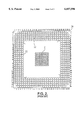
- FIG. 4 is a top view of a preferred embodiment of a chip carrier according to the present invention.
- FIG. 5 is a schematic diagram showing the preferred embodiment of a chip carrier with a BGA substrate according to the present invention.
- FIG. 4 is a top view of a chip carrier according to the present invention.
- a chip 4 is disposed on the center of the first side of the substrate of a chip carrier.
- the grounded ring 41 surrounds the chip 4 by a space and two power rings 42 surround the grounded ring 41 by another space.
- the rings are used for connecting the chip to the joints one the second side.
- the length of the conducting lines is an important factor which will influence the resistance/inductance/capacitance (R/L/C) value.
- FIG. 5 showing a preferred embodiment of a chip carrier according to the present invention.
- the grounded balls 51 are set in the central area of the second side of the chip carrier.
- the grounded balls 51 is right under the range within the grounded ring on the first side.
- the grounded balls 51 are connected with the grounded ring by the conducting lines through a plurality of through holes on the substrate.
- the power balls 52 surround with the grounded balls 51 by a specific space and are set right under the range within the two power rings on the first side.
- the power balls 52 are connected with the power rings by the conducting lines through a plurality of through holes on the substrate.
- the signal balls 53 surround outside the power balls 52 by another space.
- the space between the grounded balls 51 and the power balls 52 is ranged from one to three times of the ball pitch of balls and the ball pitch of the balls could be changed for different kinds of chips, depending on the package size.
- the ball pitchs of these three kinds of balls are 1.27 mm, 1.0 mm, or less than 1.0 mm.
- the power balls are not right under the chip so that the thermal effect cannot influence the power balls and the chip can have a better reliability. Besides, all of these balls right under their own rings can shorten the conducting line. Therefore, the R/L/C value can be minimized. By lowering the R/L/C value and shortening the length of conducting lines, the present invention can improve the reliability, and conducting efficiency of a chip.
- the preferred embodiment is a chip carrier with a BGA substrate
- the present invention can also be applied to a chip carrier with a pin grid array (PGA) substrate, depending on the applications of different joints.
- the substrate can also be a two-layer, a four-layer, or any even-layer substrate depending on the desired number of layers.
Abstract
Description
Claims (19)
Priority Applications (1)
| Application Number | Priority Date | Filing Date | Title |
|---|---|---|---|
| US09/175,113 US6057596A (en) | 1998-10-19 | 1998-10-19 | Chip carrier having a specific power join distribution structure |
Applications Claiming Priority (1)
| Application Number | Priority Date | Filing Date | Title |
|---|---|---|---|
| US09/175,113 US6057596A (en) | 1998-10-19 | 1998-10-19 | Chip carrier having a specific power join distribution structure |
Publications (1)
| Publication Number | Publication Date |
|---|---|
| US6057596A true US6057596A (en) | 2000-05-02 |
Family
ID=22638961
Family Applications (1)
| Application Number | Title | Priority Date | Filing Date |
|---|---|---|---|
| US09/175,113 Expired - Lifetime US6057596A (en) | 1998-10-19 | 1998-10-19 | Chip carrier having a specific power join distribution structure |
Country Status (1)
| Country | Link |
|---|---|
| US (1) | US6057596A (en) |
Cited By (27)
| Publication number | Priority date | Publication date | Assignee | Title |
|---|---|---|---|---|
| US6140710A (en) * | 1999-05-05 | 2000-10-31 | Lucent Technologies Inc. | Power and ground and signal layout for higher density integrated circuit connections with flip-chip bonding |
| US6297565B1 (en) * | 1998-03-31 | 2001-10-02 | Altera Corporation | Compatible IC packages and methods for ensuring migration path |
| US6384476B2 (en) * | 1999-04-19 | 2002-05-07 | Canon Kabushiki Kaisha | Semiconductor integrated circuit and printed wiring substrate provided with the same |
| US6403896B1 (en) | 2000-09-27 | 2002-06-11 | Advanced Semiconductor Engineering, Inc. | Substrate having specific pad distribution |
| US20020093079A1 (en) * | 2001-01-12 | 2002-07-18 | Wen-Yuan Chang | Grid array package with increased electrical grounding routes and method of fabrication |
| US6448639B1 (en) | 2000-09-18 | 2002-09-10 | Advanced Semiconductor Engineering, Inc. | Substrate having specific pad distribution |
| US6452262B1 (en) * | 2001-02-12 | 2002-09-17 | Lsi Logic Corporation | Layout of Vdd and Vss balls in a four layer PBGA |
| DE10109818A1 (en) * | 2001-03-01 | 2002-09-19 | Atmel Germany Gmbh | Semiconductor device has semiconductor body and associated carrier provided with flip-chip connections and furhter connections for dissipation of waste heat |
| WO2002080273A2 (en) * | 2001-03-30 | 2002-10-10 | Intel Corporation | Alternate bump metallurgy bars for power and ground routing |
| DE10121241A1 (en) * | 2001-04-30 | 2002-10-31 | Infineon Technologies Ag | Integrated circuit has high frequency signal connections arranged at center of package to minimize path lengths |
| US20020185308A1 (en) * | 2000-10-02 | 2002-12-12 | Cornelius William P. | Depopulation of a ball grid array to allow via placement |
| US6528872B2 (en) * | 2001-04-19 | 2003-03-04 | Via Technologies, Inc. | Packaging structure for ball grid array |
| US20030042619A1 (en) * | 2001-08-29 | 2003-03-06 | Via Technologies, Inc. | Configuration of conductive bumps and redistribution layer on a flip chip |
| US6734540B2 (en) * | 2000-10-11 | 2004-05-11 | Altera Corporation | Semiconductor package with stress inhibiting intermediate mounting substrate |
| US6744131B1 (en) * | 2003-04-22 | 2004-06-01 | Xilinx, Inc. | Flip chip integrated circuit packages accommodating exposed chip capacitors while providing structural rigidity |
| US20040212103A1 (en) * | 2000-06-19 | 2004-10-28 | Herman Kwong | Techniques for pin arrangements in circuit chips |
| US6930381B1 (en) * | 2002-04-12 | 2005-08-16 | Apple Computer, Inc. | Wire bonding method and apparatus for integrated circuit |
| US20050186769A1 (en) * | 2004-02-24 | 2005-08-25 | Young Dave W. | Hexagonal array structure for ball grid array packages |
| US7123480B1 (en) * | 1998-08-18 | 2006-10-17 | Oki Electric Industry Co., Ltd. | Package structure for a semiconductor device |
| CN1321452C (en) * | 2001-12-14 | 2007-06-13 | 威盛电子股份有限公司 | Grid matrix packed body for enhancing electric connected ground and packing method thereof |
| US20070152329A1 (en) * | 2005-12-29 | 2007-07-05 | Samsung Electronics Co., Ltd. | Heat-radiating semiconductor chip, tape wiring substrate and tape package using the same |
| US20070205018A1 (en) * | 2003-01-31 | 2007-09-06 | Hideki Koyama | Multilayer printed board, electronic apparatus, and packaging method |
| US20090310319A1 (en) * | 2004-12-17 | 2009-12-17 | Stmicroelectronics Sa. | Device for electrical connection of an integrated circuit chip |
| US7652361B1 (en) * | 2006-03-03 | 2010-01-26 | Amkor Technology, Inc. | Land patterns for a semiconductor stacking structure and method therefor |
| US20100078810A1 (en) * | 2008-09-30 | 2010-04-01 | Fujitsu Limited | Semiconductor apparatus, substrate design method, and substrate design apparatus |
| EP2135279A4 (en) * | 2007-04-03 | 2015-05-20 | Intel Corp | Polar hybrid grid array package |
| EP3916778A1 (en) * | 2015-08-31 | 2021-12-01 | Aisin Corporation | Semiconductor device, chip module, and semiconductor module |
Citations (5)
| Publication number | Priority date | Publication date | Assignee | Title |
|---|---|---|---|---|
| US4746966A (en) * | 1985-10-21 | 1988-05-24 | International Business Machines Corporation | Logic-circuit layout for large-scale integrated circuits |
| US5632631A (en) * | 1994-06-07 | 1997-05-27 | Tessera, Inc. | Microelectronic contacts with asperities and methods of making same |
| US5641988A (en) * | 1993-12-22 | 1997-06-24 | Vlsi Technology, Inc. | Multi-layered, integrated circuit package having reduced parasitic noise characteristics |
| US5796169A (en) * | 1996-11-19 | 1998-08-18 | International Business Machines Corporation | Structurally reinforced ball grid array semiconductor package and systems |
| US5895968A (en) * | 1993-10-22 | 1999-04-20 | Barber; Ivor | Semiconductor device assembly with minimized bond finger connections |
-
1998
- 1998-10-19 US US09/175,113 patent/US6057596A/en not_active Expired - Lifetime
Patent Citations (5)
| Publication number | Priority date | Publication date | Assignee | Title |
|---|---|---|---|---|
| US4746966A (en) * | 1985-10-21 | 1988-05-24 | International Business Machines Corporation | Logic-circuit layout for large-scale integrated circuits |
| US5895968A (en) * | 1993-10-22 | 1999-04-20 | Barber; Ivor | Semiconductor device assembly with minimized bond finger connections |
| US5641988A (en) * | 1993-12-22 | 1997-06-24 | Vlsi Technology, Inc. | Multi-layered, integrated circuit package having reduced parasitic noise characteristics |
| US5632631A (en) * | 1994-06-07 | 1997-05-27 | Tessera, Inc. | Microelectronic contacts with asperities and methods of making same |
| US5796169A (en) * | 1996-11-19 | 1998-08-18 | International Business Machines Corporation | Structurally reinforced ball grid array semiconductor package and systems |
Cited By (47)
| Publication number | Priority date | Publication date | Assignee | Title |
|---|---|---|---|---|
| US6423572B1 (en) | 1998-03-31 | 2002-07-23 | Altera Corporation | Compatible IC packages and methods for ensuring migration path |
| US6297565B1 (en) * | 1998-03-31 | 2001-10-02 | Altera Corporation | Compatible IC packages and methods for ensuring migration path |
| US7514768B2 (en) * | 1998-08-18 | 2009-04-07 | Oki Electric Industry Co., Ltd. | Package structure for a semiconductor device incorporating enhanced solder bump structure |
| US7123480B1 (en) * | 1998-08-18 | 2006-10-17 | Oki Electric Industry Co., Ltd. | Package structure for a semiconductor device |
| US20070008704A1 (en) * | 1998-08-18 | 2007-01-11 | Oki Electric Industry Co., Ltd. | Package structure for a semiconductor device |
| US6384476B2 (en) * | 1999-04-19 | 2002-05-07 | Canon Kabushiki Kaisha | Semiconductor integrated circuit and printed wiring substrate provided with the same |
| US6140710A (en) * | 1999-05-05 | 2000-10-31 | Lucent Technologies Inc. | Power and ground and signal layout for higher density integrated circuit connections with flip-chip bonding |
| US20040212103A1 (en) * | 2000-06-19 | 2004-10-28 | Herman Kwong | Techniques for pin arrangements in circuit chips |
| US6448639B1 (en) | 2000-09-18 | 2002-09-10 | Advanced Semiconductor Engineering, Inc. | Substrate having specific pad distribution |
| US6403896B1 (en) | 2000-09-27 | 2002-06-11 | Advanced Semiconductor Engineering, Inc. | Substrate having specific pad distribution |
| US7279356B2 (en) | 2000-10-02 | 2007-10-09 | Apple Inc. | Depopulation of a ball grid array to allow via placement |
| US20020185308A1 (en) * | 2000-10-02 | 2002-12-12 | Cornelius William P. | Depopulation of a ball grid array to allow via placement |
| US7112880B2 (en) * | 2000-10-02 | 2006-09-26 | Apple Computer, Inc. | Depopulation of a ball grid array to allow via placement |
| US20070072342A1 (en) * | 2000-10-02 | 2007-03-29 | Cornelius William P | Depopulation of a ball grid array to allow via placement |
| US6834427B2 (en) * | 2000-10-02 | 2004-12-28 | Apple Computer, Inc. | Method for depopulating of a ball grid array to allow via placement |
| US6734540B2 (en) * | 2000-10-11 | 2004-05-11 | Altera Corporation | Semiconductor package with stress inhibiting intermediate mounting substrate |
| US20020093079A1 (en) * | 2001-01-12 | 2002-07-18 | Wen-Yuan Chang | Grid array package with increased electrical grounding routes and method of fabrication |
| US6452262B1 (en) * | 2001-02-12 | 2002-09-17 | Lsi Logic Corporation | Layout of Vdd and Vss balls in a four layer PBGA |
| DE10109818A1 (en) * | 2001-03-01 | 2002-09-19 | Atmel Germany Gmbh | Semiconductor device has semiconductor body and associated carrier provided with flip-chip connections and furhter connections for dissipation of waste heat |
| WO2002080273A3 (en) * | 2001-03-30 | 2003-07-03 | Intel Corp | Alternate bump metallurgy bars for power and ground routing |
| US6653563B2 (en) | 2001-03-30 | 2003-11-25 | Intel Corporation | Alternate bump metallurgy bars for power and ground routing |
| WO2002080273A2 (en) * | 2001-03-30 | 2002-10-10 | Intel Corporation | Alternate bump metallurgy bars for power and ground routing |
| US6528872B2 (en) * | 2001-04-19 | 2003-03-04 | Via Technologies, Inc. | Packaging structure for ball grid array |
| US6911732B2 (en) | 2001-04-30 | 2005-06-28 | Infineon Technologies Ag | Integrated circuit |
| DE10121241A1 (en) * | 2001-04-30 | 2002-10-31 | Infineon Technologies Ag | Integrated circuit has high frequency signal connections arranged at center of package to minimize path lengths |
| DE10121241B4 (en) * | 2001-04-30 | 2005-07-07 | Infineon Technologies Ag | Integrated circuit |
| US20040145036A1 (en) * | 2001-04-30 | 2004-07-29 | Simon Muff | Integrated circuit |
| US6777815B2 (en) * | 2001-08-29 | 2004-08-17 | Via Technologies, Inc. | Configuration of conductive bumps and redistribution layer on a flip chip |
| US20030042619A1 (en) * | 2001-08-29 | 2003-03-06 | Via Technologies, Inc. | Configuration of conductive bumps and redistribution layer on a flip chip |
| CN1321452C (en) * | 2001-12-14 | 2007-06-13 | 威盛电子股份有限公司 | Grid matrix packed body for enhancing electric connected ground and packing method thereof |
| US6930381B1 (en) * | 2002-04-12 | 2005-08-16 | Apple Computer, Inc. | Wire bonding method and apparatus for integrated circuit |
| US20050263793A1 (en) * | 2002-04-12 | 2005-12-01 | Cornelius William P | Wire bonding method and apparatus for integrated circuit |
| US7298040B2 (en) * | 2002-04-12 | 2007-11-20 | Apple Inc. | Wire bonding method and apparatus for integrated circuit |
| US20070205018A1 (en) * | 2003-01-31 | 2007-09-06 | Hideki Koyama | Multilayer printed board, electronic apparatus, and packaging method |
| US6744131B1 (en) * | 2003-04-22 | 2004-06-01 | Xilinx, Inc. | Flip chip integrated circuit packages accommodating exposed chip capacitors while providing structural rigidity |
| US7259453B2 (en) * | 2004-02-24 | 2007-08-21 | Intel Corporation | Hexagonal array structure for ball grid array packages |
| US20050186769A1 (en) * | 2004-02-24 | 2005-08-25 | Young Dave W. | Hexagonal array structure for ball grid array packages |
| US20090310319A1 (en) * | 2004-12-17 | 2009-12-17 | Stmicroelectronics Sa. | Device for electrical connection of an integrated circuit chip |
| US7888791B2 (en) * | 2004-12-17 | 2011-02-15 | Stmicroelectronics S.A. | Device for electrical connection of an integrated circuit chip |
| CN1992247B (en) * | 2005-12-29 | 2012-03-14 | 三星电子株式会社 | Heat-radiating semiconductor chip, tape wiring substrate and tape package using the same |
| US7589421B2 (en) * | 2005-12-29 | 2009-09-15 | Samsung Electronics Co., Ltd. | Heat-radiating semiconductor chip, tape wiring substrate and tape package using the same |
| US20070152329A1 (en) * | 2005-12-29 | 2007-07-05 | Samsung Electronics Co., Ltd. | Heat-radiating semiconductor chip, tape wiring substrate and tape package using the same |
| US7652361B1 (en) * | 2006-03-03 | 2010-01-26 | Amkor Technology, Inc. | Land patterns for a semiconductor stacking structure and method therefor |
| EP2135279A4 (en) * | 2007-04-03 | 2015-05-20 | Intel Corp | Polar hybrid grid array package |
| US20100078810A1 (en) * | 2008-09-30 | 2010-04-01 | Fujitsu Limited | Semiconductor apparatus, substrate design method, and substrate design apparatus |
| US8816510B2 (en) * | 2008-09-30 | 2014-08-26 | Fujitsu Limited | Semiconductor apparatus, substrate design method, and substrate design apparatus |
| EP3916778A1 (en) * | 2015-08-31 | 2021-12-01 | Aisin Corporation | Semiconductor device, chip module, and semiconductor module |
Similar Documents
| Publication | Publication Date | Title |
|---|---|---|
| US6057596A (en) | Chip carrier having a specific power join distribution structure | |
| US20040188856A1 (en) | [flip-chip die and flip-chip package substrate] | |
| US6046909A (en) | Computer card with a printed circuit board with vias providing strength to the printed circuit board | |
| US5686764A (en) | Flip chip package with reduced number of package layers | |
| US5825628A (en) | Electronic package with enhanced pad design | |
| US7543377B2 (en) | Perimeter matrix ball grid array circuit package with a populated center | |
| US6323116B1 (en) | Differential pair geometry for integrated circuit chip packages | |
| KR970030718A (en) | Pad and Through Hole Arrangements for Semiconductor Packages | |
| CN102165584A (en) | Input/output architecture for mounted processors, and methods of using same | |
| US7095107B2 (en) | Ball assignment schemes for integrated circuit packages | |
| JP2001024084A (en) | Area array type semiconductor device | |
| US5703402A (en) | Output mapping of die pad bonds in a ball grid array | |
| US6664620B2 (en) | Integrated circuit die and/or package having a variable pitch contact array for maximization of number of signal lines per routing layer | |
| US5650660A (en) | Circuit pattern for a ball grid array integrated circuit package | |
| US6452262B1 (en) | Layout of Vdd and Vss balls in a four layer PBGA | |
| US6774498B2 (en) | Flip-chip package substrate | |
| US6601225B2 (en) | Semiconductor device having definite size of input/output blocks and its designing method | |
| US6740965B2 (en) | Flip-chip package substrate | |
| KR100329952B1 (en) | Semiconductor integrated circuit and wiring method thereof | |
| US20030227093A1 (en) | Flip-chip package substrate and flip chip die | |
| CN112151506B (en) | Electronic packaging structure and chip thereof | |
| US5365406A (en) | Master-slice type semiconductor integrated circuit device | |
| US7655872B2 (en) | Through-hole arrangement for a ball grid array package | |
| JPH1197613A (en) | Ic package | |
| US6515362B2 (en) | Grid array package with increased electrical grounding routes and method of fabrication |
Legal Events
| Date | Code | Title | Description |
|---|---|---|---|
| AS | Assignment |
Owner name: SILICON INTEGRATED SYSTEMS CORP., TAIWAN Free format text: ASSIGNMENT OF ASSIGNORS INTEREST;ASSIGNORS:LIN, WEI-FENG;HO, TONY H.;REEL/FRAME:009533/0214;SIGNING DATES FROM 19980926 TO 19981009 |
|
| STCF | Information on status: patent grant |
Free format text: PATENTED CASE |
|
| FEPP | Fee payment procedure |
Free format text: PAT HOLDER NO LONGER CLAIMS SMALL ENTITY STATUS, ENTITY STATUS SET TO UNDISCOUNTED (ORIGINAL EVENT CODE: STOL); ENTITY STATUS OF PATENT OWNER: LARGE ENTITY |
|
| FEPP | Fee payment procedure |
Free format text: ENTITY STATUS SET TO UNDISCOUNTED (ORIGINAL EVENT CODE: BIG.); ENTITY STATUS OF PATENT OWNER: LARGE ENTITY |
|
| FPAY | Fee payment |
Year of fee payment: 4 |
|
| FPAY | Fee payment |
Year of fee payment: 8 |
|
| FPAY | Fee payment |
Year of fee payment: 12 |