US6050481A - Method of making a high melting point solder ball coated with a low melting point solder - Google Patents
Method of making a high melting point solder ball coated with a low melting point solder Download PDFInfo
- Publication number
- US6050481A US6050481A US08/882,459 US88245997A US6050481A US 6050481 A US6050481 A US 6050481A US 88245997 A US88245997 A US 88245997A US 6050481 A US6050481 A US 6050481A
- Authority
- US
- United States
- Prior art keywords
- solder
- solder ball
- melting point
- paste
- mils
- Prior art date
- Legal status (The legal status is an assumption and is not a legal conclusion. Google has not performed a legal analysis and makes no representation as to the accuracy of the status listed.)
- Expired - Lifetime
Links
Images


Classifications
-
- H—ELECTRICITY
- H05—ELECTRIC TECHNIQUES NOT OTHERWISE PROVIDED FOR
- H05K—PRINTED CIRCUITS; CASINGS OR CONSTRUCTIONAL DETAILS OF ELECTRIC APPARATUS; MANUFACTURE OF ASSEMBLAGES OF ELECTRICAL COMPONENTS
- H05K3/00—Apparatus or processes for manufacturing printed circuits
- H05K3/30—Assembling printed circuits with electric components, e.g. with resistor
- H05K3/32—Assembling printed circuits with electric components, e.g. with resistor electrically connecting electric components or wires to printed circuits
- H05K3/34—Assembling printed circuits with electric components, e.g. with resistor electrically connecting electric components or wires to printed circuits by soldering
- H05K3/341—Surface mounted components
- H05K3/3431—Leadless components
- H05K3/3436—Leadless components having an array of bottom contacts, e.g. pad grid array or ball grid array components
-
- B—PERFORMING OPERATIONS; TRANSPORTING
- B23—MACHINE TOOLS; METAL-WORKING NOT OTHERWISE PROVIDED FOR
- B23K—SOLDERING OR UNSOLDERING; WELDING; CLADDING OR PLATING BY SOLDERING OR WELDING; CUTTING BY APPLYING HEAT LOCALLY, e.g. FLAME CUTTING; WORKING BY LASER BEAM
- B23K3/00—Tools, devices, or special appurtenances for soldering, e.g. brazing, or unsoldering, not specially adapted for particular methods
- B23K3/06—Solder feeding devices; Solder melting pans
- B23K3/0607—Solder feeding devices
- B23K3/0623—Solder feeding devices for shaped solder piece feeding, e.g. preforms, bumps, balls, pellets, droplets
-
- H—ELECTRICITY
- H01—ELECTRIC ELEMENTS
- H01L—SEMICONDUCTOR DEVICES NOT COVERED BY CLASS H10
- H01L21/00—Processes or apparatus adapted for the manufacture or treatment of semiconductor or solid state devices or of parts thereof
- H01L21/02—Manufacture or treatment of semiconductor devices or of parts thereof
- H01L21/04—Manufacture or treatment of semiconductor devices or of parts thereof the devices having at least one potential-jump barrier or surface barrier, e.g. PN junction, depletion layer or carrier concentration layer
- H01L21/48—Manufacture or treatment of parts, e.g. containers, prior to assembly of the devices, using processes not provided for in a single one of the subgroups H01L21/06 - H01L21/326
- H01L21/4814—Conductive parts
- H01L21/4846—Leads on or in insulating or insulated substrates, e.g. metallisation
- H01L21/4853—Connection or disconnection of other leads to or from a metallisation, e.g. pins, wires, bumps
-
- H—ELECTRICITY
- H01—ELECTRIC ELEMENTS
- H01L—SEMICONDUCTOR DEVICES NOT COVERED BY CLASS H10
- H01L24/00—Arrangements for connecting or disconnecting semiconductor or solid-state bodies; Methods or apparatus related thereto
- H01L24/01—Means for bonding being attached to, or being formed on, the surface to be connected, e.g. chip-to-package, die-attach, "first-level" interconnects; Manufacturing methods related thereto
- H01L24/10—Bump connectors ; Manufacturing methods related thereto
- H01L24/11—Manufacturing methods
-
- B—PERFORMING OPERATIONS; TRANSPORTING
- B23—MACHINE TOOLS; METAL-WORKING NOT OTHERWISE PROVIDED FOR
- B23K—SOLDERING OR UNSOLDERING; WELDING; CLADDING OR PLATING BY SOLDERING OR WELDING; CUTTING BY APPLYING HEAT LOCALLY, e.g. FLAME CUTTING; WORKING BY LASER BEAM
- B23K2101/00—Articles made by soldering, welding or cutting
- B23K2101/36—Electric or electronic devices
-
- H—ELECTRICITY
- H01—ELECTRIC ELEMENTS
- H01L—SEMICONDUCTOR DEVICES NOT COVERED BY CLASS H10
- H01L2224/00—Indexing scheme for arrangements for connecting or disconnecting semiconductor or solid-state bodies and methods related thereto as covered by H01L24/00
- H01L2224/01—Means for bonding being attached to, or being formed on, the surface to be connected, e.g. chip-to-package, die-attach, "first-level" interconnects; Manufacturing methods related thereto
- H01L2224/02—Bonding areas; Manufacturing methods related thereto
- H01L2224/04—Structure, shape, material or disposition of the bonding areas prior to the connecting process
- H01L2224/05—Structure, shape, material or disposition of the bonding areas prior to the connecting process of an individual bonding area
- H01L2224/0554—External layer
- H01L2224/0556—Disposition
- H01L2224/05568—Disposition the whole external layer protruding from the surface
-
- H—ELECTRICITY
- H01—ELECTRIC ELEMENTS
- H01L—SEMICONDUCTOR DEVICES NOT COVERED BY CLASS H10
- H01L2224/00—Indexing scheme for arrangements for connecting or disconnecting semiconductor or solid-state bodies and methods related thereto as covered by H01L24/00
- H01L2224/01—Means for bonding being attached to, or being formed on, the surface to be connected, e.g. chip-to-package, die-attach, "first-level" interconnects; Manufacturing methods related thereto
- H01L2224/02—Bonding areas; Manufacturing methods related thereto
- H01L2224/04—Structure, shape, material or disposition of the bonding areas prior to the connecting process
- H01L2224/05—Structure, shape, material or disposition of the bonding areas prior to the connecting process of an individual bonding area
- H01L2224/0554—External layer
- H01L2224/05573—Single external layer
-
- H—ELECTRICITY
- H01—ELECTRIC ELEMENTS
- H01L—SEMICONDUCTOR DEVICES NOT COVERED BY CLASS H10
- H01L2224/00—Indexing scheme for arrangements for connecting or disconnecting semiconductor or solid-state bodies and methods related thereto as covered by H01L24/00
- H01L2224/01—Means for bonding being attached to, or being formed on, the surface to be connected, e.g. chip-to-package, die-attach, "first-level" interconnects; Manufacturing methods related thereto
- H01L2224/02—Bonding areas; Manufacturing methods related thereto
- H01L2224/04—Structure, shape, material or disposition of the bonding areas prior to the connecting process
- H01L2224/05—Structure, shape, material or disposition of the bonding areas prior to the connecting process of an individual bonding area
- H01L2224/0554—External layer
- H01L2224/05599—Material
- H01L2224/056—Material with a principal constituent of the material being a metal or a metalloid, e.g. boron [B], silicon [Si], germanium [Ge], arsenic [As], antimony [Sb], tellurium [Te] and polonium [Po], and alloys thereof
-
- H—ELECTRICITY
- H01—ELECTRIC ELEMENTS
- H01L—SEMICONDUCTOR DEVICES NOT COVERED BY CLASS H10
- H01L2224/00—Indexing scheme for arrangements for connecting or disconnecting semiconductor or solid-state bodies and methods related thereto as covered by H01L24/00
- H01L2224/01—Means for bonding being attached to, or being formed on, the surface to be connected, e.g. chip-to-package, die-attach, "first-level" interconnects; Manufacturing methods related thereto
- H01L2224/10—Bump connectors; Manufacturing methods related thereto
- H01L2224/11—Manufacturing methods
- H01L2224/113—Manufacturing methods by local deposition of the material of the bump connector
- H01L2224/1133—Manufacturing methods by local deposition of the material of the bump connector in solid form
- H01L2224/11334—Manufacturing methods by local deposition of the material of the bump connector in solid form using preformed bumps
-
- H—ELECTRICITY
- H01—ELECTRIC ELEMENTS
- H01L—SEMICONDUCTOR DEVICES NOT COVERED BY CLASS H10
- H01L2224/00—Indexing scheme for arrangements for connecting or disconnecting semiconductor or solid-state bodies and methods related thereto as covered by H01L24/00
- H01L2224/01—Means for bonding being attached to, or being formed on, the surface to be connected, e.g. chip-to-package, die-attach, "first-level" interconnects; Manufacturing methods related thereto
- H01L2224/10—Bump connectors; Manufacturing methods related thereto
- H01L2224/12—Structure, shape, material or disposition of the bump connectors prior to the connecting process
- H01L2224/13—Structure, shape, material or disposition of the bump connectors prior to the connecting process of an individual bump connector
- H01L2224/13001—Core members of the bump connector
- H01L2224/13099—Material
-
- H—ELECTRICITY
- H01—ELECTRIC ELEMENTS
- H01L—SEMICONDUCTOR DEVICES NOT COVERED BY CLASS H10
- H01L2224/00—Indexing scheme for arrangements for connecting or disconnecting semiconductor or solid-state bodies and methods related thereto as covered by H01L24/00
- H01L2224/80—Methods for connecting semiconductor or other solid state bodies using means for bonding being attached to, or being formed on, the surface to be connected
- H01L2224/81—Methods for connecting semiconductor or other solid state bodies using means for bonding being attached to, or being formed on, the surface to be connected using a bump connector
- H01L2224/8112—Aligning
- H01L2224/81136—Aligning involving guiding structures, e.g. spacers or supporting members
- H01L2224/81138—Aligning involving guiding structures, e.g. spacers or supporting members the guiding structures being at least partially left in the finished device
-
- H—ELECTRICITY
- H01—ELECTRIC ELEMENTS
- H01L—SEMICONDUCTOR DEVICES NOT COVERED BY CLASS H10
- H01L24/00—Arrangements for connecting or disconnecting semiconductor or solid-state bodies; Methods or apparatus related thereto
- H01L24/01—Means for bonding being attached to, or being formed on, the surface to be connected, e.g. chip-to-package, die-attach, "first-level" interconnects; Manufacturing methods related thereto
- H01L24/02—Bonding areas ; Manufacturing methods related thereto
- H01L24/04—Structure, shape, material or disposition of the bonding areas prior to the connecting process
- H01L24/05—Structure, shape, material or disposition of the bonding areas prior to the connecting process of an individual bonding area
-
- H—ELECTRICITY
- H01—ELECTRIC ELEMENTS
- H01L—SEMICONDUCTOR DEVICES NOT COVERED BY CLASS H10
- H01L2924/00—Indexing scheme for arrangements or methods for connecting or disconnecting semiconductor or solid-state bodies as covered by H01L24/00
- H01L2924/01—Chemical elements
- H01L2924/01005—Boron [B]
-
- H—ELECTRICITY
- H01—ELECTRIC ELEMENTS
- H01L—SEMICONDUCTOR DEVICES NOT COVERED BY CLASS H10
- H01L2924/00—Indexing scheme for arrangements or methods for connecting or disconnecting semiconductor or solid-state bodies as covered by H01L24/00
- H01L2924/01—Chemical elements
- H01L2924/01006—Carbon [C]
-
- H—ELECTRICITY
- H01—ELECTRIC ELEMENTS
- H01L—SEMICONDUCTOR DEVICES NOT COVERED BY CLASS H10
- H01L2924/00—Indexing scheme for arrangements or methods for connecting or disconnecting semiconductor or solid-state bodies as covered by H01L24/00
- H01L2924/01—Chemical elements
- H01L2924/01013—Aluminum [Al]
-
- H—ELECTRICITY
- H01—ELECTRIC ELEMENTS
- H01L—SEMICONDUCTOR DEVICES NOT COVERED BY CLASS H10
- H01L2924/00—Indexing scheme for arrangements or methods for connecting or disconnecting semiconductor or solid-state bodies as covered by H01L24/00
- H01L2924/01—Chemical elements
- H01L2924/01015—Phosphorus [P]
-
- H—ELECTRICITY
- H01—ELECTRIC ELEMENTS
- H01L—SEMICONDUCTOR DEVICES NOT COVERED BY CLASS H10
- H01L2924/00—Indexing scheme for arrangements or methods for connecting or disconnecting semiconductor or solid-state bodies as covered by H01L24/00
- H01L2924/01—Chemical elements
- H01L2924/01029—Copper [Cu]
-
- H—ELECTRICITY
- H01—ELECTRIC ELEMENTS
- H01L—SEMICONDUCTOR DEVICES NOT COVERED BY CLASS H10
- H01L2924/00—Indexing scheme for arrangements or methods for connecting or disconnecting semiconductor or solid-state bodies as covered by H01L24/00
- H01L2924/01—Chemical elements
- H01L2924/01033—Arsenic [As]
-
- H—ELECTRICITY
- H01—ELECTRIC ELEMENTS
- H01L—SEMICONDUCTOR DEVICES NOT COVERED BY CLASS H10
- H01L2924/00—Indexing scheme for arrangements or methods for connecting or disconnecting semiconductor or solid-state bodies as covered by H01L24/00
- H01L2924/01—Chemical elements
- H01L2924/01076—Osmium [Os]
-
- H—ELECTRICITY
- H01—ELECTRIC ELEMENTS
- H01L—SEMICONDUCTOR DEVICES NOT COVERED BY CLASS H10
- H01L2924/00—Indexing scheme for arrangements or methods for connecting or disconnecting semiconductor or solid-state bodies as covered by H01L24/00
- H01L2924/01—Chemical elements
- H01L2924/01082—Lead [Pb]
-
- H—ELECTRICITY
- H01—ELECTRIC ELEMENTS
- H01L—SEMICONDUCTOR DEVICES NOT COVERED BY CLASS H10
- H01L2924/00—Indexing scheme for arrangements or methods for connecting or disconnecting semiconductor or solid-state bodies as covered by H01L24/00
- H01L2924/013—Alloys
- H01L2924/0132—Binary Alloys
- H01L2924/01322—Eutectic Alloys, i.e. obtained by a liquid transforming into two solid phases
-
- H—ELECTRICITY
- H01—ELECTRIC ELEMENTS
- H01L—SEMICONDUCTOR DEVICES NOT COVERED BY CLASS H10
- H01L2924/00—Indexing scheme for arrangements or methods for connecting or disconnecting semiconductor or solid-state bodies as covered by H01L24/00
- H01L2924/013—Alloys
- H01L2924/014—Solder alloys
-
- H—ELECTRICITY
- H01—ELECTRIC ELEMENTS
- H01L—SEMICONDUCTOR DEVICES NOT COVERED BY CLASS H10
- H01L2924/00—Indexing scheme for arrangements or methods for connecting or disconnecting semiconductor or solid-state bodies as covered by H01L24/00
- H01L2924/10—Details of semiconductor or other solid state devices to be connected
- H01L2924/11—Device type
- H01L2924/12—Passive devices, e.g. 2 terminal devices
- H01L2924/1204—Optical Diode
- H01L2924/12042—LASER
-
- H—ELECTRICITY
- H01—ELECTRIC ELEMENTS
- H01L—SEMICONDUCTOR DEVICES NOT COVERED BY CLASS H10
- H01L2924/00—Indexing scheme for arrangements or methods for connecting or disconnecting semiconductor or solid-state bodies as covered by H01L24/00
- H01L2924/10—Details of semiconductor or other solid state devices to be connected
- H01L2924/11—Device type
- H01L2924/14—Integrated circuits
-
- H—ELECTRICITY
- H01—ELECTRIC ELEMENTS
- H01L—SEMICONDUCTOR DEVICES NOT COVERED BY CLASS H10
- H01L2924/00—Indexing scheme for arrangements or methods for connecting or disconnecting semiconductor or solid-state bodies as covered by H01L24/00
- H01L2924/30—Technical effects
- H01L2924/35—Mechanical effects
- H01L2924/351—Thermal stress
- H01L2924/3511—Warping
-
- H—ELECTRICITY
- H05—ELECTRIC TECHNIQUES NOT OTHERWISE PROVIDED FOR
- H05K—PRINTED CIRCUITS; CASINGS OR CONSTRUCTIONAL DETAILS OF ELECTRIC APPARATUS; MANUFACTURE OF ASSEMBLAGES OF ELECTRICAL COMPONENTS
- H05K2201/00—Indexing scheme relating to printed circuits covered by H05K1/00
- H05K2201/10—Details of components or other objects attached to or integrated in a printed circuit board
- H05K2201/10613—Details of electrical connections of non-printed components, e.g. special leads
- H05K2201/10954—Other details of electrical connections
- H05K2201/10992—Using different connection materials, e.g. different solders, for the same connection
-
- H—ELECTRICITY
- H05—ELECTRIC TECHNIQUES NOT OTHERWISE PROVIDED FOR
- H05K—PRINTED CIRCUITS; CASINGS OR CONSTRUCTIONAL DETAILS OF ELECTRIC APPARATUS; MANUFACTURE OF ASSEMBLAGES OF ELECTRICAL COMPONENTS
- H05K2203/00—Indexing scheme relating to apparatus or processes for manufacturing printed circuits covered by H05K3/00
- H05K2203/03—Metal processing
- H05K2203/0338—Transferring metal or conductive material other than a circuit pattern, e.g. bump, solder, printed component
-
- H—ELECTRICITY
- H05—ELECTRIC TECHNIQUES NOT OTHERWISE PROVIDED FOR
- H05K—PRINTED CIRCUITS; CASINGS OR CONSTRUCTIONAL DETAILS OF ELECTRIC APPARATUS; MANUFACTURE OF ASSEMBLAGES OF ELECTRICAL COMPONENTS
- H05K2203/00—Indexing scheme relating to apparatus or processes for manufacturing printed circuits covered by H05K3/00
- H05K2203/04—Soldering or other types of metallurgic bonding
- H05K2203/041—Solder preforms in the shape of solder balls
-
- H—ELECTRICITY
- H05—ELECTRIC TECHNIQUES NOT OTHERWISE PROVIDED FOR
- H05K—PRINTED CIRCUITS; CASINGS OR CONSTRUCTIONAL DETAILS OF ELECTRIC APPARATUS; MANUFACTURE OF ASSEMBLAGES OF ELECTRICAL COMPONENTS
- H05K3/00—Apparatus or processes for manufacturing printed circuits
- H05K3/30—Assembling printed circuits with electric components, e.g. with resistor
- H05K3/32—Assembling printed circuits with electric components, e.g. with resistor electrically connecting electric components or wires to printed circuits
- H05K3/34—Assembling printed circuits with electric components, e.g. with resistor electrically connecting electric components or wires to printed circuits by soldering
- H05K3/3457—Solder materials or compositions; Methods of application thereof
- H05K3/3485—Applying solder paste, slurry or powder
-
- Y—GENERAL TAGGING OF NEW TECHNOLOGICAL DEVELOPMENTS; GENERAL TAGGING OF CROSS-SECTIONAL TECHNOLOGIES SPANNING OVER SEVERAL SECTIONS OF THE IPC; TECHNICAL SUBJECTS COVERED BY FORMER USPC CROSS-REFERENCE ART COLLECTIONS [XRACs] AND DIGESTS
- Y02—TECHNOLOGIES OR APPLICATIONS FOR MITIGATION OR ADAPTATION AGAINST CLIMATE CHANGE
- Y02P—CLIMATE CHANGE MITIGATION TECHNOLOGIES IN THE PRODUCTION OR PROCESSING OF GOODS
- Y02P70/00—Climate change mitigation technologies in the production process for final industrial or consumer products
- Y02P70/50—Manufacturing or production processes characterised by the final manufactured product
Definitions
- This invention is related to the field of semiconductor packaging. More specifically, the invention relates to a method for creating solder balls that provide a reliable electrical and mechanical connection between a first object containing solder ball structures and a second object.
- solder balls are superior to pins in all of the above features as well as being surface mountable, which has obvious implications given the increasingly small dimensions in the forefront technologies today.
- solder mounting is hardly a new technology, itself. But, the need remains to improve the solder systems and configurations in electronic structures.
- the use of solder ball connectors has been applied to the mounting of integrated circuit chips using the C-4 (controlled collapse chip connection) technology since the method and structure were first described and patented in U.S. Pat. Nos. 3,401,126 and 3,429,040 to Miller et al., which are assigned to the present assignee.
- a myriad of solder structures have since been proposed for the mounting of IC chips, as well as for interconnection of other levels of circuitry and associated electronic packaging.
- solder structures have been proposed for the surface mounting of one electronic structure to another.
- Typical surface mount processes form the solder structures by screening solder paste on conductive, generally metallic, pads disposed on a surface of a first electronic structure, or "substrate".
- a stencil printing operation is used to align the contact mask to the pads.
- the solder paste areas on the substrate are aligned to and placed on corresponding pads on a second electronic structure, or "board".
- solder paste may alternatively or additionally be screened on the board pads. After placement, the substrate and board go through a reflow operation to melt the solder paste and create a solder bond between the corresponding pads on substrate and board.
- solder balls rather than a solder paste to provide the solder structures.
- solder balls By using solder balls, a more exact and somewhat greater quantity of solder can be applied than through screening.
- the solder balls are aligned and are held to the substrate and melted to form the solder joint on the conductive pads. As before, the substrate with the newly joined solder balls is aligned to the board. The solder balls are then reflowed to form a good solder bond between substrate and board.
- solder paste and solder ball surface mount techniques suffer when the density of the pads increase. A certain quantity of solder must be maintained to assure a reliable solder joint. As the required quantity of solder becomes large relative to the pad spacing, solder bridging between non corresponding conductive pads becomes a problem. The bridging problem is accentuated by the greater solder amount which is molten during the reflow process.
- solder joints have proven difficult. Solder balls are difficult to align and handle during the reflow process. Different methods using vibration, brushing and vacuum in association with an alignment plate have been proposed for dealing with solder balls alone. The addition of the solder paste further complicates the process. Many problems were encountered maintaining the solder ball centrality with respect to each other and on the substrate, even to the extend that the solder balls were missing entirely. With the misalignment of the solder balls, bridging between adjacent pad sites become a problem. Good physical contact between the solder balls, solder paste and substrate must be assured while simultaneously preserving the alignment between substrate pads and solder joints. Process time mushroomed as the number of process checks increased.
- CBGA ceramic ball grid array
- a popular method of attachment currently in use requires that the solder paste be applied to the circuit card. The solder paste volume is then measured. The CBGA module and the circuit card are brought into contact the solder paste is reflowed.
- solder ball structure that accurately supplies a predetermined amount of solder. It is another object of the invention to provide a high melting point solder ball with an low melting point coating. It is yet another object of the present invention to provide a solder ball structure where a high melting point solder is encapsulated by an low melting point solder coating. It is still another object of the present invention to provide a collapsible solder ball structure with a low melting point coating. It is further an object of the present invention to provide a solder ball structure that supplies specific volumes of solder. It is still yet another object of the present invention to provide a method for marking a solder ball structure that supplies a specific volume of solder.
- a method of forming a solder ball structure comprising the steps of 1) obtaining a first object having at least one high melting point solder ball, each solder ball having a corresponding BLM containing a low melting point solder, each solder ball having an outer surface, top and bottom, each BLM having a top and bottom, the bottom of each solder ball in contact with the top of the corresponding BLM over a portion of the outer surface, the bottom of each BLM in electrical communication with the first object; 2) obtaining a template having a first surface; 3) applying a disjoint area of low melting point solder paste to the first surface of the template; 4) interacting the top of each solder ball and the solder paste; and 5) reflowing each solder ball and disjoint area of solder paste while each solder ball and disjoint area of solder paste are interacted.
- FIG. 1 is a cross sectional view of a substrate with a solder ball and BLM attached;
- FIG. 2 is a cross sectional view of the contacting step of the method of the present invention.
- FIG. 2a is a cross sectional view of a preferred embodiment of the contacting step of the method of the present invention.
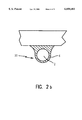
- FIG. 2b is a cross sectional view of an individual coated solder ball structure of an embodiment of the present invention.
- FIG. 3 is a cross sectional view of the contacting step of an alternative method of the current invention.
- FIG. 3a is a cross sectional view of a preferred embodiment of the contacting step of the method of the present invention.
- FIG. 4 is a cross sectional view of the a coated solder ball structure of an alternative embodiment of the present invention.
- FIG. 5 is a cross sectional view of an implementation of an alternative embodiment of the present invention; all in accordance with the present invention.
- the present invention can be used for connecting solder joints to any parts utilizing surface mount technology.
- electronic structures which require connection to other similar electronic structures or to other levels of package.
- New and creative connection protocols have necessitated the development of a new and different solder ball structures, including new collapsible solder ball structures.
- solder ball it is meant that a predetermined shape of a admixture of metals has been formed by any means known in the art and at least one reflow of the admixture has occurred.
- the admixture is typically of lead and tin.
- the shape of the admixture is left to the discretion of the user. It should be noted that according to the method and structure of the present invention a solder ball does not have to be spherical. For descriptive purposes only, the multitude of possible geometries will be referred to generally as solder balls.
- a high melting point, HMP, solder ball is encapsulated by a low melting point, LMP, solder.
- the terms low melting point, LMP, and high melting point, HMP, are not terms having specific temperatures associated with them.
- materials which are suitable include a eutectic solder of 37/63 weight percent Pb/Sn for the LMP material and a non-eutectic solder composition of 90/10 weight percent Pb/Sn for the HMP material.
- FIG. 1 a method of making the present invention is shown.
- the bottom of a solder ball, 2 is in contact with a BLM, 3, containing a LMP solder (LMP BLM).
- LMP BLM LMP solder
- BLM it is meant a ball limiting metallurgy structure.
- the BLM facilitates the electrical and physical connection of the admixture of solder with the first object.
- the BLM can be an integral part of the first object or formed on the first object.
- the BLM can be formed by any means known in the art as long as the necessary electrical and/or physical connection between the first object and the admixture of solder exists.
- the BLM, 3, may contain other components necessary to ensure proper electrical communication between the first object, 1, and the solder ball, 2.
- the BLM, 3, is in electrical communication with a first object, 1.
- the BLM can be formed and/or deposited by any means known in the art such that it can function with the first object.
- the first object, 1, is usually a substrate but the method and structure of the present invention are not limited by the composition of the first object, 1. For descriptive purposes only, the first object, 1, will hereafter be referred to as a substrate.
- the substrate, 1, containing the LMP BLM, 3, and HMP solder ball, 2 is brought into contact with a disjoint area of solder paste, 4, on a second object, 5.
- the shape of the disjoint area of LMP solder paste, 4, is determined by the user.
- a requirement of the subject invention is that the reflow of the LMP BLM and LMP solder paste occur without a significant portion of the HMP solder ball melting.
- a reflowing is accomplished while the solder ball 2 is in contact with the solder paste, 4.
- the reflowing can be accomplished by any means known in the art.
- the reflowing should occur at a temperature that is high enough to melt the LMP solder paste, 4, and the LMP solder BLM, 3, without melting a significant portion of the HMP solder ball, 2.
- a reflow will give the final form of the structure of one embodiment of the present invention (See FIG. 2b) where the HMP solder ball is essentially encapsulated in the LMP solder.
- the reflowing will take place at a temperature that will cause only the LMP solder in the BLM and the LMP solder paste to melt without a significant portion of the HMP solder ball melting.
- the solder ball diameter is 32 to 36.5 mils.
- the BLM and the solder paste would be a eutectic solder.
- the reflowed solder will be one homogeneous unit once it cools.
- the solder paste would be stencilled on the second object.
- the solder paste volume then would be measured.
- the volume of the solder paste would be at least about 8689 and at most about 11200 cubic mils and the solder paste volume would be measured using a laser tool.
- the height and diameter of the disjoint area of solder paste would also be controlled by the user.
- the diameter of the disjoint area of solder paste would be at least about 30 and at most about 34.5 mils.
- the height of the disjoint area of solder paste would be at least about 9 and at most about 16 mils.
- the solder paste volume would be about 11,000 cubic mils, the diameter would be about 34 mils and the height would be about 12 mils and the solder paste would be measured using a CybersentryTM laser tool.
- the second object, 5, would be a plate comprising high temperature glass or aluminum.
- the plate would be thin and flat.
- the plate, 5, would be coated with a non-wettable film, 7, that is heat resistant up to at least about 260° C.
- films, 7, include a polyimide tape like KaptonTM or a fluorocarbon copolymer like TeflonTM.
- the second object would be a thin, flat, high temperature resist, glass plate with a KaptonTM coating.
- the reflowing would be accomplished at a temperature of at least about 200° C. and at most about 205° C. Also in the preferred embodiment, the reflowing would be continued for at least about 20 seconds and at most about 30 seconds.
- FIG. 2b shows a final structure of the more preferred embodiment, 20, after the reflowing, where the BLM and the solder paste are both eutectic.
- the HMP solder ball, 2 is enclosed in the LMP solder ball coating, 6.
- the coating, 6, is formed from the reflowed BLM and solder paste.
- the coating, 6, is present over at least the portion of the solder ball surface not in contact with the corresponding BLM. In a preferred embodiment there would be no delineation between the portion of the coating, 6, that was contributed by the LMP solder paste, 4, and portion contributed by the LMP solder containing BLM, 3.
- the thickness of the coating is 2.5 mils.
- the HMP solder ball is comprised of 90% tin and 10% lead in admixture.
- FIG. 3 shows an embodiment of the present invention where a plurality of coated solder ball structures, 20 in FIG. 2b, would be formed at the same time.
- the individual HMP solder balls, 2, are similar in form to those shown in FIG. 1, where the BLM contains a LMP solder.
- the HMP solder balls, 2, contact the disjoint areas of LMP solder paste, 4.
- a reflow is then accomplished while the solder balls, 2, are in contact with the solder paste, 4.
- the after the reflow the structure as shown in FIG. 4 should exist where a LMP solder coating, 6, encapsulates each HMP solder ball, 2.
- the coating, 6, is present over at least the portion of the solder ball surface not in contact with the corresponding BLM.
- the distance between the top of the solder ball and the surface of the second object, A there is another factor that can be controlled.
- the shape of the final coated structure can be effected by the distance, A.
- the distance can be controlled by monitoring the distance, A, directly.
- An indirect measurement of A can also be achieved by monitoring the distance between the surface of the substrate, 1a, and the surface of the second object, 7a, if the distance between the substrate and the top of the solder ball is known or predictable.
- the substrate and the second object could be moved toward each other a predetermined distance such that the distance A is then maintained. In a most preferred embodiment the distance, A, is 7 mils.
- standoffs, 8, would be employed to ensure that the distance A was maintained as shown in FIG. 3a.
- the standoffs may be comprised of any material able to withstand temperatures of at least about 205° C.
- the standoffs would be located in an area where they would not interfere with the step of contacting the solder balls and the solder paste and could be attached to either the substrate or the second object prior to the contacting.
- the standoffs could be attached to neither the substrate nor the second object and could be inserted between the substrate and the second object by the same action that brings the substrate and the second object into contact with each other.
- the standoffs would be attached to the second object.
- FIG. 4 An example of the final structure, 20, that is achieved by the alternative embodiment shown above is shown in FIG. 4.
- the composition parameters for the HMP solder ball coating, 6, and the HMP solder ball 2 are the same as those for the solder ball shown in FIG. 2b.
- the substrate would be a module.
- the module would be a ceramic ball grid array.
- the structure of the present invention can be used to attach an object having the solder ball structure to a second object.
- the connection should at least be electrical.
- the connection could also be physical or mechanical.
- a LMP coated HMP solder ball can be used for direct chip attach to a circuit cards.
- LMP coated micro HMP solder balls can, be used on a chip attached to another substrate such as circuitized ceramic, polyimide, TeflonTM or plastic.
- the structure of the present invention can also be used in situations where coplanarity of the two objects being connected is a concern. Where one of the two objects to be connected can potentially be warped by more than 2 mils, the connection can be more effective if the solder balls are collapsible, as in the present embodiment.
- a circuit card may have more than a 2 mil warpage, for any number of reasons.
- the warpage may occur during manufacturing or it may be the result of heat fluctuations during a repair process.
- An embodiment of the structure of the present invention may be used when there is warpage greater than about 2 mils. in the second object.
- the thickness of the coating on the solder ball can be adjusted depending on the actual or predicted warpage of the second object.
- FIG. 5 shows an implementation of the structure of FIG. 4.
- a substrate, 1, with a plurality of distinct coated solder balls, 20, thereon is brought into contact with a second object, 10.
- the structure of the current invention is still operable if none of the coated solder balls are in contact with the circuit card, as long as they are proximally situated.
- proximally situated it is meant that the substrate and the circuit card are no more than a maximum distance from each other.
- the maximum distance is a function of ball size, pitch between the balls and the coating thickness.
- the present invention is operable when the maximum distance between the top of any individual coated solder ball and its corresponding pad is at most about 3.5 mils.
- the second object is a circuit card.
- the circuit card, 10, has a plurality of solder ball attachment points, 9. There is one attachment point, 9, for each solder ball structure, 20, connection desired.
- the attachment point, 9, is a copper pad which connects to the circuit card circuitry. It can be seen that due to warpage of the circuit card, 10, at least one of the attachment points, 9, may not be in contact with the corresponding coated solder ball, 20. A reflow is then accomplished. In a preferred embodiment, the reflow is accomplished while at least one of the coated solder balls, 20, is in contact with the corresponding attachment point, 9. In a more preferred embodiment a majority of the coated solder balls, 20, are in contact with the corresponding attachment point.
- each attachment point, 9, is coated with a material to facilitate the reflow.
- each attachment point is coated with a water soluble or no-clean flux paste.
- the reflow temperature is at least about 200° C. and at most about 220° C., the coating is 2.5 mils thick and the solder ball has a 35 mil diameter and a majority of the coated solder balls are in contact with the corresponding water soluble flux coated attachment points.
Abstract
Description
Claims (22)
Priority Applications (1)
| Application Number | Priority Date | Filing Date | Title |
|---|---|---|---|
| US08/882,459 US6050481A (en) | 1997-06-25 | 1997-06-25 | Method of making a high melting point solder ball coated with a low melting point solder |
Applications Claiming Priority (1)
| Application Number | Priority Date | Filing Date | Title |
|---|---|---|---|
| US08/882,459 US6050481A (en) | 1997-06-25 | 1997-06-25 | Method of making a high melting point solder ball coated with a low melting point solder |
Publications (1)
| Publication Number | Publication Date |
|---|---|
| US6050481A true US6050481A (en) | 2000-04-18 |
Family
ID=25380617
Family Applications (1)
| Application Number | Title | Priority Date | Filing Date |
|---|---|---|---|
| US08/882,459 Expired - Lifetime US6050481A (en) | 1997-06-25 | 1997-06-25 | Method of making a high melting point solder ball coated with a low melting point solder |
Country Status (1)
| Country | Link |
|---|---|
| US (1) | US6050481A (en) |
Cited By (20)
| Publication number | Priority date | Publication date | Assignee | Title |
|---|---|---|---|---|
| US6607613B2 (en) * | 1998-07-10 | 2003-08-19 | International Business Machines Corporation | Solder ball with chemically and mechanically enhanced surface properties |
| US20040108135A1 (en) * | 2002-10-11 | 2004-06-10 | Takeshi Ashida | Circuit board, mounting structure of ball grid array, electro-optic device and electronic device |
| US20070036670A1 (en) * | 2005-08-12 | 2007-02-15 | John Pereira | Solder composition |
| US20070037004A1 (en) * | 2005-08-12 | 2007-02-15 | Antaya Technologies Corporation | Multilayer solder article |
| US20070231594A1 (en) * | 2005-08-12 | 2007-10-04 | John Pereira | Multilayer solder article |
| US20070292708A1 (en) * | 2005-08-12 | 2007-12-20 | John Pereira | Solder composition |
| US20080175748A1 (en) * | 2005-08-12 | 2008-07-24 | John Pereira | Solder Composition |
| US20090166069A1 (en) * | 2005-07-28 | 2009-07-02 | Sharp Kabushiki Kaihsa | Solder Mounting Structure, Method for Manufacturing Such Solder Mounting Structure and Use of Such Solder Mounting Structure |
| US20090321949A1 (en) * | 2008-06-30 | 2009-12-31 | Huay Huay Sim | Backside mold process for ultra thin substrate and package on package assembly |
| US20100159645A1 (en) * | 1998-09-01 | 2010-06-24 | Sony Corporation | Semiconductor apparatus and process of production thereof |
| CN101132668B (en) * | 2006-08-23 | 2010-09-22 | 英业达股份有限公司 | Solder-paste coating method and instrument thereof |
| US20110139856A1 (en) * | 2009-12-11 | 2011-06-16 | Hitachi, Ltd. | Bonding structure and method for manufacturing same |
| US20120069528A1 (en) * | 2010-09-17 | 2012-03-22 | Irvine Sensors Corporation | Method for Control of Solder Collapse in Stacked Microelectronic Structure |
| US20140113446A1 (en) * | 2008-12-31 | 2014-04-24 | Stats Chippac, Ltd. | Semiconductor Device and Method of Confining Conductive Bump Material with Solder Mask Patch |
| CN104916579A (en) * | 2014-03-13 | 2015-09-16 | 台湾积体电路制造股份有限公司 | Semiconductor device structure and manufacturing method |
| US20150325507A1 (en) * | 2014-05-12 | 2015-11-12 | Invensas Corporation | Conductive connections, structures with such connections, and methods of manufacture |
| US20180020554A1 (en) * | 2012-03-20 | 2018-01-18 | Alpha Assembly Solutions Inc. | Solder Preforms and Solder Alloy Assembly Methods |
| US10049998B2 (en) | 2014-05-12 | 2018-08-14 | Invensas Corporation | Conductive connections, structures with such connections, and methods of manufacture |
| CN112378716A (en) * | 2020-09-30 | 2021-02-19 | 中国电子科技集团公司第十三研究所 | Sample preparation method for solderability test of CBGA device |
| US11830746B2 (en) * | 2021-01-05 | 2023-11-28 | Taiwan Semiconductor Manufacturing Co., Ltd. | Semiconductor device and method of manufacture |
Citations (13)
| Publication number | Priority date | Publication date | Assignee | Title |
|---|---|---|---|---|
| US4795554A (en) * | 1987-05-15 | 1989-01-03 | Carl Bernardi | PLCC co-planarity measurement method and apparatus |
| US5118027A (en) * | 1991-04-24 | 1992-06-02 | International Business Machines Corporation | Method of aligning and mounting solder balls to a substrate |
| US5147084A (en) * | 1990-07-18 | 1992-09-15 | International Business Machines Corporation | Interconnection structure and test method |
| US5154341A (en) * | 1990-12-06 | 1992-10-13 | Motorola Inc. | Noncollapsing multisolder interconnection |
| US5282565A (en) * | 1992-12-29 | 1994-02-01 | Motorola, Inc. | Solder bump interconnection formed using spaced solder deposit and consumable path |
| US5409157A (en) * | 1993-02-26 | 1995-04-25 | Nagesh; Voddarahalli K. | Composite transversely plastic interconnect for microchip carrier |
| US5480835A (en) * | 1993-05-06 | 1996-01-02 | Motorola, Inc. | Electrical interconnect and method for forming the same |
| US5529957A (en) * | 1995-04-06 | 1996-06-25 | Vlsi Technology, Inc. | Method for blocking contamination and stabilizing chip capacitor during attachment using a tape strip |
| US5542174A (en) * | 1994-09-15 | 1996-08-06 | Intel Corporation | Method and apparatus for forming solder balls and solder columns |
| US5586715A (en) * | 1994-08-08 | 1996-12-24 | Hewlett-Packard Company | Method of making solder balls by contained paste deposition |
| US5634268A (en) * | 1995-06-07 | 1997-06-03 | International Business Machines Corporation | Method for making direct chip attach circuit card |
| US5718361A (en) * | 1995-11-21 | 1998-02-17 | International Business Machines Corporation | Apparatus and method for forming mold for metallic material |
| US5729896A (en) * | 1996-10-31 | 1998-03-24 | International Business Machines Corporation | Method for attaching a flip chip on flexible circuit carrier using chip with metallic cap on solder |
-
1997
- 1997-06-25 US US08/882,459 patent/US6050481A/en not_active Expired - Lifetime
Patent Citations (13)
| Publication number | Priority date | Publication date | Assignee | Title |
|---|---|---|---|---|
| US4795554A (en) * | 1987-05-15 | 1989-01-03 | Carl Bernardi | PLCC co-planarity measurement method and apparatus |
| US5147084A (en) * | 1990-07-18 | 1992-09-15 | International Business Machines Corporation | Interconnection structure and test method |
| US5154341A (en) * | 1990-12-06 | 1992-10-13 | Motorola Inc. | Noncollapsing multisolder interconnection |
| US5118027A (en) * | 1991-04-24 | 1992-06-02 | International Business Machines Corporation | Method of aligning and mounting solder balls to a substrate |
| US5282565A (en) * | 1992-12-29 | 1994-02-01 | Motorola, Inc. | Solder bump interconnection formed using spaced solder deposit and consumable path |
| US5409157A (en) * | 1993-02-26 | 1995-04-25 | Nagesh; Voddarahalli K. | Composite transversely plastic interconnect for microchip carrier |
| US5480835A (en) * | 1993-05-06 | 1996-01-02 | Motorola, Inc. | Electrical interconnect and method for forming the same |
| US5586715A (en) * | 1994-08-08 | 1996-12-24 | Hewlett-Packard Company | Method of making solder balls by contained paste deposition |
| US5542174A (en) * | 1994-09-15 | 1996-08-06 | Intel Corporation | Method and apparatus for forming solder balls and solder columns |
| US5529957A (en) * | 1995-04-06 | 1996-06-25 | Vlsi Technology, Inc. | Method for blocking contamination and stabilizing chip capacitor during attachment using a tape strip |
| US5634268A (en) * | 1995-06-07 | 1997-06-03 | International Business Machines Corporation | Method for making direct chip attach circuit card |
| US5718361A (en) * | 1995-11-21 | 1998-02-17 | International Business Machines Corporation | Apparatus and method for forming mold for metallic material |
| US5729896A (en) * | 1996-10-31 | 1998-03-24 | International Business Machines Corporation | Method for attaching a flip chip on flexible circuit carrier using chip with metallic cap on solder |
Cited By (31)
| Publication number | Priority date | Publication date | Assignee | Title |
|---|---|---|---|---|
| US6607613B2 (en) * | 1998-07-10 | 2003-08-19 | International Business Machines Corporation | Solder ball with chemically and mechanically enhanced surface properties |
| US20100159645A1 (en) * | 1998-09-01 | 2010-06-24 | Sony Corporation | Semiconductor apparatus and process of production thereof |
| US20040108135A1 (en) * | 2002-10-11 | 2004-06-10 | Takeshi Ashida | Circuit board, mounting structure of ball grid array, electro-optic device and electronic device |
| US7268303B2 (en) * | 2002-10-11 | 2007-09-11 | Seiko Epson Corporation | Circuit board, mounting structure of ball grid array, electro-optic device and electronic device |
| US20090166069A1 (en) * | 2005-07-28 | 2009-07-02 | Sharp Kabushiki Kaihsa | Solder Mounting Structure, Method for Manufacturing Such Solder Mounting Structure and Use of Such Solder Mounting Structure |
| US20070292708A1 (en) * | 2005-08-12 | 2007-12-20 | John Pereira | Solder composition |
| US20080175748A1 (en) * | 2005-08-12 | 2008-07-24 | John Pereira | Solder Composition |
| US20070231594A1 (en) * | 2005-08-12 | 2007-10-04 | John Pereira | Multilayer solder article |
| US20070037004A1 (en) * | 2005-08-12 | 2007-02-15 | Antaya Technologies Corporation | Multilayer solder article |
| US20070036670A1 (en) * | 2005-08-12 | 2007-02-15 | John Pereira | Solder composition |
| CN101132668B (en) * | 2006-08-23 | 2010-09-22 | 英业达股份有限公司 | Solder-paste coating method and instrument thereof |
| US8384223B2 (en) * | 2008-06-30 | 2013-02-26 | Intel Corporation | Backside mold process for ultra thin substrate and package on package assembly |
| US20090321949A1 (en) * | 2008-06-30 | 2009-12-31 | Huay Huay Sim | Backside mold process for ultra thin substrate and package on package assembly |
| US8835220B2 (en) | 2008-06-30 | 2014-09-16 | Intel Corporation | Backside mold process for ultra thin substrate and package on package assembly |
| US9679811B2 (en) * | 2008-12-31 | 2017-06-13 | STATS ChipPAC Pte. Ltd. | Semiconductor device and method of confining conductive bump material with solder mask patch |
| US20140113446A1 (en) * | 2008-12-31 | 2014-04-24 | Stats Chippac, Ltd. | Semiconductor Device and Method of Confining Conductive Bump Material with Solder Mask Patch |
| US20110139856A1 (en) * | 2009-12-11 | 2011-06-16 | Hitachi, Ltd. | Bonding structure and method for manufacturing same |
| US8258637B2 (en) * | 2009-12-11 | 2012-09-04 | Hitachi, Ltd. | Bonding structure and method for manufacturing same |
| US20120069528A1 (en) * | 2010-09-17 | 2012-03-22 | Irvine Sensors Corporation | Method for Control of Solder Collapse in Stacked Microelectronic Structure |
| US20180020554A1 (en) * | 2012-03-20 | 2018-01-18 | Alpha Assembly Solutions Inc. | Solder Preforms and Solder Alloy Assembly Methods |
| CN104916579A (en) * | 2014-03-13 | 2015-09-16 | 台湾积体电路制造股份有限公司 | Semiconductor device structure and manufacturing method |
| US20150262953A1 (en) * | 2014-03-13 | 2015-09-17 | Taiwan Semiconductor Manufacturing Co., Ltd | Semiconductor device structure and manufacturing method |
| CN104916579B (en) * | 2014-03-13 | 2018-04-20 | 台湾积体电路制造股份有限公司 | Semiconductor device structure and manufacture method |
| US9735123B2 (en) * | 2014-03-13 | 2017-08-15 | Taiwan Semiconductor Manufacturing Company, Ltd. | Semiconductor device structure and manufacturing method |
| US9793198B2 (en) * | 2014-05-12 | 2017-10-17 | Invensas Corporation | Conductive connections, structures with such connections, and methods of manufacture |
| US20180019191A1 (en) * | 2014-05-12 | 2018-01-18 | Invensas Corporation | Conductive connections, structures with such connections, and methods of manufacture |
| US20150325507A1 (en) * | 2014-05-12 | 2015-11-12 | Invensas Corporation | Conductive connections, structures with such connections, and methods of manufacture |
| US10049998B2 (en) | 2014-05-12 | 2018-08-14 | Invensas Corporation | Conductive connections, structures with such connections, and methods of manufacture |
| US10090231B2 (en) * | 2014-05-12 | 2018-10-02 | Invensas Corporation | Conductive connections, structures with such connections, and methods of manufacture |
| CN112378716A (en) * | 2020-09-30 | 2021-02-19 | 中国电子科技集团公司第十三研究所 | Sample preparation method for solderability test of CBGA device |
| US11830746B2 (en) * | 2021-01-05 | 2023-11-28 | Taiwan Semiconductor Manufacturing Co., Ltd. | Semiconductor device and method of manufacture |
Similar Documents
| Publication | Publication Date | Title |
|---|---|---|
| US5872400A (en) | High melting point solder ball coated with a low melting point solder | |
| US6050481A (en) | Method of making a high melting point solder ball coated with a low melting point solder | |
| US6084781A (en) | Assembly aid for mounting packaged integrated circuit devices to printed circuit boards | |
| US6281581B1 (en) | Substrate structure for improving attachment reliability of semiconductor chips and modules | |
| US5435732A (en) | Flexible circuit member | |
| US6165885A (en) | Method of making components with solder balls | |
| US5060844A (en) | Interconnection structure and test method | |
| US7145236B2 (en) | Semiconductor device having solder bumps reliably reflow solderable | |
| US5658827A (en) | Method for forming solder balls on a substrate | |
| US6307160B1 (en) | High-strength solder interconnect for copper/electroless nickel/immersion gold metallization solder pad and method | |
| US5477419A (en) | Method and apparatus for electrically connecting an electronic part to a circuit board | |
| US5133495A (en) | Method of bonding flexible circuit to circuitized substrate to provide electrical connection therebetween | |
| US5147084A (en) | Interconnection structure and test method | |
| US5203075A (en) | Method of bonding flexible circuit to cicuitized substrate to provide electrical connection therebetween using different solders | |
| US6059172A (en) | Method for establishing electrical communication between a first object having a solder ball and a second object | |
| US5172852A (en) | Soldering method | |
| US5736790A (en) | Semiconductor chip, package and semiconductor device | |
| US5936309A (en) | Mounted structure of printed circuit board in semiconductor package | |
| US6870267B2 (en) | Off-center solder ball attach assembly | |
| US6727718B2 (en) | Electronic component package, printed circuit board, and method of inspecting the printed circuit board | |
| US5868304A (en) | Socketable bump grid array shaped-solder on copper spheres | |
| Ghosal et al. | Ceramic and Plastic Pin Grid Array Technology | |
| JP3180041B2 (en) | Connection terminal and method of forming the same | |
| US6070782A (en) | Socketable bump grid array shaped-solder on copper spheres | |
| JP2000151086A (en) | Printed circuit unit and its manufacture |
Legal Events
| Date | Code | Title | Description |
|---|---|---|---|
| AS | Assignment |
Owner name: INTERNATIONAL BUSINESS MACHINES CORPORATION, NEW Y Free format text: ASSIGNMENT OF ASSIGNORS INTEREST;ASSIGNORS:CHAPMAN, BRIAN D.;MA, WAI MON;PETRONE, JAMES J.;REEL/FRAME:008664/0849 Effective date: 19970624 |
|
| STCF | Information on status: patent grant |
Free format text: PATENTED CASE |
|
| FEPP | Fee payment procedure |
Free format text: PAYOR NUMBER ASSIGNED (ORIGINAL EVENT CODE: ASPN); ENTITY STATUS OF PATENT OWNER: LARGE ENTITY |
|
| FPAY | Fee payment |
Year of fee payment: 4 |
|
| REMI | Maintenance fee reminder mailed | ||
| FPAY | Fee payment |
Year of fee payment: 8 |
|
| SULP | Surcharge for late payment |
Year of fee payment: 7 |
|
| FPAY | Fee payment |
Year of fee payment: 12 |
|
| AS | Assignment |
Owner name: ULTRATECH, INC., CALIFORNIA Free format text: ASSIGNMENT OF ASSIGNORS INTEREST;ASSIGNOR:INTERNATIONAL BUSINESS MACHINES CORPORATION;REEL/FRAME:028964/0014 Effective date: 20120718 |