US6049101A - Processing methods of forming a capacitor, and capacitor construction - Google Patents
Processing methods of forming a capacitor, and capacitor construction Download PDFInfo
- Publication number
- US6049101A US6049101A US09/036,702 US3670298A US6049101A US 6049101 A US6049101 A US 6049101A US 3670298 A US3670298 A US 3670298A US 6049101 A US6049101 A US 6049101A
- Authority
- US
- United States
- Prior art keywords
- capacitor
- conductive material
- opening
- protuberant
- node location
- Prior art date
- Legal status (The legal status is an assumption and is not a legal conclusion. Google has not performed a legal analysis and makes no representation as to the accuracy of the status listed.)
- Expired - Lifetime
Links
Images


Classifications
-
- H—ELECTRICITY
- H01—ELECTRIC ELEMENTS
- H01L—SEMICONDUCTOR DEVICES NOT COVERED BY CLASS H10
- H01L28/00—Passive two-terminal components without a potential-jump or surface barrier for integrated circuits; Details thereof; Multistep manufacturing processes therefor
- H01L28/40—Capacitors
- H01L28/60—Electrodes
- H01L28/82—Electrodes with an enlarged surface, e.g. formed by texturisation
- H01L28/90—Electrodes with an enlarged surface, e.g. formed by texturisation having vertical extensions
- H01L28/91—Electrodes with an enlarged surface, e.g. formed by texturisation having vertical extensions made by depositing layers, e.g. by depositing alternating conductive and insulating layers
-
- H—ELECTRICITY
- H01—ELECTRIC ELEMENTS
- H01L—SEMICONDUCTOR DEVICES NOT COVERED BY CLASS H10
- H01L28/00—Passive two-terminal components without a potential-jump or surface barrier for integrated circuits; Details thereof; Multistep manufacturing processes therefor
- H01L28/40—Capacitors
- H01L28/60—Electrodes
- H01L28/82—Electrodes with an enlarged surface, e.g. formed by texturisation
- H01L28/84—Electrodes with an enlarged surface, e.g. formed by texturisation being a rough surface, e.g. using hemispherical grains
-
- H—ELECTRICITY
- H10—SEMICONDUCTOR DEVICES; ELECTRIC SOLID-STATE DEVICES NOT OTHERWISE PROVIDED FOR
- H10B—ELECTRONIC MEMORY DEVICES
- H10B12/00—Dynamic random access memory [DRAM] devices
- H10B12/01—Manufacture or treatment
- H10B12/02—Manufacture or treatment for one transistor one-capacitor [1T-1C] memory cells
- H10B12/03—Making the capacitor or connections thereto
- H10B12/033—Making the capacitor or connections thereto the capacitor extending over the transistor
-
- H—ELECTRICITY
- H10—SEMICONDUCTOR DEVICES; ELECTRIC SOLID-STATE DEVICES NOT OTHERWISE PROVIDED FOR
- H10B—ELECTRONIC MEMORY DEVICES
- H10B12/00—Dynamic random access memory [DRAM] devices
- H10B12/30—DRAM devices comprising one-transistor - one-capacitor [1T-1C] memory cells
- H10B12/31—DRAM devices comprising one-transistor - one-capacitor [1T-1C] memory cells having a storage electrode stacked over the transistor
- H10B12/318—DRAM devices comprising one-transistor - one-capacitor [1T-1C] memory cells having a storage electrode stacked over the transistor the storage electrode having multiple segments
Definitions
- This invention relates generally to capacitors and to capacitor formation in semiconductor wafer processing.
- cell structure techniques include three-dimensional cell capacitors, such as trenched or stacked capacitors.
- This invention concerns three-dimensional cell capacitor constructions and methods of forming the same.
- a capacitor opening is formed over a substrate node location. Electrically conductive material is subsequently formed within the capacitor opening and makes an electrical connection with the node location.
- a protuberant insulative structure is formed within the capacitor opening and includes a lateral outer surface at least a portion of which is supported by and extends elevationally below adjacent conductive material.
- the conductive material is formed to occupy less than all of the capacitor opening and to leave a void therewithin, with the protuberant structure substantially, if not completely filling in the void.
- the conductive material is formed to occupy less than all of the capacitor opening and to leave a void therewithin, with the protuberant structure only partially filling in the void to provide a tubular structure.
- First and second capacitor plates and a dielectric layer therebetween are formed within the capacitor opening and supported by the protuberant structure.
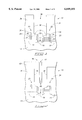
- FIG. 1 is a diagrammatic sectional view of a semiconductor wafer fragment at one processing step in accordance with one implementation of the invention.
- FIG. 2 is a view of the FIG. 1 wafer fragment at a processing step subsequent to that shown by FIG. 1.
- FIG. 3 is a view of the FIG. 1 wafer fragment at a processing step subsequent to that shown by FIG. 2.
- FIG. 4 is a view of the FIG. 1 wafer fragment at a processing step subsequent to that shown by FIG. 3.
- FIG. 5 is a view of the FIG. 1 wafer fragment at a processing step subsequent to that shown by FIG. 4.
- FIG. 6 is a view of the FIG. 1 wafer fragment at a processing step subsequent to that shown by FIG. 5.
- FIG. 7 is a view of the FIG. 1 wafer fragment at a processing step subsequent to that shown by FIG. 6.
- FIG. 8 is a diagrammatic sectional view of a semiconductor wafer fragment at one processing step in accordance with another implementation of the invention.
- FIG. 9 is a view of the FIG. 8 wafer fragment at a processing step subsequent to that shown by FIG. 8.
- FIG. 10 is a view of the FIG. 8 wafer fragment at a processing step subsequent to that shown by FIG. 9.
- FIG. 11 is a view taken along line 11--11 in FIG. 10.
- FIG. 12 is a view of the FIG. 8 wafer fragment at a processing step subsequent to that shown by FIG. 10.
- FIG. 13 is a diagrammatic sectional view of a semiconductor wafer fragment at one processing step in accordance with another implementation of the invention.
- FIG. 14 is a view of the FIG. 13 wafer fragment at a processing step subsequent to that shown by FIG. 13.
- FIG. 15 is a view of the FIG. 13 wafer fragment at a processing step subsequent to that shown by FIG. 14.
- FIG. 16 is a view of the FIG. 13 wafer fragment at a processing step subsequent to that shown by FIG. 15.
- a semiconductor wafer fragment in process is indicated generally with reference numeral 10 and comprises a semiconductive substrate 12.
- semiconductive substrate is defined to mean any construction comprising semiconductive material, including, but not limited to, bulk semiconductive materials such as a semiconductive wafer (either alone or in assemblies comprising other materials thereon), and semiconductive material layers (either alone or in assemblies comprising other material).
- substrate refers to any supporting structure, including, but not limited to, the semiconductive substrates described above.
- the illustrated substrate includes an isolation region defined by isolation oxide 14 which is formed adjacent a substrate active area which includes diffusion regions 16, 18 received therein.
- Conductive lines 20, 22 are formed over substrate 12 and constitute part of the preferred DRAM circuitry.
- Conductive lines 20, 22 are of standard construction and include an oxide layer 24, a polysilicon layer 26, and a silicide layer 28.
- Conductive lines 20, 22 also include respective sidewall spacers 30 and respective protective caps 32.
- An electrically insulative layer 34 is formed over substrate 12 and conductive lines 20, 22.
- Layer 34 preferably comprises an oxide material, such as borophosphosilicate glass (BPSG).
- An initial capacitor contact opening 36 is etched or otherwise formed through layer 34 to the outer surface of diffusion region 16, which for the purposes of the continuing discussion comprises an example node location 17.
- Capacitor contact opening 36 constitutes a container relative to which a storage capacitor will be formed. Such container can be formed by a self-aligned contact etch which contacts the active area region as shown. Alternately, the container can make an electrical connection with a previously formed plug of conductive material such as polysilicon, which in turn, forms a connection with the active area region of the substrate.
- capacitor contact opening 36 has an inner sidewall surface area 38 defined by insulative layer 34 and spaced from node location 17. Accordingly, such defines a capacitor opening which is disposed elevationally over node location 17.
- a layer of electrically conductive material 40 is formed over substrate 12 and within capacitor opening 36 and makes electrical connection with node location 17.
- a preferred conductive material is in situ doped polysilicon.
- Conductive material 40 is formed over inner sidewall surface area 38 and preferably occupies less than all of capacitor opening 36 as shown. Accordingly, such leaves a void 42 outwardly of node location 17 which is defined, at least in part, by a conductive material sidewall 44.
- void 42 and sidewall 44 define a conductive female receptacle or pocket of female conductive material which is formed within capacitor opening 36. In the illustrated example, at least some portion of the conductive receptacle or pocket material makes an electrical connection with node location 17.
- Conductive material 40 can be, and preferably is deposited to a thickness which both achieves an adequate electrical connection between a to-be-formed capacitor and node location 17, and enables selected conductive material to be used as a sacrificial spacer layer as will become apparent below.
- a layer of insulative material 46 is deposited or formed over the substrate and within at least a portion, and preferably the entirety of void or pocket 42.
- portions of insulative material 46 are formed adjacent and in contact with conductive material 40.
- insulative material is formed over conductive material sidewall 44 and completely fills void 42.
- Suitable materials for insulative material 46 include oxides of silicon, i.e. SiO 2 , and nitrides of silicon, i.e. Si 3 N 4 , with the latter being preferred for achieving desirable step coverage. Of course, other suitable insulative materials can be used.
- portions of insulative material 46 and conductive material 40 are preferably removed to a degree sufficient to leave behind only material which was deposited or formed within capacitor contact opening 36. Accordingly, only insulative material which was formed or deposited within that portion of void or pocket 42 disposed within contact opening 36 remains.
- the removal of such material can be effectuated by conventional techniques such as abrasion of the substrate by chemical mechanical polishing or through a dry etch back process. Other techniques can, of course, be used.
- an amount of conductive material 40 laterally adjacent inner sidewall surface area 38 is removed to define a conductive upper surface 41 and to expose a protuberant insulative support structure or male projection 48 which is formed within capacitor opening 36.
- Upper surface 41 is elevationally spaced from node location 17 by virtue of remaining conductive material 40 therebetween.
- upper surface 41 is generally planar.
- Structure or projection 48 defines a column of insulative material which is spaced from inner sidewall surface area 38 as shown, and which includes a lateral outer surface 50 at least a portion of which is supported by and extends elevationally below adjacent electrically conductive material 40.
- structure or projection 48 includes an interior region laterally adjacent outer surface 50 which is substantially, if not completely filled with insulative material.
- structure or projection 48 is formed from decomposition of tetraethyl orthosilicate (TEOS) with a resulting construction which has a key hole void at or adjacent the top of the structure. Accordingly, such structure or projection is not completely filled with insulative material.
- TEOS tetraethyl orthosilicate
- conductive material 40 (FIG. 4) is removed substantially selectively relative to insulative material 46 and to a degree which is sufficient to expose sidewall surface area 38 laterally adjacent lateral outer surface 50. Removal of conductive material 40 is effectuated through a wet or dry etch thereof (with a dry etch being preferred) relative to insulative material 46 and insulative material 34. Where insulative material 46 comprises an oxide of silicon, such etch would accordingly be selective relative to the oxide of silicon. Where insulative material 46 comprises a nitride of silicon, such etch would accordingly be selective relative to the nitride of silicon. Such etch is also preferably selective relative to insulative material 34. Exemplary etch chemistries include one or more of the following: TMAH/H 2 O mix, nitric/hydrofluoric mix, 15% aqueous KOH, or 5% aqueous choline.
- conductive material 40 comprises polysilicon and the removal thereof is desired to be selective to oxide
- the following etch chemistries are preferred: chlorine-based chemistries such as Cl 2 , BCl 3 , SiCl 4 , or HCl; bromine-based chemistries such as HBr; and/or combinations of the above, e.g. HBr+HCl.
- a wet etch thereof is more preferred.
- the etching of conductive material 40 is preferably a timed etch which is conducted to a degree sufficient to leave at least some conductive material laterally outward of and below structure or projection 48 to support the same. Accordingly, structure or projection 48 is supported interiorly of capacitor opening 36 with conductive material which forms an electrical connection or contact with substrate diffusion region 16.
- the portion of structure or projection 48 which extends a selected distance elevationally below conductive material upper surface 41 is defined by the duration of the timed etch mentioned above. Accordingly, the structure or projection is outwardly supported by that portion of conductive material 40 which is not removed, and hence extends elevationally outwardly or above and below surface 41.
- structure 48 defines an upright insulative structure which includes lateral outer sidewall surface 50 which is disposed elevationally outwardly of an insulative structure bottom portion or base 52. Bottom portion 52 and at least a portion of the lateral outer sidewall surface are supported with conductive material 40 which forms an electrical connection with node location 17.
- Lateral outer surface 50 constitutes an insulative surface which is disposed laterally adjacent insulative sidewall 38. Insulative surface 50 includes an area, at least a portion of which is supported with conductive material 40. In the illustrated example, the conductive material which supports such insulative surface area extends laterally between insulative surface 50 and insulative sidewall 38.
- structure, projection, or column 48 is formed to define an elongate column. Column 48 can have circular and non-circular transverse cross sections.
- first capacitor plate structure 56 is formed within capacitor opening 36 at least a portion of which is supported by structure 48. Accordingly, at least some of plate structure 56 is formed over capacitor opening sidewall surface 38 and protuberant structure lateral outer surface 50.
- First capacitor plate structure 56 can comprise any suitable material. Exemplary and preferred materials include polysilicon, polysilicon in combination with a hemispherical grain (HSG) polysilicon, or in situ doped HSG. The selected material is preferably formed over the substrate and deposited within contact opening 36 to a thickness from between about 300 to 600 Angstroms. Subsequently, such material is planarized as by suitable mechanical abrasion of the substrate to remove such material from outwardly of contact opening 36.
- HSG hemispherical grain
- capacitor contact opening 36 is filled with photoresist to prevent removed particles from falling into the opening during planarization or to prevent etching of the material inside opening 36 during the dry etch back process.
- the photoresist is subsequently removed.
- cell nitride is deposited over first capacitor plate structure 56 followed by an oxidation step to form the illustrated ONO dielectric layer 58.
- a second capacitor plate structure 60 is provided or formed operatively adjacent the first capacitor plate structure 56 to provide a storage cell which, in the illustrated and preferred embodiment, constitutes a portion of DRAM circuitry.
- such second capacitor plate structure comprises polysilicon.
- Subsequent processing to form bit line contact plugs and bit lines can take place in a manner which will be understood by one of skill in the art.
- a layer of conductive material 40a is formed within capacitor opening 36 to occupy less than all of the capacitor opening and to leave a void or female receptacle 42a outwardly of node location 17.
- An insulative material layer 46a preferably comprising a nitride material or conformal oxide, is formed over substrate 12 and preferably within capacitor opening 36. Portions of the insulative material are subsequently removed to leave remnant insulative material 47 in the form of a spacer (preferably a hollowed annular column or tube) over conductive material sidewall 44a.
- insulative material 46a is anisotropically etched adjacent conductive material 40a to leave the spacer thereover. Accordingly, such etching forms a tubular column of insulative material within capacitor opening 36. Subsequently, a photoresist material 43 can be provided within void or receptacle 42a and over conductive material 40a.
- portions of conductive material 40a and insulative material 46a can be removed as by suitable resist etch back techniques or abrasion of substrate 12. Such constitutes planarizing or etching back conductive material 40a and insulative material 46a relative to the upper surface of insulative material 34.
- the above-mentioned photoresist 43 which is provided into receptacle 42a prevents debris from falling into receptacle 42a during the planarization or etch back.
- material 40a is etched selectively relative to the material from which spacer 47 was formed and insulative material 34.
- the photoresist can then be stripped through conventional means to give the FIG. 10 construction. Accordingly, such defines a protuberant structure, projection or support column 48a of insulative material.
- conductive material 40a exposes a column surface 50a laterally adjacent capacitor opening inner sidewall surface area 38.
- column 48a at least a portion of column 48a and preferably all of such column is tubular and includes an exposed inside or inner surface 51.
- Structure or column 48a constitutes insulative material which partially fills female receptacle 42a.
- conductive material 40a defies an upper surface 41a which includes a portion which is generally non-planar laterally inwardly of inner surface 51.
- a portion of upper surface 41a laterally outwardly of inner surface 51 is generally planar.
- One manner of effectuating the 41'a construction is through a suitable anisotropic etch of material 40a which is conducted substantially selective relative to insulative material 34 and spacer 47.
- etch can include an isotropic etch of material 40a to produce a somewhat outwardly rounded or bulbed construction indicated at 41"a.
- etch of material 40a can be entirely isotropic and conducted substantially selective relative to insulative material 34 and spacer 47.
- a first capacitor plate structure 56a is formed within the capacitor opening and preferably over and within tubular projection 48a.
- such plate structure is formed over outer surface 50a and inner or inside surface 51 as shown. Accordingly, such plate structure is formed over lateral outer sidewall surface 50a which is unsupported with any of the conductive material.
- a dielectric layer 58a and a second capacitor plate structure 60a are provided or formed operatively adjacent first capacitor plate structure 56a.
- FIG. 13 another alternate preferred embodiment is set forth generally at 10b. Like numbers from the embodiment of FIGS. 9-12 are utilized where appropriate, with differences being indicated with the suffix "b" or with different numerals. Processing in accordance with this aspect of the invention takes place in substantially the same manner up to and including the resultant FIG. 9 construction. Subsequently, a layer 62 comprising conductive material is deposited or otherwise formed over substrate 12. Preferably layer 62 material completely fills void or pocket 42a. Accordingly, such constitutes completely filling an area interiorly of remnant spacer material 47 with conductive material. An exemplary material for layer 62 comprises polysilicon.
- layer 62, layer 40a, and portions of remnant spacer material 47 are planarized as by suitable mechanical abrasion of substrate 12. Such leaves a core 64 of conductive material interiorly of remnant spacer material 47.
- An exemplary abrading process is chemical mechanical polishing.
- the conductive material comprising both layer 40a and core 64 is selectively removed relative to structure, projection, or column 48a to expose a column surface 50a laterally adjacent capacitor opening inner sidewall surface area 38.
- Such can be accomplished with either a wet or a dry etch.
- at least a portion of column 48a and preferably all of such column is tubular and includes an exposed inside or inner surface 51.
- Structure or column 48a constitutes insulative material which partially fills female receptacle 42a.
- conductive material 40a defines an upper surface 41b which is generally planar laterally proximate inner surface 51.
- upper surface 41b includes portions which are generally planar both laterally inwardly and laterally outwardly of inner surface 51.
- a first capacitor plate structure 56b is formed within the capacitor opening and preferably over and within tubular projection 48a.
- such plate structure is formed over outer surface 50a, inner or inside surface 51, and the remaining core material 64 as shown. Accordingly, such plate structure is formed over lateral outer sidewall surface 50a which is unsupported with any of the conductive material.
- a dielectric layer 58b and a second capacitor plate structure 60b are provided or formed operatively adjacent first capacitor plate structure 56b.
- the above described invention increases the surface area available for accommodating or supporting storage capacitors.
- the invention has particular applicability in DRAM circuitry.
Abstract
Description
Claims (10)
Priority Applications (2)
| Application Number | Priority Date | Filing Date | Title |
|---|---|---|---|
| US09/036,702 US6049101A (en) | 1997-06-23 | 1998-03-06 | Processing methods of forming a capacitor, and capacitor construction |
| US09/497,935 US6580114B1 (en) | 1997-06-23 | 2000-02-04 | Processing methods of forming a capacitor, and capacitor construction |
Applications Claiming Priority (2)
| Application Number | Priority Date | Filing Date | Title |
|---|---|---|---|
| US08/880,356 US6146961A (en) | 1997-06-23 | 1997-06-23 | Processing methods of forming a capacitor |
| US09/036,702 US6049101A (en) | 1997-06-23 | 1998-03-06 | Processing methods of forming a capacitor, and capacitor construction |
Related Parent Applications (1)
| Application Number | Title | Priority Date | Filing Date |
|---|---|---|---|
| US08/880,356 Division US6146961A (en) | 1997-06-23 | 1997-06-23 | Processing methods of forming a capacitor |
Related Child Applications (1)
| Application Number | Title | Priority Date | Filing Date |
|---|---|---|---|
| US09/497,935 Continuation US6580114B1 (en) | 1997-06-23 | 2000-02-04 | Processing methods of forming a capacitor, and capacitor construction |
Publications (1)
| Publication Number | Publication Date |
|---|---|
| US6049101A true US6049101A (en) | 2000-04-11 |
Family
ID=25376085
Family Applications (3)
| Application Number | Title | Priority Date | Filing Date |
|---|---|---|---|
| US08/880,356 Expired - Lifetime US6146961A (en) | 1997-06-23 | 1997-06-23 | Processing methods of forming a capacitor |
| US09/036,702 Expired - Lifetime US6049101A (en) | 1997-06-23 | 1998-03-06 | Processing methods of forming a capacitor, and capacitor construction |
| US09/497,935 Expired - Lifetime US6580114B1 (en) | 1997-06-23 | 2000-02-04 | Processing methods of forming a capacitor, and capacitor construction |
Family Applications Before (1)
| Application Number | Title | Priority Date | Filing Date |
|---|---|---|---|
| US08/880,356 Expired - Lifetime US6146961A (en) | 1997-06-23 | 1997-06-23 | Processing methods of forming a capacitor |
Family Applications After (1)
| Application Number | Title | Priority Date | Filing Date |
|---|---|---|---|
| US09/497,935 Expired - Lifetime US6580114B1 (en) | 1997-06-23 | 2000-02-04 | Processing methods of forming a capacitor, and capacitor construction |
Country Status (1)
| Country | Link |
|---|---|
| US (3) | US6146961A (en) |
Cited By (12)
| Publication number | Priority date | Publication date | Assignee | Title |
|---|---|---|---|---|
| US6297121B1 (en) * | 2000-08-16 | 2001-10-02 | Vanguard International Semiconductor Corporation | Fabrication method for capacitors in integrated circuits with a self-aligned contact structure |
| US20020024084A1 (en) * | 2000-08-25 | 2002-02-28 | Coursey Belford T. | Memory Circuity and Dynamic Random Access Memory Circuity Memory Circuity and Dynamic Random |
| US6396679B1 (en) | 2000-10-18 | 2002-05-28 | Trw Inc. | Single-layer dielectric structure with rounded corners, and circuits including such structures |
| US6429127B1 (en) | 2000-06-08 | 2002-08-06 | Micron Technology, Inc. | Methods for forming rough ruthenium-containing layers and structures/methods using same |
| US6482736B1 (en) | 2000-06-08 | 2002-11-19 | Micron Technology, Inc. | Methods for forming and integrated circuit structures containing enhanced-surface-area conductive layers |
| US20030003697A1 (en) * | 2000-06-08 | 2003-01-02 | Micron Techology, Inc. | Methods for forming and integrated circuit structures containing ruthenium and tungsten containing layers |
| US6784069B1 (en) | 2003-08-29 | 2004-08-31 | Micron Technology, Inc. | Permeable capacitor electrode |
| KR100450678B1 (en) * | 2002-07-10 | 2004-10-01 | 삼성전자주식회사 | Semiconductor memory device comprising two-story capacitor bottom electrode and method of manufacturing the same |
| US20040212445A1 (en) * | 2003-04-22 | 2004-10-28 | Haglan David E. | Filter method and apparatus for polar modulation |
| US20050032346A1 (en) * | 2003-08-05 | 2005-02-10 | Graettinger Thomas M. | Stud electrode and process for making same |
| US20060033140A1 (en) * | 2004-08-13 | 2006-02-16 | Graettinger Thomas M | Memory circuitry |
| US20230326957A1 (en) * | 2022-04-08 | 2023-10-12 | Nanya Technology Corporation | Semiconductor structure and method of forming the same |
Families Citing this family (6)
| Publication number | Priority date | Publication date | Assignee | Title |
|---|---|---|---|---|
| US6566236B1 (en) * | 2000-04-26 | 2003-05-20 | Integrated Device Technology, Inc. | Gate structures with increased etch margin for self-aligned contact and the method of forming the same |
| US6277688B1 (en) * | 2000-06-30 | 2001-08-21 | Vanguard International Semiconductor Corporation | Method of manufacturing a DRAM capacitor with increased electrode surface area |
| US6319771B1 (en) * | 2000-07-21 | 2001-11-20 | Vanguard International Semiconductor Corp. | Fabrication process for a lower electrode of a memory capacitor |
| KR100363702B1 (en) * | 2000-12-29 | 2002-12-05 | 주식회사 하이닉스반도체 | Storage node contact plug of semiconductor device and method for forming thereof |
| US6492245B1 (en) | 2001-10-16 | 2002-12-10 | Taiwan Semiconductor Manufacturing Company | Method of forming air gap isolation between a bit line contact structure and a capacitor under bit line structure |
| JP4569924B2 (en) * | 2005-04-08 | 2010-10-27 | エルピーダメモリ株式会社 | Manufacturing method of semiconductor device |
Citations (10)
| Publication number | Priority date | Publication date | Assignee | Title |
|---|---|---|---|---|
| JPH03257859A (en) * | 1990-03-07 | 1991-11-18 | Mitsubishi Electric Corp | Semiconductor device and manufacture thereof |
| US5126916A (en) * | 1991-12-20 | 1992-06-30 | Industrial Technology Research Institute | Stacked capacitor dram cell and method of fabricating |
| US5126280A (en) * | 1991-02-08 | 1992-06-30 | Micron Technology, Inc. | Stacked multi-poly spacers with double cell plate capacitor |
| US5150276A (en) * | 1992-01-24 | 1992-09-22 | Micron Technology, Inc. | Method of fabricating a vertical parallel cell capacitor having a storage node capacitor plate comprising a center fin effecting electrical communication between itself and parallel annular rings |
| US5364809A (en) * | 1991-05-23 | 1994-11-15 | Samsung Electronics Co., Ltd. | Method of fabricating a capacitor for a dynamic random access memory cell |
| US5438011A (en) * | 1995-03-03 | 1995-08-01 | Micron Technology, Inc. | Method of forming a capacitor using a photoresist contact sidewall having standing wave ripples |
| US5661320A (en) * | 1993-08-09 | 1997-08-26 | Sony Corporation | Semiconductor device and method of manufacturing the same |
| US5723889A (en) * | 1994-11-21 | 1998-03-03 | Lg Semicon Co., Ltd. | Semiconductor memory device and method for fabricating the same |
| US5821139A (en) * | 1996-10-07 | 1998-10-13 | Vanguard International Semiconductor Corporation | Method for manufacturing a DRAM with increased electrode surface area |
| US5837577A (en) * | 1998-04-24 | 1998-11-17 | Vanguard International Semiconductor Corporation | Method for making self-aligned node contacts to bit lines for capacitor-over-bit-line structures on dynamic random access memory (DRAM) devices |
Family Cites Families (4)
| Publication number | Priority date | Publication date | Assignee | Title |
|---|---|---|---|---|
| JP3257859B2 (en) | 1993-05-14 | 2002-02-18 | 積水化学工業株式会社 | Parapet connection structure |
| KR0132831B1 (en) * | 1994-07-08 | 1998-04-16 | 김광호 | Manufacturing method of semiconductor device cell with buried bit line and pin structured capacitor |
| US5605864A (en) * | 1994-08-02 | 1997-02-25 | Micron Technology, Inc. | Method for forming a semiconductor buried contact with a removable spacer |
| US5700706A (en) * | 1995-12-15 | 1997-12-23 | Micron Technology, Inc. | Self-aligned isolated polysilicon plugged contacts |
-
1997
- 1997-06-23 US US08/880,356 patent/US6146961A/en not_active Expired - Lifetime
-
1998
- 1998-03-06 US US09/036,702 patent/US6049101A/en not_active Expired - Lifetime
-
2000
- 2000-02-04 US US09/497,935 patent/US6580114B1/en not_active Expired - Lifetime
Patent Citations (10)
| Publication number | Priority date | Publication date | Assignee | Title |
|---|---|---|---|---|
| JPH03257859A (en) * | 1990-03-07 | 1991-11-18 | Mitsubishi Electric Corp | Semiconductor device and manufacture thereof |
| US5126280A (en) * | 1991-02-08 | 1992-06-30 | Micron Technology, Inc. | Stacked multi-poly spacers with double cell plate capacitor |
| US5364809A (en) * | 1991-05-23 | 1994-11-15 | Samsung Electronics Co., Ltd. | Method of fabricating a capacitor for a dynamic random access memory cell |
| US5126916A (en) * | 1991-12-20 | 1992-06-30 | Industrial Technology Research Institute | Stacked capacitor dram cell and method of fabricating |
| US5150276A (en) * | 1992-01-24 | 1992-09-22 | Micron Technology, Inc. | Method of fabricating a vertical parallel cell capacitor having a storage node capacitor plate comprising a center fin effecting electrical communication between itself and parallel annular rings |
| US5661320A (en) * | 1993-08-09 | 1997-08-26 | Sony Corporation | Semiconductor device and method of manufacturing the same |
| US5723889A (en) * | 1994-11-21 | 1998-03-03 | Lg Semicon Co., Ltd. | Semiconductor memory device and method for fabricating the same |
| US5438011A (en) * | 1995-03-03 | 1995-08-01 | Micron Technology, Inc. | Method of forming a capacitor using a photoresist contact sidewall having standing wave ripples |
| US5821139A (en) * | 1996-10-07 | 1998-10-13 | Vanguard International Semiconductor Corporation | Method for manufacturing a DRAM with increased electrode surface area |
| US5837577A (en) * | 1998-04-24 | 1998-11-17 | Vanguard International Semiconductor Corporation | Method for making self-aligned node contacts to bit lines for capacitor-over-bit-line structures on dynamic random access memory (DRAM) devices |
Cited By (40)
| Publication number | Priority date | Publication date | Assignee | Title |
|---|---|---|---|---|
| US6764943B2 (en) | 2000-06-08 | 2004-07-20 | Micron Technology, Inc. | Methods for forming and integrated circuit structures containing enhanced-surface-area conductive layers |
| US6596583B2 (en) | 2000-06-08 | 2003-07-22 | Micron Technology, Inc. | Methods for forming and integrated circuit structures containing ruthenium and tungsten containing layers |
| US20060076597A1 (en) * | 2000-06-08 | 2006-04-13 | Micron Technology, Inc. | Methods for forming and integrated circuit structures containing ruthenium and tungsten containing layers |
| US6429127B1 (en) | 2000-06-08 | 2002-08-06 | Micron Technology, Inc. | Methods for forming rough ruthenium-containing layers and structures/methods using same |
| US7253102B2 (en) | 2000-06-08 | 2007-08-07 | Micron Technology, Inc. | Methods for forming and integrated circuit structures containing enhanced-surface-area conductive layers |
| US20030003697A1 (en) * | 2000-06-08 | 2003-01-02 | Micron Techology, Inc. | Methods for forming and integrated circuit structures containing ruthenium and tungsten containing layers |
| US7144810B2 (en) | 2000-06-08 | 2006-12-05 | Micron Technology, Inc. | Methods for forming rough ruthenium-containing layers and structures/methods using same |
| US6833576B2 (en) | 2000-06-08 | 2004-12-21 | Micron Technology, Inc. | Methods for forming and integrated circuit structures containing ruthenium and tungsten containing layers |
| US6482736B1 (en) | 2000-06-08 | 2002-11-19 | Micron Technology, Inc. | Methods for forming and integrated circuit structures containing enhanced-surface-area conductive layers |
| US6784504B2 (en) | 2000-06-08 | 2004-08-31 | Micron Technology, Inc. | Methods for forming rough ruthenium-containing layers and structures/methods using same |
| US7253076B1 (en) | 2000-06-08 | 2007-08-07 | Micron Technologies, Inc. | Methods for forming and integrated circuit structures containing ruthenium and tungsten containing layers |
| US20050208741A1 (en) * | 2000-06-08 | 2005-09-22 | Micron Technology, Inc. | Methods for forming rough ruthenium-containing layers and structures/methods using same |
| US6897160B2 (en) | 2000-06-08 | 2005-05-24 | Micron Technology, Inc. | Methods for forming rough ruthenium-containing layers and structures/methods using same |
| US6812112B2 (en) | 2000-06-08 | 2004-11-02 | Micron Technology, Inc. | Methods for forming and integrated circuit structures containing enhanced-surface-area conductive layers |
| US20040217409A1 (en) * | 2000-06-08 | 2004-11-04 | Micron Technology, Inc. | Methods for forming and integrated circuit structures containing enhanced-surface-area conductive layers |
| US6297121B1 (en) * | 2000-08-16 | 2001-10-02 | Vanguard International Semiconductor Corporation | Fabrication method for capacitors in integrated circuits with a self-aligned contact structure |
| US20050161722A1 (en) * | 2000-08-25 | 2005-07-28 | Coursey Belford T. | Memory circuitry with oxygen diffusion barrier layer received over a well base |
| US7105884B2 (en) * | 2000-08-25 | 2006-09-12 | Micron Technology, Inc. | Memory circuitry with plurality of capacitors received within an insulative layer well |
| US20040113191A1 (en) * | 2000-08-25 | 2004-06-17 | Coursey Belford T. | Memory circuitry and mehtod of forming memory circuitry |
| US7148536B2 (en) | 2000-08-25 | 2006-12-12 | Micron Technology, Inc. | Memory circuitry and method of forming memory circuitry |
| US20020024084A1 (en) * | 2000-08-25 | 2002-02-28 | Coursey Belford T. | Memory Circuity and Dynamic Random Access Memory Circuity Memory Circuity and Dynamic Random |
| US6396679B1 (en) | 2000-10-18 | 2002-05-28 | Trw Inc. | Single-layer dielectric structure with rounded corners, and circuits including such structures |
| KR100450678B1 (en) * | 2002-07-10 | 2004-10-01 | 삼성전자주식회사 | Semiconductor memory device comprising two-story capacitor bottom electrode and method of manufacturing the same |
| US20040212445A1 (en) * | 2003-04-22 | 2004-10-28 | Haglan David E. | Filter method and apparatus for polar modulation |
| US7230292B2 (en) | 2003-08-05 | 2007-06-12 | Micron Technology, Inc. | Stud electrode and process for making same |
| US7271072B2 (en) | 2003-08-05 | 2007-09-18 | Micron Technology, Inc. | Stud electrode and process for making same |
| US7498629B2 (en) | 2003-08-05 | 2009-03-03 | Micron Technology, Inc. | Stud electrode and process for making same |
| US20070187738A1 (en) * | 2003-08-05 | 2007-08-16 | Micron Technology, Inc. | Stud electrode and process for making same |
| US20050032346A1 (en) * | 2003-08-05 | 2005-02-10 | Graettinger Thomas M. | Stud electrode and process for making same |
| US20060014369A1 (en) * | 2003-08-05 | 2006-01-19 | Micron Technology, Inc. | Stud electrode and process for making same |
| US7179706B2 (en) | 2003-08-29 | 2007-02-20 | Micron Technology, Inc. | Permeable capacitor electrode |
| US6784069B1 (en) | 2003-08-29 | 2004-08-31 | Micron Technology, Inc. | Permeable capacitor electrode |
| US20060192239A1 (en) * | 2003-08-29 | 2006-08-31 | Patraw Robert D | Permeable capacitor electrode |
| US7329917B2 (en) | 2003-08-29 | 2008-02-12 | Micron Technology, Inc. | Permeable capacitor electrode |
| US20060033140A1 (en) * | 2004-08-13 | 2006-02-16 | Graettinger Thomas M | Memory circuitry |
| US7126182B2 (en) | 2004-08-13 | 2006-10-24 | Micron Technology, Inc. | Memory circuitry |
| US7495277B2 (en) | 2004-08-13 | 2009-02-24 | Micron Technology, Inc. | Memory circuitry |
| US20060249772A1 (en) * | 2004-08-13 | 2006-11-09 | Graettinger Thomas M | Memory circuitry |
| US20230326957A1 (en) * | 2022-04-08 | 2023-10-12 | Nanya Technology Corporation | Semiconductor structure and method of forming the same |
| US11830907B2 (en) * | 2022-04-08 | 2023-11-28 | Nanya Technology Corporation | Semiconductor structure and method of forming the same |
Also Published As
| Publication number | Publication date |
|---|---|
| US6580114B1 (en) | 2003-06-17 |
| US6146961A (en) | 2000-11-14 |
Similar Documents
| Publication | Publication Date | Title |
|---|---|---|
| US6049101A (en) | Processing methods of forming a capacitor, and capacitor construction | |
| US6459138B2 (en) | Capacitor structures | |
| US5338700A (en) | Method of forming a bit line over capacitor array of memory cells | |
| JP4585309B2 (en) | Semiconductor processing method for forming a contact pedestal for a storage node of an integrated circuit capacitor | |
| US5604147A (en) | Method of forming a cylindrical container stacked capacitor | |
| US8120101B2 (en) | Semiconductor constructions and transistors, and methods of forming semiconductor constructions and transistors | |
| US8786001B2 (en) | Semiconductor devices | |
| US5518948A (en) | Method of making cup-shaped DRAM capacitor having an inwardly overhanging lip | |
| US6323080B1 (en) | Conductive electrical contacts, capacitors, DRAMs, and integrated circuitry, and methods of forming conductive electrical contacts, capacitors, DRAMs, and integrated circuitry | |
| US5858829A (en) | Method for fabricating dynamic random access memory (DRAM) cells with minimum active cell areas using sidewall-spacer bit lines | |
| US7084448B2 (en) | Double sided container process used during the manufacture of a semiconductor device | |
| US6150211A (en) | Methods of forming storage capacitors in integrated circuitry memory cells and integrated circuitry | |
| US6448146B1 (en) | Methods of manufacturing integrated circuit capacitors having hemispherical grain electrodes | |
| US5872048A (en) | Processing methods of forming an electrically conductive plug to a node location | |
| US5824582A (en) | Stack DRAM cell manufacturing process with high capacitance capacitor | |
| US6261901B1 (en) | Method of manufacturing a DRAM capacitor with a dielectric column | |
| KR20010021422A (en) | Semiconductor memory device and method of fabricating the same |
Legal Events
| Date | Code | Title | Description |
|---|---|---|---|
| STCF | Information on status: patent grant |
Free format text: PATENTED CASE |
|
| FEPP | Fee payment procedure |
Free format text: PAYOR NUMBER ASSIGNED (ORIGINAL EVENT CODE: ASPN); ENTITY STATUS OF PATENT OWNER: LARGE ENTITY |
|
| FPAY | Fee payment |
Year of fee payment: 4 |
|
| FPAY | Fee payment |
Year of fee payment: 8 |
|
| FPAY | Fee payment |
Year of fee payment: 12 |
|
| AS | Assignment |
Owner name: U.S. BANK NATIONAL ASSOCIATION, AS COLLATERAL AGENT, CALIFORNIA Free format text: SECURITY INTEREST;ASSIGNOR:MICRON TECHNOLOGY, INC.;REEL/FRAME:038669/0001 Effective date: 20160426 Owner name: U.S. BANK NATIONAL ASSOCIATION, AS COLLATERAL AGEN Free format text: SECURITY INTEREST;ASSIGNOR:MICRON TECHNOLOGY, INC.;REEL/FRAME:038669/0001 Effective date: 20160426 |
|
| AS | Assignment |
Owner name: MORGAN STANLEY SENIOR FUNDING, INC., AS COLLATERAL AGENT, MARYLAND Free format text: PATENT SECURITY AGREEMENT;ASSIGNOR:MICRON TECHNOLOGY, INC.;REEL/FRAME:038954/0001 Effective date: 20160426 Owner name: MORGAN STANLEY SENIOR FUNDING, INC., AS COLLATERAL Free format text: PATENT SECURITY AGREEMENT;ASSIGNOR:MICRON TECHNOLOGY, INC.;REEL/FRAME:038954/0001 Effective date: 20160426 |
|
| AS | Assignment |
Owner name: U.S. BANK NATIONAL ASSOCIATION, AS COLLATERAL AGENT, CALIFORNIA Free format text: CORRECTIVE ASSIGNMENT TO CORRECT THE REPLACE ERRONEOUSLY FILED PATENT #7358718 WITH THE CORRECT PATENT #7358178 PREVIOUSLY RECORDED ON REEL 038669 FRAME 0001. ASSIGNOR(S) HEREBY CONFIRMS THE SECURITY INTEREST;ASSIGNOR:MICRON TECHNOLOGY, INC.;REEL/FRAME:043079/0001 Effective date: 20160426 Owner name: U.S. BANK NATIONAL ASSOCIATION, AS COLLATERAL AGEN Free format text: CORRECTIVE ASSIGNMENT TO CORRECT THE REPLACE ERRONEOUSLY FILED PATENT #7358718 WITH THE CORRECT PATENT #7358178 PREVIOUSLY RECORDED ON REEL 038669 FRAME 0001. ASSIGNOR(S) HEREBY CONFIRMS THE SECURITY INTEREST;ASSIGNOR:MICRON TECHNOLOGY, INC.;REEL/FRAME:043079/0001 Effective date: 20160426 |
|
| AS | Assignment |
Owner name: MICRON TECHNOLOGY, INC., IDAHO Free format text: RELEASE BY SECURED PARTY;ASSIGNOR:U.S. BANK NATIONAL ASSOCIATION, AS COLLATERAL AGENT;REEL/FRAME:047243/0001 Effective date: 20180629 |
|
| AS | Assignment |
Owner name: MICRON TECHNOLOGY, INC., IDAHO Free format text: RELEASE BY SECURED PARTY;ASSIGNOR:MORGAN STANLEY SENIOR FUNDING, INC., AS COLLATERAL AGENT;REEL/FRAME:050937/0001 Effective date: 20190731 |