US6033984A - Dual damascene with bond pads - Google Patents
Dual damascene with bond pads Download PDFInfo
- Publication number
- US6033984A US6033984A US08/997,682 US99768297A US6033984A US 6033984 A US6033984 A US 6033984A US 99768297 A US99768297 A US 99768297A US 6033984 A US6033984 A US 6033984A
- Authority
- US
- United States
- Prior art keywords
- layer
- conductive
- insulating layer
- forming
- bond pad
- Prior art date
- Legal status (The legal status is an assumption and is not a legal conclusion. Google has not performed a legal analysis and makes no representation as to the accuracy of the status listed.)
- Expired - Lifetime
Links
- 230000009977 dual effect Effects 0.000 title abstract description 13
- 238000000034 method Methods 0.000 claims abstract description 52
- 239000004020 conductor Substances 0.000 claims abstract description 22
- 239000012212 insulator Substances 0.000 claims description 42
- 239000000463 material Substances 0.000 claims description 31
- 239000004065 semiconductor Substances 0.000 claims description 29
- 229910052751 metal Inorganic materials 0.000 claims description 28
- 239000002184 metal Substances 0.000 claims description 28
- 238000005498 polishing Methods 0.000 claims description 20
- 239000004642 Polyimide Substances 0.000 claims description 2
- 239000011521 glass Substances 0.000 claims description 2
- 229920001721 polyimide Polymers 0.000 claims description 2
- 229910052814 silicon oxide Inorganic materials 0.000 claims description 2
- 238000005530 etching Methods 0.000 claims 11
- 239000011810 insulating material Substances 0.000 claims 3
- 238000004519 manufacturing process Methods 0.000 claims 1
- 239000000758 substrate Substances 0.000 abstract description 7
- 238000001465 metallisation Methods 0.000 description 23
- 230000008901 benefit Effects 0.000 description 7
- 239000002002 slurry Substances 0.000 description 7
- 230000009471 action Effects 0.000 description 6
- 230000008569 process Effects 0.000 description 6
- 230000015572 biosynthetic process Effects 0.000 description 5
- 238000005229 chemical vapour deposition Methods 0.000 description 5
- XUIMIQQOPSSXEZ-UHFFFAOYSA-N Silicon Chemical compound [Si] XUIMIQQOPSSXEZ-UHFFFAOYSA-N 0.000 description 4
- 238000000151 deposition Methods 0.000 description 4
- 229910052710 silicon Inorganic materials 0.000 description 4
- 239000010703 silicon Substances 0.000 description 4
- 229910052581 Si3N4 Inorganic materials 0.000 description 3
- 229910045601 alloy Inorganic materials 0.000 description 3
- 239000000956 alloy Substances 0.000 description 3
- 229910052782 aluminium Inorganic materials 0.000 description 3
- 229910052802 copper Inorganic materials 0.000 description 3
- 239000010949 copper Substances 0.000 description 3
- 230000008021 deposition Effects 0.000 description 3
- 238000004518 low pressure chemical vapour deposition Methods 0.000 description 3
- 238000005240 physical vapour deposition Methods 0.000 description 3
- 238000001020 plasma etching Methods 0.000 description 3
- HQVNEWCFYHHQES-UHFFFAOYSA-N silicon nitride Chemical compound N12[Si]34N5[Si]62N3[Si]51N64 HQVNEWCFYHHQES-UHFFFAOYSA-N 0.000 description 3
- WFKWXMTUELFFGS-UHFFFAOYSA-N tungsten Chemical compound [W] WFKWXMTUELFFGS-UHFFFAOYSA-N 0.000 description 3
- 229910052721 tungsten Inorganic materials 0.000 description 3
- 239000010937 tungsten Substances 0.000 description 3
- RYGMFSIKBFXOCR-UHFFFAOYSA-N Copper Chemical compound [Cu] RYGMFSIKBFXOCR-UHFFFAOYSA-N 0.000 description 2
- PXHVJJICTQNCMI-UHFFFAOYSA-N Nickel Chemical compound [Ni] PXHVJJICTQNCMI-UHFFFAOYSA-N 0.000 description 2
- VYPSYNLAJGMNEJ-UHFFFAOYSA-N Silicium dioxide Chemical compound O=[Si]=O VYPSYNLAJGMNEJ-UHFFFAOYSA-N 0.000 description 2
- XAGFODPZIPBFFR-UHFFFAOYSA-N aluminium Chemical compound [Al] XAGFODPZIPBFFR-UHFFFAOYSA-N 0.000 description 2
- 239000007789 gas Substances 0.000 description 2
- 230000010354 integration Effects 0.000 description 2
- 150000002739 metals Chemical class 0.000 description 2
- 238000012986 modification Methods 0.000 description 2
- 230000004048 modification Effects 0.000 description 2
- BASFCYQUMIYNBI-UHFFFAOYSA-N platinum Chemical compound [Pt] BASFCYQUMIYNBI-UHFFFAOYSA-N 0.000 description 2
- 238000007517 polishing process Methods 0.000 description 2
- 230000009467 reduction Effects 0.000 description 2
- 239000000126 substance Substances 0.000 description 2
- 229910000838 Al alloy Inorganic materials 0.000 description 1
- ZOKXTWBITQBERF-UHFFFAOYSA-N Molybdenum Chemical compound [Mo] ZOKXTWBITQBERF-UHFFFAOYSA-N 0.000 description 1
- -1 TEOS Chemical compound 0.000 description 1
- BOTDANWDWHJENH-UHFFFAOYSA-N Tetraethyl orthosilicate Chemical compound CCO[Si](OCC)(OCC)OCC BOTDANWDWHJENH-UHFFFAOYSA-N 0.000 description 1
- 238000005299 abrasion Methods 0.000 description 1
- CSDREXVUYHZDNP-UHFFFAOYSA-N alumanylidynesilicon Chemical compound [Al].[Si] CSDREXVUYHZDNP-UHFFFAOYSA-N 0.000 description 1
- 239000006117 anti-reflective coating Substances 0.000 description 1
- MANYRMJQFFSZKJ-UHFFFAOYSA-N bis($l^{2}-silanylidene)tantalum Chemical compound [Si]=[Ta]=[Si] MANYRMJQFFSZKJ-UHFFFAOYSA-N 0.000 description 1
- DFJQEGUNXWZVAH-UHFFFAOYSA-N bis($l^{2}-silanylidene)titanium Chemical compound [Si]=[Ti]=[Si] DFJQEGUNXWZVAH-UHFFFAOYSA-N 0.000 description 1
- 150000001722 carbon compounds Chemical class 0.000 description 1
- 150000001875 compounds Chemical class 0.000 description 1
- 239000000470 constituent Substances 0.000 description 1
- 238000010276 construction Methods 0.000 description 1
- 230000003247 decreasing effect Effects 0.000 description 1
- 238000005137 deposition process Methods 0.000 description 1
- 230000008030 elimination Effects 0.000 description 1
- 238000003379 elimination reaction Methods 0.000 description 1
- 238000005516 engineering process Methods 0.000 description 1
- 230000005669 field effect Effects 0.000 description 1
- 238000001459 lithography Methods 0.000 description 1
- 230000007774 longterm Effects 0.000 description 1
- 229910052750 molybdenum Inorganic materials 0.000 description 1
- 239000011733 molybdenum Substances 0.000 description 1
- 229910052759 nickel Inorganic materials 0.000 description 1
- 239000005360 phosphosilicate glass Substances 0.000 description 1
- 229920002120 photoresistant polymer Polymers 0.000 description 1
- 229910052697 platinum Inorganic materials 0.000 description 1
- 229920000642 polymer Polymers 0.000 description 1
- 235000012239 silicon dioxide Nutrition 0.000 description 1
- 239000000377 silicon dioxide Substances 0.000 description 1
- 239000010936 titanium Substances 0.000 description 1
- 229910021352 titanium disilicide Inorganic materials 0.000 description 1
Images
Classifications
-
- H—ELECTRICITY
- H01—ELECTRIC ELEMENTS
- H01L—SEMICONDUCTOR DEVICES NOT COVERED BY CLASS H10
- H01L24/00—Arrangements for connecting or disconnecting semiconductor or solid-state bodies; Methods or apparatus related thereto
- H01L24/01—Means for bonding being attached to, or being formed on, the surface to be connected, e.g. chip-to-package, die-attach, "first-level" interconnects; Manufacturing methods related thereto
- H01L24/42—Wire connectors; Manufacturing methods related thereto
- H01L24/47—Structure, shape, material or disposition of the wire connectors after the connecting process
- H01L24/48—Structure, shape, material or disposition of the wire connectors after the connecting process of an individual wire connector
-
- H—ELECTRICITY
- H01—ELECTRIC ELEMENTS
- H01L—SEMICONDUCTOR DEVICES NOT COVERED BY CLASS H10
- H01L21/00—Processes or apparatus adapted for the manufacture or treatment of semiconductor or solid state devices or of parts thereof
- H01L21/02—Manufacture or treatment of semiconductor devices or of parts thereof
- H01L21/04—Manufacture or treatment of semiconductor devices or of parts thereof the devices having at least one potential-jump barrier or surface barrier, e.g. PN junction, depletion layer or carrier concentration layer
- H01L21/18—Manufacture or treatment of semiconductor devices or of parts thereof the devices having at least one potential-jump barrier or surface barrier, e.g. PN junction, depletion layer or carrier concentration layer the devices having semiconductor bodies comprising elements of Group IV of the Periodic System or AIIIBV compounds with or without impurities, e.g. doping materials
- H01L21/28—Manufacture of electrodes on semiconductor bodies using processes or apparatus not provided for in groups H01L21/20 - H01L21/268
-
- H—ELECTRICITY
- H01—ELECTRIC ELEMENTS
- H01L—SEMICONDUCTOR DEVICES NOT COVERED BY CLASS H10
- H01L21/00—Processes or apparatus adapted for the manufacture or treatment of semiconductor or solid state devices or of parts thereof
- H01L21/70—Manufacture or treatment of devices consisting of a plurality of solid state components formed in or on a common substrate or of parts thereof; Manufacture of integrated circuit devices or of parts thereof
- H01L21/71—Manufacture of specific parts of devices defined in group H01L21/70
- H01L21/768—Applying interconnections to be used for carrying current between separate components within a device comprising conductors and dielectrics
- H01L21/76801—Applying interconnections to be used for carrying current between separate components within a device comprising conductors and dielectrics characterised by the formation and the after-treatment of the dielectrics, e.g. smoothing
- H01L21/76802—Applying interconnections to be used for carrying current between separate components within a device comprising conductors and dielectrics characterised by the formation and the after-treatment of the dielectrics, e.g. smoothing by forming openings in dielectrics
- H01L21/76804—Applying interconnections to be used for carrying current between separate components within a device comprising conductors and dielectrics characterised by the formation and the after-treatment of the dielectrics, e.g. smoothing by forming openings in dielectrics by forming tapered via holes
-
- H—ELECTRICITY
- H01—ELECTRIC ELEMENTS
- H01L—SEMICONDUCTOR DEVICES NOT COVERED BY CLASS H10
- H01L21/00—Processes or apparatus adapted for the manufacture or treatment of semiconductor or solid state devices or of parts thereof
- H01L21/70—Manufacture or treatment of devices consisting of a plurality of solid state components formed in or on a common substrate or of parts thereof; Manufacture of integrated circuit devices or of parts thereof
- H01L21/71—Manufacture of specific parts of devices defined in group H01L21/70
- H01L21/768—Applying interconnections to be used for carrying current between separate components within a device comprising conductors and dielectrics
- H01L21/76801—Applying interconnections to be used for carrying current between separate components within a device comprising conductors and dielectrics characterised by the formation and the after-treatment of the dielectrics, e.g. smoothing
- H01L21/76802—Applying interconnections to be used for carrying current between separate components within a device comprising conductors and dielectrics characterised by the formation and the after-treatment of the dielectrics, e.g. smoothing by forming openings in dielectrics
- H01L21/76807—Applying interconnections to be used for carrying current between separate components within a device comprising conductors and dielectrics characterised by the formation and the after-treatment of the dielectrics, e.g. smoothing by forming openings in dielectrics for dual damascene structures
- H01L21/76813—Applying interconnections to be used for carrying current between separate components within a device comprising conductors and dielectrics characterised by the formation and the after-treatment of the dielectrics, e.g. smoothing by forming openings in dielectrics for dual damascene structures involving a partial via etch
-
- H—ELECTRICITY
- H01—ELECTRIC ELEMENTS
- H01L—SEMICONDUCTOR DEVICES NOT COVERED BY CLASS H10
- H01L24/00—Arrangements for connecting or disconnecting semiconductor or solid-state bodies; Methods or apparatus related thereto
- H01L24/01—Means for bonding being attached to, or being formed on, the surface to be connected, e.g. chip-to-package, die-attach, "first-level" interconnects; Manufacturing methods related thereto
- H01L24/02—Bonding areas ; Manufacturing methods related thereto
- H01L24/03—Manufacturing methods
-
- H—ELECTRICITY
- H01—ELECTRIC ELEMENTS
- H01L—SEMICONDUCTOR DEVICES NOT COVERED BY CLASS H10
- H01L24/00—Arrangements for connecting or disconnecting semiconductor or solid-state bodies; Methods or apparatus related thereto
- H01L24/01—Means for bonding being attached to, or being formed on, the surface to be connected, e.g. chip-to-package, die-attach, "first-level" interconnects; Manufacturing methods related thereto
- H01L24/02—Bonding areas ; Manufacturing methods related thereto
- H01L24/04—Structure, shape, material or disposition of the bonding areas prior to the connecting process
- H01L24/05—Structure, shape, material or disposition of the bonding areas prior to the connecting process of an individual bonding area
-
- H—ELECTRICITY
- H01—ELECTRIC ELEMENTS
- H01L—SEMICONDUCTOR DEVICES NOT COVERED BY CLASS H10
- H01L24/00—Arrangements for connecting or disconnecting semiconductor or solid-state bodies; Methods or apparatus related thereto
- H01L24/01—Means for bonding being attached to, or being formed on, the surface to be connected, e.g. chip-to-package, die-attach, "first-level" interconnects; Manufacturing methods related thereto
- H01L24/10—Bump connectors ; Manufacturing methods related thereto
- H01L24/11—Manufacturing methods
-
- H—ELECTRICITY
- H01—ELECTRIC ELEMENTS
- H01L—SEMICONDUCTOR DEVICES NOT COVERED BY CLASS H10
- H01L24/00—Arrangements for connecting or disconnecting semiconductor or solid-state bodies; Methods or apparatus related thereto
- H01L24/01—Means for bonding being attached to, or being formed on, the surface to be connected, e.g. chip-to-package, die-attach, "first-level" interconnects; Manufacturing methods related thereto
- H01L24/10—Bump connectors ; Manufacturing methods related thereto
- H01L24/12—Structure, shape, material or disposition of the bump connectors prior to the connecting process
- H01L24/13—Structure, shape, material or disposition of the bump connectors prior to the connecting process of an individual bump connector
-
- H—ELECTRICITY
- H01—ELECTRIC ELEMENTS
- H01L—SEMICONDUCTOR DEVICES NOT COVERED BY CLASS H10
- H01L2224/00—Indexing scheme for arrangements for connecting or disconnecting semiconductor or solid-state bodies and methods related thereto as covered by H01L24/00
- H01L2224/01—Means for bonding being attached to, or being formed on, the surface to be connected, e.g. chip-to-package, die-attach, "first-level" interconnects; Manufacturing methods related thereto
- H01L2224/02—Bonding areas; Manufacturing methods related thereto
- H01L2224/04—Structure, shape, material or disposition of the bonding areas prior to the connecting process
- H01L2224/0401—Bonding areas specifically adapted for bump connectors, e.g. under bump metallisation [UBM]
-
- H—ELECTRICITY
- H01—ELECTRIC ELEMENTS
- H01L—SEMICONDUCTOR DEVICES NOT COVERED BY CLASS H10
- H01L2224/00—Indexing scheme for arrangements for connecting or disconnecting semiconductor or solid-state bodies and methods related thereto as covered by H01L24/00
- H01L2224/01—Means for bonding being attached to, or being formed on, the surface to be connected, e.g. chip-to-package, die-attach, "first-level" interconnects; Manufacturing methods related thereto
- H01L2224/02—Bonding areas; Manufacturing methods related thereto
- H01L2224/04—Structure, shape, material or disposition of the bonding areas prior to the connecting process
- H01L2224/04042—Bonding areas specifically adapted for wire connectors, e.g. wirebond pads
-
- H—ELECTRICITY
- H01—ELECTRIC ELEMENTS
- H01L—SEMICONDUCTOR DEVICES NOT COVERED BY CLASS H10
- H01L2224/00—Indexing scheme for arrangements for connecting or disconnecting semiconductor or solid-state bodies and methods related thereto as covered by H01L24/00
- H01L2224/01—Means for bonding being attached to, or being formed on, the surface to be connected, e.g. chip-to-package, die-attach, "first-level" interconnects; Manufacturing methods related thereto
- H01L2224/02—Bonding areas; Manufacturing methods related thereto
- H01L2224/04—Structure, shape, material or disposition of the bonding areas prior to the connecting process
- H01L2224/05—Structure, shape, material or disposition of the bonding areas prior to the connecting process of an individual bonding area
- H01L2224/0554—External layer
- H01L2224/05541—Structure
- H01L2224/05546—Dual damascene structure
-
- H—ELECTRICITY
- H01—ELECTRIC ELEMENTS
- H01L—SEMICONDUCTOR DEVICES NOT COVERED BY CLASS H10
- H01L2224/00—Indexing scheme for arrangements for connecting or disconnecting semiconductor or solid-state bodies and methods related thereto as covered by H01L24/00
- H01L2224/01—Means for bonding being attached to, or being formed on, the surface to be connected, e.g. chip-to-package, die-attach, "first-level" interconnects; Manufacturing methods related thereto
- H01L2224/02—Bonding areas; Manufacturing methods related thereto
- H01L2224/04—Structure, shape, material or disposition of the bonding areas prior to the connecting process
- H01L2224/05—Structure, shape, material or disposition of the bonding areas prior to the connecting process of an individual bonding area
- H01L2224/0554—External layer
- H01L2224/0555—Shape
- H01L2224/05556—Shape in side view
- H01L2224/05557—Shape in side view comprising protrusions or indentations
-
- H—ELECTRICITY
- H01—ELECTRIC ELEMENTS
- H01L—SEMICONDUCTOR DEVICES NOT COVERED BY CLASS H10
- H01L2224/00—Indexing scheme for arrangements for connecting or disconnecting semiconductor or solid-state bodies and methods related thereto as covered by H01L24/00
- H01L2224/01—Means for bonding being attached to, or being formed on, the surface to be connected, e.g. chip-to-package, die-attach, "first-level" interconnects; Manufacturing methods related thereto
- H01L2224/02—Bonding areas; Manufacturing methods related thereto
- H01L2224/04—Structure, shape, material or disposition of the bonding areas prior to the connecting process
- H01L2224/05—Structure, shape, material or disposition of the bonding areas prior to the connecting process of an individual bonding area
- H01L2224/0554—External layer
- H01L2224/0555—Shape
- H01L2224/05556—Shape in side view
- H01L2224/05559—Shape in side view non conformal layer on a patterned surface
-
- H—ELECTRICITY
- H01—ELECTRIC ELEMENTS
- H01L—SEMICONDUCTOR DEVICES NOT COVERED BY CLASS H10
- H01L2224/00—Indexing scheme for arrangements for connecting or disconnecting semiconductor or solid-state bodies and methods related thereto as covered by H01L24/00
- H01L2224/01—Means for bonding being attached to, or being formed on, the surface to be connected, e.g. chip-to-package, die-attach, "first-level" interconnects; Manufacturing methods related thereto
- H01L2224/10—Bump connectors; Manufacturing methods related thereto
- H01L2224/12—Structure, shape, material or disposition of the bump connectors prior to the connecting process
- H01L2224/13—Structure, shape, material or disposition of the bump connectors prior to the connecting process of an individual bump connector
- H01L2224/13001—Core members of the bump connector
- H01L2224/13099—Material
-
- H—ELECTRICITY
- H01—ELECTRIC ELEMENTS
- H01L—SEMICONDUCTOR DEVICES NOT COVERED BY CLASS H10
- H01L2224/00—Indexing scheme for arrangements for connecting or disconnecting semiconductor or solid-state bodies and methods related thereto as covered by H01L24/00
- H01L2224/01—Means for bonding being attached to, or being formed on, the surface to be connected, e.g. chip-to-package, die-attach, "first-level" interconnects; Manufacturing methods related thereto
- H01L2224/42—Wire connectors; Manufacturing methods related thereto
- H01L2224/44—Structure, shape, material or disposition of the wire connectors prior to the connecting process
- H01L2224/45—Structure, shape, material or disposition of the wire connectors prior to the connecting process of an individual wire connector
- H01L2224/45001—Core members of the connector
- H01L2224/45099—Material
- H01L2224/451—Material with a principal constituent of the material being a metal or a metalloid, e.g. boron (B), silicon (Si), germanium (Ge), arsenic (As), antimony (Sb), tellurium (Te) and polonium (Po), and alloys thereof
- H01L2224/45117—Material with a principal constituent of the material being a metal or a metalloid, e.g. boron (B), silicon (Si), germanium (Ge), arsenic (As), antimony (Sb), tellurium (Te) and polonium (Po), and alloys thereof the principal constituent melting at a temperature of greater than or equal to 400°C and less than 950°C
- H01L2224/45124—Aluminium (Al) as principal constituent
-
- H—ELECTRICITY
- H01—ELECTRIC ELEMENTS
- H01L—SEMICONDUCTOR DEVICES NOT COVERED BY CLASS H10
- H01L2224/00—Indexing scheme for arrangements for connecting or disconnecting semiconductor or solid-state bodies and methods related thereto as covered by H01L24/00
- H01L2224/01—Means for bonding being attached to, or being formed on, the surface to be connected, e.g. chip-to-package, die-attach, "first-level" interconnects; Manufacturing methods related thereto
- H01L2224/42—Wire connectors; Manufacturing methods related thereto
- H01L2224/44—Structure, shape, material or disposition of the wire connectors prior to the connecting process
- H01L2224/45—Structure, shape, material or disposition of the wire connectors prior to the connecting process of an individual wire connector
- H01L2224/45001—Core members of the connector
- H01L2224/45099—Material
- H01L2224/451—Material with a principal constituent of the material being a metal or a metalloid, e.g. boron (B), silicon (Si), germanium (Ge), arsenic (As), antimony (Sb), tellurium (Te) and polonium (Po), and alloys thereof
- H01L2224/45138—Material with a principal constituent of the material being a metal or a metalloid, e.g. boron (B), silicon (Si), germanium (Ge), arsenic (As), antimony (Sb), tellurium (Te) and polonium (Po), and alloys thereof the principal constituent melting at a temperature of greater than or equal to 950°C and less than 1550°C
- H01L2224/45147—Copper (Cu) as principal constituent
-
- H—ELECTRICITY
- H01—ELECTRIC ELEMENTS
- H01L—SEMICONDUCTOR DEVICES NOT COVERED BY CLASS H10
- H01L2224/00—Indexing scheme for arrangements for connecting or disconnecting semiconductor or solid-state bodies and methods related thereto as covered by H01L24/00
- H01L2224/01—Means for bonding being attached to, or being formed on, the surface to be connected, e.g. chip-to-package, die-attach, "first-level" interconnects; Manufacturing methods related thereto
- H01L2224/42—Wire connectors; Manufacturing methods related thereto
- H01L2224/47—Structure, shape, material or disposition of the wire connectors after the connecting process
- H01L2224/48—Structure, shape, material or disposition of the wire connectors after the connecting process of an individual wire connector
- H01L2224/4805—Shape
- H01L2224/4807—Shape of bonding interfaces, e.g. interlocking features
-
- H—ELECTRICITY
- H01—ELECTRIC ELEMENTS
- H01L—SEMICONDUCTOR DEVICES NOT COVERED BY CLASS H10
- H01L2224/00—Indexing scheme for arrangements for connecting or disconnecting semiconductor or solid-state bodies and methods related thereto as covered by H01L24/00
- H01L2224/01—Means for bonding being attached to, or being formed on, the surface to be connected, e.g. chip-to-package, die-attach, "first-level" interconnects; Manufacturing methods related thereto
- H01L2224/42—Wire connectors; Manufacturing methods related thereto
- H01L2224/47—Structure, shape, material or disposition of the wire connectors after the connecting process
- H01L2224/48—Structure, shape, material or disposition of the wire connectors after the connecting process of an individual wire connector
- H01L2224/484—Connecting portions
- H01L2224/4845—Details of ball bonds
- H01L2224/48451—Shape
- H01L2224/48453—Shape of the interface with the bonding area
-
- H—ELECTRICITY
- H01—ELECTRIC ELEMENTS
- H01L—SEMICONDUCTOR DEVICES NOT COVERED BY CLASS H10
- H01L2224/00—Indexing scheme for arrangements for connecting or disconnecting semiconductor or solid-state bodies and methods related thereto as covered by H01L24/00
- H01L2224/01—Means for bonding being attached to, or being formed on, the surface to be connected, e.g. chip-to-package, die-attach, "first-level" interconnects; Manufacturing methods related thereto
- H01L2224/42—Wire connectors; Manufacturing methods related thereto
- H01L2224/47—Structure, shape, material or disposition of the wire connectors after the connecting process
- H01L2224/48—Structure, shape, material or disposition of the wire connectors after the connecting process of an individual wire connector
- H01L2224/484—Connecting portions
- H01L2224/48463—Connecting portions the connecting portion on the bonding area of the semiconductor or solid-state body being a ball bond
-
- H—ELECTRICITY
- H01—ELECTRIC ELEMENTS
- H01L—SEMICONDUCTOR DEVICES NOT COVERED BY CLASS H10
- H01L2224/00—Indexing scheme for arrangements for connecting or disconnecting semiconductor or solid-state bodies and methods related thereto as covered by H01L24/00
- H01L2224/01—Means for bonding being attached to, or being formed on, the surface to be connected, e.g. chip-to-package, die-attach, "first-level" interconnects; Manufacturing methods related thereto
- H01L2224/42—Wire connectors; Manufacturing methods related thereto
- H01L2224/47—Structure, shape, material or disposition of the wire connectors after the connecting process
- H01L2224/48—Structure, shape, material or disposition of the wire connectors after the connecting process of an individual wire connector
- H01L2224/485—Material
- H01L2224/48505—Material at the bonding interface
- H01L2224/48699—Principal constituent of the connecting portion of the wire connector being Aluminium (Al)
-
- H—ELECTRICITY
- H01—ELECTRIC ELEMENTS
- H01L—SEMICONDUCTOR DEVICES NOT COVERED BY CLASS H10
- H01L2224/00—Indexing scheme for arrangements for connecting or disconnecting semiconductor or solid-state bodies and methods related thereto as covered by H01L24/00
- H01L2224/01—Means for bonding being attached to, or being formed on, the surface to be connected, e.g. chip-to-package, die-attach, "first-level" interconnects; Manufacturing methods related thereto
- H01L2224/42—Wire connectors; Manufacturing methods related thereto
- H01L2224/47—Structure, shape, material or disposition of the wire connectors after the connecting process
- H01L2224/48—Structure, shape, material or disposition of the wire connectors after the connecting process of an individual wire connector
- H01L2224/485—Material
- H01L2224/48505—Material at the bonding interface
- H01L2224/48799—Principal constituent of the connecting portion of the wire connector being Copper (Cu)
-
- H—ELECTRICITY
- H01—ELECTRIC ELEMENTS
- H01L—SEMICONDUCTOR DEVICES NOT COVERED BY CLASS H10
- H01L2924/00—Indexing scheme for arrangements or methods for connecting or disconnecting semiconductor or solid-state bodies as covered by H01L24/00
- H01L2924/0001—Technical content checked by a classifier
- H01L2924/00014—Technical content checked by a classifier the subject-matter covered by the group, the symbol of which is combined with the symbol of this group, being disclosed without further technical details
-
- H—ELECTRICITY
- H01—ELECTRIC ELEMENTS
- H01L—SEMICONDUCTOR DEVICES NOT COVERED BY CLASS H10
- H01L2924/00—Indexing scheme for arrangements or methods for connecting or disconnecting semiconductor or solid-state bodies as covered by H01L24/00
- H01L2924/01—Chemical elements
- H01L2924/01006—Carbon [C]
-
- H—ELECTRICITY
- H01—ELECTRIC ELEMENTS
- H01L—SEMICONDUCTOR DEVICES NOT COVERED BY CLASS H10
- H01L2924/00—Indexing scheme for arrangements or methods for connecting or disconnecting semiconductor or solid-state bodies as covered by H01L24/00
- H01L2924/01—Chemical elements
- H01L2924/01007—Nitrogen [N]
-
- H—ELECTRICITY
- H01—ELECTRIC ELEMENTS
- H01L—SEMICONDUCTOR DEVICES NOT COVERED BY CLASS H10
- H01L2924/00—Indexing scheme for arrangements or methods for connecting or disconnecting semiconductor or solid-state bodies as covered by H01L24/00
- H01L2924/01—Chemical elements
- H01L2924/01013—Aluminum [Al]
-
- H—ELECTRICITY
- H01—ELECTRIC ELEMENTS
- H01L—SEMICONDUCTOR DEVICES NOT COVERED BY CLASS H10
- H01L2924/00—Indexing scheme for arrangements or methods for connecting or disconnecting semiconductor or solid-state bodies as covered by H01L24/00
- H01L2924/01—Chemical elements
- H01L2924/01014—Silicon [Si]
-
- H—ELECTRICITY
- H01—ELECTRIC ELEMENTS
- H01L—SEMICONDUCTOR DEVICES NOT COVERED BY CLASS H10
- H01L2924/00—Indexing scheme for arrangements or methods for connecting or disconnecting semiconductor or solid-state bodies as covered by H01L24/00
- H01L2924/01—Chemical elements
- H01L2924/01015—Phosphorus [P]
-
- H—ELECTRICITY
- H01—ELECTRIC ELEMENTS
- H01L—SEMICONDUCTOR DEVICES NOT COVERED BY CLASS H10
- H01L2924/00—Indexing scheme for arrangements or methods for connecting or disconnecting semiconductor or solid-state bodies as covered by H01L24/00
- H01L2924/01—Chemical elements
- H01L2924/01018—Argon [Ar]
-
- H—ELECTRICITY
- H01—ELECTRIC ELEMENTS
- H01L—SEMICONDUCTOR DEVICES NOT COVERED BY CLASS H10
- H01L2924/00—Indexing scheme for arrangements or methods for connecting or disconnecting semiconductor or solid-state bodies as covered by H01L24/00
- H01L2924/01—Chemical elements
- H01L2924/01022—Titanium [Ti]
-
- H—ELECTRICITY
- H01—ELECTRIC ELEMENTS
- H01L—SEMICONDUCTOR DEVICES NOT COVERED BY CLASS H10
- H01L2924/00—Indexing scheme for arrangements or methods for connecting or disconnecting semiconductor or solid-state bodies as covered by H01L24/00
- H01L2924/01—Chemical elements
- H01L2924/01027—Cobalt [Co]
-
- H—ELECTRICITY
- H01—ELECTRIC ELEMENTS
- H01L—SEMICONDUCTOR DEVICES NOT COVERED BY CLASS H10
- H01L2924/00—Indexing scheme for arrangements or methods for connecting or disconnecting semiconductor or solid-state bodies as covered by H01L24/00
- H01L2924/01—Chemical elements
- H01L2924/01028—Nickel [Ni]
-
- H—ELECTRICITY
- H01—ELECTRIC ELEMENTS
- H01L—SEMICONDUCTOR DEVICES NOT COVERED BY CLASS H10
- H01L2924/00—Indexing scheme for arrangements or methods for connecting or disconnecting semiconductor or solid-state bodies as covered by H01L24/00
- H01L2924/01—Chemical elements
- H01L2924/01029—Copper [Cu]
-
- H—ELECTRICITY
- H01—ELECTRIC ELEMENTS
- H01L—SEMICONDUCTOR DEVICES NOT COVERED BY CLASS H10
- H01L2924/00—Indexing scheme for arrangements or methods for connecting or disconnecting semiconductor or solid-state bodies as covered by H01L24/00
- H01L2924/01—Chemical elements
- H01L2924/01042—Molybdenum [Mo]
-
- H—ELECTRICITY
- H01—ELECTRIC ELEMENTS
- H01L—SEMICONDUCTOR DEVICES NOT COVERED BY CLASS H10
- H01L2924/00—Indexing scheme for arrangements or methods for connecting or disconnecting semiconductor or solid-state bodies as covered by H01L24/00
- H01L2924/01—Chemical elements
- H01L2924/01073—Tantalum [Ta]
-
- H—ELECTRICITY
- H01—ELECTRIC ELEMENTS
- H01L—SEMICONDUCTOR DEVICES NOT COVERED BY CLASS H10
- H01L2924/00—Indexing scheme for arrangements or methods for connecting or disconnecting semiconductor or solid-state bodies as covered by H01L24/00
- H01L2924/01—Chemical elements
- H01L2924/01074—Tungsten [W]
-
- H—ELECTRICITY
- H01—ELECTRIC ELEMENTS
- H01L—SEMICONDUCTOR DEVICES NOT COVERED BY CLASS H10
- H01L2924/00—Indexing scheme for arrangements or methods for connecting or disconnecting semiconductor or solid-state bodies as covered by H01L24/00
- H01L2924/01—Chemical elements
- H01L2924/01075—Rhenium [Re]
-
- H—ELECTRICITY
- H01—ELECTRIC ELEMENTS
- H01L—SEMICONDUCTOR DEVICES NOT COVERED BY CLASS H10
- H01L2924/00—Indexing scheme for arrangements or methods for connecting or disconnecting semiconductor or solid-state bodies as covered by H01L24/00
- H01L2924/01—Chemical elements
- H01L2924/01078—Platinum [Pt]
-
- H—ELECTRICITY
- H01—ELECTRIC ELEMENTS
- H01L—SEMICONDUCTOR DEVICES NOT COVERED BY CLASS H10
- H01L2924/00—Indexing scheme for arrangements or methods for connecting or disconnecting semiconductor or solid-state bodies as covered by H01L24/00
- H01L2924/049—Nitrides composed of metals from groups of the periodic table
- H01L2924/0504—14th Group
- H01L2924/05042—Si3N4
-
- H—ELECTRICITY
- H01—ELECTRIC ELEMENTS
- H01L—SEMICONDUCTOR DEVICES NOT COVERED BY CLASS H10
- H01L2924/00—Indexing scheme for arrangements or methods for connecting or disconnecting semiconductor or solid-state bodies as covered by H01L24/00
- H01L2924/10—Details of semiconductor or other solid state devices to be connected
- H01L2924/1015—Shape
- H01L2924/10155—Shape being other than a cuboid
- H01L2924/10157—Shape being other than a cuboid at the active surface
-
- H—ELECTRICITY
- H01—ELECTRIC ELEMENTS
- H01L—SEMICONDUCTOR DEVICES NOT COVERED BY CLASS H10
- H01L2924/00—Indexing scheme for arrangements or methods for connecting or disconnecting semiconductor or solid-state bodies as covered by H01L24/00
- H01L2924/10—Details of semiconductor or other solid state devices to be connected
- H01L2924/102—Material of the semiconductor or solid state bodies
- H01L2924/1025—Semiconducting materials
- H01L2924/10251—Elemental semiconductors, i.e. Group IV
- H01L2924/10253—Silicon [Si]
-
- H—ELECTRICITY
- H01—ELECTRIC ELEMENTS
- H01L—SEMICONDUCTOR DEVICES NOT COVERED BY CLASS H10
- H01L2924/00—Indexing scheme for arrangements or methods for connecting or disconnecting semiconductor or solid-state bodies as covered by H01L24/00
- H01L2924/10—Details of semiconductor or other solid state devices to be connected
- H01L2924/11—Device type
- H01L2924/13—Discrete devices, e.g. 3 terminal devices
- H01L2924/1304—Transistor
- H01L2924/1306—Field-effect transistor [FET]
-
- H—ELECTRICITY
- H01—ELECTRIC ELEMENTS
- H01L—SEMICONDUCTOR DEVICES NOT COVERED BY CLASS H10
- H01L2924/00—Indexing scheme for arrangements or methods for connecting or disconnecting semiconductor or solid-state bodies as covered by H01L24/00
- H01L2924/10—Details of semiconductor or other solid state devices to be connected
- H01L2924/11—Device type
- H01L2924/14—Integrated circuits
-
- H—ELECTRICITY
- H01—ELECTRIC ELEMENTS
- H01L—SEMICONDUCTOR DEVICES NOT COVERED BY CLASS H10
- H01L2924/00—Indexing scheme for arrangements or methods for connecting or disconnecting semiconductor or solid-state bodies as covered by H01L24/00
- H01L2924/30—Technical effects
- H01L2924/301—Electrical effects
- H01L2924/3025—Electromagnetic shielding
Definitions
- the present invention relates to semiconductor devices and more particularly, to improved methods of forming bond pads using dual damascene.
- Semiconductor manufacturers must continually improve the power and performance of semiconductor devices while keeping the device size to a minimum. In an effort to maintain a small device size, most semiconductor manufacturers reduce individual components of the device to minimal dimensions. Further, manufacturers are vertically integrating more and more of these components, as opposed to using only horizontal integration, to reduce the device area consumed by the components. Vertical integration is typically achieved by using several conductive layers in the device and interconnecting these layers using, for example, inter-level contacts known in the art as vias or via interconnects.
- damascene techniques involve etch and mask sequences generally known in the art as damascene techniques.
- the damascene technique involves forming a plurality of trenches in a layer of insulator and subsequently filling them with metal which is then polished down to the surface of the insulator to form the desired metal pattern.
- dual damascening both the metal trenches as described above and the via interconnects electrically connecting the aforementioned metal pattern and various other conductive layers are typically filled substantially simultaneously.
- via interconnects are typically formed substantially simultaneously with the overlying metallization which includes bond pads.
- This technique requires that the holes through the insulator (the holes will eventually be filled with metal or other conductive material to form the via) be formed prior to the deposition of the layer of photoresist used in the subsequent metallization lithography.
- Bond pads formed of the overlying metallization are suitably located on the upper surface of the semiconductor integrated circuit. The bond pads are used to electrically connect external circuitry to the underlying metallization layer.
- bond wires formed of metallic conductors such as, for example, Al, Cu, and/or alloys thereof are used to connect the bond pads to external leads capable of connection to the external circuitry.
- an integrated package referred to as a flip chip package can be used.
- the flip chip package generally has very short, or, in some cases no bond wires.
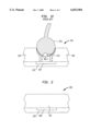
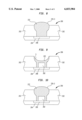
- FIG. 1A represents a cross sectional view of a stacked semiconductor structure 100.
- the stacked semiconductor structure 100 includes a semiconductor substrate 102, an underlying conductive layer 104 overlaid with a layer of insulator 106.
- a plurality of via holes 108 form a conduit between the underlying conductive layer 104 and a bond pad trench 110.
- the bond pad trench 110 is formed by removing a portion of the layer of insulator 106 to a depth AT@ approximating the desired thickness of the bond pad to be formed.
- the metallization layer 112 is placed upon the insulator layer 106 substantially simultaneously filling the via holes 108 and the bond pad trench 110 using a blanket deposition process.
- the metallization layer 112 typically extends above the upper surface of the insulator layer 106 to a predetermined height.
- a portion 112-1 of the metallization layer 112 extending above the upper surface of the insulator layer 106 must be removed so as to expose the insulator layer 106. In this manner, a bond pad is formed of the metal remaining within the bond pad trench 110.
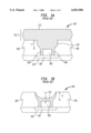
- FIG. 1B is an cross sectional view a bond pad 114 formed by removing the portion 112-1 of the metallization layer 112.
- the portion 112-1 is removed in a process referred to as polishing.
- Polishing removes the portion 112-1 by, for example, physically abrading the metal included in the portion 112-1.
- One such method of abrading the metal included in the portion 112-1 includes using a combination of a rotating pad, or other mechanical device, accompanied by a chemical etch, or slurry.
- the rotating polisher pad typically removes the portion 112-1 of the by a combination of physical abrasion caused by the mechanical action of the polisher and the slurry.
- the rotating polisher pad must be subject to a force applied perpendicular to the insulator layer 106 in order to properly remove the portion 112-1.
- This force causes the rotating polisher pad to flex thereby forming a convex polishing surface.
- the flexing in the rotating polisher pad results in partial removal of the metal deposited within the bond pad trench 110.
- the removal of the metal deposited in the bond pad trench 110 due to the convex shape of the polisher pad in combination with the chemical etch action of the slurry results in a substantial reduction in the bond pad thickness from the thickness T to a thickness T. In some cases the thickness T is of such a magnitude as to expose the insulator 106.
- the reduction of bond bad thickness can result in exposing a portion 106-1 of the insulator layer 106.
- the exposure of the insulator 106 results in poor mechanical and electrical contact with a subsequently attached bond wire.
- the presence of exposed insulator layer 106 can result in the formation of voids 120 between the bond pad 114 and the bond wire 150 as illustrated in FIG. 1C.
- the presence of voids 120 can result in high current densities through the unvoided portions of the bond pad/bond wire junction.
- the high current densities may result in electromigration of the metal included in the bond pad. Electromigration of the bond pad metal may result in long term unacceptable Failure In Time (FIT) rates.
- FIT Failure In Time
- the dual damascene technique should also prevent the formation regions of exposed insulator thereby increasing the probability of poor electrical contact with subsequently placed bond wires.
- the present invention relates to semiconductor devices and more particularly, to an improved method of forming bond pads using a dual damascene etch through a layer stack disposed above a substrate.
- the layer stack includes an underlying conductive layer and an insulating layer disposed above the underlying conductive layer.
- the method includes the following operative steps. At least one via hole is formed in the insulating layer positioned over the underlying device layer and extending to the underlying device layer at the bottom of the via hole.
- a bond pad trench is then formed.
- the bond pad trench substantially takes the form of the desired bond pad.
- a layer of conductive material is then placed over the insulating layer substantially simultaneously filling the via hole and the bond pad trench.
- the bond pad is then formed by removing the layer of conductive material sufficient to expose the upper surface of the insulating layer.
- a method of forming a bond pad in an integrated circuit by performing a dual damascene etch through a layer stack disposed above a substrate includes an underlying device layer, an insulating layer disposed above the underlying device layer.
- the bond pad being suitably disposed to electrically connect the underlying device layer to external circuitry.
- the method includes the following operations. First at least one via hole positioned over the underlying device layer is formed in the insulating layer. The via hole extends to the underlying device layer at the bottom of the via hole. A bond pad trench is then formed in the insulator layer. The bond pad trench substantially takes the form of the bond pad to be formed.
- a layer of conductive material is then placed over the insulating layer substantially simultaneously filling both the via hole and the bond pad trench.
- a layer of polishing resistant material is placed on the conductive layer.
- the bond pad is formed by removing the layer of conductive material sufficient to expose the upper surface of the insulating layer wherein a portion of the layer of conductive material beneath the layer of polishing resistant material is removed at a slower rate than the portion of the layer of conductive material that is not beneath the layer of polishing resistant material.
- FIG. 1A is a cross sectional illustration of a stacked semiconductor structure having a metallization layer deposited on an insulator having a via hole and a bond pad trench formed by conventional dual damascene techniques.
- FIG. 1B is a cross sectional illustration of the stacked semiconductor structure as shown in FIG. 1A showing the subsequent formation of a bond pad.
- FIG. 1C is a cross sectional illustration of the stacked semiconductor structure as shown in FIG. 1B showing an attached bond wire.
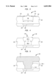
- FIG. 2 is a cross sectional illustration of a stacked semiconductor structure in accordance with an embodiment of the invention.
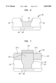
- FIG. 3 is a cross sectional illustration of a stacked semiconductor structure including a via hole in accordance with a basic embodiment of the invention.
- FIG. 4 is a cross sectional illustration of the stacked semiconductor structure as shown in FIG. 3 having a bond pad trench in accordance with an embodiment of the invention.
- FIG. 5 is a cross sectional illustration of a stacked semiconductor structure as shown in FIG. 4 having a metallization layer placed upon a via hole and a bond pad trench in accordance with an embodiment of the invention.
- FIG. 6 is a cross sectional illustration of the stacked semiconductor structure having a bond pad structure formed in accordance with an embodiment of the invention.
- FIG. 7 is a cross sectional illustration of a stacked semiconductor structure having a resistive material layer placed upon a metallization layer in accordance with another embodiment of the invention.
- FIG. 8 is a cross sectional illustration of the stacked semiconductor structure having a bond pad structure formed in accordance with another embodiment of the invention.
- FIG. 9 is a cross sectional illustration of the stacked semiconductor structure having a bond pad structure formed in accordance with yet another embodiment of the invention.
- FIG. 10 is a cross sectional illustration of the stacked semiconductor structure having a bond pad structure formed in accordance with still another embodiment of the invention.
- the invention relates, in one embodiment, to an improved method for forming bond pads in a multi-level coplanar metal/insulator film semiconductor using dual damascene.
- a dual damascene technique is used which incorporates forming a via hole aligned with and substantially the same size as a bond pad trench used to form a bond pad.
- a layer of metallization is placed upon the bond pad trench.
- the bond pad is formed by removing the metallization layer above the upper surface using polishing techniques well known to those skilled in the art. Since the via formed from the via hole is substantially the same size as the bond pad, the concave surface formed in the bond pad structure by the action of the polisher and accompanying slurry does not expose any portions of the insulator layer. In this way, the attaching of a bond wire to the bond pad may be performed without forming voids due to exposed insulator.
- a layer of material capable of reducing the polishing removal rate of metal shielded by the layer of material during the polishing process is place above and aligned with the bond pad trench. In this manner, a portion of metal remains after the surface of the insulator layer has been exposed. The portion of metal eliminates the possibility of forming voids when a bond wire is attached to the bond pad.
- FIG. 2 illustrates a cross sectional view of a stacked semiconductor structure 200 having an insulator layer 202 overlaying a substrate 204 which includes an underlying conductive layer 208 in accordance with one embodiment of the present invention.
- the stacked semiconductor structure 200 may, for example, represent a stacked semiconductor structure employed to fabricate a conventional transistor such as an n FET or p FET (field effect transistor).
- Insulator layer 202 may be deposited on the substrate 204 of a pre-determined conductivity type. Chemical vapor deposition (CVD) or a similar technique may be employed to deposit insulator 202, which typically includes planarized silicon dioxide, such as TEOS, a glass material such as reflowed phosphosilicate glass, or a polymer like polyimide.
- CVD chemical vapor deposition
- insulator layer 202 is formed over previously defined substrate 204, which includes previously defined conductive layer 208.
- the conductive layer 208 may be a portion of an underlying metallization layer.
- the conductive layer 208 may represent a highly doped silicon layer, a conductive metal such as tungsten, or a portion of any type of active device such as, for example, the source or drain region of a transistor.
- the insulator layer 202 may have a thickness in the range of 0.9 micron to about 2.0 microns
- insulator layer 202 has an upper surface 210 upon which a resist layer 212 has been deposited by any technique known to those of ordinary skill in the art.
- the resist layer 212 may have a thickness of about 1000 ⁇ and may be composed of silicon nitride or, in a preferred embodiment, silicon oxynitride.
- the formation of a via hole opening 214 in the resist layer 212 located above the underlying conductive layer 208 is accomplished by conventional photolithographic techniques well known to those skilled in the art. In one embodiment, such a method of forming via hole opening 214 is referred to as reactive ion etching (RIE) utilizing N 2 , O 2 , as well as carbon compounds as an etchant gas.
- RIE reactive ion etching
- ARC organic anti-reflective coating
- ARC organic anti-reflective coating
- use of silicon oxynitride for resist layer 212 eliminates the need for use of ARC.
- the resist layer 212 is composed of silicon oxynitride and no ARC layer is required.
- use of silicon nitride or any other appropriate compound for the resist layer 212 may require the additional step or steps related to ARC deposition and removal.
- a via hole 216 is formed by a first anisotropic etch which removes sufficient insulator material from insulator layer 202 to form the via hole 216.
- the via hole 216 can have a lateral dimension d ranging from approximately 120 microns to approximately 80 microns with a preferred dimension of about 100 microns.
- One such method of removing insulator material is by way of an RIE etch, as described above, using for example, Ar, C 4 F 8 , CO and/or O 2 as reactive gases.
- via hole 216 may have its bottom extend to a point about midway between upper surface 210 and underlying conductive layer 208. In another embodiment, via hole 216 may have its bottom extend to a point substantially near or extending to underlying conductive layer 208.
- a second anisotropic etch may be used to form a bond pad trench 218.
- the bond pad trench 218 substantially takes the form of the bond pad to be formed.
- the bond pad trench 218 therefore has a lateral dimension t ranging from approximately 130 microns to approximately 70 microns with a preferred lateral dimension of about 100 microns.
- the bond pad trench 218 includes a first portion 218-1 and a second portion 218-2.
- the first portion 218-1 extends substantially to the underlying conductive layer 208.
- the second portion 218-2 is arranged to form the desired bond pad.
- the via hole lateral dimension d can be substantially the same size as the bond pad trench lateral dimension t.
- underlying conductive layer 208 may be used as an etch stop whereby the second anisotropic etch process is halted once a pre-determined amount of the constituent material forming the underlying conductive layer 208 is evident in the plasma used in the second anisotropic etch process.
- the overlying metallization layer is ready to be formed by depositing a metal by any appropriate metallization technique.
- Metallization techniques are well known in the art and described, for example in VLSI technology, 2nd Edition, S. M. Sze 1988 McGraw-Hill Publishing Company.
- Suitable metals and alloys for forming the metallization layer include, for example, aluminum, copper, nickel, molybdenum, tungsten, platinum, tantalum disilicide, titanium disilicide, as well as other alloys of these materials.
- Aluminum, aluminum alloys such as aluminum silicon, copper, and tungsten are often the materials of choice for interconnection metallization.
- the metals may be deposited by known techniques such as chemical vapor deposition (CVD), physical vapor deposition (PVD), or low pressure chemical vapor deposition (LPCVD).
- CVD chemical vapor deposition
- PVD physical vapor deposition
- LPCVD low pressure chemical vapor deposition
- Deposition of the metal (usually in blanket fashion over the entire surface of the stacked semiconductor structure 200) fills first portions 218-1 and second portion 218-1 of the bond pad trench 218 thereby substantially simultaneously creating a layer of metal 220 extending above the upper surface 210 of the insulator layer 202 as shown in FIG. 5.
- first and second anisotropic etch is related by the extent that via hole 216 is etched into insulator layer 202. As can be seen, if first anisotropic etch forms extends via hole 216 to a point proximate to the position of underlying conductive layer 208, then the resulting second anisotropic etch will typically be of shorter duration since less insulator material must be etched. This ability to substantially modify the form and structures formed simply by increasing or decreasing the applied etch times offers substantial advantages over more conventional processes.
- FIG. 6 shows a cross sectional view of a bond pad structure 222 formed in accordance with an embodiment of the invention.
- the bond pad structure 222 includes a surface S created by polishing the metal layer 220 as described above.
- the possibility of forming voids is also eliminated when the bond pad structure 222 is electrically connected to a bond wire, for example.
- FIG. 7 shows a metallization layer having a layer of polisher retardant material 230 aligned with and above the bond pad trench 218 in accordance with another embodiment of the invention.
- the layer of polisher retardant material 230 can be dimensioned to approximate the desired size of the bond pad to be formed.
- the layer of polisher retardant material 230 can be formed of SiN, SiON, or Ti, or any other material capable of resisting the polishing action of the polisher and accompanying slurry etch.
- the layer of polisher retardant material 230 provides a temporary shield for the portion 220-2 of the layer of metal 220.
- the action of the polisher/slurry removes the exposed portions 220-1 of the metal layer 220 at a faster rate than the shielded portion 220-2 of layer of metal 220.
- the polisher retardant material 230 is, however, eventually removed by the action of the polisher/slurry. Therefore, a portion 220-3 of the layer of metal 220 remains over the bond pad structure 222 as shown in FIG. 8.
- the portion 220-3 provides an anchor to which subsequent bonding operations may use to attach bond wires, for example.
- the portion 220-3 may be directly bonded to pads included in a flip chip package, for example. In any case, no voids due to the exposure of the insulator layer 202 can be produced due to the presence of the portion 220-3 covering the bond pad structure 222.
- FIG. 9 and FIG. 10 are a cross sectional illustrations of the stacked semiconductor structure 200 having a bond pad structure formed in accordance with other embodiments of the invention.
Abstract
Description
Claims (17)
Priority Applications (5)
| Application Number | Priority Date | Filing Date | Title |
|---|---|---|---|
| US08/997,682 US6033984A (en) | 1997-12-23 | 1997-12-23 | Dual damascene with bond pads |
| EP98120465A EP0926721A3 (en) | 1997-12-23 | 1998-10-29 | Dual damascene with bond pads |
| TW087118611A TW436930B (en) | 1997-12-23 | 1998-11-09 | Dual damascene with bond pads |
| JP10365074A JPH11312704A (en) | 1997-12-23 | 1998-12-22 | Dual damask having bonding pad |
| KR1019980057481A KR19990063359A (en) | 1997-12-23 | 1998-12-23 | Dual Damask Processes with Bonding Pads |
Applications Claiming Priority (1)
| Application Number | Priority Date | Filing Date | Title |
|---|---|---|---|
| US08/997,682 US6033984A (en) | 1997-12-23 | 1997-12-23 | Dual damascene with bond pads |
Publications (1)
| Publication Number | Publication Date |
|---|---|
| US6033984A true US6033984A (en) | 2000-03-07 |
Family
ID=25544264
Family Applications (1)
| Application Number | Title | Priority Date | Filing Date |
|---|---|---|---|
| US08/997,682 Expired - Lifetime US6033984A (en) | 1997-12-23 | 1997-12-23 | Dual damascene with bond pads |
Country Status (5)
| Country | Link |
|---|---|
| US (1) | US6033984A (en) |
| EP (1) | EP0926721A3 (en) |
| JP (1) | JPH11312704A (en) |
| KR (1) | KR19990063359A (en) |
| TW (1) | TW436930B (en) |
Cited By (13)
| Publication number | Priority date | Publication date | Assignee | Title |
|---|---|---|---|---|
| US6090696A (en) * | 1999-10-20 | 2000-07-18 | Taiwan Semicondutor Manufacturing Company | Method to improve the adhesion of a molding compound to a semiconductor chip comprised with copper damascene structures |
| US20010016415A1 (en) * | 1999-11-18 | 2001-08-23 | Taiwan Semiconductor Manufacturing Company | Method of improving copper pad adhesion |
| US6417087B1 (en) * | 1999-12-16 | 2002-07-09 | Agere Systems Guardian Corp. | Process for forming a dual damascene bond pad structure over active circuitry |
| US6551856B1 (en) * | 2000-08-11 | 2003-04-22 | Taiwan Semiconductor Manufacturing Co., Ltd. | Method for forming copper pad redistribution and device formed |
| US20040198035A1 (en) * | 2003-04-03 | 2004-10-07 | Chao-Cheng Chen | Method of damascene process flow |
| US6838769B1 (en) | 1999-12-16 | 2005-01-04 | Agere Systems Inc. | Dual damascene bond pad structure for lowering stress and allowing circuitry under pads |
| US20050156332A1 (en) * | 1998-01-23 | 2005-07-21 | Koji Yamamoto | Damascene interconnection and semiconductor device |
| US20060071304A1 (en) * | 2004-09-29 | 2006-04-06 | International Business Machines Corporation | Structure and layout of a fet prime cell |
| US20060211167A1 (en) * | 2005-03-18 | 2006-09-21 | International Business Machines Corporation | Methods and systems for improving microelectronic i/o current capabilities |
| US20080272466A1 (en) * | 2005-06-28 | 2008-11-06 | Micron Technology, Inc. | Semiconductor substrates including vias of nonuniform cross section and associated structures |
| US20110156260A1 (en) * | 2009-12-28 | 2011-06-30 | Yu-Hua Huang | Pad structure and integrated circuit chip with such pad structure |
| US20120273937A1 (en) * | 2011-04-30 | 2012-11-01 | Stats Chippac, Ltd. | Semiconductor Device and Method of Forming Bump Interconnect Structure with Conductive Layer Over Buffer Layer |
| US20130133919A1 (en) * | 2011-11-28 | 2013-05-30 | International Business Machines Corporation | Top corner rounding of damascene wire for insulator crack suppression |
Families Citing this family (1)
| Publication number | Priority date | Publication date | Assignee | Title |
|---|---|---|---|---|
| GB2364170B (en) * | 1999-12-16 | 2002-06-12 | Lucent Technologies Inc | Dual damascene bond pad structure for lowering stress and allowing circuitry under pads and a process to form the same |
Citations (7)
| Publication number | Priority date | Publication date | Assignee | Title |
|---|---|---|---|---|
| US4057659A (en) * | 1974-06-12 | 1977-11-08 | Siemens Aktiengesellschaft | Semiconductor device and a method of producing such device |
| US5534460A (en) * | 1995-04-27 | 1996-07-09 | Vanguard International Semiconductor Corp. | Optimized contact plug process |
| US5578523A (en) * | 1995-02-24 | 1996-11-26 | Motorola, Inc. | Method for forming inlaid interconnects in a semiconductor device |
| US5739563A (en) * | 1995-03-15 | 1998-04-14 | Kabushiki Kaisha Toshiba | Ferroelectric type semiconductor device having a barium titanate type dielectric film and method for manufacturing the same |
| US5773363A (en) * | 1994-11-08 | 1998-06-30 | Micron Technology, Inc. | Semiconductor processing method of making electrical contact to a node |
| US5780337A (en) * | 1996-09-23 | 1998-07-14 | United Microelectronics Corporation | Method of fabricating a bit line of a dynamic random access memory |
| US5877076A (en) * | 1997-10-14 | 1999-03-02 | Industrial Technology Research Institute | Opposed two-layered photoresist process for dual damascene patterning |
Family Cites Families (5)
| Publication number | Priority date | Publication date | Assignee | Title |
|---|---|---|---|---|
| JPS5561027A (en) * | 1978-10-30 | 1980-05-08 | Chiyou Lsi Gijutsu Kenkyu Kumiai | Gas plasma etching |
| US5266446A (en) * | 1990-11-15 | 1993-11-30 | International Business Machines Corporation | Method of making a multilayer thin film structure |
| US5618381A (en) * | 1992-01-24 | 1997-04-08 | Micron Technology, Inc. | Multiple step method of chemical-mechanical polishing which minimizes dishing |
| US5516710A (en) * | 1994-11-10 | 1996-05-14 | Northern Telecom Limited | Method of forming a transistor |
| JP2728025B2 (en) * | 1995-04-13 | 1998-03-18 | 日本電気株式会社 | Method for manufacturing semiconductor device |
-
1997
- 1997-12-23 US US08/997,682 patent/US6033984A/en not_active Expired - Lifetime
-
1998
- 1998-10-29 EP EP98120465A patent/EP0926721A3/en not_active Withdrawn
- 1998-11-09 TW TW087118611A patent/TW436930B/en not_active IP Right Cessation
- 1998-12-22 JP JP10365074A patent/JPH11312704A/en active Pending
- 1998-12-23 KR KR1019980057481A patent/KR19990063359A/en not_active Application Discontinuation
Patent Citations (7)
| Publication number | Priority date | Publication date | Assignee | Title |
|---|---|---|---|---|
| US4057659A (en) * | 1974-06-12 | 1977-11-08 | Siemens Aktiengesellschaft | Semiconductor device and a method of producing such device |
| US5773363A (en) * | 1994-11-08 | 1998-06-30 | Micron Technology, Inc. | Semiconductor processing method of making electrical contact to a node |
| US5578523A (en) * | 1995-02-24 | 1996-11-26 | Motorola, Inc. | Method for forming inlaid interconnects in a semiconductor device |
| US5739563A (en) * | 1995-03-15 | 1998-04-14 | Kabushiki Kaisha Toshiba | Ferroelectric type semiconductor device having a barium titanate type dielectric film and method for manufacturing the same |
| US5534460A (en) * | 1995-04-27 | 1996-07-09 | Vanguard International Semiconductor Corp. | Optimized contact plug process |
| US5780337A (en) * | 1996-09-23 | 1998-07-14 | United Microelectronics Corporation | Method of fabricating a bit line of a dynamic random access memory |
| US5877076A (en) * | 1997-10-14 | 1999-03-02 | Industrial Technology Research Institute | Opposed two-layered photoresist process for dual damascene patterning |
Cited By (21)
| Publication number | Priority date | Publication date | Assignee | Title |
|---|---|---|---|---|
| US7042100B2 (en) * | 1998-01-23 | 2006-05-09 | Rohm Co., Ltd | Damascene interconnection and semiconductor device |
| US20050156332A1 (en) * | 1998-01-23 | 2005-07-21 | Koji Yamamoto | Damascene interconnection and semiconductor device |
| US6090696A (en) * | 1999-10-20 | 2000-07-18 | Taiwan Semicondutor Manufacturing Company | Method to improve the adhesion of a molding compound to a semiconductor chip comprised with copper damascene structures |
| US20010016415A1 (en) * | 1999-11-18 | 2001-08-23 | Taiwan Semiconductor Manufacturing Company | Method of improving copper pad adhesion |
| US7026721B2 (en) * | 1999-11-18 | 2006-04-11 | Taiwan Semiconductor Manufacturing Company, Ltd. | Method of improving copper pad adhesion |
| US6838769B1 (en) | 1999-12-16 | 2005-01-04 | Agere Systems Inc. | Dual damascene bond pad structure for lowering stress and allowing circuitry under pads |
| US6417087B1 (en) * | 1999-12-16 | 2002-07-09 | Agere Systems Guardian Corp. | Process for forming a dual damascene bond pad structure over active circuitry |
| US6551856B1 (en) * | 2000-08-11 | 2003-04-22 | Taiwan Semiconductor Manufacturing Co., Ltd. | Method for forming copper pad redistribution and device formed |
| US6960496B2 (en) | 2003-04-03 | 2005-11-01 | Taiwan Semiconductor Manufacturing | Method of damascene process flow |
| US20040198035A1 (en) * | 2003-04-03 | 2004-10-07 | Chao-Cheng Chen | Method of damascene process flow |
| US20080076212A1 (en) * | 2004-09-29 | 2008-03-27 | International Business Machines Corporation | Structure and layout of a fet prime cell |
| US20060071304A1 (en) * | 2004-09-29 | 2006-04-06 | International Business Machines Corporation | Structure and layout of a fet prime cell |
| US8187930B2 (en) | 2004-09-29 | 2012-05-29 | International Business Machines Corporation | Structure and layout of a FET prime cell |
| US8829572B2 (en) | 2004-09-29 | 2014-09-09 | International Business Machines Corporation | Structure and layout of a FET prime cell |
| US20060211167A1 (en) * | 2005-03-18 | 2006-09-21 | International Business Machines Corporation | Methods and systems for improving microelectronic i/o current capabilities |
| US20080272466A1 (en) * | 2005-06-28 | 2008-11-06 | Micron Technology, Inc. | Semiconductor substrates including vias of nonuniform cross section and associated structures |
| US7687916B2 (en) * | 2005-06-28 | 2010-03-30 | Micron Technology, Inc. | Semiconductor substrates including vias of nonuniform cross-section and associated structures |
| US20110156260A1 (en) * | 2009-12-28 | 2011-06-30 | Yu-Hua Huang | Pad structure and integrated circuit chip with such pad structure |
| US20120273937A1 (en) * | 2011-04-30 | 2012-11-01 | Stats Chippac, Ltd. | Semiconductor Device and Method of Forming Bump Interconnect Structure with Conductive Layer Over Buffer Layer |
| US20130133919A1 (en) * | 2011-11-28 | 2013-05-30 | International Business Machines Corporation | Top corner rounding of damascene wire for insulator crack suppression |
| US8575022B2 (en) * | 2011-11-28 | 2013-11-05 | International Business Machines Corporation | Top corner rounding of damascene wire for insulator crack suppression |
Also Published As
| Publication number | Publication date |
|---|---|
| EP0926721A2 (en) | 1999-06-30 |
| EP0926721A3 (en) | 2001-12-19 |
| JPH11312704A (en) | 1999-11-09 |
| KR19990063359A (en) | 1999-07-26 |
| TW436930B (en) | 2001-05-28 |
Similar Documents
| Publication | Publication Date | Title |
|---|---|---|
| US6103629A (en) | Self-aligned interconnect using high selectivity metal pillars and a via exclusion mask | |
| US6333559B1 (en) | Method/structure for creating aluminum wirebound pad on copper BEOL | |
| US7528064B2 (en) | Interconnect structures with bond-pads and methods of forming bump sites on bond-pads | |
| US7741698B2 (en) | Post last wiring level inductor using patterned plate process | |
| US6383920B1 (en) | Process of enclosing via for improved reliability in dual damascene interconnects | |
| US8901733B2 (en) | Reliable metal bumps on top of I/O pads after removal of test probe marks | |
| US20030020163A1 (en) | Bonding pad structure for copper/low-k dielectric material BEOL process | |
| US6265313B1 (en) | Method of manufacturing copper interconnect | |
| JP5739434B2 (en) | Semiconductor device having copper plug and method for forming the device | |
| US6638867B2 (en) | Method for forming a top interconnection level and bonding pads on an integrated circuit chip | |
| US6033984A (en) | Dual damascene with bond pads | |
| US7763537B2 (en) | Metal interconnection of semiconductor device and method for forming the same | |
| US20020064929A1 (en) | Novel passivation structure and its method of fabrication | |
| US6348734B1 (en) | Self-aligned copper interconnect architecture with enhanced copper diffusion barrier | |
| US6156642A (en) | Method of fabricating a dual damascene structure in an integrated circuit | |
| US10361119B1 (en) | Enlarged contact area structure using noble metal cap and noble metal liner | |
| GB2364170A (en) | Dual damascene bond pad structure for lowering stress and allowing circuitry under pads | |
| US20030178644A1 (en) | Reinforced bond-pad substructure and method for fabricating the same | |
| US6873047B2 (en) | Semiconductor device and manufacturing method thereof | |
| US6583054B2 (en) | Method for forming conductive line in semiconductor device | |
| JP3415081B2 (en) | Semiconductor device and method of manufacturing semiconductor device | |
| US6396151B1 (en) | Partially-overlapped interconnect structure and method of making | |
| KR100834283B1 (en) | The making method of metal line | |
| JP2004503089A6 (en) | Via-first dual damascene method for copper metallization | |
| JP2004503089A (en) | Via-first dual damascene method for copper metallization |
Legal Events
| Date | Code | Title | Description |
|---|---|---|---|
| AS | Assignment |
Owner name: SIEMENS MICROELECTRONICS, INC., CALIFORNIA Free format text: ASSIGNMENT OF ASSIGNORS INTEREST;ASSIGNORS:SCHNABEL, RAINER FLORIAN;NING, XIAN J.;SPULER, BRUNO;REEL/FRAME:009219/0087;SIGNING DATES FROM 19980417 TO 19980421 |
|
| AS | Assignment |
Owner name: SIEMENS AKTIENGESELLSCHAFT, GERMANY Free format text: ASSIGNMENT OF ASSIGNORS INTEREST;ASSIGNOR:SIEMENS MICROELECTRONICS, INC.;REEL/FRAME:009378/0057 Effective date: 19980724 |
|
| STCF | Information on status: patent grant |
Free format text: PATENTED CASE |
|
| FEPP | Fee payment procedure |
Free format text: PAYOR NUMBER ASSIGNED (ORIGINAL EVENT CODE: ASPN); ENTITY STATUS OF PATENT OWNER: LARGE ENTITY |
|
| FPAY | Fee payment |
Year of fee payment: 4 |
|
| FPAY | Fee payment |
Year of fee payment: 8 |
|
| AS | Assignment |
Owner name: INFINEON TECHNOLOGIES AG,GERMANY Free format text: ASSIGNMENT OF ASSIGNORS INTEREST;ASSIGNOR:SIEMENS AKTIENGESELLSCHAFT;REEL/FRAME:024120/0001 Effective date: 19990331 |
|
| AS | Assignment |
Owner name: QIMONDA AG,GERMANY Free format text: ASSIGNMENT OF ASSIGNORS INTEREST;ASSIGNOR:INFINEON TECHNOLOGIES AG;REEL/FRAME:024195/0054 Effective date: 20060425 |
|
| FPAY | Fee payment |
Year of fee payment: 12 |
|
| AS | Assignment |
Owner name: INFINEON TECHNOLOGIES AG, GERMANY Free format text: ASSIGNMENT OF ASSIGNORS INTEREST;ASSIGNOR:QIMONDA AG;REEL/FRAME:035623/0001 Effective date: 20141009 |
|
| AS | Assignment |
Owner name: POLARIS INNOVATIONS LIMITED, IRELAND Free format text: ASSIGNMENT OF ASSIGNORS INTEREST;ASSIGNOR:INFINEON TECHNOLOGIES AG;REEL/FRAME:036305/0890 Effective date: 20150708 |