US6033916A - Measuring device and method for making same - Google Patents
Measuring device and method for making same Download PDFInfo
- Publication number
- US6033916A US6033916A US08/785,630 US78563097A US6033916A US 6033916 A US6033916 A US 6033916A US 78563097 A US78563097 A US 78563097A US 6033916 A US6033916 A US 6033916A
- Authority
- US
- United States
- Prior art keywords
- contact surface
- sensor
- process according
- structuring
- active contact
- Prior art date
- Legal status (The legal status is an assumption and is not a legal conclusion. Google has not performed a legal analysis and makes no representation as to the accuracy of the status listed.)
- Expired - Fee Related
Links
Images
Classifications
-
- G—PHYSICS
- G01—MEASURING; TESTING
- G01N—INVESTIGATING OR ANALYSING MATERIALS BY DETERMINING THEIR CHEMICAL OR PHYSICAL PROPERTIES
- G01N27/00—Investigating or analysing materials by the use of electric, electrochemical, or magnetic means
- G01N27/26—Investigating or analysing materials by the use of electric, electrochemical, or magnetic means by investigating electrochemical variables; by using electrolysis or electrophoresis
- G01N27/403—Cells and electrode assemblies
- G01N27/414—Ion-sensitive or chemical field-effect transistors, i.e. ISFETS or CHEMFETS
- G01N27/4145—Ion-sensitive or chemical field-effect transistors, i.e. ISFETS or CHEMFETS specially adapted for biomolecules, e.g. gate electrode with immobilised receptors
-
- H—ELECTRICITY
- H01—ELECTRIC ELEMENTS
- H01L—SEMICONDUCTOR DEVICES NOT COVERED BY CLASS H10
- H01L2924/00—Indexing scheme for arrangements or methods for connecting or disconnecting semiconductor or solid-state bodies as covered by H01L24/00
- H01L2924/0001—Technical content checked by a classifier
- H01L2924/0002—Not covered by any one of groups H01L24/00, H01L24/00 and H01L2224/00
-
- Y—GENERAL TAGGING OF NEW TECHNOLOGICAL DEVELOPMENTS; GENERAL TAGGING OF CROSS-SECTIONAL TECHNOLOGIES SPANNING OVER SEVERAL SECTIONS OF THE IPC; TECHNICAL SUBJECTS COVERED BY FORMER USPC CROSS-REFERENCE ART COLLECTIONS [XRACs] AND DIGESTS
- Y10—TECHNICAL SUBJECTS COVERED BY FORMER USPC
- Y10S—TECHNICAL SUBJECTS COVERED BY FORMER USPC CROSS-REFERENCE ART COLLECTIONS [XRACs] AND DIGESTS
- Y10S436/00—Chemistry: analytical and immunological testing
- Y10S436/805—Optical property
Definitions
- the invention pertains to a process for producing a device for measuring or investigating physiological parameters in biological components ("biocomponents").
- the device has at least one sensor having a measuring structure with an active contact surface for the biological components.
- the invention relates to a measuring device produced according to the process.
- Biosensors continue to gain in importance with the very large number of cellular microsystems.
- the combination of a biological microsystem with a physical transducer permits the conversion of primary signal responses of the biological system into an electrical signal, which can then be registered and processed further without difficulty.
- the primary sensory function of the system is assumed by a living cell or its components (e.g., receptors, gamma-globulins), and that their output signals are received by different, physical transducers.
- the object of the present invention is to increase the mechanical anchoring of biocomponents (e.g., cells, receptors, gamma globulins) on the active contact surfaces of the sensors and further to improve the signal transmission properties and measurement sensitivity further.
- biocomponents e.g., cells, receptors, gamma globulins
- the active contact surface of the sensor be structured approximately corresponding to the outer contours of the biocomponent in question.
- the biocomponents e.g., cells, biological molecules, parts of cells and the like
- the sensor can be maintained operative for a longer period of time with living cells or the like.
- the shape of the biocomponents is preferably incorporated by means of a replica technique, and if the contact surface coating is provided with a complementary reverse structuring corresponding approximately to the shape of the biocomponents especially by means of a plasma bombarding technique or etching technique.
- a direct adaptation of the surface structure or profiling to the topography of the biological systems or the biocomponents to be deposited consequently takes place, by means of which an especially good anchoring is assured.
- the transfer of the topography of the biocomponents to the active contact surface can take place with a known replica technique.
- a modified form of the process provides that material particles for cluster formation, preferably comprising about 12,000 atoms with a kinetic energy smaller than about 1 eV/atom, are bombarded or sputtered onto the active contact surface for the formation of a contact surface coating with a loose structure or gaps.
- An anchoring layer can thereby be built up on the contact surface of the sensor so that it which has a comparatively loose, porous structure. Gaps or holes are thereby formed in which, for example, immune receptors can be anchored. These biocomponents are very well anchored by interlocking, and the sensors thereby manifest a much better long term stability. At the same time, one also obtains an essentially greater measurement sensitivity, as the distance between the biocomponents and sensor contact surface is at least diminished, and the charge transfer process, which influences the sensor, consequently transpires closer to the sensor.
- the measuring device produced according to the process of the invention is characterized in that the active contact surface of the sensors has a surface topography approximately adapted to the shape of the biocomponent to be examined.
- the surface topography of the sensor contact surface is basically a complementary reverse structuring of the biocomponent in question.
- the senor has a field effect transistor with a contact surface coating, preferably of aluminum oxide, silicon nitride or similar structuring material.
- a contact surface coating preferably of aluminum oxide, silicon nitride or similar structuring material.
- aluminum oxide or silicon nitride has the advantage that roughened surfaces fitting the structure of the biocomponents can also be created with them.
- Aluminum oxide has a high pH sensitivity and a high sensitivity toward physiological signals, and improves the electrical coupling of a cell or similar biocomponent to the field effect transistor and consequently increases its output signal.
- Silicon nitride has a high voltage sensitivity.
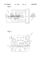
- FIG. 1 is a schematic representation of a biomedical sensor system with various sensors
- FIG. 2 is a schematic representation of an FET sensor
- FIG. 3 is a schematic representation of an FET sensor with coating and deposited immune receptors.
- a biomedical sensor system 1 depicted in FIG. 1 has a miniaturized chamber 2 for accommodation of cells to be examined, whose function is to be investigated by various discrete sensors 5. These sensors are connected with a sensor activation and signal preprocessing facility 3, which for its part is connected with a computer 4 for gathering measurement data and for evaluation, as well as for controlling the course of measurement and temperature regulation.
- optical sensors 5a, an oxygen sensor 5b, temperature sensors 5c, as well as cell potential measurement sensors 5d, interdigital structures 5e for impedance measurements, and if needed, external sensors 5f are also used in addition to sensors 5 with a field effect transistor structure.
- a microscope 7 is also indicated in connection with the area of observation 6 of the sensor system 1.
- Designated by 8 is a function block for medium, test substances, pumps and the like. This function block as well as the sensors are connected with the sensor control and signal preprocessing facility 3.
- the microsensors have the most varied geometies but are always so constructed, such that either living cells are situated in their immediate vicinity, and/or the cells are an integral component part of the microsensor.
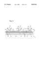
- FIG. 2 shows an individual FET sensor 5 which has a field effect transistor 9 which reacts very sensitively to electric fields.
- This field effect transistor 9 has a silicon substrate 21 into which highly doped zones 22, 23 for drain and source are diffused with the conduction type opposed to the substrate.
- a silicon oxide layer 12 is situated as a dielectric which forms an active sensor contact layer on the exterior, by which the FET can be controlled.
- a drop of nutrient solution 10 with the cells 11 contained in it is situated on the silicon oxide layer 12. Every cell 11 carries different receptors 13 on its membrane. Suitable messenger substances 14, which can anchor themselves on the cells by the respective receptors adapted thereto, swim to the receptors in the nutrient solution 10. This leads to induced changes in molecular bonds and shifts in electric charges. The thus induced change in electric parameters is detected by the field effect transistor 9 and converted into an electric signal. An electrical transmission thereby arises from a biological signal transmission. This can then be amplified without difficulty and electrically read out and processed further for diagnostic purposes.
- the active contact surface 24 of the FET sensor is structured and thereby adapted to the exterior cell structure.
- the cells themselves are comparitively sharply structured and have many indentations and bulges.
- the external structuring of the active contact surface 24 is depicted greatly enlarged in FIG. 3 for clarification.
- the coating 15 of the active contact surface of the sensor 5 is recognizable here. It consists here of deposited aluminum oxide clusters 16, which are indicated by round circles. An intensive beam can be produced in a vacuum from such clusters. If one bombards or sputters these against a surface, a different structure results according to the energy of the beam.
- the clusters form a composite whose structure depends, among other things, upon the energy with which it is applied to the dielectric layer 12 of the field effect transistor 9.
- the kinetic energy of the bombarding cluster amounts to approximately 1 eV/atom.
- About 5000 atoms are thereby deposited in a cluster in any given case, whereby each cluster has a diameter of about 10 nanometers.
- the deposited clusters 16 are then oxidized and tempered, which leads to a porous but hard aluminum oxide layer.
- the aluminum oxide layer can be processed by various techniques (e.g., plasma bombardment technique, etching), so that cracks and gaps 17 arise.
- immune receptors 18 e.g., gamma-globulin, a Y-shaped biological molecule
- immune receptors 18 can, for example, be particularly well directly anchored in the holes thus arising, which can have a diameter of about 10 nm. Since now the charge transfer process, which influences the FET transpires much closer to the FET, because the intermediate function of the cell itself is switched off, an essentially higher electrical signal is to be expected. The measurement sensitivity is thereby correspondingly improved.
- Silicon nitride can be used instead of aluminum oxide as a structuring material.
- the structuring material used in any given case is guided by the relevant requirements for the measuring procedure in question.
- silicon nitride is used when an increased voltage sensitivity is needed, while aluminum oxide is used when the requirements for pH sensitivity are great.
- the immune receptors 18 are formed by Y-shaped biological molecules., which engage directly into the porous, ceramic structure with their support region 19, with which they normally stick in the cell wall, whereby they are very well anchored and whereby the sensors generally have a much better long term stability.
- the two sensorially sensitive ends 20 of the immune receptors 18 protrude outwardly from the coating 15.
- the anchoring of the immune receptors 18 in the coating 15 can take place by a sedimentation process with subsequent rinsing stages.
Abstract
Description
Claims (7)
Priority Applications (1)
| Application Number | Priority Date | Filing Date | Title |
|---|---|---|---|
| US09/468,449 US6210977B1 (en) | 1996-01-17 | 1999-12-21 | Measuring device and method for making same |
Applications Claiming Priority (2)
| Application Number | Priority Date | Filing Date | Title |
|---|---|---|---|
| DE19601488A DE19601488C1 (en) | 1996-01-17 | 1996-01-17 | Measuring device manufacturing method for measuring or testing physiological parameter at biocomponent |
| DE19601488 | 1996-01-17 |
Related Child Applications (1)
| Application Number | Title | Priority Date | Filing Date |
|---|---|---|---|
| US09/468,449 Division US6210977B1 (en) | 1996-01-17 | 1999-12-21 | Measuring device and method for making same |
Publications (1)
| Publication Number | Publication Date |
|---|---|
| US6033916A true US6033916A (en) | 2000-03-07 |
Family
ID=7782959
Family Applications (2)
| Application Number | Title | Priority Date | Filing Date |
|---|---|---|---|
| US08/785,630 Expired - Fee Related US6033916A (en) | 1996-01-17 | 1997-01-17 | Measuring device and method for making same |
| US09/468,449 Expired - Fee Related US6210977B1 (en) | 1996-01-17 | 1999-12-21 | Measuring device and method for making same |
Family Applications After (1)
| Application Number | Title | Priority Date | Filing Date |
|---|---|---|---|
| US09/468,449 Expired - Fee Related US6210977B1 (en) | 1996-01-17 | 1999-12-21 | Measuring device and method for making same |
Country Status (4)
| Country | Link |
|---|---|
| US (2) | US6033916A (en) |
| EP (1) | EP0785424B1 (en) |
| JP (1) | JP4005657B2 (en) |
| DE (2) | DE19601488C1 (en) |
Cited By (22)
| Publication number | Priority date | Publication date | Assignee | Title |
|---|---|---|---|---|
| US6245057B1 (en) * | 1997-04-23 | 2001-06-12 | Micronas Intermetall Gmbh | Device for treating malignant, tumorous tissue areas |
| US6315940B1 (en) * | 1996-11-16 | 2001-11-13 | Nmi Naturwissenschaftliches Und Medizinisches Institut An Der Universitat Tubingen In Reutlingen | Microelement device |
| US6325904B1 (en) | 1997-11-12 | 2001-12-04 | Protiveris, Inc. | Nanoelectrode arrays |
| DE10028257A1 (en) * | 2000-06-09 | 2001-12-20 | Alpha Technology Ges Fuer Ange | Analysis chip used e.g. in DNA sequencing, comprises baseplate carrying array of electronically-addressable points, with matching perforated plate attached to it |
| WO2002004935A1 (en) * | 2000-07-06 | 2002-01-17 | Asahi Kasei Kabushiki Kaisha | Molecule detecting sensor |
| US20020014408A1 (en) * | 2000-08-04 | 2002-02-07 | Schroeder Kirk S. | System for rapid chemical activation in high-throughput electrophysiological measurements |
| US6413474B1 (en) * | 1998-11-17 | 2002-07-02 | Micronas Gmbh | Measuring device |
| DE10102063A1 (en) * | 2001-01-17 | 2002-07-25 | Alpha Technology Ges Fuer Ange | Analysis chip, e.g. for genetic analysis, has layer comprising grid of electrically connected spots and second layer comprising conductive structure of rings connected by strips, where layers are separated by insulating layers |
| US20020104757A1 (en) * | 1997-12-17 | 2002-08-08 | Christian Schmidt | Efficient methods for the analysis of ion channel proteins |
| US20030008412A1 (en) * | 1997-10-10 | 2003-01-09 | Ciphergen Biosystems, Inc. | Plate alignment and sample transfer indicia for a multiwell multiplate stack and method for processing biological/chemical samples using the same |
| US20030052002A1 (en) * | 1997-12-17 | 2003-03-20 | Horst Vogel | Multiaperture sample positioning and analysis system |
| US20030098248A1 (en) * | 1997-12-17 | 2003-05-29 | Horst Vogel | Multiaperture sample positioning and analysis system |
| US6656678B1 (en) * | 1997-12-04 | 2003-12-02 | Micronas Gmbh | Method for examination of a surface layer |
| US20060228723A1 (en) * | 2002-01-16 | 2006-10-12 | Keith Bradley | System and method for electronic sensing of biomolecules |
| US20070132043A1 (en) * | 2002-01-16 | 2007-06-14 | Keith Bradley | Nano-electronic sensors for chemical and biological analytes, including capacitance and bio-membrane devices |
| US20070178477A1 (en) * | 2002-01-16 | 2007-08-02 | Nanomix, Inc. | Nanotube sensor devices for DNA detection |
| US7270730B2 (en) | 2000-08-04 | 2007-09-18 | Essen Instruments, Inc. | High-throughput electrophysiological measurement system |
| CN100516861C (en) * | 2004-03-02 | 2009-07-22 | 迈克纳斯公司 | Field effect transistor for measuring biocomponents |
| US20100085067A1 (en) * | 2002-09-05 | 2010-04-08 | Nanomix, Inc. | Anesthesia monitor, capacitance nanosensors and dynamic sensor sampling method |
| US20100283835A1 (en) * | 2007-01-11 | 2010-11-11 | Joerg Bewersdorf | Microscopic imaging techniques |
| US8741581B2 (en) | 2009-04-27 | 2014-06-03 | Technion Research And Development Foundation Ltd. | Markers for cancer detection |
| US8993346B2 (en) | 2009-08-07 | 2015-03-31 | Nanomix, Inc. | Magnetic carbon nanotube based biodetection |
Families Citing this family (12)
| Publication number | Priority date | Publication date | Assignee | Title |
|---|---|---|---|---|
| DE19753790C2 (en) * | 1997-12-04 | 2001-07-19 | Micronas Gmbh | Method for examining a surface layer |
| DE10018433C2 (en) * | 2000-04-14 | 2003-04-03 | Inst Zelltechnologie E V | Sensor system for determining the pollution in water, this comprehensive device, process for its production and its use |
| US20020165675A1 (en) * | 2001-03-03 | 2002-11-07 | Golovlev Valeri V. | Method and microelectronic device for multi-site molecule detection |
| US20050266455A1 (en) * | 2002-03-02 | 2005-12-01 | Sci Tec, Inc. | Method and microelectronic device for multi-site molecule detection |
| AU2003234315A1 (en) * | 2002-04-30 | 2003-11-17 | William R. Moyle | Sensors for biomolecular detection and cell classification |
| JP4438049B2 (en) | 2003-08-11 | 2010-03-24 | キヤノン株式会社 | Field effect transistor, sensor using the same, and manufacturing method thereof |
| US8198658B2 (en) * | 2007-06-13 | 2012-06-12 | Samsung Electronics Co., Ltd. | Device and method for detecting biomolecules using adsorptive medium and field effect transistor |
| KR101465961B1 (en) * | 2007-10-09 | 2014-12-01 | 삼성전자주식회사 | A method and a device for detecting DNAs, etc. |
| US7772569B2 (en) * | 2008-04-01 | 2010-08-10 | The Jackson Laboratory | 3D biplane microscopy |
| JP5517125B2 (en) * | 2010-02-05 | 2014-06-11 | 国立大学法人 東京大学 | Cell measuring device |
| JP5445778B2 (en) * | 2010-08-27 | 2014-03-19 | 大日本印刷株式会社 | Current mirror type biosensor and method of manufacturing current mirror type biosensor |
| JP5413607B2 (en) * | 2010-08-27 | 2014-02-12 | 大日本印刷株式会社 | Current mirror biosensor |
Citations (11)
| Publication number | Priority date | Publication date | Assignee | Title |
|---|---|---|---|---|
| US3926564A (en) * | 1974-02-25 | 1975-12-16 | Gen Electric | Substrate for immunological tests and method of fabrication thereof |
| US4090849A (en) * | 1976-12-20 | 1978-05-23 | General Electric Company | Diagnostic device and manufacture thereof |
| DE2947050A1 (en) * | 1979-11-22 | 1981-05-27 | Karoly Dr. 4600 Dortmund Dobos | Ion, atom, or molecule sensor - with bipolar transistor with perforated gate as sensor |
| US4334880A (en) * | 1980-10-20 | 1982-06-15 | Malmros Mark K | Analytical device having semiconductive polyacetylene element associated with analyte-binding substance |
| US4777019A (en) * | 1985-04-12 | 1988-10-11 | Thomas Dandekar | Biosensor |
| WO1988009499A1 (en) * | 1987-05-18 | 1988-12-01 | The Johns Hopkins University | Optimized capacitive sensor for chemical analysis and measurement |
| US4820649A (en) * | 1986-09-22 | 1989-04-11 | Teijin Limited | Method and kit having layered device for detecting biological component by interference color |
| US5124172A (en) * | 1989-04-28 | 1992-06-23 | Alcan International Limited | Thin film diagnostic device |
| US5418136A (en) * | 1991-10-01 | 1995-05-23 | Biostar, Inc. | Devices for detection of an analyte based upon light interference |
| US5496701A (en) * | 1991-06-04 | 1996-03-05 | Fisons Plc | Optical biosensor method for determining an analyte |
| DE19512117A1 (en) * | 1995-04-04 | 1996-10-10 | Itt Ind Gmbh Deutsche | Measuring device |
-
1996
- 1996-01-17 DE DE19601488A patent/DE19601488C1/en not_active Expired - Fee Related
-
1997
- 1997-01-08 DE DE59703324T patent/DE59703324D1/en not_active Expired - Lifetime
- 1997-01-08 EP EP97100160A patent/EP0785424B1/en not_active Expired - Lifetime
- 1997-01-13 JP JP00362997A patent/JP4005657B2/en not_active Expired - Fee Related
- 1997-01-17 US US08/785,630 patent/US6033916A/en not_active Expired - Fee Related
-
1999
- 1999-12-21 US US09/468,449 patent/US6210977B1/en not_active Expired - Fee Related
Patent Citations (11)
| Publication number | Priority date | Publication date | Assignee | Title |
|---|---|---|---|---|
| US3926564A (en) * | 1974-02-25 | 1975-12-16 | Gen Electric | Substrate for immunological tests and method of fabrication thereof |
| US4090849A (en) * | 1976-12-20 | 1978-05-23 | General Electric Company | Diagnostic device and manufacture thereof |
| DE2947050A1 (en) * | 1979-11-22 | 1981-05-27 | Karoly Dr. 4600 Dortmund Dobos | Ion, atom, or molecule sensor - with bipolar transistor with perforated gate as sensor |
| US4334880A (en) * | 1980-10-20 | 1982-06-15 | Malmros Mark K | Analytical device having semiconductive polyacetylene element associated with analyte-binding substance |
| US4777019A (en) * | 1985-04-12 | 1988-10-11 | Thomas Dandekar | Biosensor |
| US4820649A (en) * | 1986-09-22 | 1989-04-11 | Teijin Limited | Method and kit having layered device for detecting biological component by interference color |
| WO1988009499A1 (en) * | 1987-05-18 | 1988-12-01 | The Johns Hopkins University | Optimized capacitive sensor for chemical analysis and measurement |
| US5124172A (en) * | 1989-04-28 | 1992-06-23 | Alcan International Limited | Thin film diagnostic device |
| US5496701A (en) * | 1991-06-04 | 1996-03-05 | Fisons Plc | Optical biosensor method for determining an analyte |
| US5418136A (en) * | 1991-10-01 | 1995-05-23 | Biostar, Inc. | Devices for detection of an analyte based upon light interference |
| DE19512117A1 (en) * | 1995-04-04 | 1996-10-10 | Itt Ind Gmbh Deutsche | Measuring device |
Non-Patent Citations (2)
| Title |
|---|
| N. Jaffrezic Renault and C. Martelet, Preparation of well engineered thin molecular layers on semiconductor based transducers Sensors and Actuators A Physical A 32, (1992), pp. 307 312. * |
| N. Jaffrezic-Renault and C. Martelet, "Preparation of well-engineered thin molecular layers on semiconductor-based transducers" Sensors and Actuators--A Physical A 32, (1992), pp. 307-312. |
Cited By (37)
| Publication number | Priority date | Publication date | Assignee | Title |
|---|---|---|---|---|
| US6315940B1 (en) * | 1996-11-16 | 2001-11-13 | Nmi Naturwissenschaftliches Und Medizinisches Institut An Der Universitat Tubingen In Reutlingen | Microelement device |
| US6989089B2 (en) | 1996-11-16 | 2006-01-24 | Nmi Naturwissenschaftliches Und Medizinisches Institut An Der Universitat Tubingen In Reutlingen | Method for making contact to cells present in a liquid environment above a substrate |
| US20020074227A1 (en) * | 1996-11-16 | 2002-06-20 | Wilfried Nisch | Method for making contact to cells present in a liquid environment above a substrate |
| US6245057B1 (en) * | 1997-04-23 | 2001-06-12 | Micronas Intermetall Gmbh | Device for treating malignant, tumorous tissue areas |
| US20030008412A1 (en) * | 1997-10-10 | 2003-01-09 | Ciphergen Biosystems, Inc. | Plate alignment and sample transfer indicia for a multiwell multiplate stack and method for processing biological/chemical samples using the same |
| US6325904B1 (en) | 1997-11-12 | 2001-12-04 | Protiveris, Inc. | Nanoelectrode arrays |
| US20080220541A1 (en) * | 1997-12-04 | 2008-09-11 | Micronas Gmbh | Process for structuring a surface layer |
| US20060154379A1 (en) * | 1997-12-04 | 2006-07-13 | Micronas Gmbh | Process for structuring a surface layer |
| US20040091997A1 (en) * | 1997-12-04 | 2004-05-13 | Micronas Gmbh | Process for structuring a surface layer |
| US6656678B1 (en) * | 1997-12-04 | 2003-12-02 | Micronas Gmbh | Method for examination of a surface layer |
| US20020104757A1 (en) * | 1997-12-17 | 2002-08-08 | Christian Schmidt | Efficient methods for the analysis of ion channel proteins |
| US7201836B2 (en) | 1997-12-17 | 2007-04-10 | Molecular Devices Corporation | Multiaperture sample positioning and analysis system |
| US20030098248A1 (en) * | 1997-12-17 | 2003-05-29 | Horst Vogel | Multiaperture sample positioning and analysis system |
| US20030146091A1 (en) * | 1997-12-17 | 2003-08-07 | Horst Vogel | Multiaperture sample positioning and analysis system |
| US20030052002A1 (en) * | 1997-12-17 | 2003-03-20 | Horst Vogel | Multiaperture sample positioning and analysis system |
| US7387715B2 (en) | 1997-12-17 | 2008-06-17 | Molecular Devices Corporation | Sample positioning and analysis system |
| US7244349B2 (en) | 1997-12-17 | 2007-07-17 | Molecular Devices Corporation | Multiaperture sample positioning and analysis system |
| US6413474B1 (en) * | 1998-11-17 | 2002-07-02 | Micronas Gmbh | Measuring device |
| DE10028257A1 (en) * | 2000-06-09 | 2001-12-20 | Alpha Technology Ges Fuer Ange | Analysis chip used e.g. in DNA sequencing, comprises baseplate carrying array of electronically-addressable points, with matching perforated plate attached to it |
| US20040014240A1 (en) * | 2000-07-06 | 2004-01-22 | Keigo Takeguchi | Molecule detecting sensor |
| WO2002004935A1 (en) * | 2000-07-06 | 2002-01-17 | Asahi Kasei Kabushiki Kaisha | Molecule detecting sensor |
| US20020014408A1 (en) * | 2000-08-04 | 2002-02-07 | Schroeder Kirk S. | System for rapid chemical activation in high-throughput electrophysiological measurements |
| US7270730B2 (en) | 2000-08-04 | 2007-09-18 | Essen Instruments, Inc. | High-throughput electrophysiological measurement system |
| US7067046B2 (en) | 2000-08-04 | 2006-06-27 | Essen Instruments, Inc. | System for rapid chemical activation in high-throughput electrophysiological measurements |
| DE10102063A1 (en) * | 2001-01-17 | 2002-07-25 | Alpha Technology Ges Fuer Ange | Analysis chip, e.g. for genetic analysis, has layer comprising grid of electrically connected spots and second layer comprising conductive structure of rings connected by strips, where layers are separated by insulating layers |
| US8154093B2 (en) | 2002-01-16 | 2012-04-10 | Nanomix, Inc. | Nano-electronic sensors for chemical and biological analytes, including capacitance and bio-membrane devices |
| US20060228723A1 (en) * | 2002-01-16 | 2006-10-12 | Keith Bradley | System and method for electronic sensing of biomolecules |
| US20070178477A1 (en) * | 2002-01-16 | 2007-08-02 | Nanomix, Inc. | Nanotube sensor devices for DNA detection |
| US20070132043A1 (en) * | 2002-01-16 | 2007-06-14 | Keith Bradley | Nano-electronic sensors for chemical and biological analytes, including capacitance and bio-membrane devices |
| US20100047901A1 (en) * | 2002-01-16 | 2010-02-25 | Nanomix, Inc. | System and method for electronic sensing of biomolecules |
| US9103775B2 (en) | 2002-01-16 | 2015-08-11 | Nanomix, Inc. | Nano-electronic sensors for chemical and biological analytes, including capacitance and bio-membrane devices |
| US20100085067A1 (en) * | 2002-09-05 | 2010-04-08 | Nanomix, Inc. | Anesthesia monitor, capacitance nanosensors and dynamic sensor sampling method |
| CN100516861C (en) * | 2004-03-02 | 2009-07-22 | 迈克纳斯公司 | Field effect transistor for measuring biocomponents |
| US8217992B2 (en) | 2007-01-11 | 2012-07-10 | The Jackson Laboratory | Microscopic imaging techniques |
| US20100283835A1 (en) * | 2007-01-11 | 2010-11-11 | Joerg Bewersdorf | Microscopic imaging techniques |
| US8741581B2 (en) | 2009-04-27 | 2014-06-03 | Technion Research And Development Foundation Ltd. | Markers for cancer detection |
| US8993346B2 (en) | 2009-08-07 | 2015-03-31 | Nanomix, Inc. | Magnetic carbon nanotube based biodetection |
Also Published As
| Publication number | Publication date |
|---|---|
| EP0785424A1 (en) | 1997-07-23 |
| DE59703324D1 (en) | 2001-05-17 |
| JP4005657B2 (en) | 2007-11-07 |
| JPH10185864A (en) | 1998-07-14 |
| EP0785424B1 (en) | 2001-04-11 |
| US6210977B1 (en) | 2001-04-03 |
| DE19601488C1 (en) | 1997-05-28 |
Similar Documents
| Publication | Publication Date | Title |
|---|---|---|
| US6033916A (en) | Measuring device and method for making same | |
| US5919576A (en) | Immobilized biological membranes | |
| AU664255B2 (en) | Acrylic copolymer membranes for biosensors | |
| EP0945721A3 (en) | Biosensitive element for surface plasmon resonance measurements, and its method of manufacture | |
| US20050208592A1 (en) | Method and apparatus for the detection of microorganisms | |
| JP2003526491A (en) | Embedded analyte sensor | |
| Sasaki et al. | Highly sensitive taste sensor with a new differential LAPS method | |
| Volotovsky et al. | Glucose-sensitive ion-sensitive field-effect transistor-based biosensor with additional positively charged membrane. Dynamic range extension and reduction of buffer concentration influence on the sensor response | |
| Patkar et al. | Microcantilever based dual mode biosensor for agricultural applications | |
| Maaref et al. | Comparative study between organic and inorganic entrapment matrices for urease biosensor development | |
| Gotoh et al. | Micro-FET biosensors using polyvinylbutyral membrane | |
| KR20200077058A (en) | Method for manufacturing working electrode for biosensor using ITO nanoparticles, an electode manufactured by the method and method for measuring concentration of antigen in urine by using the electrode | |
| Hiratsuka et al. | A Glucose Sensor with a Plasma‐Polymerized Thin Film Fabricated by Dry Processes | |
| Bijnens et al. | Synthetic diamond films as a platform material for label‐free protein sensors | |
| RU2032908C1 (en) | Device for determination of biologically active compounds in biological fluids and process of manufacture of sensitive element | |
| Jorsch et al. | Implantable biomedical sensor array with biocompatible hermetic encapsulation | |
| JPS63222256A (en) | Immobilization of biofunctional substance and electrode using the same | |
| Mahmoodi et al. | Silicon carbide: a biocompatible semiconductor used in advanced biosensors and BioMEMS/NEMS | |
| Selvakumar et al. | Functionalized Poly Dimethyl Siloxane Layer for Capacitive Type Uric Acid Sensor | |
| Edell et al. | Microfabrication technology for development of chronic neural information transducers | |
| JPS6366454A (en) | Enzyme sensor and manufacture thereof | |
| Grattarola et al. | Cell adhesion to silicon substrata: characterization by means of optical and acoustic cytometric techniques | |
| US20210255133A1 (en) | Biosensing systems having biosensors coated with co-polymers and uses thereof | |
| Owen | Sweden—Competitive amperometric morphine sensor based on an agarose immobilized molecularly imprinted polymer: In ANAL. CHIM. ACTA (300/1–3 (71–75) 1995) D. Kriz & K. Mosbach of University of Lund, report on “Competitive amperometric morphine sensor based on an agarose immobilized molecularly imprinted polymer” | |
| Esashi et al. | Solid-state micro sensors |
Legal Events
| Date | Code | Title | Description |
|---|---|---|---|
| AS | Assignment |
Owner name: DEUTSCHE ITT INDUSTRIES GMBH, GERMANY Free format text: ASSIGNMENT OF ASSIGNORS INTEREST;ASSIGNORS:SIEBEN, ULRICH;WOLF, BERNHARD;HABERLAND, HELLMUT;AND OTHERS;REEL/FRAME:008440/0355;SIGNING DATES FROM 19970217 TO 19970313 |
|
| AS | Assignment |
Owner name: MICRONAS INTERMETALL GMBH, GERMANY Free format text: CHANGE OF NAME;ASSIGNOR:DEUTSCHE ITT INDUSTRIES GMBH;REEL/FRAME:009216/0347 Effective date: 19980303 |
|
| AS | Assignment |
Owner name: MICRONAS GMBH, GERMANY Free format text: CHANGE OF NAME;ASSIGNOR:MICRONAS INTERMETALL GMBH;REEL/FRAME:010996/0382 Effective date: 20000320 |
|
| FEPP | Fee payment procedure |
Free format text: PAYOR NUMBER ASSIGNED (ORIGINAL EVENT CODE: ASPN); ENTITY STATUS OF PATENT OWNER: LARGE ENTITY |
|
| FPAY | Fee payment |
Year of fee payment: 4 |
|
| FEPP | Fee payment procedure |
Free format text: PAYER NUMBER DE-ASSIGNED (ORIGINAL EVENT CODE: RMPN); ENTITY STATUS OF PATENT OWNER: LARGE ENTITY |
|
| FPAY | Fee payment |
Year of fee payment: 8 |
|
| REMI | Maintenance fee reminder mailed | ||
| FEPP | Fee payment procedure |
Free format text: PAYOR NUMBER ASSIGNED (ORIGINAL EVENT CODE: ASPN); ENTITY STATUS OF PATENT OWNER: LARGE ENTITY |
|
| REMI | Maintenance fee reminder mailed | ||
| LAPS | Lapse for failure to pay maintenance fees | ||
| STCH | Information on status: patent discontinuation |
Free format text: PATENT EXPIRED DUE TO NONPAYMENT OF MAINTENANCE FEES UNDER 37 CFR 1.362 |
|
| FP | Lapsed due to failure to pay maintenance fee |
Effective date: 20120307 |