US6013936A - Double silicon-on-insulator device and method therefor - Google Patents
Double silicon-on-insulator device and method therefor Download PDFInfo
- Publication number
- US6013936A US6013936A US09/130,299 US13029998A US6013936A US 6013936 A US6013936 A US 6013936A US 13029998 A US13029998 A US 13029998A US 6013936 A US6013936 A US 6013936A
- Authority
- US
- United States
- Prior art keywords
- chip
- layer
- conductive material
- diffusions
- silicon
- Prior art date
- Legal status (The legal status is an assumption and is not a legal conclusion. Google has not performed a legal analysis and makes no representation as to the accuracy of the status listed.)
- Expired - Lifetime
Links
Images

Classifications
-
- H—ELECTRICITY
- H01—ELECTRIC ELEMENTS
- H01L—SEMICONDUCTOR DEVICES NOT COVERED BY CLASS H10
- H01L27/00—Devices consisting of a plurality of semiconductor or other solid-state components formed in or on a common substrate
- H01L27/02—Devices consisting of a plurality of semiconductor or other solid-state components formed in or on a common substrate including semiconductor components specially adapted for rectifying, oscillating, amplifying or switching and having at least one potential-jump barrier or surface barrier; including integrated passive circuit elements with at least one potential-jump barrier or surface barrier
- H01L27/04—Devices consisting of a plurality of semiconductor or other solid-state components formed in or on a common substrate including semiconductor components specially adapted for rectifying, oscillating, amplifying or switching and having at least one potential-jump barrier or surface barrier; including integrated passive circuit elements with at least one potential-jump barrier or surface barrier the substrate being a semiconductor body
- H01L27/08—Devices consisting of a plurality of semiconductor or other solid-state components formed in or on a common substrate including semiconductor components specially adapted for rectifying, oscillating, amplifying or switching and having at least one potential-jump barrier or surface barrier; including integrated passive circuit elements with at least one potential-jump barrier or surface barrier the substrate being a semiconductor body including only semiconductor components of a single kind
- H01L27/085—Devices consisting of a plurality of semiconductor or other solid-state components formed in or on a common substrate including semiconductor components specially adapted for rectifying, oscillating, amplifying or switching and having at least one potential-jump barrier or surface barrier; including integrated passive circuit elements with at least one potential-jump barrier or surface barrier the substrate being a semiconductor body including only semiconductor components of a single kind including field-effect components only
-
- H—ELECTRICITY
- H01—ELECTRIC ELEMENTS
- H01L—SEMICONDUCTOR DEVICES NOT COVERED BY CLASS H10
- H01L21/00—Processes or apparatus adapted for the manufacture or treatment of semiconductor or solid state devices or of parts thereof
- H01L21/70—Manufacture or treatment of devices consisting of a plurality of solid state components formed in or on a common substrate or of parts thereof; Manufacture of integrated circuit devices or of parts thereof
- H01L21/71—Manufacture of specific parts of devices defined in group H01L21/70
- H01L21/76—Making of isolation regions between components
- H01L21/762—Dielectric regions, e.g. EPIC dielectric isolation, LOCOS; Trench refilling techniques, SOI technology, use of channel stoppers
- H01L21/7624—Dielectric regions, e.g. EPIC dielectric isolation, LOCOS; Trench refilling techniques, SOI technology, use of channel stoppers using semiconductor on insulator [SOI] technology
Definitions
- the present invention generally relates to semiconductor devices and more particularly to silicon junction devices formed in silicon on insulator (SOI) technology.
- SOI silicon on insulator
- Typical prior art bulk silicon such as diodes, field effect transistors (FETs) and bipolar transistors formed on a silicon wafer are subject to parasitic effects resulting from other bulk devices in close proximity and from vertical structural asymmetry. These parasitic effects include voltage limitations and cross-device interference.
- CMOS complementary metal-oxide-semiconductor
- PFETs p-type FETs
- NFETs n-type FETS
- CMOS complementary metal-oxide-semiconductor
- Discrete devices i.e., individually formed and packaged transistors or diodes, are normally free from these parasitic effects.
- One example of such discrete device is a discrete JFET.
- a discrete JFET may be formed in a doped silicon bar by forming contacts at opposite ends of the bar and a diffusion ring of an opposite dopant type therebetween.
- these discrete devices have limited applications and do not have any of the advantages of monolithic circuit integration.
- the present invention is an integrated circuit chip wherein one or more semiconductor devices are completely isolated from bulk effects of other semiconductor devices in the same circuit and a method of making the integrated circuit chip.
- the devices may be passive devices such as resistors or active devices such as diodes, bipolar transistors or field effect transistors (FETs).
- FETs field effect transistors
- a multi-layer semiconductor body is formed of, preferably silicon and silicon dioxide.
- a conducting region or channel is formed in one or more of the layers. For the FET, silicon above and below the channel region provide controllable gates with vertically symmetrical device characteristics. Buried insulator layers may be added to isolate the lower gate of individual devices from each other and to facilitate creating multiple vertically stacked isolated devices.
- Both PFET and NFET devices can be made with independent doping profiles in both depletion and accumulation styles.
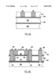
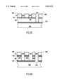
- FIG. 1 is cross-sectional view of a preferred embodiment multi-layered semiconductor structure
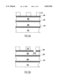
- FIGS. 2A-B show a preferred embodiment diode formed in the layered structure of FIG. 1;
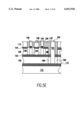
- FIGS. 3A-B show a preferred embodiment bipolar transistor formed in the layered structure of FIG. 1;
- FIGS. 4A-B show a preferred embodiment FET formed in the layered structure 100 of FIG. 1;
- FIGS. 5A-E show a first alternate embodiment method of forming the preferred embodiment FET, which includes at least one additional buried oxide layer and at least one additional silicon layer;
- FIGS. 6A-E show a second alternate embodiment method of forming the preferred embodiment FET.
- the preferred embodiment structure is formed in a semiconductor wafer 100, preferably silicon, by implanting oxygen, which during a subsequent anneal reacts with the silicon to form buried oxide (SiO 2 ) layers 102, 104.
- a semiconductor wafer 100 preferably silicon
- oxygen which during a subsequent anneal reacts with the silicon to form buried oxide (SiO 2 ) layers 102, 104.
- SiO 2 buried oxide
- individual silicon layers 106, 108 and 110 are formed and isolated from each other by oxide layers 102, 104.
- any number of buried layers 102, 104 may be formed using multiple oxygen implants to form a multi-layered structure, i.e., implanting n oxygen layers to define n+1 silicon layers, where n is a positive integer.
- the multi-layer structure 100 of FIG. 1 may be formed by any appropriate manner. So, for example, a single insulator (SiO 2 ) layer may be formed on a surface of two or more silicon wafers. Then, these oxidized wafers may be bonded together, sandwiching a layer of oxide 102 between two thick silicon layers 106, 108. One silicon layer 108 is ground to a desired thickness and the ground surface (not shown) is oxidized. A third oxidized wafer is bonded to the newly formed oxide, forming a second oxide layer 104. The silicon layer 110 on third oxide layer 104 is ground to a desired thickness to form multi-layer wafer 100 of FIG. 1.
- SiO 2 silicon oxide layer
- a preferred embodiment diode may be formed on the wafer 100 as shown in FIGS. 2A-B.
- a shallow trench 120 is opened in surface silicon layer 110 down to buried oxide layer 104.
- buried oxide layer 104 acts as an etch stop during trench 120 etch.
- the trench 120 is filled with oxide and the oxide is planarized.
- Deep trenches 122 and 124 are formed at either end of shallow trench 120. Deep trenches 122 and 124 extend down through buried oxide layer 104 and buried silicon layer 108 to second buried oxide layer 102, isolating section 126. Preferably, buried layer 108 is lightly doped either P-type or N-type. A multi-step etch is used to etch deep trenches 122 and 124, each buried oxide layer 104 and 102 acting as an etch stop to etching silicon layers 110 and 108, respectively.
- a diode junction is formed in the section 126 between deep trenches 122 and 124, which are filled with conducting material.
- one deep trench 122 is filled with heavily doped polysilicon, doped with the same dopant type as isolated section 126, e.g. P-type.
- the other trench 124 is filled with heavily doped polysilicon, doped with the other dopant type, N-type in this example. The wafer is heated sufficiently that dopant from the doped polysilicon in the deep trenches out-diffuses into isolated section 126, forming the diode junction there.
- sidewalls 128 of section 126 are exposed and are selectively doped with opposite dopant types.
- the dopants are diffused into the section 126 to form the diode.
- the deep trenches 122, 124 are filled with metal.
- the sidewall 128 doping may be to a level sufficient to form an ohmic contact.
- a resistor may be formed, instead of a diode, by filling both deep trenches 122, 124 with heavily doped polysilicon, doped with the same dopant type as section 126.
- both sidewalls 128 may be heavily doped with the same dopant type as section 126 and, the trenches 122, 124 filled with metal.
- additional deep trenches may be formed outboard of the preferred embodiment device and filled with insulator to completely isolate the preferred embodiment device from other devices on the same chip or, even, from other devices in the same circuit.
- a preferred embodiment bipolar transistor is formed in the layered wafer 100 in FIGS. 3A-B.
- a pair of shallow trenches 130 are opened in surface silicon layer 110 down to buried oxide layer 104.
- buried oxide layer 104 acts as an etch stop during shallow trench 130 etch.
- the shallow trenches 130 are filled with oxide and the oxide is planarized.
- Deep trenches 132 are formed outboard of shallow trenches 130. Deep trenches 132 are emitter and collector openings for the preferred embodiment lateral bipolar transistor. As with the preferred embodiment diode of FIGS. 2A-B, deep trenches 132 extend down through buried oxide layer 104 and buried silicon layer 108 to second buried oxide layer 102, isolating section 134. As with the preferred embodiment diode, buried layer 108 is, preferably, lightly doped either p-type or n-type, depending on the intended bipolar transistor type, i.e., whether pnp or npn. A multi-step etch is used to etch deep trenches 132, each buried oxide layer 104 and 102 acting as an etch stop to etching silicon layers 110 and 108, respectively.
- Emitter and collector regions 136 may be formed identically to forming the diode junction of the above preferred embodiment, except that both are formed of the same type dopant and simultaneously. Thus, if section 134 is P-type, then both emitter and collector regions 136 are N-type and vice versa. Also, the emitter and collector regions 136 may be formed by filling the deep trenches 132 with heavily doped polysilicon, which outdiffuses to form diffusion regions 136; or, regions 136 may be formed by sidewall doping with the deep trenches filled with metal.
- a shallow trench 138 is opened between trenches 132 though surface silicon layer 110 down through buried oxide layer 104 to base section 134.
- a base contact 140 is formed in base section 134 and the shallow trench 138 is filled with conducting material.
- the ohmic base contact region 140 may be formed by filling the shallow trench 138 with heavily doped polysilicon, doped with the same dopant type as section 134 or, alternately, by implanting the same dopant type into base region 140 and, then, filling the shallow trench 138 with metal.
- additional deep trenches may be included to further isolate the preferred embodiment bipolar transistor from surrounding structures and devices.
- a preferred embodiment FET is formed in the layered structure 100 of FIG. 1.
- a pair of shallow trenches 150 are opened in surface silicon layer 110 down to buried oxide layer 104. Again, it is preferred that buried oxide layer 104 acts as an etch stop during shallow trench 150 etch.
- the shallow trenches 150 are filled with oxide and the oxide is planarized.
- Deep trenches 152 are source and drain openings for the preferred embodiment FETs. Deep trenches 152 extend down through buried oxide layer 104 and buried silicon layer 108 to second buried oxide layer 102, isolating channel section 154. Depending on the type of FETs desired, buried layer 108 is, preferably, lightly doped either p-type or n-type. A multi-step etch is used to etch deep trenches 152, each buried oxide layer 104 and 102 acting as an etch stop to etching silicon layers 110 and 108, respectively.
- Lower gate contact deep trenches 156 are formed simultaneously with deep trenches 152.
- Lower gate contact trenches 156 are etched through second buried layer 102 to lower silicon layer 106.
- lower gate contact trenches 156 may be etched into lower silicon layer 106 or, through lower silicon layer 106.
- Source/drain diffusions 158 are formed at opposite ends of channel section 154.
- Source/drain diffusions 158 may be formed identically to forming emitter and collector regions 136 of the above preferred bipolar transistor embodiment. Thus, if channel section 154 is p-type, then both source and drain diffusions 158 are n-type and vice versa.
- the source and drain diffusions 158 may be formed by filling the deep trenches 152 with heavily doped polysilicon, which outdiffuses forming diffusions 158; or, they may be formed by sidewall doping and diffusing the dopant into the ends of the channel section 154 in the deep trenches 152, which are then filled with metal.
- a lower gate contact 156' is formed to lower silicon layer 106 through deep trenches 156.
- Lower gate layer 106 is doped to a much higher dopant concentration than channel section 154 such that the gate is a conductor.
- the lower gate layer 106 may be doped with any dopant type, provided it is doped to be sufficiently conductive.
- This lower gate contact 156' may be formed by filling the deep trenches 156 with heavily doped polysilicon, which forms an ohmic contact to lower silicon layer 106; or, alternately, by heavily doping exposed surfaces of lower silicon layer 106 and then, filling the deep trenches 154 with metal.
- upper gate contacts 160 are formed to upper gate segments 162.
- a portion of upper gate segment 162 may be heavily doped to form an ohmic contact.
- metal wiring or contact studs are formed on the four device terminals: source/drain contacts 164, lower gate contact 166 and upper gate contact 160.
- the preferred embodiment FET has a gate both above 162 and below 106 its channel. This pair of gates for preferred embodiment FETs eliminates the vertical structural asymmetry of prior art devices.
- FIGS. 5A-E show a first alternate embodiment method of forming the preferred embodiment FET, which includes at least one additional buried oxide layer 170 and, as a result, at least one additional silicon layer 172.
- the surface layer 110 is selectively removed to define the upper gate 174.
- the upper oxide layer 104 acts as an etch stop.
- the lower gate contact trench 176 is partially etched, selectively, through upper oxide layer 104 and channel layer 108 to lower oxide layer 102.
- FIG. 5C the opened trenches are filled with oxide 178 and the surface 180 is planarized.
- the oxide fill 178 is patterned and directionally etched, selective to silicon, until trenches 182 are opened.
- Trenches 182 extend through the fill oxide 178 to channel layer 108 in source/drain regions.
- a lower gate contact trench 184 to lower gate layer 106 is opened coincident with opening trenches 182.
- An oxide spacer 178' remains between the lower gate contact trench 184 and source/drain trenches 182, while oxide lines each trench 182, 184. Having exposed silicon layer 108 in source/drain regions through trenches 182 and lower gate layer 106 in lower gate contact trench 184, the exposed portions of the silicon layers 106, 108 are etched, directionally, down to the next lowest buried oxide layer 102, 172, respectively.
- source/drain diffusions 186 and lower gate contact 188 are formed and, the trenches 182, 184 are filled with conducting material 190, 192, respectively.
- the source/drain diffusions 186 and lower gate contact 188 may be formed by filling the opened trenches 182, 184 with heavily doped polysilicon 190, 192, which forms diffusions 186 and an ohmic contact 188 through outdoping.
- exposed sidewalls of silicon layers 106, 108 are doped sufficiently such that source/drain diffusions 186 form during a subsequent anneal step.
- An ohmic contact 188 is formed and remains ohmic after the anneal step. This diffusion/contact formation is followed by filling the opened trenches 182, 184 with metal 190, 192.
- a top gate contact 194 may be formed coincidentally with ohmic contact 188, and is also intended to be an ohmic contact. Having filled the open trenches with conductive material 190, 192, such as heavily doped polysilicon or metal, conductive caps or, studs 196, preferably of metal are formed for subsequent connection.
- FIGS. 6A-E show a second alternate embodiment method of forming the preferred embodiment FET.
- shallow trenches 200, 202 and 204 are etched through top silicon layer 110 to upper buried oxide layer 104.
- silicon etching continues until second buried oxide layer 102 is reached, forming deep trench 204 ⁇ in FIG. 6B.
- a conformal oxide layer 206 in FIG. 6C is formed on the structure of FIG. 6B.
- oxide is removed from the bottom of the trenches 200, 202 and 204', exposing silicon layers 108 and 106, respectively.
- the exposed portions of layer 108 are directionally etched until lower buried layer 102 is reached. At this point sidewalls 208 and lower gate contact area 210 have been exposed.
- source/drain diffusions 212 and lower gate contact 214 are formed and, the trenches 200, 202 and 204' are filled with conducting material 216, 218 and 220, respectively.
- the source/drain diffusions 212 and lower gate contact 214 may be formed by filling the opened trenches 200, 202 and 204' with heavily doped polysilicon 216, 218 and 220, which forms diffusions 212 and an ohmic contact 214 through outdiffusion.
- exposed sidewalls of silicon layer 106 are doped sufficiently such that source/drain diffusions 212 form during a subsequent anneal step.
- An ohmic contact 214 forms in lower gate layer 106 and remains ohmic after the anneal step. This is followed by filling the opened trenches 200, 202 and 204' with metal 216, 218 and 220.
- a opening may be formed through to gate 222 and a top gate contact 224 may be formed coincidentally with ohmic contact 214.
- Top gate contact 224 is also intended to be an ohmic contact. Having formed the top gate contact 224 and filled trenches 200, 202 and 204' with conductive material 216, 218 and 220, such as heavily doped polysilicon or metal, conductive caps or studs 226, preferably of metal are formed for subsequent connection.
Abstract
Description
Claims (17)
Priority Applications (5)
| Application Number | Priority Date | Filing Date | Title |
|---|---|---|---|
| US09/130,299 US6013936A (en) | 1998-08-06 | 1998-08-06 | Double silicon-on-insulator device and method therefor |
| US09/225,315 US6383892B1 (en) | 1998-08-06 | 1999-01-05 | Double silicon-on-insulator device and method thereof |
| TW088101935A TW451419B (en) | 1998-08-06 | 1999-02-09 | Double silicon-on-insulator device and method therefor |
| KR1019990029924A KR20000016967A (en) | 1998-08-06 | 1999-07-23 | Double silicon-on- insulator device and method therefor |
| JP21464099A JP3382182B2 (en) | 1998-08-06 | 1999-07-29 | Method of forming FET, diode, bipolar transistor and buried resistor |
Applications Claiming Priority (1)
| Application Number | Priority Date | Filing Date | Title |
|---|---|---|---|
| US09/130,299 US6013936A (en) | 1998-08-06 | 1998-08-06 | Double silicon-on-insulator device and method therefor |
Related Child Applications (1)
| Application Number | Title | Priority Date | Filing Date |
|---|---|---|---|
| US09/225,315 Division US6383892B1 (en) | 1998-08-06 | 1999-01-05 | Double silicon-on-insulator device and method thereof |
Publications (1)
| Publication Number | Publication Date |
|---|---|
| US6013936A true US6013936A (en) | 2000-01-11 |
Family
ID=22444028
Family Applications (2)
| Application Number | Title | Priority Date | Filing Date |
|---|---|---|---|
| US09/130,299 Expired - Lifetime US6013936A (en) | 1998-08-06 | 1998-08-06 | Double silicon-on-insulator device and method therefor |
| US09/225,315 Expired - Fee Related US6383892B1 (en) | 1998-08-06 | 1999-01-05 | Double silicon-on-insulator device and method thereof |
Family Applications After (1)
| Application Number | Title | Priority Date | Filing Date |
|---|---|---|---|
| US09/225,315 Expired - Fee Related US6383892B1 (en) | 1998-08-06 | 1999-01-05 | Double silicon-on-insulator device and method thereof |
Country Status (4)
| Country | Link |
|---|---|
| US (2) | US6013936A (en) |
| JP (1) | JP3382182B2 (en) |
| KR (1) | KR20000016967A (en) |
| TW (1) | TW451419B (en) |
Cited By (39)
| Publication number | Priority date | Publication date | Assignee | Title |
|---|---|---|---|---|
| US6084284A (en) * | 1994-11-18 | 2000-07-04 | Adamic, Jr.; Fred W. | Integrated circuit including inverted dielectric isolation |
| US6287901B1 (en) * | 2000-01-05 | 2001-09-11 | International Business Machines Corporation | Method and semiconductor structure for implementing dual plane body contacts for silicon-on-insulator (SOI) transistors |
| US6436744B1 (en) * | 2001-03-16 | 2002-08-20 | International Business Machines Corporation | Method and structure for creating high density buried contact for use with SOI processes for high performance logic |
| US6468880B1 (en) | 2001-03-15 | 2002-10-22 | Chartered Semiconductor Manufacturing Ltd. | Method for fabricating complementary silicon on insulator devices using wafer bonding |
| US6492244B1 (en) * | 2001-11-21 | 2002-12-10 | International Business Machines Corporation | Method and semiconductor structure for implementing buried dual rail power distribution and integrated decoupling capacitance for silicon on insulator (SOI) devices |
| US20020190331A1 (en) * | 2001-06-15 | 2002-12-19 | Agere Systems Guardian Corp. | A semiconductor device having at least one source/drain region formed on an isolation region and a method of manufacture therefor |
| US6613652B2 (en) | 2001-03-14 | 2003-09-02 | Chartered Semiconductor Manufacturing Ltd. | Method for fabricating SOI devices with option of incorporating air-gap feature for better insulation and performance |
| US6645795B2 (en) * | 2001-05-03 | 2003-11-11 | International Business Machines Corporation | Polysilicon doped transistor using silicon-on-insulator and double silicon-on-insulator |
| US6649964B2 (en) * | 2000-09-22 | 2003-11-18 | Hynix Semiconductor, Inc. | Body-to-substrate contact structure for SOI device and method for fabricating same |
| US20040085477A1 (en) * | 2002-10-30 | 2004-05-06 | The University Of Chicago | Method to smooth photometric variations across multi-projector displays |
| US20040085256A1 (en) * | 2002-10-30 | 2004-05-06 | The University Of Chicago | Methods and measurement engine for aligning multi-projector display systems |
| US20040219760A1 (en) * | 2002-08-29 | 2004-11-04 | Micro Technology, Inc. | Cascode I/O driver with improved ESD operation |
| US20040227181A1 (en) * | 2003-05-15 | 2004-11-18 | Yeo Kyoung-Hwan | Multichannel metal oxide semiconductor (MOS) transistors and methods of fabricating the same |
| US6853048B1 (en) * | 2000-08-11 | 2005-02-08 | Agere Systems Inc. | Bipolar transistor having an isolation structure located under the base, emitter and collector and a method of manufacture thereof |
| US20050035423A1 (en) * | 2003-07-08 | 2005-02-17 | Infineon Technologies Ag | Electronic device with guard ring |
| US6864547B2 (en) | 2001-06-15 | 2005-03-08 | Agere Systems Inc. | Semiconductor device having a ghost source/drain region and a method of manufacture therefor |
| US20060102223A1 (en) * | 2004-11-12 | 2006-05-18 | Chen Howard H | Integrated thermoelectric cooling devices and methods for fabricating same |
| US20070026584A1 (en) * | 2005-07-29 | 2007-02-01 | Texas Instruments Inc. | Dielectric isolated body biasing of silicon on insulator |
| US20080048287A1 (en) * | 2002-09-29 | 2008-02-28 | Advanced Analogic Technologies, Inc. | Isolation structures for integrated circuits and modular methods of forming the same |
| US20080197446A1 (en) * | 2002-08-14 | 2008-08-21 | Advanced Analogic Technologies, Inc. | Isolated diode |
| US20080197408A1 (en) * | 2002-08-14 | 2008-08-21 | Advanced Analogic Technologies, Inc. | Isolated quasi-vertical DMOS transistor |
| US20080213972A1 (en) * | 2002-08-14 | 2008-09-04 | Advanced Analogic Technologies, Inc. | Processes for forming isolation structures for integrated circuit devices |
| US20080210980A1 (en) * | 2002-08-14 | 2008-09-04 | Advanced Analogic Technologies, Inc. | Isolated CMOS transistors |
| US20080217729A1 (en) * | 2002-08-14 | 2008-09-11 | Advanced Analogic Technologies, Inc. | Isolation structures for integrated circuit devices |
| US20080217699A1 (en) * | 2002-08-14 | 2008-09-11 | Advanced Analogic Technologies, Inc. | Isolated Bipolar Transistor |
| US20080230812A1 (en) * | 2002-08-14 | 2008-09-25 | Advanced Analogic Technologies, Inc. | Isolated junction field-effect transistor |
| US20080237783A1 (en) * | 2007-03-28 | 2008-10-02 | Advanced Analogic Technologies, Inc. | Isolated bipolar transistor |
| US20080237704A1 (en) * | 2007-03-28 | 2008-10-02 | Advanced Analogic Technologies, Inc. | Isolated trench MOSFET |
| US20090096501A1 (en) * | 2007-10-10 | 2009-04-16 | Atmel Corporation | Apparatus and method for preventing snap back in integrated circuits |
| US20090152668A1 (en) * | 2007-12-14 | 2009-06-18 | Denso Dorporation | Semiconductor apparatus |
| US20090321875A1 (en) * | 2008-06-30 | 2009-12-31 | Vanguard International Semiconductor Corporation | Semiconductor device and fabrication method thereof |
| US20100133611A1 (en) * | 2002-08-14 | 2010-06-03 | Advanced Analogic Technologies, Inc. | Isolated transistor |
| US20100149710A1 (en) * | 2008-12-12 | 2010-06-17 | Atmel Corporation | Snap-back tolerant integrated circuits |
| US20100176480A1 (en) * | 2009-01-15 | 2010-07-15 | Denso Corporation | Semiconductor device, method for manufacturing the same, and multilayer substrate having the same |
| US20110201171A1 (en) * | 2002-08-14 | 2011-08-18 | Advanced Analogic Technologies, Inc. | Processes For Forming Isolation Structures For Integrated Circuit Devices |
| US8285353B2 (en) | 2006-10-11 | 2012-10-09 | Korea Advanced Institute Of Science And Technology | System for analyzing tissue perfusion using concentration of indocyanine green in blood |
| US20150145039A1 (en) * | 2013-11-26 | 2015-05-28 | Taiwan Semiconductor Manufacturing Company, Ltd. | Semiconductor device having drain side contact through buried oxide |
| WO2018011587A1 (en) * | 2016-07-13 | 2018-01-18 | Rockley Photonics Limited | Mode converter and method of fabricating thereof |
| CN116403902A (en) * | 2023-06-08 | 2023-07-07 | 微龛(广州)半导体有限公司 | Vertical bipolar junction transistor and manufacturing method thereof |
Families Citing this family (7)
| Publication number | Priority date | Publication date | Assignee | Title |
|---|---|---|---|---|
| US7163864B1 (en) * | 2000-10-18 | 2007-01-16 | International Business Machines Corporation | Method of fabricating semiconductor side wall fin |
| JP3664704B2 (en) * | 2002-10-03 | 2005-06-29 | 沖電気工業株式会社 | Semiconductor device |
| DE10361714B4 (en) * | 2003-12-30 | 2009-06-10 | Infineon Technologies Ag | Semiconductor device |
| DE102004004512B4 (en) * | 2004-01-23 | 2008-07-10 | Atmel Germany Gmbh | Integrated circuit with lateral dielectric isolation of active regions via electrically contacted buried material and manufacturing process |
| JP4845357B2 (en) * | 2004-08-26 | 2011-12-28 | ラピスセミコンダクタ株式会社 | Semiconductor device and manufacturing method thereof |
| DE102015105816A1 (en) * | 2015-04-16 | 2016-10-20 | Infineon Technologies Dresden Gmbh | Semiconductor device with electrostatic discharge protection structure |
| DE102015108537B4 (en) | 2015-05-29 | 2019-07-04 | Infineon Technologies Dresden Gmbh | Semiconductor device with electrostatic discharge protection structure |
Citations (23)
| Publication number | Priority date | Publication date | Assignee | Title |
|---|---|---|---|---|
| US3622382A (en) * | 1969-05-05 | 1971-11-23 | Ibm | Semiconductor isolation structure and method of producing |
| US4412868A (en) * | 1981-12-23 | 1983-11-01 | General Electric Company | Method of making integrated circuits utilizing ion implantation and selective epitaxial growth |
| US4596070A (en) * | 1984-07-13 | 1986-06-24 | Texas Instruments Incorporated | Interdigitated IMPATT devices |
| US4601760A (en) * | 1984-05-09 | 1986-07-22 | Analog Devices, Incorporated | Ion-implanted process for forming IC wafer with buried-reference diode and IC structure made with such process |
| US4997786A (en) * | 1986-06-13 | 1991-03-05 | Matsushita Electric Industrial Co., Ltd. | Method of fabricating a semiconductor device having buried insulation layer separated by ditches |
| US5083190A (en) * | 1989-09-05 | 1992-01-21 | Motorola, Inc. | Shared gate CMOS transistor |
| US5138437A (en) * | 1987-07-27 | 1992-08-11 | Mitsubishi Denki Kabushiki Kaisha | Semiconductor integrated circuit device in which integrated circuit units having different functions are stacked in three dimensional manner |
| US5164805A (en) * | 1988-08-22 | 1992-11-17 | Massachusetts Institute Of Technology | Near-intrinsic thin-film SOI FETS |
| US5273921A (en) * | 1991-12-27 | 1993-12-28 | Purdue Research Foundation | Methods for fabricating a dual-gated semiconductor-on-insulator field effect transistor |
| US5382818A (en) * | 1993-12-08 | 1995-01-17 | Philips Electronics North America Corporation | Lateral semiconductor-on-insulator (SOI) semiconductor device having a buried diode |
| US5420048A (en) * | 1991-01-09 | 1995-05-30 | Canon Kabushiki Kaisha | Manufacturing method for SOI-type thin film transistor |
| US5422305A (en) * | 1993-10-29 | 1995-06-06 | Texas Instruments Incorporated | Method of forming implanted silicon resonant tunneling barriers |
| US5442223A (en) * | 1990-10-17 | 1995-08-15 | Nippondenso Co., Ltd. | Semiconductor device with stress relief |
| US5461250A (en) * | 1992-08-10 | 1995-10-24 | International Business Machines Corporation | SiGe thin film or SOI MOSFET and method for making the same |
| US5494846A (en) * | 1993-12-17 | 1996-02-27 | Nec Corporation | Method of manufacturing semiconductor device |
| JPH08148567A (en) * | 1994-11-24 | 1996-06-07 | Sanyo Electric Co Ltd | Manufacture of semiconductor device |
| JPH08148556A (en) * | 1994-11-16 | 1996-06-07 | Sony Corp | Semiconductor device and its manufacture |
| US5536966A (en) * | 1992-09-22 | 1996-07-16 | National Semiconductor Corporation | Retrograde NWell cathode Schottky transistor and fabrication process |
| US5548149A (en) * | 1993-06-24 | 1996-08-20 | Texas Instruments Incorporated | Varying the thickness of the surface silicon layer in a silicon-on-insulator substrate |
| JPH0945765A (en) * | 1995-07-26 | 1997-02-14 | Sony Corp | Manufacture of semiconductor device with multilayer interconnection structure |
| JPH09129885A (en) * | 1995-10-26 | 1997-05-16 | Matsushita Electric Works Ltd | Semiconductor device |
| JPH09232424A (en) * | 1996-02-21 | 1997-09-05 | Nec Kyushu Ltd | Manufacture of semiconductor device |
| US5689127A (en) * | 1996-03-05 | 1997-11-18 | International Business Machines Corporation | Vertical double-gate field effect transistor |
Family Cites Families (2)
| Publication number | Priority date | Publication date | Assignee | Title |
|---|---|---|---|---|
| DE69332407T2 (en) * | 1992-06-17 | 2003-06-18 | Harris Corp | Manufacture of semiconductor devices on SOI substrates |
| US5808330A (en) * | 1994-11-02 | 1998-09-15 | Lsi Logic Corporation | Polydirectional non-orthoginal three layer interconnect architecture |
-
1998
- 1998-08-06 US US09/130,299 patent/US6013936A/en not_active Expired - Lifetime
-
1999
- 1999-01-05 US US09/225,315 patent/US6383892B1/en not_active Expired - Fee Related
- 1999-02-09 TW TW088101935A patent/TW451419B/en not_active IP Right Cessation
- 1999-07-23 KR KR1019990029924A patent/KR20000016967A/en active Search and Examination
- 1999-07-29 JP JP21464099A patent/JP3382182B2/en not_active Expired - Fee Related
Patent Citations (24)
| Publication number | Priority date | Publication date | Assignee | Title |
|---|---|---|---|---|
| US3622382A (en) * | 1969-05-05 | 1971-11-23 | Ibm | Semiconductor isolation structure and method of producing |
| US4412868A (en) * | 1981-12-23 | 1983-11-01 | General Electric Company | Method of making integrated circuits utilizing ion implantation and selective epitaxial growth |
| US4601760A (en) * | 1984-05-09 | 1986-07-22 | Analog Devices, Incorporated | Ion-implanted process for forming IC wafer with buried-reference diode and IC structure made with such process |
| US4596070A (en) * | 1984-07-13 | 1986-06-24 | Texas Instruments Incorporated | Interdigitated IMPATT devices |
| US4997786A (en) * | 1986-06-13 | 1991-03-05 | Matsushita Electric Industrial Co., Ltd. | Method of fabricating a semiconductor device having buried insulation layer separated by ditches |
| US5138437A (en) * | 1987-07-27 | 1992-08-11 | Mitsubishi Denki Kabushiki Kaisha | Semiconductor integrated circuit device in which integrated circuit units having different functions are stacked in three dimensional manner |
| US5164805A (en) * | 1988-08-22 | 1992-11-17 | Massachusetts Institute Of Technology | Near-intrinsic thin-film SOI FETS |
| US5083190A (en) * | 1989-09-05 | 1992-01-21 | Motorola, Inc. | Shared gate CMOS transistor |
| US5442223A (en) * | 1990-10-17 | 1995-08-15 | Nippondenso Co., Ltd. | Semiconductor device with stress relief |
| US5420048A (en) * | 1991-01-09 | 1995-05-30 | Canon Kabushiki Kaisha | Manufacturing method for SOI-type thin film transistor |
| US5273921A (en) * | 1991-12-27 | 1993-12-28 | Purdue Research Foundation | Methods for fabricating a dual-gated semiconductor-on-insulator field effect transistor |
| US5349228A (en) * | 1991-12-27 | 1994-09-20 | Purdue Research Foundation | Dual-gated semiconductor-on-insulator field effect transistor |
| US5461250A (en) * | 1992-08-10 | 1995-10-24 | International Business Machines Corporation | SiGe thin film or SOI MOSFET and method for making the same |
| US5536966A (en) * | 1992-09-22 | 1996-07-16 | National Semiconductor Corporation | Retrograde NWell cathode Schottky transistor and fabrication process |
| US5548149A (en) * | 1993-06-24 | 1996-08-20 | Texas Instruments Incorporated | Varying the thickness of the surface silicon layer in a silicon-on-insulator substrate |
| US5422305A (en) * | 1993-10-29 | 1995-06-06 | Texas Instruments Incorporated | Method of forming implanted silicon resonant tunneling barriers |
| US5382818A (en) * | 1993-12-08 | 1995-01-17 | Philips Electronics North America Corporation | Lateral semiconductor-on-insulator (SOI) semiconductor device having a buried diode |
| US5494846A (en) * | 1993-12-17 | 1996-02-27 | Nec Corporation | Method of manufacturing semiconductor device |
| JPH08148556A (en) * | 1994-11-16 | 1996-06-07 | Sony Corp | Semiconductor device and its manufacture |
| JPH08148567A (en) * | 1994-11-24 | 1996-06-07 | Sanyo Electric Co Ltd | Manufacture of semiconductor device |
| JPH0945765A (en) * | 1995-07-26 | 1997-02-14 | Sony Corp | Manufacture of semiconductor device with multilayer interconnection structure |
| JPH09129885A (en) * | 1995-10-26 | 1997-05-16 | Matsushita Electric Works Ltd | Semiconductor device |
| JPH09232424A (en) * | 1996-02-21 | 1997-09-05 | Nec Kyushu Ltd | Manufacture of semiconductor device |
| US5689127A (en) * | 1996-03-05 | 1997-11-18 | International Business Machines Corporation | Vertical double-gate field effect transistor |
Non-Patent Citations (2)
| Title |
|---|
| R. F. Brom et al., "Vertical Schottky Diode-Memory Device", IBM Technical Bulletin, vol. 15. No. 7, Dec. 1972. |
| R. F. Brom et al., Vertical Schottky Diode Memory Device , IBM Technical Bulletin, vol. 15. No. 7, Dec. 1972. * |
Cited By (98)
| Publication number | Priority date | Publication date | Assignee | Title |
|---|---|---|---|---|
| US6084284A (en) * | 1994-11-18 | 2000-07-04 | Adamic, Jr.; Fred W. | Integrated circuit including inverted dielectric isolation |
| US6528853B2 (en) | 2000-01-05 | 2003-03-04 | International Business Machines Corporation | Method and semiconductor structure for implementing dual plane body contacts for silicon-on-insulator (SOI) transistors |
| US6287901B1 (en) * | 2000-01-05 | 2001-09-11 | International Business Machines Corporation | Method and semiconductor structure for implementing dual plane body contacts for silicon-on-insulator (SOI) transistors |
| US6853048B1 (en) * | 2000-08-11 | 2005-02-08 | Agere Systems Inc. | Bipolar transistor having an isolation structure located under the base, emitter and collector and a method of manufacture thereof |
| US6649964B2 (en) * | 2000-09-22 | 2003-11-18 | Hynix Semiconductor, Inc. | Body-to-substrate contact structure for SOI device and method for fabricating same |
| US6613652B2 (en) | 2001-03-14 | 2003-09-02 | Chartered Semiconductor Manufacturing Ltd. | Method for fabricating SOI devices with option of incorporating air-gap feature for better insulation and performance |
| US6468880B1 (en) | 2001-03-15 | 2002-10-22 | Chartered Semiconductor Manufacturing Ltd. | Method for fabricating complementary silicon on insulator devices using wafer bonding |
| US6436744B1 (en) * | 2001-03-16 | 2002-08-20 | International Business Machines Corporation | Method and structure for creating high density buried contact for use with SOI processes for high performance logic |
| US6645795B2 (en) * | 2001-05-03 | 2003-11-11 | International Business Machines Corporation | Polysilicon doped transistor using silicon-on-insulator and double silicon-on-insulator |
| US20020190331A1 (en) * | 2001-06-15 | 2002-12-19 | Agere Systems Guardian Corp. | A semiconductor device having at least one source/drain region formed on an isolation region and a method of manufacture therefor |
| US6958518B2 (en) | 2001-06-15 | 2005-10-25 | Agere Systems Inc. | Semiconductor device having at least one source/drain region formed on an isolation region and a method of manufacture therefor |
| US6864547B2 (en) | 2001-06-15 | 2005-03-08 | Agere Systems Inc. | Semiconductor device having a ghost source/drain region and a method of manufacture therefor |
| US20030094654A1 (en) * | 2001-11-21 | 2003-05-22 | International Business Machines Corporation | Method and semiconductor structure for implementing buried dual rail power distribution and integrated decoupling capacitance for silicon on insulator (SOI) devices |
| US6492244B1 (en) * | 2001-11-21 | 2002-12-10 | International Business Machines Corporation | Method and semiconductor structure for implementing buried dual rail power distribution and integrated decoupling capacitance for silicon on insulator (SOI) devices |
| US6667518B2 (en) * | 2001-11-21 | 2003-12-23 | International Business Machines Corporation | Method and semiconductor structure for implementing buried dual rail power distribution and integrated decoupling capacitance for silicon on insulator (SOI) devices |
| US8097522B2 (en) | 2002-08-14 | 2012-01-17 | Advanced Analogic Technologies, Inc. | Modular methods of forming isolation structures for integrated circuits |
| US8664715B2 (en) | 2002-08-14 | 2014-03-04 | Advanced Analogic Technologies Incorporated | Isolated transistor |
| US7834421B2 (en) | 2002-08-14 | 2010-11-16 | Advanced Analogic Technologies, Inc. | Isolated diode |
| US7902630B2 (en) | 2002-08-14 | 2011-03-08 | Advanced Analogic Technologies, Inc. | Isolated bipolar transistor |
| US20100133611A1 (en) * | 2002-08-14 | 2010-06-03 | Advanced Analogic Technologies, Inc. | Isolated transistor |
| US7939420B2 (en) | 2002-08-14 | 2011-05-10 | Advanced Analogic Technologies, Inc. | Processes for forming isolation structures for integrated circuit devices |
| US7956391B2 (en) * | 2002-08-14 | 2011-06-07 | Advanced Analogic Technologies, Inc. | Isolated junction field-effect transistor |
| US20110201171A1 (en) * | 2002-08-14 | 2011-08-18 | Advanced Analogic Technologies, Inc. | Processes For Forming Isolation Structures For Integrated Circuit Devices |
| US20090236683A1 (en) * | 2002-08-14 | 2009-09-24 | Advanced Analogic Technologies, Inc. | Isolation structures for integrated circuits |
| US8089129B2 (en) | 2002-08-14 | 2012-01-03 | Advanced Analogic Technologies, Inc. | Isolated CMOS transistors |
| US7812403B2 (en) | 2002-08-14 | 2010-10-12 | Advanced Analogic Technologies, Inc. | Isolation structures for integrated circuit devices |
| US8513087B2 (en) | 2002-08-14 | 2013-08-20 | Advanced Analogic Technologies, Incorporated | Processes for forming isolation structures for integrated circuit devices |
| US8659116B2 (en) | 2002-08-14 | 2014-02-25 | Advanced Analogic Technologies Incorporated | Isolated transistor |
| US20080197446A1 (en) * | 2002-08-14 | 2008-08-21 | Advanced Analogic Technologies, Inc. | Isolated diode |
| US20080197408A1 (en) * | 2002-08-14 | 2008-08-21 | Advanced Analogic Technologies, Inc. | Isolated quasi-vertical DMOS transistor |
| US20080213972A1 (en) * | 2002-08-14 | 2008-09-04 | Advanced Analogic Technologies, Inc. | Processes for forming isolation structures for integrated circuit devices |
| US20080210980A1 (en) * | 2002-08-14 | 2008-09-04 | Advanced Analogic Technologies, Inc. | Isolated CMOS transistors |
| US20080217729A1 (en) * | 2002-08-14 | 2008-09-11 | Advanced Analogic Technologies, Inc. | Isolation structures for integrated circuit devices |
| US20080217699A1 (en) * | 2002-08-14 | 2008-09-11 | Advanced Analogic Technologies, Inc. | Isolated Bipolar Transistor |
| US20080230812A1 (en) * | 2002-08-14 | 2008-09-25 | Advanced Analogic Technologies, Inc. | Isolated junction field-effect transistor |
| US20080019064A1 (en) * | 2002-08-29 | 2008-01-24 | Micron Technology, Inc. | Cascode i/o driver with improved esd operation |
| US7903379B2 (en) | 2002-08-29 | 2011-03-08 | Micron Technology, Inc. | Cascode I/O driver with improved ESD operation |
| US20040219760A1 (en) * | 2002-08-29 | 2004-11-04 | Micro Technology, Inc. | Cascode I/O driver with improved ESD operation |
| US7253064B2 (en) | 2002-08-29 | 2007-08-07 | Micron Technology, Inc. | Cascode I/O driver with improved ESD operation |
| US9905640B2 (en) | 2002-09-29 | 2018-02-27 | Skyworks Solutions (Hong Kong) Limited | Isolation structures for semiconductor devices including trenches containing conductive material |
| US9257504B2 (en) | 2002-09-29 | 2016-02-09 | Advanced Analogic Technologies Incorporated | Isolation structures for semiconductor devices |
| US8728904B2 (en) | 2002-09-29 | 2014-05-20 | Advanced Analogic Technologies (Hong Kong) Limited | Method of forming isolation structure in semiconductor substrate |
| US10074716B2 (en) | 2002-09-29 | 2018-09-11 | Skyworks Solutions (Hong Kong) Limited | Saucer-shaped isolation structures for semiconductor devices |
| US20080048287A1 (en) * | 2002-09-29 | 2008-02-28 | Advanced Analogic Technologies, Inc. | Isolation structures for integrated circuits and modular methods of forming the same |
| US20040085256A1 (en) * | 2002-10-30 | 2004-05-06 | The University Of Chicago | Methods and measurement engine for aligning multi-projector display systems |
| US20040085477A1 (en) * | 2002-10-30 | 2004-05-06 | The University Of Chicago | Method to smooth photometric variations across multi-projector displays |
| US20100109087A1 (en) * | 2003-05-15 | 2010-05-06 | Yeo Kyoung-Hwan | Multichannel Metal Oxide Semiconductor (MOS) Transistors |
| US7670912B2 (en) | 2003-05-15 | 2010-03-02 | Samsung Electronics Co., Ltd. | Methods of fabricating multichannel metal oxide semiconductor (MOS) transistors |
| US20040227181A1 (en) * | 2003-05-15 | 2004-11-18 | Yeo Kyoung-Hwan | Multichannel metal oxide semiconductor (MOS) transistors and methods of fabricating the same |
| US7307329B2 (en) * | 2003-07-08 | 2007-12-11 | Infineon Technologies Ag | Electronic device with guard ring |
| US20050035423A1 (en) * | 2003-07-08 | 2005-02-17 | Infineon Technologies Ag | Electronic device with guard ring |
| US20060102223A1 (en) * | 2004-11-12 | 2006-05-18 | Chen Howard H | Integrated thermoelectric cooling devices and methods for fabricating same |
| US7544883B2 (en) * | 2004-11-12 | 2009-06-09 | International Business Machines Corporation | Integrated thermoelectric cooling devices and methods for fabricating same |
| WO2007016446A2 (en) * | 2005-07-29 | 2007-02-08 | Texas Instruments Incorporated | Dielectric isolated body biasing of silicon on insulator |
| US20070026584A1 (en) * | 2005-07-29 | 2007-02-01 | Texas Instruments Inc. | Dielectric isolated body biasing of silicon on insulator |
| WO2007016446A3 (en) * | 2005-07-29 | 2007-07-12 | Texas Instruments Inc | Dielectric isolated body biasing of silicon on insulator |
| US8071462B2 (en) | 2006-05-31 | 2011-12-06 | Advanced Analogic Technologies, Inc. | Isolation structures for integrated circuits and modular methods of forming the same |
| US7701033B2 (en) | 2006-05-31 | 2010-04-20 | Advanced Analogic Technologies, Inc. | Isolation structures for integrated circuits |
| US20080290449A1 (en) * | 2006-05-31 | 2008-11-27 | Advanced Analogic Technologies, Inc. | Isolation structures for integrated circuits |
| US7825488B2 (en) | 2006-05-31 | 2010-11-02 | Advanced Analogic Technologies, Inc. | Isolation structures for integrated circuits and modular methods of forming the same |
| US20080290451A1 (en) * | 2006-05-31 | 2008-11-27 | Advanced Analogic Technologies, Inc. | Isolation structures for integrated circuits |
| US7800198B2 (en) | 2006-05-31 | 2010-09-21 | Advanced Analogic Technologies, Inc. | Isolation structures for integrated circuits |
| US20080290450A1 (en) * | 2006-05-31 | 2008-11-27 | Advanced Analogic Technologies, Inc. | Isolation structures for integrated circuits |
| US7898060B2 (en) | 2006-05-31 | 2011-03-01 | Advanced Analogic Technologies, Inc. | Isolation structures for integrated circuits |
| US8285353B2 (en) | 2006-10-11 | 2012-10-09 | Korea Advanced Institute Of Science And Technology | System for analyzing tissue perfusion using concentration of indocyanine green in blood |
| US8258575B2 (en) | 2007-03-28 | 2012-09-04 | Advanced Analogic Technologies, Inc. | Isolated drain-centric lateral MOSFET |
| US20080237782A1 (en) * | 2007-03-28 | 2008-10-02 | Advanced Analogic Technologies, Inc. | Isolated rectifier diode |
| US20080237783A1 (en) * | 2007-03-28 | 2008-10-02 | Advanced Analogic Technologies, Inc. | Isolated bipolar transistor |
| US20080237706A1 (en) * | 2007-03-28 | 2008-10-02 | Advanced Analogic Technologies, Inc. | Lateral MOSFET |
| US20080237704A1 (en) * | 2007-03-28 | 2008-10-02 | Advanced Analogic Technologies, Inc. | Isolated trench MOSFET |
| US8030731B2 (en) | 2007-03-28 | 2011-10-04 | Advanced Analogic Technologies, Inc. | Isolated rectifier diode |
| US7737526B2 (en) | 2007-03-28 | 2010-06-15 | Advanced Analogic Technologies, Inc. | Isolated trench MOSFET in epi-less semiconductor sustrate |
| US20080237656A1 (en) * | 2007-03-28 | 2008-10-02 | Advanced Analogic Technologies, Inc. | Isolated junction field-effect transistor |
| US7795681B2 (en) | 2007-03-28 | 2010-09-14 | Advanced Analogic Technologies, Inc. | Isolated lateral MOSFET in epi-less substrate |
| US20110012196A1 (en) * | 2007-03-28 | 2011-01-20 | Advanced Analogic Technologies, Inc. | Isolated drain-centric lateral MOSFET |
| US8138570B2 (en) | 2007-03-28 | 2012-03-20 | Advanced Analogic Technologies, Inc. | Isolated junction field-effect transistor |
| US7868414B2 (en) | 2007-03-28 | 2011-01-11 | Advanced Analogic Technologies, Inc. | Isolated bipolar transistor |
| US7692483B2 (en) | 2007-10-10 | 2010-04-06 | Atmel Corporation | Apparatus and method for preventing snap back in integrated circuits |
| US20090096501A1 (en) * | 2007-10-10 | 2009-04-16 | Atmel Corporation | Apparatus and method for preventing snap back in integrated circuits |
| US20090152668A1 (en) * | 2007-12-14 | 2009-06-18 | Denso Dorporation | Semiconductor apparatus |
| US7829971B2 (en) | 2007-12-14 | 2010-11-09 | Denso Corporation | Semiconductor apparatus |
| US20090321875A1 (en) * | 2008-06-30 | 2009-12-31 | Vanguard International Semiconductor Corporation | Semiconductor device and fabrication method thereof |
| US8907382B2 (en) * | 2008-06-30 | 2014-12-09 | Vanguard International Semiconductor Corporation | Semiconductor device and fabrication method thereof |
| TWI498997B (en) * | 2008-06-30 | 2015-09-01 | Vanguard Int Semiconduct Corp | Semiconductor device and fabrication method thereof |
| US20100149710A1 (en) * | 2008-12-12 | 2010-06-17 | Atmel Corporation | Snap-back tolerant integrated circuits |
| US8085604B2 (en) | 2008-12-12 | 2011-12-27 | Atmel Corporation | Snap-back tolerant integrated circuits |
| US8148809B2 (en) | 2009-01-15 | 2012-04-03 | Denso Corporation | Semiconductor device, method for manufacturing the same, and multilayer substrate having the same |
| US20100176480A1 (en) * | 2009-01-15 | 2010-07-15 | Denso Corporation | Semiconductor device, method for manufacturing the same, and multilayer substrate having the same |
| US20150145039A1 (en) * | 2013-11-26 | 2015-05-28 | Taiwan Semiconductor Manufacturing Company, Ltd. | Semiconductor device having drain side contact through buried oxide |
| CN104681611A (en) * | 2013-11-26 | 2015-06-03 | 台湾积体电路制造股份有限公司 | Semiconductor device having drain side contact through buried oxide layer |
| US9431531B2 (en) * | 2013-11-26 | 2016-08-30 | Taiwan Semiconductor Manufacturing Company, Ltd. | Semiconductor device having drain side contact through buried oxide |
| CN104681611B (en) * | 2013-11-26 | 2017-10-13 | 台湾积体电路制造股份有限公司 | Semiconductor devices with the drain side contact through oxygen buried layer |
| WO2018011587A1 (en) * | 2016-07-13 | 2018-01-18 | Rockley Photonics Limited | Mode converter and method of fabricating thereof |
| CN109642985A (en) * | 2016-07-13 | 2019-04-16 | 洛克利光子有限公司 | Mode converter and its manufacturing method |
| US10643903B2 (en) * | 2016-07-13 | 2020-05-05 | Rockley Photonics Limited | Mode converter and method of fabricating thereof |
| US11133225B2 (en) | 2016-07-13 | 2021-09-28 | Rockley Photonics Limited | Mode converter and method of fabricating thereof |
| CN116403902A (en) * | 2023-06-08 | 2023-07-07 | 微龛(广州)半导体有限公司 | Vertical bipolar junction transistor and manufacturing method thereof |
| CN116403902B (en) * | 2023-06-08 | 2023-08-18 | 微龛(广州)半导体有限公司 | Vertical bipolar junction transistor and manufacturing method thereof |
Also Published As
| Publication number | Publication date |
|---|---|
| US6383892B1 (en) | 2002-05-07 |
| TW451419B (en) | 2001-08-21 |
| JP3382182B2 (en) | 2003-03-04 |
| JP2000082680A (en) | 2000-03-21 |
| KR20000016967A (en) | 2000-03-25 |
Similar Documents
| Publication | Publication Date | Title |
|---|---|---|
| US6013936A (en) | Double silicon-on-insulator device and method therefor | |
| US5872037A (en) | Method for manufacturing a vertical mosfet including a back gate electrode | |
| KR920001403B1 (en) | Method of manufacturing semiconductor integrated circuit device | |
| US4980744A (en) | Semiconductor integrated circuit device and a method for manufacturing the same | |
| US4835115A (en) | Method for forming oxide-capped trench isolation | |
| US6855581B2 (en) | Method for fabricating a high-voltage high-power integrated circuit device | |
| US6191457B1 (en) | Integrated circuit structure having a bipolar transistor with a thick base oxide and a field effect transistor with a thin gate oxide | |
| US7375000B2 (en) | Discrete on-chip SOI resistors | |
| US6313508B1 (en) | Semiconductor device of high-voltage CMOS structure and method of fabricating same | |
| US5060035A (en) | Silicon-on-insulator metal oxide semiconductor device having conductive sidewall structure | |
| US5394007A (en) | Isolated well and method of making | |
| US6693325B1 (en) | Semiconductor device having silicon on insulator and fabricating method therefor | |
| US5191401A (en) | MOS transistor with high breakdown voltage | |
| US5476809A (en) | Semiconductor device and method of manufacturing the same | |
| US6071763A (en) | Method of fabricating layered integrated circuit | |
| US6914308B2 (en) | Vertical PNP bipolar transistor | |
| KR100263790B1 (en) | Semiconductor device and manufacturing method thereof | |
| US6984868B2 (en) | Semiconductor device having a structure for isolating elements | |
| US5960272A (en) | Element-isolating construct of a semiconductor integrated circuit having an offset region between impurity doped regions, and process of manufacturing the construct | |
| US11830777B2 (en) | Method for manufacturing a microelectronic device | |
| JPH09129763A (en) | Semiconductor integrated circuit | |
| EP4174925A1 (en) | Capacitor with an electrode well | |
| US6812541B2 (en) | Integrated circuit with a reduced risk of punch-through between buried layers, and fabrication process | |
| JP3400234B2 (en) | Semiconductor device | |
| US20060071283A1 (en) | Thick oxide region in a semiconductor device and method of forming same |
Legal Events
| Date | Code | Title | Description |
|---|---|---|---|
| AS | Assignment |
Owner name: INTERNATIONAL BUSINESS MACHINES CORPORATION, NEW Y Free format text: ASSIGNMENT OF ASSIGNORS INTEREST;ASSIGNOR:COLT, JOHN Z., JR.;REEL/FRAME:010160/0386 Effective date: 19980806 |
|
| FEPP | Fee payment procedure |
Free format text: PAYOR NUMBER ASSIGNED (ORIGINAL EVENT CODE: ASPN); ENTITY STATUS OF PATENT OWNER: LARGE ENTITY |
|
| STCF | Information on status: patent grant |
Free format text: PATENTED CASE |
|
| FEPP | Fee payment procedure |
Free format text: PAYER NUMBER DE-ASSIGNED (ORIGINAL EVENT CODE: RMPN); ENTITY STATUS OF PATENT OWNER: LARGE ENTITY Free format text: PAYOR NUMBER ASSIGNED (ORIGINAL EVENT CODE: ASPN); ENTITY STATUS OF PATENT OWNER: LARGE ENTITY |
|
| FPAY | Fee payment |
Year of fee payment: 4 |
|
| FPAY | Fee payment |
Year of fee payment: 8 |
|
| FPAY | Fee payment |
Year of fee payment: 12 |
|
| AS | Assignment |
Owner name: GLOBALFOUNDRIES U.S. 2 LLC, NEW YORK Free format text: ASSIGNMENT OF ASSIGNORS INTEREST;ASSIGNOR:INTERNATIONAL BUSINESS MACHINES CORPORATION;REEL/FRAME:036550/0001 Effective date: 20150629 |
|
| AS | Assignment |
Owner name: GLOBALFOUNDRIES INC., CAYMAN ISLANDS Free format text: ASSIGNMENT OF ASSIGNORS INTEREST;ASSIGNORS:GLOBALFOUNDRIES U.S. 2 LLC;GLOBALFOUNDRIES U.S. INC.;REEL/FRAME:036779/0001 Effective date: 20150910 |
|
| AS | Assignment |
Owner name: GLOBALFOUNDRIES U.S. INC., NEW YORK Free format text: RELEASE BY SECURED PARTY;ASSIGNOR:WILMINGTON TRUST, NATIONAL ASSOCIATION;REEL/FRAME:056987/0001 Effective date: 20201117 |