US6008593A - Closed-loop/dimming ballast controller integrated circuits - Google Patents
Closed-loop/dimming ballast controller integrated circuits Download PDFInfo
- Publication number
- US6008593A US6008593A US09/022,554 US2255498A US6008593A US 6008593 A US6008593 A US 6008593A US 2255498 A US2255498 A US 2255498A US 6008593 A US6008593 A US 6008593A
- Authority
- US
- United States
- Prior art keywords
- lamp
- voltage
- integrated circuit
- current
- phase
- Prior art date
- Legal status (The legal status is an assumption and is not a legal conclusion. Google has not performed a legal analysis and makes no representation as to the accuracy of the status listed.)
- Expired - Lifetime
Links
Images


Classifications
-
- H—ELECTRICITY
- H05—ELECTRIC TECHNIQUES NOT OTHERWISE PROVIDED FOR
- H05B—ELECTRIC HEATING; ELECTRIC LIGHT SOURCES NOT OTHERWISE PROVIDED FOR; CIRCUIT ARRANGEMENTS FOR ELECTRIC LIGHT SOURCES, IN GENERAL
- H05B41/00—Circuit arrangements or apparatus for igniting or operating discharge lamps
- H05B41/14—Circuit arrangements
- H05B41/26—Circuit arrangements in which the lamp is fed by power derived from dc by means of a converter, e.g. by high-voltage dc
- H05B41/28—Circuit arrangements in which the lamp is fed by power derived from dc by means of a converter, e.g. by high-voltage dc using static converters
- H05B41/295—Circuit arrangements in which the lamp is fed by power derived from dc by means of a converter, e.g. by high-voltage dc using static converters with semiconductor devices and specially adapted for lamps with preheating electrodes, e.g. for fluorescent lamps
- H05B41/298—Arrangements for protecting lamps or circuits against abnormal operating conditions
- H05B41/2981—Arrangements for protecting lamps or circuits against abnormal operating conditions for protecting the circuit against abnormal operating conditions
-
- H—ELECTRICITY
- H05—ELECTRIC TECHNIQUES NOT OTHERWISE PROVIDED FOR
- H05B—ELECTRIC HEATING; ELECTRIC LIGHT SOURCES NOT OTHERWISE PROVIDED FOR; CIRCUIT ARRANGEMENTS FOR ELECTRIC LIGHT SOURCES, IN GENERAL
- H05B41/00—Circuit arrangements or apparatus for igniting or operating discharge lamps
- H05B41/14—Circuit arrangements
- H05B41/36—Controlling
- H05B41/38—Controlling the intensity of light
- H05B41/39—Controlling the intensity of light continuously
- H05B41/392—Controlling the intensity of light continuously using semiconductor devices, e.g. thyristor
- H05B41/3921—Controlling the intensity of light continuously using semiconductor devices, e.g. thyristor with possibility of light intensity variations
- H05B41/3925—Controlling the intensity of light continuously using semiconductor devices, e.g. thyristor with possibility of light intensity variations by frequency variation
-
- Y—GENERAL TAGGING OF NEW TECHNOLOGICAL DEVELOPMENTS; GENERAL TAGGING OF CROSS-SECTIONAL TECHNOLOGIES SPANNING OVER SEVERAL SECTIONS OF THE IPC; TECHNICAL SUBJECTS COVERED BY FORMER USPC CROSS-REFERENCE ART COLLECTIONS [XRACs] AND DIGESTS
- Y10—TECHNICAL SUBJECTS COVERED BY FORMER USPC
- Y10S—TECHNICAL SUBJECTS COVERED BY FORMER USPC CROSS-REFERENCE ART COLLECTIONS [XRACs] AND DIGESTS
- Y10S315/00—Electric lamp and discharge devices: systems
- Y10S315/04—Dimming circuit for fluorescent lamps
-
- Y—GENERAL TAGGING OF NEW TECHNOLOGICAL DEVELOPMENTS; GENERAL TAGGING OF CROSS-SECTIONAL TECHNOLOGIES SPANNING OVER SEVERAL SECTIONS OF THE IPC; TECHNICAL SUBJECTS COVERED BY FORMER USPC CROSS-REFERENCE ART COLLECTIONS [XRACs] AND DIGESTS
- Y10—TECHNICAL SUBJECTS COVERED BY FORMER USPC
- Y10S—TECHNICAL SUBJECTS COVERED BY FORMER USPC CROSS-REFERENCE ART COLLECTIONS [XRACs] AND DIGESTS
- Y10S315/00—Electric lamp and discharge devices: systems
- Y10S315/07—Starting and control circuits for gas discharge lamp using transistors
Definitions
- the present invention relates to a gate driver circuit for MOS gated devices, and more specifically to a monolithic gate driver circuit for MOS gated devices, particularly those used in lamp ballast circuits.
- the IR2155 gate driver IC offers significant advantages over prior circuits in that it is packaged in a conventional DIP or SOIC package and contains internal level shifting circuitry, undervoltage lockout circuitry, deadtime delay circuitry, and additional logic circuitry and inputs so that the driver can self-oscillate at a frequency determined by external resistors R T and C T .
- the IR2155 offers a vast improvement over prior ballast control circuits, it is an open-loop system. Moreover, it does not have programmable preheat or end-of-life functions, nor does it have lamp fault, over-temperature protection, or dimming control.
- the present invention provides a novel monolithic electronic ballast controller IC which permits the driving of two MOS gated power semiconductors such as power MOSFET or IGBT, one designated as a "low side switch,” the other designated as a “high side switch,” the two switches being connected in a totem pole or half-bridge arrangement.
- MOS gated power semiconductors such as power MOSFET or IGBT
- the present invention provides programmable preheat time and current, programmable end-of-life protection, lamp fault protection, over-temperature protection.
- the first embodiment of the invention is a closed-loop ballast controller IC intended for multiple lamp configurations, with three current-sensing inputs and programmable lamp power.
- the ballast controller IC of this embodiment of the invention can drive one, two (parallel or series), three (parallel), or four (series/parallel) lamps. Dimming is possible with this embodiment, but is not recommended down to ultra-low light levels ( ⁇ 10%) due to tolerances in lamp manufacturing.
- Closed-loop control in the present invention is accomplished through phase control, or, more specifically, a phase-locked loop (PLL) around a resonant type output stage driving a fluorescent lamp.
- PLL phase-locked loop
- the lamp drawing more power is the master, which allows for easy end-of-life detection and ballast shutdown.
- the second embodiment of the present invention has a similar architecture to that of the first embodiment, with some modifications which allow dimming down to low light levels.
- the second embodiment includes a dimming interface for analog control, 0 to 5VDC of lamp brightness, and minimum and maximum brightness settings. This allows the dimming range of a specific lamp type to be adjusted to, for example, 10% to 100% brightness, with 0 volts corresponding to 10% and 5V corresponding to 100%.
- the second embodiment of the invention has only one current-sensing input, which allows one or two (series) lamps to be driven.
- Both the first embodiment and the second embodiment include a VCO, programmable pre-heat time, programmable pre-heat current, over-current protection, additional shutdown input and a complete high and low side half-bridge driver.
- FIG. 1 is a typical connection diagram for the ballast IC driver of the first embodiment of the invention in a single lamp configuration.
- FIG. 2 is a typical connection diagram for the ballast IC driver of the second embodiment of the invention in a single lamp configuration.
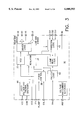
- FIG. 3 is a block diagram of the first embodiment of the present invention.
- FIG. 4 are timing diagrams showing the voltage on the VCO pin, the voltage on the TPH pin and the envelope of load current during normal pre-heat, ignition and running conditions for the first embodiment of the present invention.
- FIG. 5 are timing waveforms showing the voltage on the VCO pin, the voltage on the TPH pin and the envelope of load current during a non-strike condition for the first embodiment of the present invention.
- FIG. 6A-6D are multiple lamp hook-up configurations for the first embodiment of the present invention.
- FIG. 7 is a block diagram of the second embodiment of the present invention.
- FIG. 8 are timing diagrams showing the voltage on the VCO pin, the voltage on the TPH pin and the envelope of load current during normal pre-heat, ignition and dimming conditions for the second embodiment of the present invention.
- FIG. 9 are timing waveforms showing the voltage on the VCO pin, the voltage on the TPH pin and the envelope of load current during a non-strike condition for the second embodiment of the present invention.
- FIG. 10 is a Bode Diagram of the transfer function of the ballast output stage during preheat, ignition and running operating conditions.
- FIG. 11 shows the load current (I L ) during a lamp non-strike occurrence.
- FIG. 12 is a timing diagram during pre-heat of the control circuit of the present invention.
- FIG. 13 shows the closed loop over-current control circuit of the present invention.
- FIG. 14 is a timing diagram of the over-current control circuit of the present invention.
- FIG. 15 is a block diagram of the lamp presence detection circuit of the present invention.
- FIG. 16 are timing waveforms for the lamp presence detection circuit.
- FIG. 17 is a circuit diagram and accompanying truth table for the burst logic of the lamp presence detection circuit.
- FIG. 18 shows the timer circuit of the lamp presence detection circuit.
- FIG. 19 is a timing diagram of the lamp presence detection circuit.
- FIG. 20 is a schematic diagram showing the multiple lamp presence detection circuit in conjunction with a triple parallel lamp configuration and the ballast driver circuit.
- FIG. 21 shows the details of the multiple lamp detection circuit.
- FIG. 22 is a timing diagram of the multiple lamp presence detection circuit.
- FIGS. 23A and 23B show an alternative circuit and timing diagram for the multiple lamp presence detection circuit in which two switches are replaced with an OR gate.
- FIG. 24 shows a traditional lamp resonant circuit.
- FIG. 25 shows the closed-loop pre-heat current control circuit of the present invention.
- FIG. 26 shows a timing diagram of the closed-loop current control circuit of the present invention.
- FIG. 27 shows the analog dimming interface circuit of the present invention.
- FIG. 28 shows the transfer function of the dimming interface circuit of the present invention.
- the first embodiment is a ballast controller IC suitable for multiple lamp configurations.
- the second embodiment is a ballast controller IC which is particularly adapted for low light level dimming.
- FIGS. 1 and 2 the typical connection schematics for the closed-loop ballast ICs of the first and second embodiments of the present invention, respectively, are shown.
- the ballast IC controls two power MOSFETs or IGBTs 20 and 21 connected in a "totem pole", a half-bridge circuit.
- the power MOSFETs/IGBTs 20 and 21 are driven by the ballast controller IC of the present invention to conduct alternatively via gate signals from pins HO and Lo, described below.
- the output circuit which is driven by the power supplied by MOSFETs/IGBTs 20 and 21, includes at least one gas discharge tube, typically a fluorescent lamp 24, which is connected in parallel with a capacitor 26 and in series with an inductor 28 to form a conventional lamp resonant circuit.
- the ballast driver IC of the first embodiment of the invention may be housed in a 16-pin DIP or SOIC package, and has the following pinouts:
- VCC--Logic and internal gate drive supply voltage VCC--Logic and internal gate drive supply voltage.
- a 15.6V internal zener diode clamps the voltage between VCC and GND.
- the nominal rising and falling undervoltage lockout thresholds are TBD and TBD, respectively.
- the total quiescent current is typically less than 150 ⁇ A, reducing the power dissipation requirements for the high voltage startup resistor.
- VCC should be bypassed to GND as close to the IC terminals as possible with a low ESR/ESL capacitor.
- a rule of thumb for the value of this bypass capacitor is to keep its minimum value at least 2500 times the value of the total input capacitance (Ciss) of the power transistors being driven.
- IREF--Reference current setting External resistor sets internal current references for all programmable inputs of IC.
- TPH--Pre-heat timing pin Internal reference current charges an external capacitor up to a 4V threshold to define the pre-heat time.
- IPH--Preheat current setting Internal reference current through an external resistor sets reference for closed-loop peak pre-heat current regulation.
- VCO--Voltage controlled oscillator input External capacitor sets ignition ramp time and loop compensation for pre-heat current and lamp power regulation.
- PLAMP--Lamp Power setting Internal reference current through external resistor sets reference for closed-loop lamp power regulation.
- the COM pin should be connected to the source of the low side power MOSFET using a single, separate board trace, to avoid the possibility of high current ground loops interfering with sensitive timing component currents.
- the ground return path of the timing components and VCC decoupling capacitor should be directly to the IC COM pin, and not via separate traces or jumpers to other ground traces on the board.
- VB--High side gate drive floating supply This is the power supply pin for the high-side level-shifting and gate driver logic circuitry. Power is normally supplied to the high-side circuitry by means of a simple charge pump from VCC.
- a high voltage, fast recovery diode (the so-called bootstrap diode) is connected between VCC (anode) and VB (cathode), and a capacitor (the so-called bootstrap capacitor) is connected between the VB and VS pins.
- the bootstrap capacitor is charged from the VCC-to-COM decoupling capacitor, by means of the bootstrap diode.
- the bootstrap diode When the high-side power MOSFET or IGBT is turned on, the bootstrap diode is reverse-biased, and the VB node floats above the source potential of the high-side power MOSFET or IGBT. VB should be bypassed to VS as close as possible to the IC pins with a low ESR/ESL capacitor. A rule of thumb for the value of this capacitor is to keep its minimum value at least 50 times the value of the total input capacitance (Ciss) of the power transistors being driven.
- This pin is connected to the gate of the high-side power MOSFET or IGBT. If high dV/dt conditions present at the output of the half-bridge cause the power transistor Miller currents (i.e., gate-to-drain currents) to exceed 0.5 A, it is recommended that gate resistors be used to buffer the IC from the power stage.
- VS--High voltage floating supply return The high-side gate driver and logic circuitry returns to this pin.
- the VS pin should be connected directly to the source of the high-side power MOSFET or IGBT.
- the half-bridge output transistors should be placed as close together as possible, in order to minimize series inductance between them.
- LO--Low-Side Gate Driver Output This pin is connected to the gate of the low-side power MOSFET or IGBT. If high dV/dt conditions present at the output of the half-bridge cause the power transistor Miller currents (i.e., gate-to-drain currents) to exceed 0.5 A, it is recommended that gate resistors be used to buffer the IC from the power stage.
- CS1--Universal current sense input Detects voltage produced by load current flowing through external sense resistor which is positive during on-time of either HO or LO gate drive outputs. Also includes a comparator with a lower threshold for detecting lamp presence and an upper threshold for sensing current limit. Also performs current sensing for pre-heat current regulation and for lamp power regulation.
- CS2--Secondary current sense input Detects voltage produced by load current flowing through external sense resistor which is positive during on-time of HO gate drive output. Includes a window comparator with a low threshold for detecting lamp presence and an upper threshold for detecting current limit.
- CS3--Third current sense input Detects voltage produced by load current flowing through external sense resistor which is positive during on-time of HO gate drive output. Includes a window comparator with a lower threshold for detecting lamp presence and an upper threshold for current limit.
- SD--Shutdown Pin This pin is used to disable the half-bridge driver circuitry, turning both of the gate driver outputs HO and LO off (active low), and putting the ballast IC controller into the micropower mode.
- the rising shutdown pin threshold voltage is 2.5V, and approximately 0.1V of hysteresis has been included to increase noise immunity.
- the shutdown function is not latched, and the output of the SD comparator resets the CS latch, so that when the SD pin voltage is brought back below its input threshold the IC reinitiates the preheat sequence.
- VCO voltage-controlled oscillator
- REGULATION the "REGULATION" block 34, which sources or sinks current into a capacitor (not shown) at the input of VCO 32, depending on the error between a reference phase and the phase of the inductor current of one of the resonant lamp output stages.
- the inductor current is sensed by a voltage at one of the current-sensing inputs (CS1, CS2 or CS3) which is produced by inserting a sensing resistor (RCS) 36 between the lamp filament and ground (as shown in the typical connection diagram of FIG. 2) and/or between the source of the lower half-bridge MOSFET 21 and ground.
- RCS sensing resistor
- the REGULATION block 34 is used to regulate the peak, cycle-by-cycle load current against a programmable pre-heat current reference input, IPH.
- Preheat logic is included in block 40--the pre-heat time is determined by a linear ramping voltage produced by an internal current charging an external capacitor on pin TPH. If the lamp does not strike, the ballast deactivates as shown in the timing diagram of FIG. 5.
- Lamp power is set by a voltage produced by an internal current flowing through an external resistor at pin PLAMP, which sets the reference phase for phase control block 38.
- An internal current through an external resistor at pin EOL produces a voltage which, when compared with the VCO voltage, programs a maximum frequency shutdown. If end-of-life occurs in one or more of the lamps as detected by protection logic 40, phase control 38 causes the frequency to increase in an attempt to keep the power constant until the maximum frequency, FMAX, is reached and the ballast is safely shut down.
- the shutdown pin, SD provides a logic input external shutdown option. If this pin is pulled above 2 volts, the ballast is held off in an ⁇ un-latched ⁇ state. When pulled back below 2 volts again, the preheat sequence is reset via preheat logic 42, and the ballast starts again. This allows for automatic restarting of the ballast after a fault condition has occurred by removing and inserting a lamp without recycling the input mains voltage to the ballast.
- FIGS. 6A-6D show various multiple lamp configurations for the ballast controller IC of the first embodiment of the invention--FIG. 6A shows a dual parallel configuration; FIG. 6B shows a dual series configuration; FIG. 6C shows a triple parallel configuration; and FIG. 6D shows a series-parallel configuration.
- the sense resistor(s) RCS1-RCS3 for multiple lamp configurations are disposed between the lamp cathodes and ground; similarly, RCS 36 in FIG. 1, a single lamp configuration, could be inserted in this alternative position.
- the ballast controller IC of the present invention also includes, as depicted in circuit block 44, micro-power start-up, zener clamped VCC, over-temperature shutdown and under-voltage lockout.
- the under-voltage lockout (UVLO) provides turn-on and turn-off thresholds with hysteresis for noise and off-line supply.
- the overall architecture of the second embodiment of the ballast IC controller of the present invention differs from that of the first embodiment in that it is specifically designed for professional dimming down to ultra-low light levels.
- the chip of the second embodiment shown in FIG. 2 and identified by reference numeral 50, has many of the same pinouts as the first embodiment, with the following exceptions relating to the dimming function:
- VCO--Voltage controlled oscillator input External capacitor sets not only ignition ramp time and loop compensation for pre-heat current regulation, but also phase control for dimming.
- DIM--Dimming control input 0-5VDC external control voltage corresponding to lamp power setting.
- MAX--Maximum lamp power Internal reference current through external resistor sets maximum lamp power corresponding to 5VDC dimming control input voltage.
- CS--Current sense input Detects the voltage produced by load current flowing through external sense resistor which is positive during on-time of LO gate drive output. Includes a comparator with upper threshold for current limit. Also performs current sensing for pre-heat current regulation and for phase control (dimming).
- the resistor between pin FB and pin VCO has a value of between 500 ⁇ -10 K ⁇ .
- a DIMMING INTERFACE 52 which allows 0-5VDC analog control of lamp brightness, with minimum and maximum adjustments.
- an IGNITION DETECTION block 54 detects a change in the phase of the inductor current (as measured in the source of the lower half-bridge MOSFET at PIN CS) indicative of a lamp ignition. This tells the REGULATION block 34 that the lamp has successfully ignited and to close-the-loop and regulate the phase of the inductor current against the reference phase generated by the DIM INTERFACE 52.
- an internal switch S1 is provided to connect the DIM input to the TPH pin, which ramps up to between 4 and 5 volts during ignition.
- capacitor 58 connected to pin TPH, charges up through an internal current source during preheat. When the voltage on capacitor 58 reaches the 4V internal threshold, preheat is over. With continuing reference to FIG. 8, capacitor 58 continues to charges past 4V, the lamp ignites, and the ignition detection block 54 detects ignition. At this point, the circuitry of the chip closes switch S1 (FIG. 7) and the voltage on the DIM pin discharges to the voltage set by the user at an exponential rate determined by values of capacitor 58 and resistor 56.
- Capacitor 58 typically has a maximum value of 1 ⁇ F and resistor 56 has a typical value between 1 K-100 K ⁇ , depending on the desired travel time.
- Both embodiments of the invention have over-current protection defined by an internal threshold generated within protection logic block 40.
- the protection compares an internal threshold with the voltage developed across a low-ohmic external current sensing resistor RCS through pin CS (pins CS1, CS2 and CS3 in the first embodiment).
- External current sensing resistor RCS is disposed between the lower half-bridge switch and ground (as shown, for example in FIGS. 1 and 2) or disposed between the lower lamp filament and ground (as shown, for example, in FIGS. 6A and 6C).
- the peak output current is first regulated or limited to the threshold by injecting current pulses to the VCO capacitor via a signal to Phase Control 38 each time the threshold is exceeded. (Note that the direction in which the VCO is designed to operate is arbitrary--i.e., the circuit could be designed such that the VCO capacitor is sinked by current pulses, rather than charged.) This continues until pin TPH voltage charges up to 5V, allowing the lamp to strike. The next time the threshold is exceeded, the ballast IC is latched off and the half-bridge switches are tri-stated, shutting the ballast down.
- the over-current threshold can be used to detect non-zero voltage at the half-bridge, which can occur when the lamp is removed, as described in greater detail in the following section on the lamp presence detection circuit.
- the overcurrent protection circuit of the present invention which is responsible for sensing the current, regulating the current against a reference threshold and tri-stating the half-bridge switches, is shown in FIG. 13, with the corresponding timing diagram shown in FIG. 12 aligned with appropriate load current in FIG. 11.
- the Bode diagram of the transfer function of the resonant output stage (FIG. 10) shows the operating points of the ballast, together with the current limit. As shown in FIG. 10, the current is limited at the threshold for a fixed time before the half-bridge switches are tri-stated (both off). Maintaining the current for some time before the ballast is shutdown will give the lamp time to ignite.
- the circuit compares a voltage proportional to the total load current across RCS with a fixed threshold V IMAX .
- V IMAX the output of COMP1 (FB) goes high and sends a pulse to switch S1.
- the voltage on C VCO therefore increases, causing the output frequency of the half-bridge signal driving the lamp resonant stage (VS) to also increase. This moves the operating point along the High-Q transfer function (FIG. 10) to the right, decreasing the total load current below the maximum limit.
- the same circuit is used for regulating the peak pre-heat current flowing through the lamp filaments.
- the peak current reference threshold is initially connected to V IPH (FIG. 13) via switch S2 and regulates the total peak load current to this value until the voltage on capacitor CPH exceeds threshold voltage V OCP .
- the pre-heat period has ended (see FIGS. 11 and 12) and the output of comparator COMP3 drives switch S2 to the "high" position (as denoted by a "1" on S2), shifting the regulation threshold to the higher value V IMAX .
- Current source I2 discharges capacitor C VCO linearly, causing the frequency to ramp down towards the resonance frequency of the High-Q resonant output stage (FIG. 10) until either the lamp strikes successfully, or, V IMAX is reached.
- FIG. 14 is a timing diagram of the over-current control circuit of FIG. 13.
- the first embodiment of the invention includes not only an upper threshold, but also a lower threshold of 200mV which is used to detect near or below resonance operation and lamp insertion during running.
- Both embodiments of the invention include lamp presence detection circuitry to detect: (1) if a fluorescent lamp (or lamps) have been inserted into the lamp resonant circuit before starting up; and (2) if a fluorescent lamp is removed during ballast operation.
- This circuitry avoids damage to the ballast, specifically to MOSFETs/IGBTs 20 and 21, which can occur if ballast continues to operate during a lamp out condition. The damage is caused by high currents resulting from the charging or discharging of snubber capacitor 60 (see FIGS.
- the lamp presence detection circuit of the present invention contained within Protection Logic block 40, uses the same sense resistor RCS described above with respect to peak current detection, disposed in series with the source of the lower MOSFET/IGBT 21 of the half-bridge.
- the current flowing through resistor RCS is zero if the half-bridge is operating with no lamp inserted, except for the high current "spikes" which occur at the turn-on of MOSFET/IGBT 21.
- resistor RCS which is only present when MOSFET/IGBT 21 is on, which is a piece-wise-linear section of the total lamp circuit current (I L1 ), and is 90° phase shifted from the total lamp circuit current (I L1 ) (see FIG. 16).
- the resulting voltage across resistor RCS is compared with a d.c. threshold voltage "th" (COMP1) (FIG. 15) with the output being a digital ⁇ high ⁇ if the voltage across RCS is greater than ⁇ Vth ⁇ and a digital ⁇ low ⁇ if the voltage across RCS is less than ⁇ Vth ⁇ .
- comparator COMP1 Due to the slow rising edge of the current being measured, it is possible for the comparator output to "chatter” as the voltage across resistor RCS begins to exceed “Vth". To avoid detection of this "chatter” or any other unwanted signals such as turn-on "spikes” or high frequency, high-current noise which can be present on the measuring point (voltage over RCS), the output of comparator COMP1 is synchronized with the turn-off edge of MOSFET/IGBT 21. This is accomplished with a D-Type Flip Flop (DFF1, FIG.
- DFF1 D-Type Flip Flop
- the output of DFF1 (LAMPIN) is then a digital ⁇ high ⁇ for a lamp in and a digital ⁇ low ⁇ for a lamp out and is an input to a Burst Logic Block (FIG. 15) whose circuit is shown in greater detail in FIG. 17.
- This Burst Logic Block outputs a ⁇ Start ⁇ and ⁇ Reset ⁇ signal to a Timer Block, which, in turn, outputs a signal ⁇ Enable ⁇ to the Driver Logic Block.
- the Burst Logic and Timer function together such that an internal clock ( ⁇ 500 Hz) (CLK1) signal (see FIG. 19) is divided out five times until an interval of about 16 Hz is achieved.
- ⁇ Enable ⁇ goes ⁇ high ⁇ , enabling the Driver Logic to drive the Half-Bridge Driver and therefore MOSFETs/IGBTs 20 and 21 accordingly.
- ⁇ Setdet ⁇ goes ⁇ high ⁇ , instructing the Burst Logic to read signal ⁇ Lampin ⁇ . If ⁇ Lampin ⁇ is ⁇ high ⁇ , then a lamp presence is detected and the system continues operating.
- ⁇ Start ⁇ signal goes ⁇ high ⁇ which latches both the ⁇ Setdet ⁇ and ⁇ Enable ⁇ signals ⁇ high ⁇ and the pre-heat interval of the Timer block begins (see FIG. 18 for Timer circuit).
- ⁇ Lampin ⁇ is instead ⁇ low ⁇ when ⁇ Setdet ⁇ goes ⁇ high ⁇
- the ⁇ Reset ⁇ signal goes high and resets the Timer.
- the Timer is reset the ⁇ Enable ⁇ goes ⁇ low ⁇ and the half-bridge driver turns off, therefore turning MOSFETs/IGBTs 20 and 21 off.
- ⁇ Enable ⁇ goes ⁇ low ⁇ , it also frees the latch on ⁇ Setdet ⁇ , which then goes low.
- the lamp presence detection circuit will read ⁇ Lampin ⁇ signal as ⁇ low ⁇ and go into burst mode until a new lamp is inserted. Furthermore, should the end of life phenomenon of the lamp known as the ⁇ rectifying effect ⁇ occur, where one cathode breaks but the other cathode continues to emit, the current flowing through resistor ⁇ RCS ⁇ goes asymmetrical and below ⁇ Vth ⁇ therefore turning the MOSFETs/IGBTs 20 and 21 off and the system goes into the burst mode.
- the first embodiment of the ballast driver IC of the present invention which is adapted to drive multiple fluorescent lamps, advantageously includes multiple lamp presence detection circuitry.
- the multiple lamp presence detection circuit detects the presence of each individual lamp and regulates the lamp power in one of them. If the regulated lamp is removed during running, the circuit searches for the next available lamp to regulate. If the removed lamp is reinserted during running, the ballast control circuit disables the half-bridge transistor switches 20 and 21, and resets the pre-heat sequence before starting again. If all lamps are removed from the lamp resonant output circuit (see FIGS. 6A-6D), the half-bridge driver 30 is disabled and both half-bridge switches 20 and 21 turn off.
- a sense resistor (RCS1, RCS2, RCS3) is disposed between each lamp filament and ground to detect the total current of each lamp resonant circuit. If any lamp filament is removed then the voltage over the sense resistor in that path V RCS1 , V RCS2 , V RCS3 goes to zero.
- V th1 a low threshold voltage
- comparators 70, 71, 72, and measuring just before the gate drive signal HO turns the upper half-bridge switch 20 off by clocking a D-Type Flip Flop 73, 74, 75 with HIN (see circuit diagram, FIG. 21, and timing diagram, FIG. 22), a signal is generated which is indicative of a complete circuit in each lamp resonant circuit and therefore of all lamp cathodes intact and inserted in the circuit.
- Each current sense input is clocked with HIN since the current flow direction through each sense resistor is at its peak when the upper half-bridge switch 20 turns off. This blanks out all other unwanted current spikes and/or noise which may be present at other times during the switching period.
- the Q outputs from the D Flip Flops 73, 74, 75 are then NOR-ed together (in NOR gate 76) to form signal LMPN, which goes ⁇ high ⁇ only if all lamp resonant circuits do not have a complete circuit (all lamps removed or all have broken cathodes) and the ballast control latches the half-bridge switches 20 and 21 off. If a single lamp is removed and reinserted, the appropriate pulse generator gives a reset pulse LIDO (Lamp Inserted During Operation) when the lamp is reinserted and the ballast control turns the half-bridge switches off, resets the pre-heat sequence, and restarts the ballast control again. This is to prevent ⁇ hard-striking ⁇ of the inserted lamp and possible damage to the half-bridge transistor switches 20 and 21 as a result of the running frequency being lower than the resonance frequency of the High-Q series LC combination formed when a lamp is reinserted.
- LIDO Read Inserted During Operation
- the zero-crossing (ZX) of the total load current is required from one of the lamp resonant circuits with a good lamp inserted. If the lamp which is being regulated is removed, the voltage-controlled switches (S1 and S2), controlled by the signals indicative of a lamp presence (i.e., by the outputs of D flip flops 73, 74), form a ⁇ lamp search ⁇ circuit which uses the process of elimination to find the next available lamp to regulate. If all lamps are present then the lamp connected to CS1 is regulated. If CS1 has no lamp connected, then the zero-crossing of CS2 is regulated. If both CS1 and CS2 have no lamp connected then the zero-crossing of CS3 is regulated (see the following Truth Table):
- switches S1 and S2 With a 3-input OR-gate as shown in FIG. 23A.
- the phase measurement (zero-crossing detection) of the resonant output stage lamp with the smallest phase-shift with respect to the half-bridge voltage will determine the pulse width of signal ZX (see FIG. 23B). This means that the lamp drawing the most power will be the master and be regulated, while the others will be the slaves and follow close by. This eliminates the need to jump to the next available lamp when the master lamp is removed and simplifies the circuit.
- a closed-loop solution can be used which adjusts the pre-heat frequency continuously while keeping the pre-heat current constant. Furthermore, closing the loop also allows for a simpler oscillator circuit with larger tolerances rather than with open-loop circuits which require tighter tolerance specifications.
- Closing the loop requires ⁇ feeding back ⁇ a measurement of the cathode current and comparing it against a current setting or ⁇ reference ⁇ .
- the result is usually called the ⁇ error ⁇ , which is used to adjust the system until the reference equals the feedback and the error is zero.
- the system is then independent of outside influences such as component tolerances, voltage fluctuations and temperature.
- the closed-loop pre-heat current control circuit for an electronic ballast of the present invention uses the same classical approach described above, but the implementation and control circuitry is new and unique.
- the pre-heat cathode current is sensed in the source of MOSFET/IGBT 21 (see FIG. 25) as the voltage drops across RCS (V FB ).
- This signal is the total lamp resonant circuit current (I L ), only 90° phase shifted (FIG. 26) due to the direction of current flow through sense resistor RCS with respect to the direction of current flow through the resonant circuit (I L ).
- Voltage V FB is then compared with a reference voltage ⁇ REF ⁇ through comparator ⁇ COMP1 ⁇ , with the output ⁇ ERROR ⁇ being the associated error between the ⁇ V FB ⁇ and ⁇ REF ⁇ .
- the resulting associated error ⁇ pulse ⁇ , ⁇ ERROR ⁇ drives an amplifier comprised of MOSFETs 78 and 79 which charges or discharges (depending on whether ⁇ V FB ⁇ is greater than or less than) capacitor C2 with fixed current sources CHARGE and I REF DISCHARGE.
- the resulting voltage over capacitor C2, ⁇ V VCO ⁇ then steers a voltage controlled oscillator to a higher or lower frequency, depending on whether ⁇ V FB ⁇ is greater than or less than ⁇ REF ⁇ , at a fixed duty cycle of 50%.
- the resulting signal is then used to drive a ⁇ half-bridge driver ⁇ circuit at the desired frequency which then drives MOSFETs/IGBTs 20 and 21.
- the resulting high-voltage square-wave voltage ⁇ VS ⁇ (FIG. 26) is the input to the lamp resonant output circuit which outputs a current that is a function of the frequency and amplitude of voltage ⁇ VS ⁇ .
- the total lamp resonant circuit current (I L ) is equal to the current flowing in the lamp cathodes and capacitor C (FIG. 25). This is due to the fact that during pre-heat, the lamp has not yet ignited and the circuit is an under-damped, series RCL configuration, with the lamp cathodes being connected in series with L and C.
- a more classical approach to regulating the current would be to sense the current out at the load with a transformer, full wave rectify the output, and low-pass filter the rectified voltage to get a DC voltage representation of the current. This DC voltage would then be summed together with a DC reference voltage through an error amplifier of a limited bandwidth and a given compensation network. The resulting error would then steer a VCO.
- This method has a high component count, and, the rectification of the transformer voltage (as well as the voltage drop across the rectifying diodes vs. temperature) is a non-linear operation which can give errors.
- the current control circuit of the present invention greatly simplifies the measurement and summing operations, has fewer components and is linear.
- the preheat current control circuit of the present invention simply converts the current to reference error directly to a time. This time controls how long a constant current flows into or out of a capacitor. The resulting voltage over the capacitor C2 is already in its integrated form, as given by ##EQU1##
- a dimmable electronic ballast such as the second embodiment of the present invention, it is necessary to trim the minimum and maximum brightness settings to within an allowable tolerance range such that uniform brightness is achieved with multiple ballasts. This is especially necessary at low brightness levels, where small deviations in brightness from one lamp to another are easily detectable with the human eye.
- the dimming interface circuit of the present invention converts an analog input control voltage to an analog output reference voltage with programmable offset and gain adjustments for trimming. Because some fluorescent lamp types are dimmed to lower light levels than others depending on the application, the dimming interface of the present invention allows for universal trimming to any minimum and maximum brightness level (or lamp power) to accommodate all lamp types.
- the dimming interface circuit of the present invention advantageously provides independent control of the MIN and MAX settings.
- the input voltage is at the DIM node and op amp 80 regulates the minus (-) terminal to DIM input voltage.
- a second voltage controlled current source is given by op amp 81, Q2, R MIN and V REF1 , where R MIN (with V REF1 constant) controls the gain of I MIN .
- I DIM and I MIN are then summed together at node ⁇ to give the mathematical expression: ##EQU2## therefore giving independent control of gain and offset. (FIG. 28).
- the resulting current is then mirrored through current mirror R1, R2, Q3 and Q4 before flowing through R3 to produce voltage V 93 .
- R3 is an external resistor then the circuit would be complete and tolerances due to temperature effects would be acceptable. If the current is to be all internal to the IC, with the exception of programmable resistors R MAX and R MIN , then the resistance of R3 must not change dramatically with temperature, and, for example, an additional unity gain buffer (op amp 83, Q5, R4) and current mirrors (R5, R6, Q6, Q7 and R7, R8, Q8 and Q9) can be implemented to achieve further conversions (FIG. 2).
- op amp 83, Q5, R4 and current mirrors R5, R6, Q6, Q7 and R7, R8, Q8 and Q9
- the novelty of the circuit of the present invention resides in summing two independent currents, each controlled by a voltage and a resistor, to form an end analog function of the form:
- R3 is internal to the IC, then it must have a zero temperature coefficient so that the end reference does not change with temperature.
Abstract
Description
              TRUTH TABLE
______________________________________
           FF 73  FF 14  FF 75
Lamps Present
            OUT     OUT      OUT
                              ZX          CONDITION
______________________________________
NONE       0      0      0    0      LMPN `HIGH`,
                                       BALLAST OFF
LAMP1                 0          COMP 70
                                       LAMP1 POWER
                                  OUT
                                       REGULATED
LAMP2                 1          COMP 71
                                       LAMP2 POWER
                                  OUT
                                       REGULATED
LAMP1 & LAMP2
            0         1          COMP 70
                                       LAMP1 POWER
                                  OUT
                                       REGULATED
LAMP3                 0          COMP 72
                                       LAMP3 POWER
                                  OUT
                                       REGULATED
LAMP1 & LAMP3
            1         0          COMP 70
                                       LAMP1 POWER
                                  OUT
                                       REGULATED
LAMP2 & LAMP3
            1         1          COMP 71
                                       LAMP2 POWER
                                  OUT
                                       REGULATED
ALL                   1    1     COMP 70
                                       LAMP1 POWER
                                  OUT
                                           REGULATED
______________________________________
y=ms+b.
Claims (14)
Priority Applications (1)
| Application Number | Priority Date | Filing Date | Title |
|---|---|---|---|
| US09/022,554 US6008593A (en) | 1997-02-12 | 1998-02-12 | Closed-loop/dimming ballast controller integrated circuits |
Applications Claiming Priority (6)
| Application Number | Priority Date | Filing Date | Title |
|---|---|---|---|
| US3792497P | 1997-02-12 | 1997-02-12 | |
| US3792697P | 1997-02-12 | 1997-02-12 | |
| US6186297P | 1997-10-15 | 1997-10-15 | |
| US6184697P | 1997-10-15 | 1997-10-15 | |
| US7048498P | 1998-01-05 | 1998-01-05 | |
| US09/022,554 US6008593A (en) | 1997-02-12 | 1998-02-12 | Closed-loop/dimming ballast controller integrated circuits |
Publications (1)
| Publication Number | Publication Date |
|---|---|
| US6008593A true US6008593A (en) | 1999-12-28 |
Family
ID=27534642
Family Applications (1)
| Application Number | Title | Priority Date | Filing Date |
|---|---|---|---|
| US09/022,554 Expired - Lifetime US6008593A (en) | 1997-02-12 | 1998-02-12 | Closed-loop/dimming ballast controller integrated circuits |
Country Status (2)
| Country | Link |
|---|---|
| US (1) | US6008593A (en) |
| DE (1) | DE19805733A1 (en) |
Cited By (80)
| Publication number | Priority date | Publication date | Assignee | Title |
|---|---|---|---|---|
| WO2000078678A2 (en) * | 1999-06-21 | 2000-12-28 | Amway Corporation | Fluid treatment system with electromagnetic radiation |
| US6172466B1 (en) * | 1999-02-12 | 2001-01-09 | The Hong Kong University Of Science And Technology | Phase-controlled dimmable ballast |
| US6218788B1 (en) * | 1999-08-20 | 2001-04-17 | General Electric Company | Floating IC driven dimming ballast |
| US6326740B1 (en) | 1998-12-22 | 2001-12-04 | Philips Electronics North America Corporation | High frequency electronic ballast for multiple lamp independent operation |
| WO2001097572A1 (en) * | 2000-06-12 | 2001-12-20 | Matsushita Electric Works, Ltd. | Electronic ballast for a discharge lamp |
| WO2001098853A1 (en) * | 2000-06-19 | 2001-12-27 | International Rectifier Corporation | Ballast control ic with minimal internal and external components |
| US6366032B1 (en) * | 2000-01-28 | 2002-04-02 | Robertson Worldwide, Inc. | Fluorescent lamp ballast with integrated circuit |
| WO2002033502A1 (en) * | 2000-10-20 | 2002-04-25 | International Rectifier Corporation | Ballast control ic with power factor correction |
| WO2002041669A2 (en) * | 2000-11-16 | 2002-05-23 | Koninklijke Philips Electronics N.V. | Voltage regulated electronic ballast for mutliple discharge lamps |
| US6414449B1 (en) * | 2000-11-22 | 2002-07-02 | City University Of Hong Kong | Universal electronic ballast |
| EP1227707A2 (en) * | 2001-01-23 | 2002-07-31 | Patent-Treuhand-Gesellschaft für elektrische Glühlampen mbH | Microcontroller, switch-mode power supply and electronic ballast for operating at least one lamp |
| US6436299B1 (en) | 1999-06-21 | 2002-08-20 | Amway Corporation | Water treatment system with an inductively coupled ballast |
| US6476567B1 (en) * | 1999-03-31 | 2002-11-05 | Innoware Oy | Control gear for fluorescent lamps |
| EP1265347A2 (en) * | 2001-06-08 | 2002-12-11 | Grundfos A/S | Bootstrap voltage supply |
| WO2003019993A1 (en) * | 2001-08-27 | 2003-03-06 | Koninklijke Philips Electronics N.V. | Circuit arrangement |
| WO2003059017A1 (en) * | 2001-12-31 | 2003-07-17 | International Rectifier Corporation | Basic halogen convertor ic |
| US20030173906A1 (en) * | 2002-03-18 | 2003-09-18 | Weon-Ho Lee | Energy-saving dimming apparatus |
| US6673250B2 (en) | 1999-06-21 | 2004-01-06 | Access Business Group International Llc | Radio frequency identification system for a fluid treatment system |
| US20040007992A1 (en) * | 2002-07-09 | 2004-01-15 | International Rectifier Corporation | Adaptive ballast control IC |
| US20040012347A1 (en) * | 2002-07-22 | 2004-01-22 | International Rectifier Corporation | Single chip ballast control with power factor correction |
| US20040056610A1 (en) * | 2002-09-25 | 2004-03-25 | Gilbert Fregoso | Circuit for driving cold cathode tubes |
| US20040113662A1 (en) * | 2002-12-11 | 2004-06-17 | Grimsrud Knut S. | Presence indication signal associated with an attachment |
| WO2004066675A2 (en) * | 2003-01-16 | 2004-08-05 | International Rectifier Corporation | Dimming ballast control ic with flash suppression circuit |
| US6777942B2 (en) * | 2000-09-27 | 2004-08-17 | Patent-Treuhand-Gesellschaft Fuer Elektrische Gluehlampen Mbh | Operating device for gas discharge lamps with detection of filament breakage |
| US20040232855A1 (en) * | 2003-05-05 | 2004-11-25 | Ribarich Thomas J. | Digital electronic ballast control apparatus and method |
| US6853154B2 (en) * | 2002-04-30 | 2005-02-08 | Koninklijke Philips Electronics N.V. | Open loop bi-level ballast control |
| US6900599B2 (en) * | 2001-03-22 | 2005-05-31 | International Rectifier Corporation | Electronic dimming ballast for cold cathode fluorescent lamp |
| US20050116744A1 (en) * | 2003-11-28 | 2005-06-02 | Mitsubishi Denki Kabushiki Kaisha | Inverter circuit |
| DE102004009006A1 (en) * | 2003-12-11 | 2005-07-14 | Conti Temic Microelectronic Gmbh | Method for functional testing of a lamp circuit |
| US20050156534A1 (en) * | 2004-01-15 | 2005-07-21 | In-Hwan Oh | Full digital dimming ballast for a fluorescent lamp |
| US20050184682A1 (en) * | 2004-02-19 | 2005-08-25 | International Rectifier Corporation | Ballast dimming control IC |
| US20050225265A1 (en) * | 2004-04-08 | 2005-10-13 | International Rectifier Corporation | PFC and ballast control IC |
| US20050253534A1 (en) * | 2004-05-11 | 2005-11-17 | Design Rite Llc | Circuit for driving cold cathode tubes and external electrode fluorescent lamps |
| EP1599775A2 (en) * | 2003-03-03 | 2005-11-30 | International Rectifier Corporation | Digital lighting ballast oscillator |
| US20050269972A1 (en) * | 2005-03-31 | 2005-12-08 | Trestman Grigoriy A | Ballast with end-of-lamp-life protection circuit |
| US20060006812A1 (en) * | 2004-07-07 | 2006-01-12 | Osram Sylvania Inc. | Resonant inverter including feed back circuit with source of variable bias current |
| EP1624731A2 (en) * | 2004-08-02 | 2006-02-08 | Infineon Technologies AG | Circuit with monitoring function for a fluorescent lamp, and method for monitoring a fluorescent lamp |
| US20060087249A1 (en) * | 2004-10-21 | 2006-04-27 | Patent-Treuhand-Gesellschaft Fur Elektrisch Gluhlampen Mbh | Lamp operating circuit and operating method for a lamp having active current measurement |
| US7045966B2 (en) | 2004-07-07 | 2006-05-16 | Osram Sylvania Inc. | Resonant inverter including feed back circuit having phase compensator and controller |
| US20060181224A1 (en) * | 2005-02-16 | 2006-08-17 | Neil Gibson | Method and device for controlling the light intensity in a multi-lamp illumination device for a display panel |
| US7095183B2 (en) | 2004-07-07 | 2006-08-22 | Osram Sylvania Inc. | Control system for a resonant inverter with a self-oscillating driver |
| US20060186834A1 (en) * | 2004-02-11 | 2006-08-24 | International Rectifier | Multiple lamp ballast control circuit |
| US20060244624A1 (en) * | 2002-12-16 | 2006-11-02 | Ling Wang | System and method for lighting control network recovery from master failure |
| US20060279234A1 (en) * | 2005-06-08 | 2006-12-14 | Logah Technology Corp. | Phase sampling protection device |
| US20070085488A1 (en) * | 2005-10-12 | 2007-04-19 | Thomas Ribarich | Dimmable ballast control integrated circuit |
| EP1776749A2 (en) * | 2004-02-19 | 2007-04-25 | International Rectifier Corporation | Half bridge adaptive dead time circuit and method |
| US20070090775A1 (en) * | 2005-10-24 | 2007-04-26 | Ribarich Thomas J | Dimming ballast control circuit |
| US20070090774A1 (en) * | 2005-10-25 | 2007-04-26 | Hon Hai Precision Industry Co., Ltd. | Discharge lamp driving device and driving method |
| US20070103089A1 (en) * | 2005-05-11 | 2007-05-10 | Gilbert Fregoso | Circuit for driving cold cathode tubes and external electrode fluorescent lamps |
| US20070130011A1 (en) * | 1999-06-23 | 2007-06-07 | Signature Systems Llc | System for electronic barter, trading and redeeming points accumulated in frequent use reward programs |
| US20070145907A1 (en) * | 2005-12-02 | 2007-06-28 | Jong-Tae Hwang | Ballast integrated circuit (IC) |
| US20070252534A1 (en) * | 2006-04-27 | 2007-11-01 | Onn Fah Foo | Light Control Fluorescent Lamp And Circuit Thereof |
| US20080061791A1 (en) * | 2003-12-11 | 2008-03-13 | Conti Temic Microelectronic, Gmbh | Procedure for Testing the Function of a Lamp Circuit |
| WO2008119613A1 (en) * | 2007-03-30 | 2008-10-09 | Osram Gesellschaft mit beschränkter Haftung | Method of ignition regulation of discharge lamp and the corresponding electronic ballast circuit |
| US20080284350A1 (en) * | 2007-05-17 | 2008-11-20 | Jian Xu | Bulb type detector for dimmer circuit and inventive resistance and short circuit detection |
| US20080309256A1 (en) * | 2007-06-15 | 2008-12-18 | System General Corp. | Integrated circuit controller for ballast |
| US20080315787A1 (en) * | 2007-06-19 | 2008-12-25 | Jian Xu | Dimming algorithms based upon light bulb type |
| WO2009047174A1 (en) * | 2007-10-08 | 2009-04-16 | Osram Gesellschaft mit beschränkter Haftung | Circuit and method for double peak current control |
| US20090195161A1 (en) * | 2004-09-28 | 2009-08-06 | Acuity Brands, Inc. | Equipment and methods for emergency lighting that provides brownout detection and protection |
| US20090224692A1 (en) * | 2008-03-04 | 2009-09-10 | Dong-Hun Lee | Inverter Driver and Lamp Driver Using the Same |
| US20090256481A1 (en) * | 2008-04-11 | 2009-10-15 | Osram Sylvania Inc. | Stand alone lamp filament preheat circuit for ballast |
| US20100188134A1 (en) * | 2008-12-30 | 2010-07-29 | Stmicroelectronics S.R.L | Control of a resonant switching system with monitoring of the working current in an observation window |
| US20100238047A1 (en) * | 2009-03-20 | 2010-09-23 | Lutron Electronics Co., Inc. | Method of Confirming that a Control Device Complies with a Predefined Protocol Standard |
| US20110199710A1 (en) * | 2010-02-16 | 2011-08-18 | Mitsubishi Electric Corporation | Semiconductor device |
| US20120062137A1 (en) * | 2004-08-02 | 2012-03-15 | Infineon Technologies Ag | Method for Detection of Non-Zero-Voltage Switching Operation of a Ballast of Fluorescent Lamps, and Ballast |
| CN102474967A (en) * | 2009-08-07 | 2012-05-23 | 欧司朗股份有限公司 | Method for actuating a discharge lamp and circuitry for operating such a lamp |
| CN101094551B (en) * | 2006-06-23 | 2012-07-04 | 电灯专利信托有限公司 | Method of detecting BJT cut-off signals in electronic ballast and electronic ballast |
| US20120242240A1 (en) * | 2011-03-25 | 2012-09-27 | Cornelis Jozef Petrus Maria Rooijackers | Ballast efficiency improvement for fluorescent lamps |
| CN102782843A (en) * | 2010-02-03 | 2012-11-14 | 本田技研工业株式会社 | Semiconductor device |
| US8378579B1 (en) | 2010-02-18 | 2013-02-19 | Universal Lighting Technologies, Inc. | Ballast circuit for a gas discharge lamp with a control loop to reduce filament heating voltage below a maximum heating level |
| US20130293131A1 (en) * | 2008-02-08 | 2013-11-07 | Laurence P. Sadwick | Solid State Semiconductor LED Replacement for Fluorescent Lamps |
| CN103390990A (en) * | 2013-07-24 | 2013-11-13 | 深圳市开立科技有限公司 | Isolating conversion circuit of power supply |
| US20130300308A1 (en) * | 2012-05-12 | 2013-11-14 | Laurence P. Sadwick | Current Limiting LED Driver |
| US20140167640A1 (en) * | 2012-12-18 | 2014-06-19 | Dialog Semiconductor Gmbh | Back-up Capacitor |
| US20140265900A1 (en) * | 2013-03-15 | 2014-09-18 | Laurence P. Sadwick | Fluorescent Lamp LED Replacement |
| US8947020B1 (en) * | 2011-11-17 | 2015-02-03 | Universal Lighting Technologies, Inc. | End of life control for parallel lamp ballast |
| US9041293B2 (en) | 2011-12-27 | 2015-05-26 | Industrial Technology Research Institute | Lamp control system, lamp power-saving system and method therefor |
| TWI602396B (en) * | 2012-12-21 | 2017-10-11 | 微晶片科技公司 | Mains voltage zero-crossing detector, microcontroller comprising the same and method for detecting mains voltage zero-crossing |
| CN110286505A (en) * | 2019-06-14 | 2019-09-27 | 深圳市全洲自动化设备有限公司 | A kind of automatic search foot position method and system applied to LCD white glass AOI test |
| EP4071991A1 (en) * | 2021-04-08 | 2022-10-12 | Silergy Semiconductor Technology (Hangzhou) Ltd | Control circuit, control method and resonant converter |
Families Citing this family (3)
| Publication number | Priority date | Publication date | Assignee | Title |
|---|---|---|---|---|
| DE19928042A1 (en) * | 1999-06-18 | 2000-12-21 | Patent Treuhand Ges Fuer Elektrische Gluehlampen Mbh | Method for operating at least one fluorescent lamp and electronic ballast therefor |
| GB9923389D0 (en) * | 1999-10-05 | 1999-12-08 | Central Research Lab Ltd | A high frequency power oscillator |
| DE102008031409A1 (en) * | 2008-07-02 | 2010-01-07 | Tridonicatco Gmbh & Co. Kg | Detection of the type of a gas discharge lamp connected to an operating device |
Citations (19)
| Publication number | Priority date | Publication date | Assignee | Title |
|---|---|---|---|---|
| JPS62249398A (en) * | 1986-04-23 | 1987-10-30 | キヤノン株式会社 | Radio frequency fluorescent lamp lighting apparatus |
| JPH0242396A (en) * | 1988-08-03 | 1990-02-13 | Toshiba Corp | Radioactive material transport container |
| JPH02148595A (en) * | 1988-11-30 | 1990-06-07 | Nec Corp | Thin film el device and manufacture thereof |
| JPH02199797A (en) * | 1989-01-26 | 1990-08-08 | Matsushita Electric Works Ltd | Discharge lamp lighting device |
| JPH0349187A (en) * | 1989-07-15 | 1991-03-01 | Matsushita Electric Works Ltd | Lighting device for discharge lamp |
| JPH03156892A (en) * | 1989-11-15 | 1991-07-04 | Matsushita Electric Works Ltd | Lighting device for discharge lamp |
| JPH03169265A (en) * | 1989-11-27 | 1991-07-22 | Matsushita Electric Works Ltd | Inverter apparatus |
| JPH0473893A (en) * | 1990-07-13 | 1992-03-09 | Hitachi Lighting Ltd | Discharge lamp lighting device |
| US5331253A (en) * | 1992-08-24 | 1994-07-19 | Usi Lighting, Inc. | Electronic ballast for gaseous discharge lamp operation |
| US5424611A (en) * | 1993-12-22 | 1995-06-13 | At&T Corp. | Method for pre-heating a gas-discharge lamp |
| US5471119A (en) * | 1994-06-08 | 1995-11-28 | Mti International, Inc. | Distributed control system for lighting with intelligent electronic ballasts |
| US5491387A (en) * | 1992-06-29 | 1996-02-13 | Kansei Corporation | Discharge lamp lighting circuit for increasing electric power fed in initial lighting of the lamp |
| US5525872A (en) * | 1993-08-23 | 1996-06-11 | U.S. Philips Corporation | Discharge lamp operating circuit with wide range dimming control |
| US5539281A (en) * | 1994-06-28 | 1996-07-23 | Energy Savings, Inc. | Externally dimmable electronic ballast |
| US5545955A (en) * | 1994-03-04 | 1996-08-13 | International Rectifier Corporation | MOS gate driver for ballast circuits |
| US5717295A (en) * | 1996-05-10 | 1998-02-10 | General Electric Company | Lamp power supply circuit with feedback circuit for dynamically adjusting lamp current |
| US5719472A (en) * | 1996-05-13 | 1998-02-17 | General Electric Company | High voltage IC-driven half-bridge gas discharge ballast |
| US5729096A (en) * | 1996-07-24 | 1998-03-17 | Motorola Inc. | Inverter protection method and protection circuit for fluorescent lamp preheat ballasts |
| US5818669A (en) * | 1996-07-30 | 1998-10-06 | Micro Linear Corporation | Zener diode power dissipation limiting circuit |
-
1998
- 1998-02-12 US US09/022,554 patent/US6008593A/en not_active Expired - Lifetime
- 1998-02-12 DE DE19805733A patent/DE19805733A1/en not_active Withdrawn
Patent Citations (19)
| Publication number | Priority date | Publication date | Assignee | Title |
|---|---|---|---|---|
| JPS62249398A (en) * | 1986-04-23 | 1987-10-30 | キヤノン株式会社 | Radio frequency fluorescent lamp lighting apparatus |
| JPH0242396A (en) * | 1988-08-03 | 1990-02-13 | Toshiba Corp | Radioactive material transport container |
| JPH02148595A (en) * | 1988-11-30 | 1990-06-07 | Nec Corp | Thin film el device and manufacture thereof |
| JPH02199797A (en) * | 1989-01-26 | 1990-08-08 | Matsushita Electric Works Ltd | Discharge lamp lighting device |
| JPH0349187A (en) * | 1989-07-15 | 1991-03-01 | Matsushita Electric Works Ltd | Lighting device for discharge lamp |
| JPH03156892A (en) * | 1989-11-15 | 1991-07-04 | Matsushita Electric Works Ltd | Lighting device for discharge lamp |
| JPH03169265A (en) * | 1989-11-27 | 1991-07-22 | Matsushita Electric Works Ltd | Inverter apparatus |
| JPH0473893A (en) * | 1990-07-13 | 1992-03-09 | Hitachi Lighting Ltd | Discharge lamp lighting device |
| US5491387A (en) * | 1992-06-29 | 1996-02-13 | Kansei Corporation | Discharge lamp lighting circuit for increasing electric power fed in initial lighting of the lamp |
| US5331253A (en) * | 1992-08-24 | 1994-07-19 | Usi Lighting, Inc. | Electronic ballast for gaseous discharge lamp operation |
| US5525872A (en) * | 1993-08-23 | 1996-06-11 | U.S. Philips Corporation | Discharge lamp operating circuit with wide range dimming control |
| US5424611A (en) * | 1993-12-22 | 1995-06-13 | At&T Corp. | Method for pre-heating a gas-discharge lamp |
| US5545955A (en) * | 1994-03-04 | 1996-08-13 | International Rectifier Corporation | MOS gate driver for ballast circuits |
| US5471119A (en) * | 1994-06-08 | 1995-11-28 | Mti International, Inc. | Distributed control system for lighting with intelligent electronic ballasts |
| US5539281A (en) * | 1994-06-28 | 1996-07-23 | Energy Savings, Inc. | Externally dimmable electronic ballast |
| US5717295A (en) * | 1996-05-10 | 1998-02-10 | General Electric Company | Lamp power supply circuit with feedback circuit for dynamically adjusting lamp current |
| US5719472A (en) * | 1996-05-13 | 1998-02-17 | General Electric Company | High voltage IC-driven half-bridge gas discharge ballast |
| US5729096A (en) * | 1996-07-24 | 1998-03-17 | Motorola Inc. | Inverter protection method and protection circuit for fluorescent lamp preheat ballasts |
| US5818669A (en) * | 1996-07-30 | 1998-10-06 | Micro Linear Corporation | Zener diode power dissipation limiting circuit |
Cited By (160)
| Publication number | Priority date | Publication date | Assignee | Title |
|---|---|---|---|---|
| US6326740B1 (en) | 1998-12-22 | 2001-12-04 | Philips Electronics North America Corporation | High frequency electronic ballast for multiple lamp independent operation |
| US6172466B1 (en) * | 1999-02-12 | 2001-01-09 | The Hong Kong University Of Science And Technology | Phase-controlled dimmable ballast |
| US6476567B1 (en) * | 1999-03-31 | 2002-11-05 | Innoware Oy | Control gear for fluorescent lamps |
| WO2000078678A3 (en) * | 1999-06-21 | 2003-07-03 | Amway Corp | Fluid treatment system with electromagnetic radiation |
| WO2000078678A2 (en) * | 1999-06-21 | 2000-12-28 | Amway Corporation | Fluid treatment system with electromagnetic radiation |
| US6673250B2 (en) | 1999-06-21 | 2004-01-06 | Access Business Group International Llc | Radio frequency identification system for a fluid treatment system |
| US6436299B1 (en) | 1999-06-21 | 2002-08-20 | Amway Corporation | Water treatment system with an inductively coupled ballast |
| US20070130011A1 (en) * | 1999-06-23 | 2007-06-07 | Signature Systems Llc | System for electronic barter, trading and redeeming points accumulated in frequent use reward programs |
| US6218788B1 (en) * | 1999-08-20 | 2001-04-17 | General Electric Company | Floating IC driven dimming ballast |
| US6366032B1 (en) * | 2000-01-28 | 2002-04-02 | Robertson Worldwide, Inc. | Fluorescent lamp ballast with integrated circuit |
| US6943502B2 (en) | 2000-06-12 | 2005-09-13 | Matsushita Electric Works, Ltd. | Electronic ballast for a discharge lamp |
| US20040222752A1 (en) * | 2000-06-12 | 2004-11-11 | Yukio Yamanaka | Electronic ballast for a discharge lamp |
| CN100379320C (en) * | 2000-06-12 | 2008-04-02 | 松下电工株式会社 | Electronic ballast for discharging lamp |
| WO2001097572A1 (en) * | 2000-06-12 | 2001-12-20 | Matsushita Electric Works, Ltd. | Electronic ballast for a discharge lamp |
| WO2001098853A1 (en) * | 2000-06-19 | 2001-12-27 | International Rectifier Corporation | Ballast control ic with minimal internal and external components |
| US6525492B2 (en) | 2000-06-19 | 2003-02-25 | International Rectifier Corporation | Ballast control IC with minimal internal and external components |
| US7420338B2 (en) | 2000-06-19 | 2008-09-02 | International Rectifier Corporation | Ballast control IC with minimal internal and external components |
| US20030102823A1 (en) * | 2000-06-19 | 2003-06-05 | International Rectifier Corporation | Ballast control IC with minimal internal and external components |
| US20050007037A1 (en) * | 2000-06-19 | 2005-01-13 | International Rectifier Corporation | Ballast control IC with minimal internal and external components |
| US7723928B2 (en) | 2000-06-19 | 2010-05-25 | International Rectifier Corporation | Ballast control IC with minimal internal and external components |
| US7019471B2 (en) | 2000-06-19 | 2006-03-28 | International Rectifier Corporation | Ballast control IC with minimal internal and external components |
| US6777942B2 (en) * | 2000-09-27 | 2004-08-17 | Patent-Treuhand-Gesellschaft Fuer Elektrische Gluehlampen Mbh | Operating device for gas discharge lamps with detection of filament breakage |
| WO2002033502A1 (en) * | 2000-10-20 | 2002-04-25 | International Rectifier Corporation | Ballast control ic with power factor correction |
| US6617805B2 (en) | 2000-10-20 | 2003-09-09 | International Rectifier Corporation | Ballast control IC with power factor correction |
| EP1327184A1 (en) * | 2000-10-20 | 2003-07-16 | International Rectifier Corporation | Ballast control ic with power factor correction |
| CN100416440C (en) * | 2000-10-20 | 2008-09-03 | 国际整流器有限公司 | Ballast control with power factor correction |
| EP1327184A4 (en) * | 2000-10-20 | 2005-04-20 | Int Rectifier Corp | Ballast control ic with power factor correction |
| WO2002041669A3 (en) * | 2000-11-16 | 2002-11-07 | Koninkl Philips Electronics Nv | Voltage regulated electronic ballast for mutliple discharge lamps |
| WO2002041669A2 (en) * | 2000-11-16 | 2002-05-23 | Koninklijke Philips Electronics N.V. | Voltage regulated electronic ballast for mutliple discharge lamps |
| US6414449B1 (en) * | 2000-11-22 | 2002-07-02 | City University Of Hong Kong | Universal electronic ballast |
| EP1227707A2 (en) * | 2001-01-23 | 2002-07-31 | Patent-Treuhand-Gesellschaft für elektrische Glühlampen mbH | Microcontroller, switch-mode power supply and electronic ballast for operating at least one lamp |
| EP1227707A3 (en) * | 2001-01-23 | 2005-01-12 | Patent-Treuhand-Gesellschaft für elektrische Glühlampen mbH | Microcontroller, switch-mode power supply and electronic ballast for operating at least one lamp |
| US6900599B2 (en) * | 2001-03-22 | 2005-05-31 | International Rectifier Corporation | Electronic dimming ballast for cold cathode fluorescent lamp |
| EP1265347A2 (en) * | 2001-06-08 | 2002-12-11 | Grundfos A/S | Bootstrap voltage supply |
| US6717370B2 (en) | 2001-08-27 | 2004-04-06 | Koninklijke Philips Electronics N.V. | High speed stop circuit for an electronic ballast |
| WO2003019993A1 (en) * | 2001-08-27 | 2003-03-06 | Koninklijke Philips Electronics N.V. | Circuit arrangement |
| US7558081B2 (en) | 2001-12-31 | 2009-07-07 | International Rectifier Corporation | Basic halogen convertor IC |
| US7321201B2 (en) | 2001-12-31 | 2008-01-22 | International Rectifier Corporation | Basic halogen convertor IC |
| US20040012346A1 (en) * | 2001-12-31 | 2004-01-22 | Peter Green | Basic halogen convertor IC |
| WO2003059017A1 (en) * | 2001-12-31 | 2003-07-17 | International Rectifier Corporation | Basic halogen convertor ic |
| US6858995B2 (en) * | 2002-03-18 | 2005-02-22 | Weon-Ho Lee | Energy-saving dimming apparatus |
| US20030173906A1 (en) * | 2002-03-18 | 2003-09-18 | Weon-Ho Lee | Energy-saving dimming apparatus |
| US6853154B2 (en) * | 2002-04-30 | 2005-02-08 | Koninklijke Philips Electronics N.V. | Open loop bi-level ballast control |
| US6879115B2 (en) * | 2002-07-09 | 2005-04-12 | International Rectifier Corporation | Adaptive ballast control IC |
| US20040007992A1 (en) * | 2002-07-09 | 2004-01-15 | International Rectifier Corporation | Adaptive ballast control IC |
| US6956336B2 (en) * | 2002-07-22 | 2005-10-18 | International Rectifier Corporation | Single chip ballast control with power factor correction |
| WO2004010238A3 (en) * | 2002-07-22 | 2004-12-09 | Int Rectifier Corp | Single chip ballast control with power factor correction |
| WO2004010238A2 (en) * | 2002-07-22 | 2004-01-29 | International Rectifier Corporation | Single chip ballast control with power factor correction |
| US20040012347A1 (en) * | 2002-07-22 | 2004-01-22 | International Rectifier Corporation | Single chip ballast control with power factor correction |
| US7015660B2 (en) | 2002-09-25 | 2006-03-21 | Design Rite Llc | Circuit for driving cold cathode tubes |
| WO2004030418A3 (en) * | 2002-09-25 | 2004-06-03 | Lumitronics Inc | Circuit for driving cold cathode tubes |
| WO2004030418A2 (en) * | 2002-09-25 | 2004-04-08 | Lumitronics, Inc. | Circuit for driving cold cathode tubes |
| US20040056610A1 (en) * | 2002-09-25 | 2004-03-25 | Gilbert Fregoso | Circuit for driving cold cathode tubes |
| US20040113662A1 (en) * | 2002-12-11 | 2004-06-17 | Grimsrud Knut S. | Presence indication signal associated with an attachment |
| US7113003B2 (en) * | 2002-12-11 | 2006-09-26 | Intel Corporation | Presence indication signal associated with an attachment |
| US20060244624A1 (en) * | 2002-12-16 | 2006-11-02 | Ling Wang | System and method for lighting control network recovery from master failure |
| US7554274B2 (en) | 2002-12-16 | 2009-06-30 | Koninklijke Philips Electronics N.V. | System and method for lighting control network recovery from master failure |
| US6949888B2 (en) | 2003-01-15 | 2005-09-27 | International Rectifier Corporation | Dimming ballast control IC with flash suppression circuit |
| US20040174122A1 (en) * | 2003-01-15 | 2004-09-09 | International Rectifier Corporation | Dimming ballast control IC with flash suppression circuit |
| WO2004066675A2 (en) * | 2003-01-16 | 2004-08-05 | International Rectifier Corporation | Dimming ballast control ic with flash suppression circuit |
| CN100424607C (en) * | 2003-01-16 | 2008-10-08 | 国际整流器公司 | Dimming ballast control IC with flash suppression circuit |
| WO2004066675A3 (en) * | 2003-01-16 | 2004-12-23 | Int Rectifier Corp | Dimming ballast control ic with flash suppression circuit |
| EP1599775A2 (en) * | 2003-03-03 | 2005-11-30 | International Rectifier Corporation | Digital lighting ballast oscillator |
| EP1599775A4 (en) * | 2003-03-03 | 2010-01-13 | Int Rectifier Corp | Digital lighting ballast oscillator |
| US7126288B2 (en) | 2003-05-05 | 2006-10-24 | International Rectifier Corporation | Digital electronic ballast control apparatus and method |
| US20040232855A1 (en) * | 2003-05-05 | 2004-11-25 | Ribarich Thomas J. | Digital electronic ballast control apparatus and method |
| US20080211547A1 (en) * | 2003-11-28 | 2008-09-04 | Mitsubishi Denki Kabushiki Kaisha | Inverter citcuit |
| US7683678B2 (en) | 2003-11-28 | 2010-03-23 | Mitsubishi Denki Kabushiki Kaisha | Inverter circuit |
| US20050116744A1 (en) * | 2003-11-28 | 2005-06-02 | Mitsubishi Denki Kabushiki Kaisha | Inverter circuit |
| US7924064B2 (en) | 2003-11-28 | 2011-04-12 | Mitsubishi Denki Kabushiki Kaisha | Inverter circuit |
| US20080061791A1 (en) * | 2003-12-11 | 2008-03-13 | Conti Temic Microelectronic, Gmbh | Procedure for Testing the Function of a Lamp Circuit |
| US7924021B2 (en) | 2003-12-11 | 2011-04-12 | Conti Temic Microelectronic, Gmbh | Procedure for testing the function of a lamp circuit |
| DE102004009006A1 (en) * | 2003-12-11 | 2005-07-14 | Conti Temic Microelectronic Gmbh | Method for functional testing of a lamp circuit |
| TWI404456B (en) * | 2004-01-15 | 2013-08-01 | Fairchild Semiconductor | Full digital dimming ballast for a fluorescent lamp |
| US7098605B2 (en) * | 2004-01-15 | 2006-08-29 | Fairchild Semiconductor Corporation | Full digital dimming ballast for a fluorescent lamp |
| US20050156534A1 (en) * | 2004-01-15 | 2005-07-21 | In-Hwan Oh | Full digital dimming ballast for a fluorescent lamp |
| US20060186834A1 (en) * | 2004-02-11 | 2006-08-24 | International Rectifier | Multiple lamp ballast control circuit |
| US7352139B2 (en) * | 2004-02-11 | 2008-04-01 | International Rectifier Corporation | Multiple lamp ballast control circuit |
| US20050184682A1 (en) * | 2004-02-19 | 2005-08-25 | International Rectifier Corporation | Ballast dimming control IC |
| EP1776749A2 (en) * | 2004-02-19 | 2007-04-25 | International Rectifier Corporation | Half bridge adaptive dead time circuit and method |
| US7408307B2 (en) * | 2004-02-19 | 2008-08-05 | International Rectifier Corporation | Ballast dimming control IC |
| EP1776749A4 (en) * | 2004-02-19 | 2008-01-30 | Int Rectifier Corp | Half bridge adaptive dead time circuit and method |
| US7298099B2 (en) * | 2004-04-08 | 2007-11-20 | International Rectifier Corporation | PFC and ballast control IC |
| US7977893B2 (en) | 2004-04-08 | 2011-07-12 | International Rectifier Corporation | PFC and ballast control IC |
| US20050225265A1 (en) * | 2004-04-08 | 2005-10-13 | International Rectifier Corporation | PFC and ballast control IC |
| US20080054824A1 (en) * | 2004-04-08 | 2008-03-06 | International Rectifier Corp. | Pfc and ballast control ic |
| US7157865B2 (en) * | 2004-05-11 | 2007-01-02 | Design Rite Llc | Circuit for driving cold cathode tubes and external electrode fluorescent lamps |
| US20050253534A1 (en) * | 2004-05-11 | 2005-11-17 | Design Rite Llc | Circuit for driving cold cathode tubes and external electrode fluorescent lamps |
| US7030570B2 (en) | 2004-07-07 | 2006-04-18 | Osram Sylvania Inc. | Resonant inverter including feed back circuit with source of variable bias current |
| US7045966B2 (en) | 2004-07-07 | 2006-05-16 | Osram Sylvania Inc. | Resonant inverter including feed back circuit having phase compensator and controller |
| US7095183B2 (en) | 2004-07-07 | 2006-08-22 | Osram Sylvania Inc. | Control system for a resonant inverter with a self-oscillating driver |
| US20060006812A1 (en) * | 2004-07-07 | 2006-01-12 | Osram Sylvania Inc. | Resonant inverter including feed back circuit with source of variable bias current |
| US8378590B2 (en) * | 2004-08-02 | 2013-02-19 | Infineon Technologies Ag | Method for detection of non-zero-voltage switching operation of a ballast of fluorescent lamps, and ballast |
| US20120062137A1 (en) * | 2004-08-02 | 2012-03-15 | Infineon Technologies Ag | Method for Detection of Non-Zero-Voltage Switching Operation of a Ballast of Fluorescent Lamps, and Ballast |
| US7378807B2 (en) | 2004-08-02 | 2008-05-27 | Infineon Technologies Ag | Drive circuit for a fluorescent lamp with a diagnosis circuit, and method for diagnosis of a fluorescent lamp |
| EP1624731A3 (en) * | 2004-08-02 | 2007-12-26 | Infineon Technologies AG | Circuit with monitoring function for a fluorescent lamp, and method for monitoring a fluorescent lamp |
| EP1624731A2 (en) * | 2004-08-02 | 2006-02-08 | Infineon Technologies AG | Circuit with monitoring function for a fluorescent lamp, and method for monitoring a fluorescent lamp |
| US7863832B2 (en) * | 2004-09-28 | 2011-01-04 | Abl Ip Holding Llc | Equipment and methods for emergency lighting that provides brownout detection and protection |
| US20090195161A1 (en) * | 2004-09-28 | 2009-08-06 | Acuity Brands, Inc. | Equipment and methods for emergency lighting that provides brownout detection and protection |
| US7245086B2 (en) * | 2004-10-21 | 2007-07-17 | Patent-Treuhand-Gesellschaft für Elecktrisch Glühlampen mbH | Lamp operating circuit and operating method for a lamp having active current measurement |
| US20060087249A1 (en) * | 2004-10-21 | 2006-04-27 | Patent-Treuhand-Gesellschaft Fur Elektrisch Gluhlampen Mbh | Lamp operating circuit and operating method for a lamp having active current measurement |
| US7362058B2 (en) * | 2005-02-16 | 2008-04-22 | Texas Instruments Deutschland Gmbh | Method and device for controlling the light intensity in a multi-lamp illumination device for a display panel |
| US20060181224A1 (en) * | 2005-02-16 | 2006-08-17 | Neil Gibson | Method and device for controlling the light intensity in a multi-lamp illumination device for a display panel |
| US7102297B2 (en) * | 2005-03-31 | 2006-09-05 | Osram Sylvania, Inc. | Ballast with end-of-lamp-life protection circuit |
| US20050269972A1 (en) * | 2005-03-31 | 2005-12-08 | Trestman Grigoriy A | Ballast with end-of-lamp-life protection circuit |
| US20070103089A1 (en) * | 2005-05-11 | 2007-05-10 | Gilbert Fregoso | Circuit for driving cold cathode tubes and external electrode fluorescent lamps |
| US7402959B2 (en) * | 2005-06-08 | 2008-07-22 | Logan Technology Corp. | Phase sampling protection device |
| US20060279234A1 (en) * | 2005-06-08 | 2006-12-14 | Logah Technology Corp. | Phase sampling protection device |
| US20070085488A1 (en) * | 2005-10-12 | 2007-04-19 | Thomas Ribarich | Dimmable ballast control integrated circuit |
| US7521874B2 (en) * | 2005-10-12 | 2009-04-21 | International Rectifier Corporation | Dimmable ballast control integrated circuit |
| US20070090775A1 (en) * | 2005-10-24 | 2007-04-26 | Ribarich Thomas J | Dimming ballast control circuit |
| EP1786244A1 (en) * | 2005-10-24 | 2007-05-16 | International Rectifier Corporation | Dimming ballast control circuit |
| US7414372B2 (en) | 2005-10-24 | 2008-08-19 | International Rectifier Corporation | Dimming ballast control circuit |
| US20070090774A1 (en) * | 2005-10-25 | 2007-04-26 | Hon Hai Precision Industry Co., Ltd. | Discharge lamp driving device and driving method |
| US7545106B2 (en) * | 2005-10-25 | 2009-06-09 | Hon Hai Precision Industry Co., Ltd. | Discharge lamp driving device and driving method |
| US7323825B2 (en) * | 2005-12-02 | 2008-01-29 | Fairchild Korea Semiconductor, Ltd. | Ballast integrated circuit (IC) |
| US20070145907A1 (en) * | 2005-12-02 | 2007-06-28 | Jong-Tae Hwang | Ballast integrated circuit (IC) |
| US20070252534A1 (en) * | 2006-04-27 | 2007-11-01 | Onn Fah Foo | Light Control Fluorescent Lamp And Circuit Thereof |
| US7429832B2 (en) * | 2006-04-27 | 2008-09-30 | Mass Technology (H.K.) Ltd. | Light control fluorescent lamp and circuit thereof |
| CN101094551B (en) * | 2006-06-23 | 2012-07-04 | 电灯专利信托有限公司 | Method of detecting BJT cut-off signals in electronic ballast and electronic ballast |
| US8278833B2 (en) | 2007-03-30 | 2012-10-02 | Osram Ag | Method of ignition regulation of discharge lamp and the corresponding electronic ballast circuit |
| CN101277571B (en) * | 2007-03-30 | 2014-02-12 | 电灯专利信托有限公司 | Ignition control method for discharge lamp as well as corresponding electronic ballast circuit |
| US20100134029A1 (en) * | 2007-03-30 | 2010-06-03 | Osram Gesellschaft Mit Beschraenkter Haftung | Method of ignition regulation of discharge lamp and the corresponding electronic ballast circuit |
| WO2008119613A1 (en) * | 2007-03-30 | 2008-10-09 | Osram Gesellschaft mit beschränkter Haftung | Method of ignition regulation of discharge lamp and the corresponding electronic ballast circuit |
| US7969100B2 (en) | 2007-05-17 | 2011-06-28 | Liberty Hardware Manufacturing Corp. | Bulb type detector for dimmer circuit and inventive resistance and short circuit detection |
| US20080284350A1 (en) * | 2007-05-17 | 2008-11-20 | Jian Xu | Bulb type detector for dimmer circuit and inventive resistance and short circuit detection |
| US20080309256A1 (en) * | 2007-06-15 | 2008-12-18 | System General Corp. | Integrated circuit controller for ballast |
| US8729828B2 (en) * | 2007-06-15 | 2014-05-20 | System General Corp. | Integrated circuit controller for ballast |
| US7855518B2 (en) | 2007-06-19 | 2010-12-21 | Masco Corporation | Dimming algorithms based upon light bulb type |
| US20080315787A1 (en) * | 2007-06-19 | 2008-12-25 | Jian Xu | Dimming algorithms based upon light bulb type |
| WO2009047174A1 (en) * | 2007-10-08 | 2009-04-16 | Osram Gesellschaft mit beschränkter Haftung | Circuit and method for double peak current control |
| US20130293131A1 (en) * | 2008-02-08 | 2013-11-07 | Laurence P. Sadwick | Solid State Semiconductor LED Replacement for Fluorescent Lamps |
| US20090224692A1 (en) * | 2008-03-04 | 2009-09-10 | Dong-Hun Lee | Inverter Driver and Lamp Driver Using the Same |
| US8305009B2 (en) * | 2008-03-04 | 2012-11-06 | Fairchild Korea Semiconductor, Ltd. | Inverter driver and lamp driver using the same |
| US20090256481A1 (en) * | 2008-04-11 | 2009-10-15 | Osram Sylvania Inc. | Stand alone lamp filament preheat circuit for ballast |
| US20100188134A1 (en) * | 2008-12-30 | 2010-07-29 | Stmicroelectronics S.R.L | Control of a resonant switching system with monitoring of the working current in an observation window |
| US20100238047A1 (en) * | 2009-03-20 | 2010-09-23 | Lutron Electronics Co., Inc. | Method of Confirming that a Control Device Complies with a Predefined Protocol Standard |
| US8680969B2 (en) * | 2009-03-20 | 2014-03-25 | Lutron Electronics Co., Inc. | Method of confirming that a control device complies with a predefined protocol standard |
| CN102474967A (en) * | 2009-08-07 | 2012-05-23 | 欧司朗股份有限公司 | Method for actuating a discharge lamp and circuitry for operating such a lamp |
| US9125282B2 (en) | 2009-08-07 | 2015-09-01 | Osram Gmbh | Method for actuating a discharge lamp and circuit arrangement for operating such a lamp |
| US8917522B2 (en) * | 2010-02-03 | 2014-12-23 | Honda Motor Co., Ltd. | Semiconductor device |
| US20120300418A1 (en) * | 2010-02-03 | 2012-11-29 | Honda Motor Co., Ltd. | Semiconductor device |
| CN102782843A (en) * | 2010-02-03 | 2012-11-14 | 本田技研工业株式会社 | Semiconductor device |
| CN102782843B (en) * | 2010-02-03 | 2015-05-20 | 本田技研工业株式会社 | Semiconductor device |
| US8284533B2 (en) * | 2010-02-16 | 2012-10-09 | Mitsubishi Electric Corporation | Semiconductor device including a bootstrap diode, high side power drive circuit, low side power drive circuit, and control circuit for controlling a high side power device and low side power device |
| US20110199710A1 (en) * | 2010-02-16 | 2011-08-18 | Mitsubishi Electric Corporation | Semiconductor device |
| US8378579B1 (en) | 2010-02-18 | 2013-02-19 | Universal Lighting Technologies, Inc. | Ballast circuit for a gas discharge lamp with a control loop to reduce filament heating voltage below a maximum heating level |
| US20120242240A1 (en) * | 2011-03-25 | 2012-09-27 | Cornelis Jozef Petrus Maria Rooijackers | Ballast efficiency improvement for fluorescent lamps |
| US8947020B1 (en) * | 2011-11-17 | 2015-02-03 | Universal Lighting Technologies, Inc. | End of life control for parallel lamp ballast |
| US9041293B2 (en) | 2011-12-27 | 2015-05-26 | Industrial Technology Research Institute | Lamp control system, lamp power-saving system and method therefor |
| US20130300308A1 (en) * | 2012-05-12 | 2013-11-14 | Laurence P. Sadwick | Current Limiting LED Driver |
| US9277609B2 (en) * | 2012-12-18 | 2016-03-01 | Dialog Semiconductor Gmbh | Back-up capacitor |
| US20140167640A1 (en) * | 2012-12-18 | 2014-06-19 | Dialog Semiconductor Gmbh | Back-up Capacitor |
| TWI602396B (en) * | 2012-12-21 | 2017-10-11 | 微晶片科技公司 | Mains voltage zero-crossing detector, microcontroller comprising the same and method for detecting mains voltage zero-crossing |
| US20140265900A1 (en) * | 2013-03-15 | 2014-09-18 | Laurence P. Sadwick | Fluorescent Lamp LED Replacement |
| CN103390990B (en) * | 2013-07-24 | 2015-09-23 | 深圳开立生物医疗科技股份有限公司 | A kind of isolation change-over circuit of power supply |
| CN103390990A (en) * | 2013-07-24 | 2013-11-13 | 深圳市开立科技有限公司 | Isolating conversion circuit of power supply |
| CN110286505A (en) * | 2019-06-14 | 2019-09-27 | 深圳市全洲自动化设备有限公司 | A kind of automatic search foot position method and system applied to LCD white glass AOI test |
| CN110286505B (en) * | 2019-06-14 | 2021-09-03 | 深圳市全洲自动化设备有限公司 | Automatic pin searching method and system applied to AOI (automated optical inspection) test of LCD (liquid Crystal display) white glass |
| EP4071991A1 (en) * | 2021-04-08 | 2022-10-12 | Silergy Semiconductor Technology (Hangzhou) Ltd | Control circuit, control method and resonant converter |
Also Published As
| Publication number | Publication date |
|---|---|
| DE19805733A1 (en) | 1998-08-20 |
Similar Documents
| Publication | Publication Date | Title |
|---|---|---|
| US6008593A (en) | Closed-loop/dimming ballast controller integrated circuits | |
| US6211623B1 (en) | Fully integrated ballast IC | |
| US6175195B1 (en) | Triac dimmable compact fluorescent lamp with dimming interface | |
| EP0917811B1 (en) | Triac dimmable compact fluorescent lamp with low power factor | |
| US6020689A (en) | Anti-flicker scheme for a fluorescent lamp ballast driver | |
| US7558081B2 (en) | Basic halogen convertor IC | |
| EP0906715B1 (en) | Ballast | |
| US5604411A (en) | Electronic ballast having a triac dimming filter with preconditioner offset control | |
| US7019471B2 (en) | Ballast control IC with minimal internal and external components | |
| US5982110A (en) | Compact fluorescent lamp with overcurrent protection | |
| JP4122206B2 (en) | Integrated circuit for closed loop / dimming stability control | |
| TW541857B (en) | Fully integrated ballast IC | |
| JP3034936B2 (en) | Discharge lamp lighting device |
Legal Events
| Date | Code | Title | Description |
|---|---|---|---|
| AS | Assignment |
Owner name: INTERNATIONAL RECTIFIER CORPORATION, CALIFORNIA Free format text: ASSIGNMENT OF ASSIGNORS INTEREST;ASSIGNOR:RIBARICH, THOMAS J.;REEL/FRAME:008998/0647 Effective date: 19980211 |
|
| AS | Assignment |
Owner name: BANQUE NATIONALE DE PARIS, CALIFORNIA Free format text: SECURITY INTEREST;ASSIGNOR:INTERNATIONAL RECTIFIER CORP.;REEL/FRAME:010070/0701 Effective date: 19990711 |
|
| STCF | Information on status: patent grant |
Free format text: PATENTED CASE |
|
| FPAY | Fee payment |
Year of fee payment: 4 |
|
| FPAY | Fee payment |
Year of fee payment: 8 |
|
| FPAY | Fee payment |
Year of fee payment: 12 |
|
| AS | Assignment |
Owner name: INFINEON TECHNOLOGIES AMERICAS CORP., CALIFORNIA Free format text: CHANGE OF NAME;ASSIGNOR:INTERNATIONAL RECTIFIER CORPORATION;REEL/FRAME:046612/0968 Effective date: 20151001 |