US6004617A - Combinatorial synthesis of novel materials - Google Patents
Combinatorial synthesis of novel materials Download PDFInfo
- Publication number
- US6004617A US6004617A US08/480,007 US48000795A US6004617A US 6004617 A US6004617 A US 6004617A US 48000795 A US48000795 A US 48000795A US 6004617 A US6004617 A US 6004617A
- Authority
- US
- United States
- Prior art keywords
- single substrate
- component
- region
- materials
- recited
- Prior art date
- Legal status (The legal status is an assumption and is not a legal conclusion. Google has not performed a legal analysis and makes no representation as to the accuracy of the status listed.)
- Expired - Lifetime
Links
Images


Classifications
-
- H—ELECTRICITY
- H01—ELECTRIC ELEMENTS
- H01F—MAGNETS; INDUCTANCES; TRANSFORMERS; SELECTION OF MATERIALS FOR THEIR MAGNETIC PROPERTIES
- H01F41/00—Apparatus or processes specially adapted for manufacturing or assembling magnets, inductances or transformers; Apparatus or processes specially adapted for manufacturing materials characterised by their magnetic properties
- H01F41/32—Apparatus or processes specially adapted for manufacturing or assembling magnets, inductances or transformers; Apparatus or processes specially adapted for manufacturing materials characterised by their magnetic properties for applying conductive, insulating or magnetic material on a magnetic film, specially adapted for a thin magnetic film
- H01F41/34—Apparatus or processes specially adapted for manufacturing or assembling magnets, inductances or transformers; Apparatus or processes specially adapted for manufacturing materials characterised by their magnetic properties for applying conductive, insulating or magnetic material on a magnetic film, specially adapted for a thin magnetic film in patterns, e.g. by lithography
-
- B—PERFORMING OPERATIONS; TRANSPORTING
- B01—PHYSICAL OR CHEMICAL PROCESSES OR APPARATUS IN GENERAL
- B01J—CHEMICAL OR PHYSICAL PROCESSES, e.g. CATALYSIS OR COLLOID CHEMISTRY; THEIR RELEVANT APPARATUS
- B01J19/00—Chemical, physical or physico-chemical processes in general; Their relevant apparatus
- B01J19/0046—Sequential or parallel reactions, e.g. for the synthesis of polypeptides or polynucleotides; Apparatus and devices for combinatorial chemistry or for making molecular arrays
-
- B—PERFORMING OPERATIONS; TRANSPORTING
- B82—NANOTECHNOLOGY
- B82Y—SPECIFIC USES OR APPLICATIONS OF NANOSTRUCTURES; MEASUREMENT OR ANALYSIS OF NANOSTRUCTURES; MANUFACTURE OR TREATMENT OF NANOSTRUCTURES
- B82Y30/00—Nanotechnology for materials or surface science, e.g. nanocomposites
-
- C—CHEMISTRY; METALLURGY
- C01—INORGANIC CHEMISTRY
- C01G—COMPOUNDS CONTAINING METALS NOT COVERED BY SUBCLASSES C01D OR C01F
- C01G51/00—Compounds of cobalt
- C01G51/40—Cobaltates
- C01G51/66—Cobaltates containing alkaline earth metals, e.g. SrCoO3
- C01G51/68—Cobaltates containing alkaline earth metals, e.g. SrCoO3 containing rare earth, e.g. La0.3Sr0.7CoO3
-
- C—CHEMISTRY; METALLURGY
- C04—CEMENTS; CONCRETE; ARTIFICIAL STONE; CERAMICS; REFRACTORIES
- C04B—LIME, MAGNESIA; SLAG; CEMENTS; COMPOSITIONS THEREOF, e.g. MORTARS, CONCRETE OR LIKE BUILDING MATERIALS; ARTIFICIAL STONE; CERAMICS; REFRACTORIES; TREATMENT OF NATURAL STONE
- C04B35/00—Shaped ceramic products characterised by their composition; Ceramics compositions; Processing powders of inorganic compounds preparatory to the manufacturing of ceramic products
- C04B35/01—Shaped ceramic products characterised by their composition; Ceramics compositions; Processing powders of inorganic compounds preparatory to the manufacturing of ceramic products based on oxide ceramics
-
- C—CHEMISTRY; METALLURGY
- C04—CEMENTS; CONCRETE; ARTIFICIAL STONE; CERAMICS; REFRACTORIES
- C04B—LIME, MAGNESIA; SLAG; CEMENTS; COMPOSITIONS THEREOF, e.g. MORTARS, CONCRETE OR LIKE BUILDING MATERIALS; ARTIFICIAL STONE; CERAMICS; REFRACTORIES; TREATMENT OF NATURAL STONE
- C04B35/00—Shaped ceramic products characterised by their composition; Ceramics compositions; Processing powders of inorganic compounds preparatory to the manufacturing of ceramic products
- C04B35/622—Forming processes; Processing powders of inorganic compounds preparatory to the manufacturing of ceramic products
- C04B35/62218—Forming processes; Processing powders of inorganic compounds preparatory to the manufacturing of ceramic products obtaining ceramic films, e.g. by using temporary supports
-
- C—CHEMISTRY; METALLURGY
- C23—COATING METALLIC MATERIAL; COATING MATERIAL WITH METALLIC MATERIAL; CHEMICAL SURFACE TREATMENT; DIFFUSION TREATMENT OF METALLIC MATERIAL; COATING BY VACUUM EVAPORATION, BY SPUTTERING, BY ION IMPLANTATION OR BY CHEMICAL VAPOUR DEPOSITION, IN GENERAL; INHIBITING CORROSION OF METALLIC MATERIAL OR INCRUSTATION IN GENERAL
- C23C—COATING METALLIC MATERIAL; COATING MATERIAL WITH METALLIC MATERIAL; SURFACE TREATMENT OF METALLIC MATERIAL BY DIFFUSION INTO THE SURFACE, BY CHEMICAL CONVERSION OR SUBSTITUTION; COATING BY VACUUM EVAPORATION, BY SPUTTERING, BY ION IMPLANTATION OR BY CHEMICAL VAPOUR DEPOSITION, IN GENERAL
- C23C14/00—Coating by vacuum evaporation, by sputtering or by ion implantation of the coating forming material
- C23C14/04—Coating on selected surface areas, e.g. using masks
- C23C14/042—Coating on selected surface areas, e.g. using masks using masks
-
- C—CHEMISTRY; METALLURGY
- C23—COATING METALLIC MATERIAL; COATING MATERIAL WITH METALLIC MATERIAL; CHEMICAL SURFACE TREATMENT; DIFFUSION TREATMENT OF METALLIC MATERIAL; COATING BY VACUUM EVAPORATION, BY SPUTTERING, BY ION IMPLANTATION OR BY CHEMICAL VAPOUR DEPOSITION, IN GENERAL; INHIBITING CORROSION OF METALLIC MATERIAL OR INCRUSTATION IN GENERAL
- C23C—COATING METALLIC MATERIAL; COATING MATERIAL WITH METALLIC MATERIAL; SURFACE TREATMENT OF METALLIC MATERIAL BY DIFFUSION INTO THE SURFACE, BY CHEMICAL CONVERSION OR SUBSTITUTION; COATING BY VACUUM EVAPORATION, BY SPUTTERING, BY ION IMPLANTATION OR BY CHEMICAL VAPOUR DEPOSITION, IN GENERAL
- C23C14/00—Coating by vacuum evaporation, by sputtering or by ion implantation of the coating forming material
- C23C14/06—Coating by vacuum evaporation, by sputtering or by ion implantation of the coating forming material characterised by the coating material
- C23C14/08—Oxides
- C23C14/087—Oxides of copper or solid solutions thereof
-
- C—CHEMISTRY; METALLURGY
- C23—COATING METALLIC MATERIAL; COATING MATERIAL WITH METALLIC MATERIAL; CHEMICAL SURFACE TREATMENT; DIFFUSION TREATMENT OF METALLIC MATERIAL; COATING BY VACUUM EVAPORATION, BY SPUTTERING, BY ION IMPLANTATION OR BY CHEMICAL VAPOUR DEPOSITION, IN GENERAL; INHIBITING CORROSION OF METALLIC MATERIAL OR INCRUSTATION IN GENERAL
- C23C—COATING METALLIC MATERIAL; COATING MATERIAL WITH METALLIC MATERIAL; SURFACE TREATMENT OF METALLIC MATERIAL BY DIFFUSION INTO THE SURFACE, BY CHEMICAL CONVERSION OR SUBSTITUTION; COATING BY VACUUM EVAPORATION, BY SPUTTERING, BY ION IMPLANTATION OR BY CHEMICAL VAPOUR DEPOSITION, IN GENERAL
- C23C16/00—Chemical coating by decomposition of gaseous compounds, without leaving reaction products of surface material in the coating, i.e. chemical vapour deposition [CVD] processes
- C23C16/04—Coating on selected surface areas, e.g. using masks
- C23C16/042—Coating on selected surface areas, e.g. using masks using masks
-
- G—PHYSICS
- G01—MEASURING; TESTING
- G01R—MEASURING ELECTRIC VARIABLES; MEASURING MAGNETIC VARIABLES
- G01R33/00—Arrangements or instruments for measuring magnetic variables
- G01R33/12—Measuring magnetic properties of articles or specimens of solids or fluids
- G01R33/16—Measuring susceptibility
-
- H—ELECTRICITY
- H01—ELECTRIC ELEMENTS
- H01F—MAGNETS; INDUCTANCES; TRANSFORMERS; SELECTION OF MATERIALS FOR THEIR MAGNETIC PROPERTIES
- H01F1/00—Magnets or magnetic bodies characterised by the magnetic materials therefor; Selection of materials for their magnetic properties
- H01F1/01—Magnets or magnetic bodies characterised by the magnetic materials therefor; Selection of materials for their magnetic properties of inorganic materials
- H01F1/40—Magnets or magnetic bodies characterised by the magnetic materials therefor; Selection of materials for their magnetic properties of inorganic materials of magnetic semiconductor materials, e.g. CdCr2S4
- H01F1/401—Magnets or magnetic bodies characterised by the magnetic materials therefor; Selection of materials for their magnetic properties of inorganic materials of magnetic semiconductor materials, e.g. CdCr2S4 diluted
- H01F1/407—Diluted non-magnetic ions in a magnetic cation-sublattice, e.g. perovskites, La1-x(Ba,Sr)xMnO3
-
- H—ELECTRICITY
- H01—ELECTRIC ELEMENTS
- H01F—MAGNETS; INDUCTANCES; TRANSFORMERS; SELECTION OF MATERIALS FOR THEIR MAGNETIC PROPERTIES
- H01F10/00—Thin magnetic films, e.g. of one-domain structure
- H01F10/007—Thin magnetic films, e.g. of one-domain structure ultrathin or granular films
-
- H—ELECTRICITY
- H01—ELECTRIC ELEMENTS
- H01F—MAGNETS; INDUCTANCES; TRANSFORMERS; SELECTION OF MATERIALS FOR THEIR MAGNETIC PROPERTIES
- H01F41/00—Apparatus or processes specially adapted for manufacturing or assembling magnets, inductances or transformers; Apparatus or processes specially adapted for manufacturing materials characterised by their magnetic properties
- H01F41/14—Apparatus or processes specially adapted for manufacturing or assembling magnets, inductances or transformers; Apparatus or processes specially adapted for manufacturing materials characterised by their magnetic properties for applying magnetic films to substrates
- H01F41/18—Apparatus or processes specially adapted for manufacturing or assembling magnets, inductances or transformers; Apparatus or processes specially adapted for manufacturing materials characterised by their magnetic properties for applying magnetic films to substrates by cathode sputtering
-
- B—PERFORMING OPERATIONS; TRANSPORTING
- B01—PHYSICAL OR CHEMICAL PROCESSES OR APPARATUS IN GENERAL
- B01J—CHEMICAL OR PHYSICAL PROCESSES, e.g. CATALYSIS OR COLLOID CHEMISTRY; THEIR RELEVANT APPARATUS
- B01J2219/00—Chemical, physical or physico-chemical processes in general; Their relevant apparatus
- B01J2219/00274—Sequential or parallel reactions; Apparatus and devices for combinatorial chemistry or for making arrays; Chemical library technology
- B01J2219/00277—Apparatus
- B01J2219/00279—Features relating to reactor vessels
- B01J2219/00306—Reactor vessels in a multiple arrangement
- B01J2219/00313—Reactor vessels in a multiple arrangement the reactor vessels being formed by arrays of wells in blocks
- B01J2219/00315—Microtiter plates
- B01J2219/00317—Microwell devices, i.e. having large numbers of wells
-
- B—PERFORMING OPERATIONS; TRANSPORTING
- B01—PHYSICAL OR CHEMICAL PROCESSES OR APPARATUS IN GENERAL
- B01J—CHEMICAL OR PHYSICAL PROCESSES, e.g. CATALYSIS OR COLLOID CHEMISTRY; THEIR RELEVANT APPARATUS
- B01J2219/00—Chemical, physical or physico-chemical processes in general; Their relevant apparatus
- B01J2219/00274—Sequential or parallel reactions; Apparatus and devices for combinatorial chemistry or for making arrays; Chemical library technology
- B01J2219/00277—Apparatus
- B01J2219/00351—Means for dispensing and evacuation of reagents
- B01J2219/00378—Piezo-electric or ink jet dispensers
-
- B—PERFORMING OPERATIONS; TRANSPORTING
- B01—PHYSICAL OR CHEMICAL PROCESSES OR APPARATUS IN GENERAL
- B01J—CHEMICAL OR PHYSICAL PROCESSES, e.g. CATALYSIS OR COLLOID CHEMISTRY; THEIR RELEVANT APPARATUS
- B01J2219/00—Chemical, physical or physico-chemical processes in general; Their relevant apparatus
- B01J2219/00274—Sequential or parallel reactions; Apparatus and devices for combinatorial chemistry or for making arrays; Chemical library technology
- B01J2219/00277—Apparatus
- B01J2219/00351—Means for dispensing and evacuation of reagents
- B01J2219/00427—Means for dispensing and evacuation of reagents using masks
- B01J2219/0043—Means for dispensing and evacuation of reagents using masks for direct application of reagents, e.g. through openings in a shutter
-
- B—PERFORMING OPERATIONS; TRANSPORTING
- B01—PHYSICAL OR CHEMICAL PROCESSES OR APPARATUS IN GENERAL
- B01J—CHEMICAL OR PHYSICAL PROCESSES, e.g. CATALYSIS OR COLLOID CHEMISTRY; THEIR RELEVANT APPARATUS
- B01J2219/00—Chemical, physical or physico-chemical processes in general; Their relevant apparatus
- B01J2219/00274—Sequential or parallel reactions; Apparatus and devices for combinatorial chemistry or for making arrays; Chemical library technology
- B01J2219/00277—Apparatus
- B01J2219/00351—Means for dispensing and evacuation of reagents
- B01J2219/00427—Means for dispensing and evacuation of reagents using masks
- B01J2219/00432—Photolithographic masks
-
- B—PERFORMING OPERATIONS; TRANSPORTING
- B01—PHYSICAL OR CHEMICAL PROCESSES OR APPARATUS IN GENERAL
- B01J—CHEMICAL OR PHYSICAL PROCESSES, e.g. CATALYSIS OR COLLOID CHEMISTRY; THEIR RELEVANT APPARATUS
- B01J2219/00—Chemical, physical or physico-chemical processes in general; Their relevant apparatus
- B01J2219/00274—Sequential or parallel reactions; Apparatus and devices for combinatorial chemistry or for making arrays; Chemical library technology
- B01J2219/00277—Apparatus
- B01J2219/00351—Means for dispensing and evacuation of reagents
- B01J2219/00436—Maskless processes
- B01J2219/00441—Maskless processes using lasers
-
- B—PERFORMING OPERATIONS; TRANSPORTING
- B01—PHYSICAL OR CHEMICAL PROCESSES OR APPARATUS IN GENERAL
- B01J—CHEMICAL OR PHYSICAL PROCESSES, e.g. CATALYSIS OR COLLOID CHEMISTRY; THEIR RELEVANT APPARATUS
- B01J2219/00—Chemical, physical or physico-chemical processes in general; Their relevant apparatus
- B01J2219/00274—Sequential or parallel reactions; Apparatus and devices for combinatorial chemistry or for making arrays; Chemical library technology
- B01J2219/00277—Apparatus
- B01J2219/00351—Means for dispensing and evacuation of reagents
- B01J2219/00436—Maskless processes
- B01J2219/00443—Thin film deposition
-
- B—PERFORMING OPERATIONS; TRANSPORTING
- B01—PHYSICAL OR CHEMICAL PROCESSES OR APPARATUS IN GENERAL
- B01J—CHEMICAL OR PHYSICAL PROCESSES, e.g. CATALYSIS OR COLLOID CHEMISTRY; THEIR RELEVANT APPARATUS
- B01J2219/00—Chemical, physical or physico-chemical processes in general; Their relevant apparatus
- B01J2219/00274—Sequential or parallel reactions; Apparatus and devices for combinatorial chemistry or for making arrays; Chemical library technology
- B01J2219/00277—Apparatus
- B01J2219/00457—Dispensing or evacuation of the solid phase support
- B01J2219/00475—Sheets
-
- B—PERFORMING OPERATIONS; TRANSPORTING
- B01—PHYSICAL OR CHEMICAL PROCESSES OR APPARATUS IN GENERAL
- B01J—CHEMICAL OR PHYSICAL PROCESSES, e.g. CATALYSIS OR COLLOID CHEMISTRY; THEIR RELEVANT APPARATUS
- B01J2219/00—Chemical, physical or physico-chemical processes in general; Their relevant apparatus
- B01J2219/00274—Sequential or parallel reactions; Apparatus and devices for combinatorial chemistry or for making arrays; Chemical library technology
- B01J2219/00277—Apparatus
- B01J2219/00497—Features relating to the solid phase supports
- B01J2219/005—Beads
-
- B—PERFORMING OPERATIONS; TRANSPORTING
- B01—PHYSICAL OR CHEMICAL PROCESSES OR APPARATUS IN GENERAL
- B01J—CHEMICAL OR PHYSICAL PROCESSES, e.g. CATALYSIS OR COLLOID CHEMISTRY; THEIR RELEVANT APPARATUS
- B01J2219/00—Chemical, physical or physico-chemical processes in general; Their relevant apparatus
- B01J2219/00274—Sequential or parallel reactions; Apparatus and devices for combinatorial chemistry or for making arrays; Chemical library technology
- B01J2219/00277—Apparatus
- B01J2219/00497—Features relating to the solid phase supports
- B01J2219/00511—Walls of reactor vessels
-
- B—PERFORMING OPERATIONS; TRANSPORTING
- B01—PHYSICAL OR CHEMICAL PROCESSES OR APPARATUS IN GENERAL
- B01J—CHEMICAL OR PHYSICAL PROCESSES, e.g. CATALYSIS OR COLLOID CHEMISTRY; THEIR RELEVANT APPARATUS
- B01J2219/00—Chemical, physical or physico-chemical processes in general; Their relevant apparatus
- B01J2219/00274—Sequential or parallel reactions; Apparatus and devices for combinatorial chemistry or for making arrays; Chemical library technology
- B01J2219/00277—Apparatus
- B01J2219/00497—Features relating to the solid phase supports
- B01J2219/00513—Essentially linear supports
- B01J2219/00515—Essentially linear supports in the shape of strings
-
- B—PERFORMING OPERATIONS; TRANSPORTING
- B01—PHYSICAL OR CHEMICAL PROCESSES OR APPARATUS IN GENERAL
- B01J—CHEMICAL OR PHYSICAL PROCESSES, e.g. CATALYSIS OR COLLOID CHEMISTRY; THEIR RELEVANT APPARATUS
- B01J2219/00—Chemical, physical or physico-chemical processes in general; Their relevant apparatus
- B01J2219/00274—Sequential or parallel reactions; Apparatus and devices for combinatorial chemistry or for making arrays; Chemical library technology
- B01J2219/00277—Apparatus
- B01J2219/00497—Features relating to the solid phase supports
- B01J2219/00513—Essentially linear supports
- B01J2219/0052—Essentially linear supports in the shape of elongated tubes
-
- B—PERFORMING OPERATIONS; TRANSPORTING
- B01—PHYSICAL OR CHEMICAL PROCESSES OR APPARATUS IN GENERAL
- B01J—CHEMICAL OR PHYSICAL PROCESSES, e.g. CATALYSIS OR COLLOID CHEMISTRY; THEIR RELEVANT APPARATUS
- B01J2219/00—Chemical, physical or physico-chemical processes in general; Their relevant apparatus
- B01J2219/00274—Sequential or parallel reactions; Apparatus and devices for combinatorial chemistry or for making arrays; Chemical library technology
- B01J2219/00277—Apparatus
- B01J2219/00497—Features relating to the solid phase supports
- B01J2219/00527—Sheets
- B01J2219/00531—Sheets essentially square
-
- B—PERFORMING OPERATIONS; TRANSPORTING
- B01—PHYSICAL OR CHEMICAL PROCESSES OR APPARATUS IN GENERAL
- B01J—CHEMICAL OR PHYSICAL PROCESSES, e.g. CATALYSIS OR COLLOID CHEMISTRY; THEIR RELEVANT APPARATUS
- B01J2219/00—Chemical, physical or physico-chemical processes in general; Their relevant apparatus
- B01J2219/00274—Sequential or parallel reactions; Apparatus and devices for combinatorial chemistry or for making arrays; Chemical library technology
- B01J2219/00277—Apparatus
- B01J2219/00497—Features relating to the solid phase supports
- B01J2219/00527—Sheets
- B01J2219/00533—Sheets essentially rectangular
-
- B—PERFORMING OPERATIONS; TRANSPORTING
- B01—PHYSICAL OR CHEMICAL PROCESSES OR APPARATUS IN GENERAL
- B01J—CHEMICAL OR PHYSICAL PROCESSES, e.g. CATALYSIS OR COLLOID CHEMISTRY; THEIR RELEVANT APPARATUS
- B01J2219/00—Chemical, physical or physico-chemical processes in general; Their relevant apparatus
- B01J2219/00274—Sequential or parallel reactions; Apparatus and devices for combinatorial chemistry or for making arrays; Chemical library technology
- B01J2219/00277—Apparatus
- B01J2219/00497—Features relating to the solid phase supports
- B01J2219/00527—Sheets
- B01J2219/00536—Sheets in the shape of disks
-
- B—PERFORMING OPERATIONS; TRANSPORTING
- B01—PHYSICAL OR CHEMICAL PROCESSES OR APPARATUS IN GENERAL
- B01J—CHEMICAL OR PHYSICAL PROCESSES, e.g. CATALYSIS OR COLLOID CHEMISTRY; THEIR RELEVANT APPARATUS
- B01J2219/00—Chemical, physical or physico-chemical processes in general; Their relevant apparatus
- B01J2219/00274—Sequential or parallel reactions; Apparatus and devices for combinatorial chemistry or for making arrays; Chemical library technology
- B01J2219/00277—Apparatus
- B01J2219/0054—Means for coding or tagging the apparatus or the reagents
-
- B—PERFORMING OPERATIONS; TRANSPORTING
- B01—PHYSICAL OR CHEMICAL PROCESSES OR APPARATUS IN GENERAL
- B01J—CHEMICAL OR PHYSICAL PROCESSES, e.g. CATALYSIS OR COLLOID CHEMISTRY; THEIR RELEVANT APPARATUS
- B01J2219/00—Chemical, physical or physico-chemical processes in general; Their relevant apparatus
- B01J2219/00274—Sequential or parallel reactions; Apparatus and devices for combinatorial chemistry or for making arrays; Chemical library technology
- B01J2219/00583—Features relative to the processes being carried out
- B01J2219/00585—Parallel processes
-
- B—PERFORMING OPERATIONS; TRANSPORTING
- B01—PHYSICAL OR CHEMICAL PROCESSES OR APPARATUS IN GENERAL
- B01J—CHEMICAL OR PHYSICAL PROCESSES, e.g. CATALYSIS OR COLLOID CHEMISTRY; THEIR RELEVANT APPARATUS
- B01J2219/00—Chemical, physical or physico-chemical processes in general; Their relevant apparatus
- B01J2219/00274—Sequential or parallel reactions; Apparatus and devices for combinatorial chemistry or for making arrays; Chemical library technology
- B01J2219/00583—Features relative to the processes being carried out
- B01J2219/0059—Sequential processes
-
- B—PERFORMING OPERATIONS; TRANSPORTING
- B01—PHYSICAL OR CHEMICAL PROCESSES OR APPARATUS IN GENERAL
- B01J—CHEMICAL OR PHYSICAL PROCESSES, e.g. CATALYSIS OR COLLOID CHEMISTRY; THEIR RELEVANT APPARATUS
- B01J2219/00—Chemical, physical or physico-chemical processes in general; Their relevant apparatus
- B01J2219/00274—Sequential or parallel reactions; Apparatus and devices for combinatorial chemistry or for making arrays; Chemical library technology
- B01J2219/00583—Features relative to the processes being carried out
- B01J2219/00592—Split-and-pool, mix-and-divide processes
-
- B—PERFORMING OPERATIONS; TRANSPORTING
- B01—PHYSICAL OR CHEMICAL PROCESSES OR APPARATUS IN GENERAL
- B01J—CHEMICAL OR PHYSICAL PROCESSES, e.g. CATALYSIS OR COLLOID CHEMISTRY; THEIR RELEVANT APPARATUS
- B01J2219/00—Chemical, physical or physico-chemical processes in general; Their relevant apparatus
- B01J2219/00274—Sequential or parallel reactions; Apparatus and devices for combinatorial chemistry or for making arrays; Chemical library technology
- B01J2219/00583—Features relative to the processes being carried out
- B01J2219/00596—Solid-phase processes
-
- B—PERFORMING OPERATIONS; TRANSPORTING
- B01—PHYSICAL OR CHEMICAL PROCESSES OR APPARATUS IN GENERAL
- B01J—CHEMICAL OR PHYSICAL PROCESSES, e.g. CATALYSIS OR COLLOID CHEMISTRY; THEIR RELEVANT APPARATUS
- B01J2219/00—Chemical, physical or physico-chemical processes in general; Their relevant apparatus
- B01J2219/00274—Sequential or parallel reactions; Apparatus and devices for combinatorial chemistry or for making arrays; Chemical library technology
- B01J2219/00583—Features relative to the processes being carried out
- B01J2219/00603—Making arrays on substantially continuous surfaces
- B01J2219/00605—Making arrays on substantially continuous surfaces the compounds being directly bound or immobilised to solid supports
- B01J2219/0061—The surface being organic
-
- B—PERFORMING OPERATIONS; TRANSPORTING
- B01—PHYSICAL OR CHEMICAL PROCESSES OR APPARATUS IN GENERAL
- B01J—CHEMICAL OR PHYSICAL PROCESSES, e.g. CATALYSIS OR COLLOID CHEMISTRY; THEIR RELEVANT APPARATUS
- B01J2219/00—Chemical, physical or physico-chemical processes in general; Their relevant apparatus
- B01J2219/00274—Sequential or parallel reactions; Apparatus and devices for combinatorial chemistry or for making arrays; Chemical library technology
- B01J2219/00583—Features relative to the processes being carried out
- B01J2219/00603—Making arrays on substantially continuous surfaces
- B01J2219/00605—Making arrays on substantially continuous surfaces the compounds being directly bound or immobilised to solid supports
- B01J2219/00612—Making arrays on substantially continuous surfaces the compounds being directly bound or immobilised to solid supports the surface being inorganic
-
- B—PERFORMING OPERATIONS; TRANSPORTING
- B01—PHYSICAL OR CHEMICAL PROCESSES OR APPARATUS IN GENERAL
- B01J—CHEMICAL OR PHYSICAL PROCESSES, e.g. CATALYSIS OR COLLOID CHEMISTRY; THEIR RELEVANT APPARATUS
- B01J2219/00—Chemical, physical or physico-chemical processes in general; Their relevant apparatus
- B01J2219/00274—Sequential or parallel reactions; Apparatus and devices for combinatorial chemistry or for making arrays; Chemical library technology
- B01J2219/00583—Features relative to the processes being carried out
- B01J2219/00603—Making arrays on substantially continuous surfaces
- B01J2219/00605—Making arrays on substantially continuous surfaces the compounds being directly bound or immobilised to solid supports
- B01J2219/00623—Immobilisation or binding
- B01J2219/0063—Other, e.g. van der Waals forces, hydrogen bonding
-
- B—PERFORMING OPERATIONS; TRANSPORTING
- B01—PHYSICAL OR CHEMICAL PROCESSES OR APPARATUS IN GENERAL
- B01J—CHEMICAL OR PHYSICAL PROCESSES, e.g. CATALYSIS OR COLLOID CHEMISTRY; THEIR RELEVANT APPARATUS
- B01J2219/00—Chemical, physical or physico-chemical processes in general; Their relevant apparatus
- B01J2219/00274—Sequential or parallel reactions; Apparatus and devices for combinatorial chemistry or for making arrays; Chemical library technology
- B01J2219/00583—Features relative to the processes being carried out
- B01J2219/00603—Making arrays on substantially continuous surfaces
- B01J2219/00605—Making arrays on substantially continuous surfaces the compounds being directly bound or immobilised to solid supports
- B01J2219/00632—Introduction of reactive groups to the surface
- B01J2219/00637—Introduction of reactive groups to the surface by coating it with another layer
-
- B—PERFORMING OPERATIONS; TRANSPORTING
- B01—PHYSICAL OR CHEMICAL PROCESSES OR APPARATUS IN GENERAL
- B01J—CHEMICAL OR PHYSICAL PROCESSES, e.g. CATALYSIS OR COLLOID CHEMISTRY; THEIR RELEVANT APPARATUS
- B01J2219/00—Chemical, physical or physico-chemical processes in general; Their relevant apparatus
- B01J2219/00274—Sequential or parallel reactions; Apparatus and devices for combinatorial chemistry or for making arrays; Chemical library technology
- B01J2219/00583—Features relative to the processes being carried out
- B01J2219/00603—Making arrays on substantially continuous surfaces
- B01J2219/00646—Making arrays on substantially continuous surfaces the compounds being bound to beads immobilised on the solid supports
- B01J2219/00648—Making arrays on substantially continuous surfaces the compounds being bound to beads immobilised on the solid supports by the use of solid beads
-
- B—PERFORMING OPERATIONS; TRANSPORTING
- B01—PHYSICAL OR CHEMICAL PROCESSES OR APPARATUS IN GENERAL
- B01J—CHEMICAL OR PHYSICAL PROCESSES, e.g. CATALYSIS OR COLLOID CHEMISTRY; THEIR RELEVANT APPARATUS
- B01J2219/00—Chemical, physical or physico-chemical processes in general; Their relevant apparatus
- B01J2219/00274—Sequential or parallel reactions; Apparatus and devices for combinatorial chemistry or for making arrays; Chemical library technology
- B01J2219/00583—Features relative to the processes being carried out
- B01J2219/00603—Making arrays on substantially continuous surfaces
- B01J2219/00659—Two-dimensional arrays
-
- B—PERFORMING OPERATIONS; TRANSPORTING
- B01—PHYSICAL OR CHEMICAL PROCESSES OR APPARATUS IN GENERAL
- B01J—CHEMICAL OR PHYSICAL PROCESSES, e.g. CATALYSIS OR COLLOID CHEMISTRY; THEIR RELEVANT APPARATUS
- B01J2219/00—Chemical, physical or physico-chemical processes in general; Their relevant apparatus
- B01J2219/00274—Sequential or parallel reactions; Apparatus and devices for combinatorial chemistry or for making arrays; Chemical library technology
- B01J2219/0068—Means for controlling the apparatus of the process
- B01J2219/00686—Automatic
- B01J2219/00689—Automatic using computers
-
- B—PERFORMING OPERATIONS; TRANSPORTING
- B01—PHYSICAL OR CHEMICAL PROCESSES OR APPARATUS IN GENERAL
- B01J—CHEMICAL OR PHYSICAL PROCESSES, e.g. CATALYSIS OR COLLOID CHEMISTRY; THEIR RELEVANT APPARATUS
- B01J2219/00—Chemical, physical or physico-chemical processes in general; Their relevant apparatus
- B01J2219/00274—Sequential or parallel reactions; Apparatus and devices for combinatorial chemistry or for making arrays; Chemical library technology
- B01J2219/0068—Means for controlling the apparatus of the process
- B01J2219/00686—Automatic
- B01J2219/00691—Automatic using robots
-
- B—PERFORMING OPERATIONS; TRANSPORTING
- B01—PHYSICAL OR CHEMICAL PROCESSES OR APPARATUS IN GENERAL
- B01J—CHEMICAL OR PHYSICAL PROCESSES, e.g. CATALYSIS OR COLLOID CHEMISTRY; THEIR RELEVANT APPARATUS
- B01J2219/00—Chemical, physical or physico-chemical processes in general; Their relevant apparatus
- B01J2219/00274—Sequential or parallel reactions; Apparatus and devices for combinatorial chemistry or for making arrays; Chemical library technology
- B01J2219/00709—Type of synthesis
- B01J2219/00711—Light-directed synthesis
-
- B—PERFORMING OPERATIONS; TRANSPORTING
- B01—PHYSICAL OR CHEMICAL PROCESSES OR APPARATUS IN GENERAL
- B01J—CHEMICAL OR PHYSICAL PROCESSES, e.g. CATALYSIS OR COLLOID CHEMISTRY; THEIR RELEVANT APPARATUS
- B01J2219/00—Chemical, physical or physico-chemical processes in general; Their relevant apparatus
- B01J2219/00274—Sequential or parallel reactions; Apparatus and devices for combinatorial chemistry or for making arrays; Chemical library technology
- B01J2219/00718—Type of compounds synthesised
- B01J2219/0072—Organic compounds
-
- B—PERFORMING OPERATIONS; TRANSPORTING
- B01—PHYSICAL OR CHEMICAL PROCESSES OR APPARATUS IN GENERAL
- B01J—CHEMICAL OR PHYSICAL PROCESSES, e.g. CATALYSIS OR COLLOID CHEMISTRY; THEIR RELEVANT APPARATUS
- B01J2219/00—Chemical, physical or physico-chemical processes in general; Their relevant apparatus
- B01J2219/00274—Sequential or parallel reactions; Apparatus and devices for combinatorial chemistry or for making arrays; Chemical library technology
- B01J2219/00718—Type of compounds synthesised
- B01J2219/00745—Inorganic compounds
- B01J2219/00747—Catalysts
-
- B—PERFORMING OPERATIONS; TRANSPORTING
- B01—PHYSICAL OR CHEMICAL PROCESSES OR APPARATUS IN GENERAL
- B01J—CHEMICAL OR PHYSICAL PROCESSES, e.g. CATALYSIS OR COLLOID CHEMISTRY; THEIR RELEVANT APPARATUS
- B01J2219/00—Chemical, physical or physico-chemical processes in general; Their relevant apparatus
- B01J2219/00274—Sequential or parallel reactions; Apparatus and devices for combinatorial chemistry or for making arrays; Chemical library technology
- B01J2219/00718—Type of compounds synthesised
- B01J2219/00745—Inorganic compounds
- B01J2219/0075—Metal based compounds
- B01J2219/00752—Alloys
-
- B—PERFORMING OPERATIONS; TRANSPORTING
- B01—PHYSICAL OR CHEMICAL PROCESSES OR APPARATUS IN GENERAL
- B01J—CHEMICAL OR PHYSICAL PROCESSES, e.g. CATALYSIS OR COLLOID CHEMISTRY; THEIR RELEVANT APPARATUS
- B01J2219/00—Chemical, physical or physico-chemical processes in general; Their relevant apparatus
- B01J2219/00274—Sequential or parallel reactions; Apparatus and devices for combinatorial chemistry or for making arrays; Chemical library technology
- B01J2219/00718—Type of compounds synthesised
- B01J2219/00745—Inorganic compounds
- B01J2219/0075—Metal based compounds
- B01J2219/00754—Metal oxides
-
- B—PERFORMING OPERATIONS; TRANSPORTING
- B82—NANOTECHNOLOGY
- B82Y—SPECIFIC USES OR APPLICATIONS OF NANOSTRUCTURES; MEASUREMENT OR ANALYSIS OF NANOSTRUCTURES; MANUFACTURE OR TREATMENT OF NANOSTRUCTURES
- B82Y25/00—Nanomagnetism, e.g. magnetoimpedance, anisotropic magnetoresistance, giant magnetoresistance or tunneling magnetoresistance
-
- C—CHEMISTRY; METALLURGY
- C01—INORGANIC CHEMISTRY
- C01P—INDEXING SCHEME RELATING TO STRUCTURAL AND PHYSICAL ASPECTS OF SOLID INORGANIC COMPOUNDS
- C01P2002/00—Crystal-structural characteristics
- C01P2002/30—Three-dimensional structures
- C01P2002/34—Three-dimensional structures perovskite-type (ABO3)
-
- C—CHEMISTRY; METALLURGY
- C01—INORGANIC CHEMISTRY
- C01P—INDEXING SCHEME RELATING TO STRUCTURAL AND PHYSICAL ASPECTS OF SOLID INORGANIC COMPOUNDS
- C01P2002/00—Crystal-structural characteristics
- C01P2002/70—Crystal-structural characteristics defined by measured X-ray, neutron or electron diffraction data
- C01P2002/72—Crystal-structural characteristics defined by measured X-ray, neutron or electron diffraction data by d-values or two theta-values, e.g. as X-ray diagram
-
- C—CHEMISTRY; METALLURGY
- C01—INORGANIC CHEMISTRY
- C01P—INDEXING SCHEME RELATING TO STRUCTURAL AND PHYSICAL ASPECTS OF SOLID INORGANIC COMPOUNDS
- C01P2002/00—Crystal-structural characteristics
- C01P2002/70—Crystal-structural characteristics defined by measured X-ray, neutron or electron diffraction data
- C01P2002/77—Crystal-structural characteristics defined by measured X-ray, neutron or electron diffraction data by unit-cell parameters, atom positions or structure diagrams
-
- C—CHEMISTRY; METALLURGY
- C01—INORGANIC CHEMISTRY
- C01P—INDEXING SCHEME RELATING TO STRUCTURAL AND PHYSICAL ASPECTS OF SOLID INORGANIC COMPOUNDS
- C01P2004/00—Particle morphology
- C01P2004/80—Particles consisting of a mixture of two or more inorganic phases
- C01P2004/82—Particles consisting of a mixture of two or more inorganic phases two phases having the same anion, e.g. both oxidic phases
- C01P2004/84—Particles consisting of a mixture of two or more inorganic phases two phases having the same anion, e.g. both oxidic phases one phase coated with the other
-
- C—CHEMISTRY; METALLURGY
- C01—INORGANIC CHEMISTRY
- C01P—INDEXING SCHEME RELATING TO STRUCTURAL AND PHYSICAL ASPECTS OF SOLID INORGANIC COMPOUNDS
- C01P2006/00—Physical properties of inorganic compounds
- C01P2006/40—Electric properties
-
- C—CHEMISTRY; METALLURGY
- C01—INORGANIC CHEMISTRY
- C01P—INDEXING SCHEME RELATING TO STRUCTURAL AND PHYSICAL ASPECTS OF SOLID INORGANIC COMPOUNDS
- C01P2006/00—Physical properties of inorganic compounds
- C01P2006/42—Magnetic properties
-
- C—CHEMISTRY; METALLURGY
- C40—COMBINATORIAL TECHNOLOGY
- C40B—COMBINATORIAL CHEMISTRY; LIBRARIES, e.g. CHEMICAL LIBRARIES
- C40B30/00—Methods of screening libraries
- C40B30/08—Methods of screening libraries by measuring catalytic activity
-
- C—CHEMISTRY; METALLURGY
- C40—COMBINATORIAL TECHNOLOGY
- C40B—COMBINATORIAL CHEMISTRY; LIBRARIES, e.g. CHEMICAL LIBRARIES
- C40B40/00—Libraries per se, e.g. arrays, mixtures
- C40B40/18—Libraries containing only inorganic compounds or inorganic materials
-
- C—CHEMISTRY; METALLURGY
- C40—COMBINATORIAL TECHNOLOGY
- C40B—COMBINATORIAL CHEMISTRY; LIBRARIES, e.g. CHEMICAL LIBRARIES
- C40B60/00—Apparatus specially adapted for use in combinatorial chemistry or with libraries
- C40B60/14—Apparatus specially adapted for use in combinatorial chemistry or with libraries for creating libraries
-
- C—CHEMISTRY; METALLURGY
- C40—COMBINATORIAL TECHNOLOGY
- C40B—COMBINATORIAL CHEMISTRY; LIBRARIES, e.g. CHEMICAL LIBRARIES
- C40B70/00—Tags or labels specially adapted for combinatorial chemistry or libraries, e.g. fluorescent tags or bar codes
-
- H—ELECTRICITY
- H01—ELECTRIC ELEMENTS
- H01F—MAGNETS; INDUCTANCES; TRANSFORMERS; SELECTION OF MATERIALS FOR THEIR MAGNETIC PROPERTIES
- H01F1/00—Magnets or magnetic bodies characterised by the magnetic materials therefor; Selection of materials for their magnetic properties
- H01F1/01—Magnets or magnetic bodies characterised by the magnetic materials therefor; Selection of materials for their magnetic properties of inorganic materials
- H01F1/40—Magnets or magnetic bodies characterised by the magnetic materials therefor; Selection of materials for their magnetic properties of inorganic materials of magnetic semiconductor materials, e.g. CdCr2S4
- H01F1/401—Magnets or magnetic bodies characterised by the magnetic materials therefor; Selection of materials for their magnetic properties of inorganic materials of magnetic semiconductor materials, e.g. CdCr2S4 diluted
-
- H—ELECTRICITY
- H01—ELECTRIC ELEMENTS
- H01F—MAGNETS; INDUCTANCES; TRANSFORMERS; SELECTION OF MATERIALS FOR THEIR MAGNETIC PROPERTIES
- H01F10/00—Thin magnetic films, e.g. of one-domain structure
- H01F10/08—Thin magnetic films, e.g. of one-domain structure characterised by magnetic layers
- H01F10/10—Thin magnetic films, e.g. of one-domain structure characterised by magnetic layers characterised by the composition
- H01F10/18—Thin magnetic films, e.g. of one-domain structure characterised by magnetic layers characterised by the composition being compounds
- H01F10/193—Magnetic semiconductor compounds
- H01F10/1933—Perovskites
-
- Y—GENERAL TAGGING OF NEW TECHNOLOGICAL DEVELOPMENTS; GENERAL TAGGING OF CROSS-SECTIONAL TECHNOLOGIES SPANNING OVER SEVERAL SECTIONS OF THE IPC; TECHNICAL SUBJECTS COVERED BY FORMER USPC CROSS-REFERENCE ART COLLECTIONS [XRACs] AND DIGESTS
- Y10—TECHNICAL SUBJECTS COVERED BY FORMER USPC
- Y10S—TECHNICAL SUBJECTS COVERED BY FORMER USPC CROSS-REFERENCE ART COLLECTIONS [XRACs] AND DIGESTS
- Y10S436/00—Chemistry: analytical and immunological testing
- Y10S436/807—Apparatus included in process claim, e.g. physical support structures
- Y10S436/809—Multifield plates or multicontainer arrays
-
- Y—GENERAL TAGGING OF NEW TECHNOLOGICAL DEVELOPMENTS; GENERAL TAGGING OF CROSS-SECTIONAL TECHNOLOGIES SPANNING OVER SEVERAL SECTIONS OF THE IPC; TECHNICAL SUBJECTS COVERED BY FORMER USPC CROSS-REFERENCE ART COLLECTIONS [XRACs] AND DIGESTS
- Y10—TECHNICAL SUBJECTS COVERED BY FORMER USPC
- Y10S—TECHNICAL SUBJECTS COVERED BY FORMER USPC CROSS-REFERENCE ART COLLECTIONS [XRACs] AND DIGESTS
- Y10S436/00—Chemistry: analytical and immunological testing
- Y10S436/807—Apparatus included in process claim, e.g. physical support structures
- Y10S436/81—Tube, bottle, or dipstick
Definitions
- the present invention generally relates to methods and apparatus for the parallel deposition, synthesis and screening of an array of diverse materials at known locations on a single substrate surface.
- the invention can be applied, for example, to prepare covalent network solids, ionic solids and molecular solids. More specifically, the invention can be applied to prepare inorganic materials, intermetallic materials, metal alloys, ceramic materials, organic materials, organometallic materials, non-biological organic polymers, composite materials (e.g., inorganic composites, organic composites, or combinations thereof), etc. Once prepared, these materials can be screened in parallel for useful properties including, for example, electrical, thermal, mechanical, morphological, optical, magnetic, chemical, and other properties.
- One of the processes whereby nature produces molecules having novel functions involves the generation of large collections (libraries) of molecules and the systematic screening of those collections for molecules having a desired property.
- An example of such a process is the humoral immune system which in a matter of weeks sorts through some 10 12 antibody molecules to find one which specifically binds a foreign pathogen (Nisonoff, et al., The Antibody Molecule (Academic Press, New York, 1975)).
- This notion of generating and screening large libraries of molecules has recently been applied to the drug discovery process.
- the discovery of new drugs can be likened to the process of finding a key which fits a lock of unknown structure.
- One solution to the problem is to simply produce and test a large number of different keys in the hope that one will fit the lock.
- Geysen, et al. have developed a method wherein peptide syntheses are carried out in parallel on several rods or pins (see., J. Immun. Meth. 102:259-274 (1987), incorporated herein by reference for all purposes).
- the Geysen, et al. method involves functionalizing the termini of polymeric rods and sequentially immersing the termini in solutions of individual amino acids.
- the Geysen, et al. involve functionalizing the termini of polymeric rods and sequentially immersing the termini in solutions of individual amino acids.
- Pirrung, et al. have developed a technique for generating arrays of peptides and other molecules using, for example, light-directed, spatially-addressable synthesis techniques (see, U.S. Pat. No. 5,143,854 and PCT Publication No. WO 90/15070, incorporated herein by reference for all purposes).
- Fodor, et al. have developed, among other things, a method of gathering fluorescence intensity data, various photosensitive protecting groups, masking techniques, and automated techniques for performing light-directed, spatially-addresable synthesis techniques (see, Fodor, et al., PCT Publication No. WO 92/10092, the teachings of which are incorporated herein by reference for all purposes).
- the solid phase synthesis techniques currently being used to prepare such libraries involve the stepwise, i.e., sequential, coupling of building blocks to form the compounds of interest.
- polypeptide arrays are synthesized on a substrate by attaching photoremovable groups to the surface of the substrate, exposing selected regions of the substrate to light to activate those regions, attaching an amino acid monomer with a photoremovable group to the activated region, and repeating the steps of activation and attachment until polypeptides of the desired length and sequences are synthesized.
- These solid phase synthesis techniques which involve the sequential coupling of building blocks (e.g., amino acids) to form the compounds of interest, cannot readily be used to prepare many inorganic and organic compounds.
- the present invention provides methods and apparatus for the preparation and use of a substrate having an array of diverse materials in predefined regions thereon.
- a substrate having an array of diverse materials thereon is prepared by delivering components of materials to predefined regions on the substrate, and simultaneously reacting the components to form at least two materials.
- Materials which can be prepared using the methods and apparatus of the present invention include, for example, covalent network solids, ionic solids and molecular solids. More particularly, materials which can be prepared include inorganic materials, intermetallic material, metal alloys, ceramic materials, organic materials, organometallic materials, non-biological organic polymers, composite materials (e.g., inorganic composites, organic composites, or combinations thereof), etc.
- these materials can be screened in parallel for useful properties including, for example, electrical, thermal, mechanical, morphological, optical, magnetic, chemical and other properties.
- useful properties including, for example, electrical, thermal, mechanical, morphological, optical, magnetic, chemical and other properties.
- the present invention provides methods and apparatus for the parallel synthesis and analysis of novel materials having new and useful properties. Any material found to possess a useful property can be subsequently prepared on a large-scale.
- a first component of a first material is delivered to a first region on a substrate, and a first component of a second material is delivered to a second region on the same substrate. Thereafter, a second component of the first material is delivered to the first region on the substrate, and a second component of the second material is delivered to the second region on the substrate.
- the process is optionally repeated, with additional components, to form a vast array of components at predefined, i.e., known, locations on the substrate. Thereafter, the components are simultaneously reacted to form at least two materials.
- the components can be sequentially or simultaneously delivered to predefined regions on the substrate in any stoichiometry, including a gradient of stoichiometries, using any of a number of different delivery techniques.
- a method for forming at least two different arrays of materials by delivering substantially the same reaction components at substantially identical concentrations to reaction regions on both first and second substrates and, thereafter, subjecting the components on the first substrate to a first set of reaction conditions and the components on the second substrate to a second set of reaction conditions.
- reaction parameters which can be varied include, for example, reactant amounts, reactant solvents, reaction temperatures, reaction times, the pressures at which the reactions are carried out, the atmospheres in which the reactions are conducted, the rates at which the reactions are quenched, the order in which the reactants are deposited, etc.
- a small, precisely metered amount of each reactant component is delivered into each reaction region.
- This may be accomplished using a variety of delivery techniques, either alone or in combination with a variety of masking techniques.
- thin-film deposition techniques in combination with physical masking or photolithographic techniques can be used to deliver various reactants to selected regions on the substrate.
- Reactants can be delivered as amorphous films, epitaxial films, or lattice and superlattice structures.
- reactants can be delivered to each site in a uniform distribution, or in a gradient of stoichiometries.
- the various reactant components can be deposited into the reaction regions of interest from a dispenser in the form of droplets or powder. Suitable dispensers include, for example, micropipettes, mechanisms adapted from ink-jet printing technology and electrophoretic pumps.
- the components of interest can be reacted using a number of different synthetic routes to form an array of materials.
- the components can be reacted using, for example, solution based synthesis techniques, photochemical techniques, polymerization techniques, template directed synthesis techniques, epitaxial growth techniques, by the sol-gel process, by thermal, infrared or microwave heating, by calcination, sintering or annealing, by hydrothermal methods, by flux methods, by crystallization through vaporization of solvent, etc.
- the array can be screened for materials having useful properties.
- an array of inorganic materials on a single substrate at predefined regions thereon is provided.
- Such an array can consists of more than 10, 10 2 , 10 3 , 10 4 , 10 5 or 10 6 different inorganic compounds.
- the density of regions per unit area will be greater than 0.04 regions/cm 2 , more preferably greater than 0.1 regions/cm 2 , even more preferably greater than 1 region/cm 2 , even more preferably greater than 10 regions/cm 2 , and still more preferably greater than 100 regions/cm 2 .
- the density of regions per unit area will be greater than 1,000 regions/cm 2 , more preferably 10,000 regions/cm 2 , even more preferably greater than 100,000 regions/cm 2 , and still more preferably 10,000,000 regions/cm 2 .
- the present invention provides a material having a useful property prepared by: forming an array of materials on a single substrate; screening the array for a material having a useful property; and making additional amounts of the material having the useful property.
- the present invention provides methods and apparatus for the parallel synthesis analysis of novel materials having new and useful properties.
- A is a metal selected from the group consisting of lanthanum (La), yttrium (Y), cerium (Ce), praseodymium (Pr), neodymium (Nd), promethium (Pm), samarium (Sm), europium (Eu), gadolinium (Gd), terbium (Tb), dysprosium (Dy), holmium (Ho), erbium (Er), thulium (Tm), ytterbium (Yp) and lutecium (Lu); M is a metal selected from the group consisting of calcium (Ca), strontium (Sr), barium (Ba), lead (Pb), thallium (Tl) and bismuth (Bi); y has a value ranging from about 1 to about
- FIG. 1 illustrates an example of a reaction system employing an eight RF magnetron sputtering gun
- FIG. 2 illustrates masking of a substrate at a first location; the substrate is shown in cross-section;
- FIGS. 3A-3I illustrate the use of binary masking techniques to generate an array of reactants on a single substrate
- FIGS. 4A-4I illustrate the use of physical masking techniques to generate an array of reactants on a single substrate
- FIGS. 5A-5M illustrate the use of physical masking techniques to generate an array of reactants on a single substrate
- FIG. 6 displays the elements of a typical guided droplet dispenser that may be used to deliver the reactant solution(s) of the present invention
- FIG. 7 illustrates an example of temperature control in a library through resistive heating
- FIG. 8 illustrates an example of a Scanning RF Susceptibility Detection System which can be used to detect the superconductivity of an array of materials
- FIG. 9 is a map of the reactant components delivered to the 16 predefined regions on the MgO substrate.
- FIG. 10 is a photograph of an array of 16 different compounds on the 1.25 cm ⁇ 1.25 cm MgO substrate
- FIG. 11A-11B illustrate resistance of the two conducting materials as a function of temperature
- FIG. 12 illustrate the binary masks used to generate the library of materials; numbers in lower left hand and upper righthand corners indicate position of each member in the library; M0 corresponds to no secondary mask;
- FIG. 13 is a photograph of the 128 member binary library prior to sintering; the color of each site is the natural color of reflected light from a white light source;
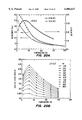
- FIGS. 14A-14B illustrate resistivity vs. temperature plots: (A) ⁇ BiCuSrCaO; and (B) ⁇ BiCuSrCaCuCaO and ⁇ BiCuCuSraCaO;
- FIG. 15 illustrates the masks used to generate the YBCO-BSCCO library.
- FIGS. 16A-16C illustrates resistivity vs. temperature plots: (A) BiCuSrCaO; (B) YBaCaO; and (C) YBa 2 Cu 3 O x ;
- FIG. 17 illustrates the masks used to generate the libraries of cobalt oxide (CoO) thin-film materials
- FIGS. 19A and 19B illustrate MR ratios of representative samples in L2 (19A) and L3 (19B) as a function of magnetic field
- the solid lines are guides to the eye;
- FIGS. 21A, 21B and 21C illustrate the X-ray diffraction patterns (indexed for cubic perovskite structure) for Ba, Sr and Ca doped bulk samples, respectively; the X-ray diffraction patterns indicate that the structure of this new class of cobalt oxides is cubic perovskite with some slight distortion; and
- FIG. 22 illustrates the magnetization of the bulk sample La 0 .58 Sr 0 .41 CoO.sub. ⁇ under 1T field as a function of temperature.
- the solid line is a guide to the eye.
- the inset in FIG. 22 illustrates the MR ratios of the sample at different temperatures as a function of magnetic field.
- Substrate A material having a rigid or semi-rigid surface.
- at least one surface of the substrate will be substantially flat, although in some embodiments it may be desirable to physically separate synthesis regions for different materials with, for example, dimples, wells, raised regions, etched trenches, or the like.
- the substrate itself contains wells, raised regions, etched trenches, etc. which form all or part of the synthesis regions.
- small beads or pellets may be provided on the surface within dimples or on other regions of the surface or, alternatively, the small beads or pellets may themselves be the substrate.
- a predefined region is a localized area on a substrate which is, was, or is intended to be used for formation of a selected material and is otherwise referred to herein in the alternative as "known” region, "reaction” region, a “selected” region, or simply a "region.”
- the predefined region may have any convenient shape, e.g., linear, circular, rectangular, elliptical, wedge-shaped, etc. Additionally, the predefined region, i.e., the reaction site, can be a bead or pellet which is coated with a reactant component(s) of interest.
- the bead or pellet can be identified with a tag, such as an etched binary bar code that can be used to indicate the history of the bead or pellet, i.e., to identify which components were deposited thereon.
- a predefined region and, therefore, the area upon which each distinct material is synthesized is smaller than about 25 cm 2 , preferably less than 10 cm 2 , more preferably less than 5 cm 2 , even more preferably less than 1 cm 2 , still more preferably less than 1 mm 2 , and even more preferably less than 0.5 mm 2 .
- the regions have an area less than about 10,000 ⁇ m 2 , preferably less than 1,000 ⁇ m 2 , more preferably less than 100 ⁇ m 2 , and even more preferably less than 10 ⁇ m 2 .
- Radiation Energy which may be selectively applied including energy having a wavelength between 10 -14 and 10 4 meters including, for example, electron beam radiation, gamma radiation, x-ray radiation, ultraviolet radiation, visible light, infrared radiation, microwave radiation and radio waves. "Irradiation” refers to the application of radiation to a surface.
- Component is used herein to refer to each of the individual chemical substances that act upon one another to produce a particular material and is otherwise referred to herein in the alternative as “reactant” or “reactant component.” That is to say, the components or, alternatively, reactants are the molecules that act upon one another to produce a new molecule(s), i.e., product(s); for example, in the reaction HCl+NaOH ⁇ NaCl+H 2 O, the HCl and the NaOH are the components or reactants.
- Material is used herein to refer to solid-state compounds, extended solids, extended solutions, clusters of molecules or atoms, crystals, etc.
- Covalent Network Solids Solids that consist of atoms held together in a large network of chains by covalent bonds. Such covalent network solids include, but are not limited to, diamond, silicon nitride, graphite, bunkmisterfullerene and organic polymers which cannot be synthesized in a stepwise fashion.
- Ionic Solids Solids which can be modeled as cations and anions held together by electrical attraction of opposite charge. Such ionic solids include, but are not restricted to, CaF 2 , CdCl 2 , ZnCl 2 , NaCl 2 , AgF, AgCl, AgBr and spinels (e.g., ZnAl 2 O 4 , MgAl 2 O 4 , FrCr 2 O 4 , etc.).
- Solids consisting of atoms or molecules held together by intermolecular forces.
- Molecular solids include, but are not limited to, extended solids, solid neon, organic compounds, synthetic or organic metals (e.g., tetrathiafulvalene-tetracyanoquinonedimethane (TTF-TCNQ)), liquid crystals (e.g., cyclic siloxanes) and protein crystals.
- TTF-TCNQ tetrathiafulvalene-tetracyanoquinonedimethane
- TTF-TCNQ tetrathiafulvalene-tetracyanoquinonedimethane
- liquid crystals e.g., cyclic siloxanes
- protein crystals e.g., cyclic siloxanes
- inorganic Materials Materials which do not contain carbon as a principal element.
- the oxides and sulphides of carbon and the metallic carbides are considered inorganic materials.
- examples of inorganic compounds which can be synthesized using the methods of the present invention include, but are not restricted to, the following:
- Intermetallic compounds constitute a unique class of metallic materials that form long-range ordered crystal structures below a critical temperature. Such materials form when atoms of two metals combine in certain proportions to form crystals with a different structure from that of either of the two metals (e.g., NiAl, CrBe 2 , CuZn, etc.).
- Metal Alloys A substance having metallic properties and which is composed of a mixture of two or more chemical elements of which at least one is a metal.
- Magnetic Alloys An alloy exhibiting ferromagnetism such as silicon iron, but also iron-nickel alloys, which may contain small amounts of any of a number of other elements (e.g., copper, aluminum, chromium, molybdenum, vanadium, etc.), and iron-cobalt alloys.
- Ceramics typically, a ceramic is a metal oxide, boride, carbide, nitride, or a mixture of such materials. Ceramics are inorganic, nonmetallic, nonmolecular solids, including both amorphous and crystalline materials. Ceramics are illustrative of materials that can be formed and screened for a particular property using the present invention.
- Such materials include, for example, alumina, zirconium, silicon carbide, aluminum nitride, silicon nitride, the YBa 2 Cu 3 O 7-8 superconductor, the La 2-x Sr x CuO 4 superconductors, the Bi 2 CaSr 2 Cu 2 O 8+x superconductors, the Ba 1-x K x BiO 3 superconductors, the ReBaCu superconductors, ferrite (BaFe 12 O 19 ), Zeolite A (Na 12 [(SiO 2 ) 12 (AlO 2 )]•27H 2 O), soft and permanent magnets, high dielectric constant materials (BaTiO 3 ), piezoelectric materials (e.g., lead zirconate titanate (PZT), NaNbO 3 , and NaTaO 3 ), electro-optic materials (e.g., lithium niobate (LiNbO 3 )), giant magnetoresistant materials (GMR), etc.
- a "giant magnetoresistant” material refers to a material having a change in resistance when exposed to a magnetic field that is greater than 5 percent relative to the resistance it had when no field was applied. That is to say, the absolute value of the percentage change in resistance is greater than 5 percent, i.e.,
- the change in resistance is determined by: ##EQU1## 10.
- Organic Materials Compounds, which generally consist of carbon and hydrogen, with or without oxygen, nitrogen or other elements, except those in which carbon does not play a critical role (e.g., carbonate salts).
- Non-biological, organic polymers Nonmetallic materials consisting of large macromolecules composed of many repeating units. Such materials can be either natural or synthetic, cross-linked or non-crosslinked, and they may be homopolymers, copolymers, or higher-ordered polymers (e.g., terpolymers, etc.).
- non-biological ⁇ -amino acids and nucleotides are excluded. More particularly, “non-biological, organic polymers” exclude those polymers which are synthesized by a linear, stepwise coupling of building blocks.
- Organometallic Materials A class of compounds of the type R-M, wherein carbon atoms are linked directly with metal atoms (e.g., lead tetraethyl (Pb(C 2 H 5 ) 4 ), sodium phenyl (C 6 H 5 •Na), zinc dimethyl (Zn(CH 3 ) 2 ), etc.).
- metal atoms e.g., lead tetraethyl (Pb(C 2 H 5 ) 4 ), sodium phenyl (C 6 H 5 •Na), zinc dimethyl (Zn(CH 3 ) 2 ), etc.
- Composite Materials Any combination of two materials differing in form or composition on a macroscale. The constituents of composite materials retain their identities, i.e., they do not dissolve or merge completely into one another although they act in concert. Such composite materials may be inorganic, organic or a combination thereof. Included with this definition are, for example, doped materials, dispersed metal catalysts and other heterogeneous solids.
- the present invention provides methods and apparatus for the preparation and use of a substrate having an array of materials in predefined regions thereon.
- the invention is described herein primarily with regard to the preparation of inorganic materials, but can readily be applied in the preparation of other materials.
- Materials which can be prepared in accordance with the methods of the present invention include, for example, covalent network solids, ionic solids and molecular solids.
- materials which can be prepared in accordance with the methods of the present invention include, but are not limited to, inorganic materials, intermetallic materials, metal alloys, ceramic materials, organic materials, organometallic materials, non-biological organic polymers, composite materials (e.g., inorganic composites, organic composites, or combinations thereof), or other materials which will be apparent to those of skill in the art upon review of this disclosure.
- the resulting substrate having an array of materials thereon will have a variety of uses.
- the substrate can be screened for materials having useful properties.
- the array of materials is preferably synthesized on a single substrate. By synthesizing the array of materials on a single substrate, screening the array for materials having useful properties is more easily carried out. Properties which can be screened for include, for example, electrical, thermal, mechanical, morphological, optical, magnetic, chemical, etc.
- properties which can be screened for include, for example, conductivity, superconductivity, resistivity, thermal conductivity, anisotropy, hardness, crystallinity, optical transparency, magnetoresistance, permeability, frequency doubling, photoemission, coercivity, dielectric strength, or other useful properties which will be apparent to those of skill in the art upon review of this disclosure.
- the synthesizing and screening of a diverse array of materials enables new compositions with new physical properties to be identified. Any material found to possess a useful property can be subsequently prepared on a large-scale. It will be apparent to those of skill in the art that once useful materials have been identified using the methods of the present invention, a variety of different methods can be used to prepare such useful materials on a large or bulk scale with essentially the same structure and properties.
- the array of materials is prepared by successively delivering components of materials to predefined regions on a substrate, and simultaneously reacting the components to form at least two materials.
- a first component of a first material is delivered to a first preferred region on a substrate, and a first component of a second material is delivered to a second preferred region on the same substrate.
- a second component of the first material is delivered to the first region on the substrate, and a second component of the second material is delivered to the second region on the substrate.
- Each component can be delivered in either a uniform or gradient fashion to produce either a single stoichiometry or, alternatively, a large number of stoichiometries within a single predefined region.
- reactants can be delivered as amorphous films, epitaxial films, or lattice or superlattice structures.
- the process is repeated, with additional components, to form a vast array of components at predefined, i.e., known, locations on the substrate. Thereafter, the components are simultaneously repeated to form at least two materials.
- the components can be sequentially or simultaneously delivered to predefined regions on the substrate using any of a number of different delivery techniques.
- the components after being delivered to predefined regions on the substrate, can be reacted using a number of different synthetic routes.
- the components can be reacted using, for example, solution based synthesis techniques, photochemical techniques, polymerization techniques, template directed synthesis techniques, epitaxial growth techniques, by the sol-gel process, by thermal, infrared or microwave heating, by calcination, sintering or annealing, by hydrothermal methods, by flux methods, by crystallization through vaporization of solvent, etc.
- solution based synthesis techniques photochemical techniques, polymerization techniques, template directed synthesis techniques, epitaxial growth techniques, by the sol-gel process, by thermal, infrared or microwave heating, by calcination, sintering or annealing, by hydrothermal methods, by flux methods, by crystallization through vaporization of solvent, etc.
- photochemical techniques photochemical techniques
- polymerization techniques template directed synthesis techniques
- epitaxial growth techniques by the sol-gel process
- the reaction conditions at different reaction regions can be controlled independently.
- reactant amounts, reactant solvents, reaction temperature, reaction times, the rates at which the reactions are quenched, deposition order of reactants, etc. can be varied from reaction region to reaction region on the substrate.
- the first component of the first material and the first component of the second material can be the same or different. If the first component of the first material is the same as the first component of the second materials, this component can be offered to the first and second regions on the substrate in ether the same or different amounts. This is true as well for the second component of the first material and the second component of the second material, etc.
- the second component of the first material and the second component of the second material can be the same or different and, if the same, this component can be offered to the first and second regions on the substrate in either the same or different amounts. Moreover, within a given predefined region on the substrate, the component can be delivered in either a uniform or gradient fashion. In addition, if the same components are delivered to the first and second regions on the substrate at identical concentrations, then the reaction conditions (e.g., reaction temperatures, reaction times, etc.) under which the reactions are carried out can be varied from reaction region to reaction region.
- the reaction conditions e.g., reaction temperatures, reaction times, etc.
- a method for forming at least two different arrays of materials by delivering substantially the same reactant components at substantially identical concentrations to reaction regions on both first and second substrates and, thereafter, subjecting the components on the first substrate to a first set of reaction conditions and the components on the second substrate to a second set of reaction conditions in a wide array of compositions.
- Reaction parameters which can be varied include, for example, reactant amounts, reactant solvents, reaction temperatures, reaction times, the pressures at which the reactions are carried out, the atmospheres in which the reactions are conducted, the rates at which the reactions are quenched, the order in which the reactants are deposited, etc.
- Other reaction parameters which can be varied will be apparent to those of skill in the art.
- the reactant components in the individual reaction regions must often be prevented from moving to adjacent reaction regions. Most simply, this can be ensured by leaving a sufficient amount of space between the reaction regions on the substrate so that the various components cannot interdiffuse between reaction regions. Moreover, this can be ensured by providing an appropriate barrier between the various reaction regions on the substrate.
- a mechanical device or physical structure defines the various reaction regions on the substrate.
- a wall or other physical barrier can be used to prevent the reactant components in the individual reaction regions from moving to adjacent reaction regions. This wall or physical barrier can be removed after the synthesis is carried out.
- a hydrophobic material for example, can be used to coat the region surrounding the individual reaction regions.
- Such materials prevent aqueous (and certain other polar) solutions from moving to adjacent reaction regions on the substrate.
- aqueous or nonpolar solvents when non-aqueous or nonpolar solvents are employed, different surface coatings will be required.
- appropriate materials e.g., substrate material, hydrophobic coatings, reactant solvents, etc.
- a small, precisely metered amount of each reactant component is delivered into each reaction region.
- This may be accomplished using a variety of delivery techniques, either alone or in combination with a variety of masking techniques.
- thin-film deposition techniques in combination with physical masking or photolithographic techniques can be used to deliver the various reactant components to selected regions on the substrate.
- sputtering systems, spraying techniques, laser ablation techniques, electron beam or thermal evaporation, ion implantation or doping techniques, chemical vapor deposition (CVD), as well as other techniques used in the fabrication of integrated circuits and epitaxially grown materials can be applied to deposit highly uniform layers of the various reactant components on selected regions on the substrate.
- a gradient of reactant components can be deposited within each predefined regions on the substrate or, alternatively, over all of the predefined regions on the substrate.
- Such thin-film deposition techniques are generally used in combination with masking techniques to ensure that the reactant components are being delivered only to the reaction regions of interest.
- the various reactant components can be deposited on the reaction regions of interest from a dispenser in the form of droplets or powder.
- Conventional micropipetting apparatuses can, for example, be adapted to dispense droplet volumes of 5 nanoliters or smaller from a capillary. Such droplets can fit within a reaction region having a diameter of 300 ⁇ m or less when a mask is employed.
- the dispenser can also be of the type employed in conventional ink-jet printers.
- ink-jet dispenser systems include, for example, the pulse pressure type dispenser system, the bubble jet type dispenser system and the slit jet type dispenser system. These ink-et dispenser systems are able to deliver droplet volumes as small as 5 picoliters.
- such dispenser systems can be manual or, alternatively, they can be automated using, for example, robotics techniques.
- the dispenser of the present invention can be aligned with respect to the appropriate reaction regions by a variety of conventional systems.
- Such systems which are widely used in the microelectronic device fabrication and testing arts, can deliver droplets of reactant components to individual reaction regions at rates of up to 5,000 drops per second.
- the translational (X-Y) accuracy of such systems is well within 1 ⁇ m.
- the position of the dispenser stage of such systems can be calibrated with respect to the position of the substrate by a variety of methods known in the art. For example, with only one or two reference points on the substrate surface, a “dead reckoning" method can be provided to locate each reaction region on the substrate.
- the reference marks in any such systems can be accurately identified by using capacitive, resistive or optical sensors.
- a "vision" system employing a camera can be employed.
- the dispenser can be aligned with respect to the reaction region of interest by a system analogous to that employed in magnetic and optical storage media fields.
- the reaction region in which the reactant component is to be deposited is identified by its track and sector location on the disk substrate.
- the dispenser is then moved to the appropriate track while the disk substrate rotates.
- a droplet of reactant solution is released.
- the reaction regions may be further defined by dimples in the substrate surface. This will be especially advantageous when a head or other sensing device must contact or glide along the substrate surface.
- the dimples can also act as identification marks directing the dispenser to the reaction region of interest.
- the methods of the present invention are used to prepare an array of diverse materials at known locations on a single substrate surface.
- any conceivable substrate can be employed in the invention.
- the substrate can be organic, inorganic, biological, nonbiological, or a combination of any of these, existing as particles, strands, precipitates, gels, sheets, tubing, spheres, containers, capillaries, pads, slices, films, plates, slides, etc.
- the substrate can have any convenient shape, such a disc, square, sphere, circle, etc.
- the substrate is preferably flat, but may take on a variety of alternative surface configurations. For example, the substrate may contain raised or depressed regions on which the synthesis of diverse materials takes place.
- the substrate and its surface preferably form a rigid support on which to carry out the reactions described herein.
- the substrate may be any of a wide variety of materials including, for example, polymers, plastics, pyrex, quartz, resins, silicon, silica or silica-based materials, carbon, metals, inorganic glasses, inorganic crystals, membranes, etc.
- Other substrate materials will be readily apparent to those of skill in the art upon review of this disclosure.
- Surfaces on the solid substrate can be composed of the same materials as the substrate or, alternatively, they can be different, i.e., the substrates can be coated with a different material.
- the substrate surface can contain thereon an adsorbent (for example, cellulose) to which the components of interest are delivered.
- adsorbent for example, cellulose
- a predefined region on the substrate and, therefore, the area upon which each distinct material is synthesized is smaller than about 25 cm 2 , preferably less than 10 cm 2 , more preferably less than 5 cm 2 , even more preferably 1 cm 2 , still more preferably less than 1 mm 2 , and still more preferably less than 0.5 mm 2 .
- the regions have an area less than about 10,000 ⁇ m 2 , preferably less than 1,000 ⁇ m 2 , more preferably less than 100 ⁇ m 2 , and even more preferably less than 10 ⁇ m 2 .
- a single substrate has at least 10 different materials and, more preferably, at least 100 different materials synthesized thereon. In even more preferred embodiments, a single substrate has more than 10 3 , 10 4 , 10 5 , 10 6 , or more materials synthesized thereon. In some embodiments, the delivery process is repeated to provide materials with as few as two components, although the process can be readily adapted to form materials having 3, 4, 5, 6, 7, 8 or more components therein.
- the density of regions per unit area will be great than 0.04 regions/cm 2 , more preferably greater than 0.1 regions/cm 2 , even more preferably greater than 1 region/cm 2 , even more preferably greater than 10 regions/cm 2 , and still more preferably greater than 100 regions/cm 2 .
- the density of regions per unit area will be greater than 1,000 regions/cm 2 , more preferably 10,000 regions/cm 2 , even more preferably greater than 100,000 regions/cm 2 , and still more preferably 10,000,000 regions/cm 2 .
- the substrate can be a series of small beads or pellets hereinafter "beads").
- the number of beads used will depend on the number of materials to be synthesized and can range anywhere from 2 to an infinite number of beads.
- each of the beads is uniformly coated with the reactant component(s) of interest and, thereafter, reacted. This is readily done, for example, by using a series of vessels each of which contains a solution of a particular reactant component. The beads are equally divided into groups corresponding to the number of components used to generate the array of materials. Each group of beads is then added to one of the vessels wherein a coating of one of the components in solution forms on the surface of each bead.
- each of the individual beads or pellets can be screened for materials having useful properties.
- an array of materials is to be generated based on Bi, Cu, Ca and Sr using a series of beads as the substrate, for example, four vessels containing aqueous solutions of Bi(NO 3 ) 3 , Cu(NO 3 ) 3 , Ca(NO 3 ) 3 and Sr(NO 3 ) 3 would be employed.
- a portion of the beads are added to the vessel containing the Bi(NO 3 ) 3 solution; a portion of the beads are added to the Cu(NO 3 ) 3 solution; a portion of the beads are added to the vessel containing the Ca(NO 3 ) solution; and, finally, a portion of the beads are added to the vessel containing the Sr(NO 3 ) 3 solution.
- the beads are removed from the vessel, dried, etched, pooled together into one group and, thereafter, subsequently divided and added to the vessels containing the foregoing reactant components of interest.
- the process is optionally repeated, with additional reactant components, to form a vast array of components on each of the beads.
- a number of variations can be made to this technique to generate a vast array of beads containing a vast array of components thereon.
- some of the beads can be coated with only two components, others with more than two components.
- some of the beads can be coated two or more times with the same component, whereas other beads are coated a single time with a given component.
- the substrate is preferably flat, but may take on a variety of alternative surface configurations. Regardless of the configuration of the substrate surface, it is imperative that the reactant components in the individual reaction regions be prevented from moving to adjacent reaction regions. Most simply, this can be ensured by leaving a sufficient amount of space between the regions on the substrate so that the various components cannot interdiffuse between reaction regions. Moreover, this can be ensured by providing an appropriate barrier between the various reaction regions on the substrate.
- a mechanical device or physical structure can be used to define the various regions on the substrate. For example, a wall or other physical barrier can be used to prevent the reactant components in the individual reaction regions from moving to adjacent reaction regions. Alternatively, a dimple or other recess can be used to prevent the reactant components in the individual reaction regions from moving to adjacent reaction regions.
- the dimples must be sufficiently small to allow close packing on the substrate.
- the dimples will be less than 1 mm in diameter, preferably less than 0.5 mm in diameter, more preferably less than 10,000 ⁇ m in diameter, even more preferably less than 100 ⁇ m in diameter, and still more preferably less than 25 ⁇ m in diameter.
- Dimples having these characteristics can be produced by a variety of techniques including laser, pressing, or etching techniques.
- a suitable dimpled substrate surface can, for example, be provided by pressing the substrate with an imprinted "master" such as those commonly used to prepare compact optical disks.
- an isotopic or anisotropic etching technique employing photolithography can be employed. In such techniques, a mask is used to define the reaction regions on the substrate. After the substrate is irradiated through the mask, selected regions of the photoresist are removed to define the arrangement of reaction regions on the substrate. The dimples may be cut into the substrate with standard plasma or wet etching techniques.
- suitable wet etch materials can include hydrogen fluoride, or other common wet etchants used in the field of semiconductor device fabrication.
- Suitable plasma etchants commonly used in the semiconductor device fabrication field can also be employed.
- plasma etchants include, for example, mixtures of halogen containing gases and inert gases.
- a plasma etch will produce dimples having a depth of less than 10 ⁇ m, although depths of up to 50 ⁇ m may be obtained under some conditions.
- a photochemically etchable glass known as "FOTOFORM” is available from Corning Glass Company (New York). Upon exposure to radiation through a mask, the glass becomes soluble in aqueous solutions. Thereafter, the exposed glass is simply washed with the appropriate solution to form the dimpled surface.
- well-defined dimples can be made having aspect ratios of 10 to 1 (depth to diameter) or greater, and depths of up to 0.1 inches. Dimple diameters can be made as small as 25 ⁇ m in a 250 ⁇ m thick glass layer.
- the dimpled surface can contain thereon an adsorbent (for example, cellulose) to which the components of interest are delivered.
- the liquid drop will form a bead (a phenomenon known as "lensing"). If, on the other hand, the sum of the liquid-air and liquid-solid tensions is less than the solid-air tension, the drop will not be confined to a given location, but will instead spread over the surface. Even if the surface tensions are such that the drop will not spread over the surface, the contact or wetting angle (i.e., the angle between the edge of the drop and the solid substrate) may be sufficiently small such that the drop will cover a relatively large area (possibly extending beyond the confines of a given reaction region).
- wetting angles can lead to formation of a thin (approximately 10 to 20 ⁇ ) "precursor film” which spreads away from the liquid bead.
- Larger wetting angles provide "taller" beads that take up less surface area on the substrate and do not form precursor films. Specifically, if the wetting angle is greater than about 90°, a precursor film will not form.
- Methods for controlling chemical compositions and, in turn, the local surface free energy of a substrate surface include a variety of techniques apparent to those in the art. Chemical vapor deposition techniques as well as other techniques applied in the fabrication of integrated circuits can be applied to deposit highly uniform layers on selected regions of the substrate surface. If, for example, an aqueous reactant solution is used, the area surface inside the reaction regions may be hydrophilic, while the surface surrounding the reaction regions may be hydrophobic. As such, the surface chemistry can be varied from position to position on the substrate to control the surface free energy and, in turn, the contact angle of the drops of reactant solution. In this manner, an array of reaction regions can be defined on the substrate surface.
- the reactant components in the individual reaction regions can be prevented from moving to adjacent reaction regions by leaving a sufficient amount of space between the regions on the substrate so that the various components cannot interdiffuse between reaction regions.
- a small, precisely metered amount of each reactant component is delivered to each reaction region. This may be accomplished using a variety of delivery techniques, either alone or in combination with a variety of physical masking or photolithographic techniques. Delivery techniques which are suitable for use in the methods of the present invention can generally be broken down into those involving the use of thin-film deposition techniques and those involving the use of dispensers.
- Thin-film deposition techniques in combination with physical masking techniques or photolithographic techniques can be used to deposit thin-films of the various reactants on predefined regions on the substrate.
- Such thin-film deposition techniques can generally be broken down into the following four categories: evaporative methods, glow discharge processes, gas-phase chemical processes, and liquid-phase chemical techniques. Included within these categories are, for example, sputtering techniques, spraying techniques, laser ablation techniques, electron beam or thermal evaporation techniques, ion implantation or doping techniques, chemical vapor deposition techniques, as well as other techniques used in the fabrication of integrated circuits. All of these techniques can be applied to deposit highly uniform layers, i.e., thin-films, of the various reactants on selected regions on the substrate.
- such thin-film deposition techniques can be used to generate uniform gradients at each reaction region on the substrate or, alternatively, over all of the reaction regions on the substrate.
- Thin-films of the various reactants can be deposited on the substrate using evaporative methods in combination with physical masking techniques.
- evaporative methods in thermal evaporation or vacuum evaporation methods, the following sequential steps take place: (1) a vapor is generated by boiling or subliming a target material; (2) the vapor is transported from the source to a substrate; and (3) the vapor is condensed to a solid film on the substrate surface.
- Evaporants, i.e., target materials which can be used in the evaporative methods cover an extraordinary range of chemical reactivities and vapor pressures and, thus, a wide vary of sources can be used to vaporize the target materials.
- Such sources include, for example, resistance-heated filaments, electron beams; crucible heated by conduction, radiation or rf-inductions; and arcs, exploding wires and lasers.
- thin-film deposition using evaporative methods is carried out using lasers, filaments, electron beams or ion beams as the source. Successive rounds of deposition, through different physical masks, using evaporative methods can be used to generate an array of reactants on a substrate for parallel synthesis.
- Molecular Beam Epitaxy is an evaporative method that can be used to grow epitaxial thin-films.
- the films are formed on single-crystal substrates by slowly evaporating the elemental or molecular constituents of the film from separate Knudsen effusion source cells (deep crucibles in furnaces with cooled shrouds) onto substrates held at temperatures appropriate for chemical reaction, epitaxy and re-evaporation of excess reactants.
- the Knudsen effusion source cells produce atomic or molecular beams of relatively small diameter which are directed at the heated substrate, usually silicon or gallium arsenide.
- Fast shutters are interposed between the source cells and the substrates. By controlling these shutters, one can grow superlattices with precisely controlled uniformity, lattice match, composition, dopant concentrations, thickness and interfaces down to the level of atomic layers.
- thin-films of the various reactants can be deposited on the substrate using glow-discharge processes in combination with physical masking techniques.
- the most basic and well known of these processes is sputtering, i.e., the ejection of surface atoms from an electrode surface by momentum transfer from bombarding ions to surface atoms.
- Sputtering or sputter-deposition is a term used by those of skill in the art to cover a variety of processes, all of which can be used in the methods of the present invention.
- One such process is RF/DC Glow Discharge Plasma Sputtering. In this process, a plasma of energized ions is created by applying a high RF or DC voltage between a cathode and an anode.
- Ion-Beam Sputtering is another example of a sputtering process which can be used to deposit thin-films of the various reactant components on a substrate. Ion-Beam Sputtering is similar to the foregoing process except the ions are supplied by an ion source and not a plasma. It will be apparent to one of skill in the art that other sputtering techniques (e.g., diode sputtering, reactive sputtering, etc.) and other glow-discharge processes can be used in the methods of the present invention to deposit thin-films on a substrate. Successive rounds of deposition, through different physical masks, using sputtering or other glow-discharge techniques can be used to generate an array of reactants on a substrate for parallel synthesis.
- sputtering techniques e.g., diode sputtering, reactive sputtering, etc.
- glow-discharge processes can be used in the methods of the present invention to deposit thin-films on a substrate
- FIG. 1 An example of an eight RF magnetron sputtering gun system which can be employed in the methods of the present invention is illustrated in FIG. 1.
- This system comprises eight RF magnetron sputtering guns 110, each of which contains a reactant component of interest.
- the eight RF magnetron sputtering guns are located about 2 to about 5 inches above a disk 112 containing thereon eight masking patterns 114 as well as eight film-thickness monitors 116.
- the eight RF magnetron sputtering guns as well as the disk are fixed.
- the substrate 118 is coupled to a substrate manipulator 120 which is capable of linear and rotational motion and which engages the substrate with the particular mask of interest so that the substrate is in contact with the mask when the sputtering begins.
- a substrate manipulator 120 which is capable of linear and rotational motion and which engages the substrate with the particular mask of interest so that the substrate is in contact with the mask when the sputtering begins.
- Combinations of the eight components are generated on the substrate by the sequential deposition of each component through its respective mask. This entire system is used in vacuo.
- CVD Chemical Vapor Deposition
- Photo-Enhanced CVD based on activation of the reactants in the gas or vapor phase by electromagnetic radiation, usually short-wave ultraviolet radiation
- Plasma-Assisted CVD based on activation of the reactants in the gas or vapor phase using a plasma
- Successive rounds of deposition, through different physical masks, using CVD technique can be used to generate an array of reactants on a substrate for parallel synthesis.
- thin-films of the various reactants can be deposited on a substrate using a number of different mechanical techniques in combination with physical masking techniques.
- mechanical techniques include, for example, spraying, spinning, dipping, draining, flow coating, roller coating, pressure-curtain coating, brushing, etc.
- spray-on and spin-on techniques are particularly useful.
- Sprayers which can be used to deposit thin-films include, for example, ultrasonic nozzle sprayers, air atomizing nozzle sprayers and atomizing nozzle sprayer.
- ultrasonic sprayers disc-shaped ceramic piezoelecric transducers covert electrical energy into mechanical energy.
- the transducers receive electrical input in the form of a high-frequency signal from a power supply that acts as a combination oscillator/amplifier.
- a power supply that acts as a combination oscillator/amplifier.
- the nozzles intermix air and liquid streams to produce a completely atomized spray.
- the nozzles use the energy from a pressurized liquid to atomize the liquid and, in turn, produce a spray.
- Successive rounds of deposition, through different physical masks, using mechanical techniques, such as spraying, can be used to generate an array of reactants on a substrate for parallel synthesis.
- photolithographic techniques of the type known in the semiconductor industry can be used.
- photolithographic techniques of the type known in the semiconductor industry can be used.
- Sze Sze
- VLSI Technology McGraw-Hill (1983)
- Mead, et al. Introduction to VLSI Systems, Addison-Wesley (1980)
- a number of different photolithographic techniques known to those of skill in the art can be used.
- a photoresist is deposited on the substrate surface; the photoresist is selectively exposed, i.e., photolyzed; the photolyzed or exposed photoresist is removed; a reactant is deposited on the exposed region(s) on the substrate; and the remaining unphotolyzed photoresist is removed.
- a negative photoresist the photoresist is deposited on the substrate surface; the photoresist is selectively exposed, i.e., photolyzed; the unphotolyzed photoresist is removed; a reactant is deposited on the exposed region(s) on the substrate; and the remaining photoresist is removed.
- a reactant is deposited on the substrate using, for example, spin-on or spin-coating techniques; a photoresist is deposited on top of the reactant; the photoresist is selectively exposed, i.e., photolyzed; the photoresist is removed from the exposed region(s); the exposed region(s) are etched to remove the reactant from that region(s); and the remaining unphotolyzed photoresist is removed.
- a negative photoresist can be used in place of the positive photoresist.
- photolithographic techniques can be repeated to produce an array of reactants on a substrate for parallel synthesis.
- FIG. 2 and FIG. 3 illustrate the use of the physical masking techniques which can be used in conjunctions with the aforementioned thin-film deposition techniques. More particularly, FIG. 2 illustrates one embodiment of the invention disclosed herein in which a substrate 2 is shown in cross-section.
- the mask 8 can be any of a wide variety of different materials including, for example, polymers, plastics, resins, silicon, metals, inorganic glasses, etc. Other suitable mask materials will be readily apparent to those of skill in the art.
- the mask is brought into close proximity with, imaged on, or brought directly into contact with the substrate surface as shown in FIG. 2. "Openings" in the mask correspond to regions on the substrate where it is desired to deliver a reactant.
- the openings in the mask can take on a variety of different sizes and shapes.
- the openings are circular, rectangular or square. Alternatively, however, they can be linear such that the components are delivered in a linear fashion from one end of the substrate to the other. This "linear" arrangement facilitates screening or detection in certain instances, such as when thermoelectric materials are being discovered and optimized.
- Conventional binary masking techniques in which one-half of the mask is exposed at a given time are illustrated hereinbelow. It will be readily apparent to those of skill in the art, however, that masking techniques other than conventional binary masking techniques can be used in the methods of the present invention.
- the substrate 2 is provided with regions 22, 24, 26, 28, 30, 32, 34, 36, 38, 40, 42, 44, 46, 48, 50 and 52.
- Regions 38, 40, 42, 44, 46, 48, 50 and 52 are masked, as shown in FIG. 3B, and component A is delivered to the exposed regions in the form of a thin-film using, for example, spraying or sputtering techniques, with the resulting structure shown in FIG. 3C.
- the mask is repositioned so that regions 26, 28, 34, 36, 42, 44, 50 and 52 are masked, as shown in FIG. 3D, and component B is delivered to the exposed regions in the form of a thin-film, with the resulting structure shown in FIG. 3E.
- a second mask can be used and, in fact, multiple masks are frequently required to generate the desired array of reactants. If multiple masking steps are used, alignment of the masks may be performed using conventional alignment techniques in which alignment marks (not shown) are used to accurately overly successive masks with previous patterning steps, or more sophisticated techniques can be used. Moreover, it may be desirable to provide separation between exposed areas to account for alignment tolerances and to ensure separation of reaction sites so as to prevent cross-contamination. In addition, it will be understood by those of skill in the art that the delivery techniques used to deliver the various reactants to the regions of interest can be varied from reactant to reactant, but, in most instances, it will be most practical to use the same deposition technique for each of the reactants.
- regions 30, 32, 34, 36, 46, 48, 50 and 52 are masked, as shown in FIG. 3F, using a mask different from that used in the delivery of components A and B.
- Component C is delivered to the exposed regions in the form of a thin-film, with the resulting structure shown in FIG. 3G.
- regions 24, 28, 32, 36, 40, 44, 48 and 52 are masked, as shown in FIG. 3H, and component D is delivered to the exposed regions in the form of a thin-film, with the resulting structure shown in FIG. 3I.
- FIG. 4 illustrates a masking technique which can be employed to generate an array of materials, each consisting of a combination of three different components, formed from a base group of four different components.
- a separate mask is employed for each of the different components.
- four different masks are employed.
- the substrate 2 is provided with regions 54, 56, 58 and 60. Region 56 is masked, as shown in FIG.
- component A is delivered to the exposed regions in the form of a thin-film using, for example, spraying or sputtering techniques, with the resulting structure shown in FIG. 4C.
- a second mask is employed to mask region 54, as shown in FIG. 4D, and component B is delivered to the exposed regions in the form of a thin-film, with the resulting structure shown in FIG. 4E.
- region 58 is masked using a third mask, as shown in FIG. 4F, and component C is delivered to the exposed regions in the form of a thin-film, with the resulting structure shown in FIG. 4G.
- a fourth mask is employed to mask region 60, as shown in FIG.
- component D is delivered to the exposed regions in the form of a thin-film, with the resulting structure shown in FIG. 4I.
- components of interest Once the components of interest have been delivered to appropriate predefined regions on the substrate, they are simultaneously reacted using any of a number of different synthetic routes to form an array of four different materials.
- FIG. 5 illustrates another masking technique which can be employed to generate an array of materials, each consisting of a combination of three different components, formed from a base group of six different components.
- the substrate 2 is provided with regions 62, 64, 66, 68, 70, 72, 74, 76, 78, 80, 82, 84, 86, 88, 90, 92, 94, 96, 98 and 100.
- Regions 64, 68, 72, 76, 80, 84, 88, 92, 96 and 100 are masked, as shown in FIG.
- component A is delivered to the exposed regions in the form of a thin-film using, for example, spraying or sputtering techniques, with the resulting structure shown in FIG. 5C.
- a second mask is employed to mask regions 62, 66, 72, 74, 80, 82, 88, 90, 96 and 98, as shown in FIG. 5D, and component B is delivered to the exposed regions in the form of a thin-film, with the resulting structure shown in FIG. 5E.
- regions 64, 66, 70, 74, 78, 82, 86, 92, 96, and 100 are masked using a third mask, as shown in FIG.
- a fourth mask is employed to mask regions 64, 66, 70, 76, 78, 84, 88, 90, 94 and 98, as shown in FIG. 5H, and component D is delivered to the exposed regions in the form of a thin-film, with the resulting structure shown in FIG. 5I.
- regions 62, 68, 70, 74, 80, 84, 86, 90, 94 and 100 are masked with a fifth mask, as shown in FIG. 5J, and component E is delivered to the exposed regions in the form of a thin-film, with the resulting structure shown in FIG. 5K.
- a sixth mask is employed to mask regions 62, 68, 72, 76, 78, 82, 86, 92, 94 and 98, as shown in FIG. 5L, and component F is delivered to the exposed regions in the form of a thin-film, with the resulting structure shown in FIG. 5M.
- an additional reactant component can be delivered to the predefined regions on the substrate in a gradient of stoichiometries.
- a seventh component can be delivered in a gradient fashion across the entire substrate or across portions of the substrate.
- the seventh component can, for example, be deposited through an appropriate mask from left to right as a gradient layer ranging from about 100 ⁇ to 1,000 ⁇ in thickness.
- the reactant components can be simultaneously reacted using any of a number of different synthetic routes to form an array of different materials.
- dispensers can be utilized to generate diverse combinations of reactant components in the form of droplets or powder on a single substrate.
- commercially available micropipetting apparatus can be adapted to dispense droplet volumes of 5 nanoliters or smaller from a capillary. Such droplets can fit within a reaction region having a diameter of 300 ⁇ m or less when a non-wetting mask is employed.
- the micropipette is accurately and precisely positioned above the reaction, as described below, before the reactant solution is deposited.
- the present invention employs a solution depositing apparatus that resembles devices commonly employed in the ink-jet printing field.
- ink-jet dispensers include, for example, the pulse pressure type, the bubble jet type and the slit jet type.
- the printing ink is jetted from a nozzle according to a change in pressure applied by a piezoelectric device.
- ink-jet dispenser of the bubble jet type bubbles are generated with heat generated with a resistance device embedded in a nozzle, and printing ink is jetted by using the force due to the expansion of a bubble.
- an ink-jet dispenser of the slit jet type printing ink is filled within a slit-like orifice wherein recording electrodes are aligned in correspondence to pixels, and a DC voltage pulse is applied between a recording electrode and a counter electrode arranged behind a recording paper.
- the printing ink around the top of the record electrode is charged electrically so that the ink is ejected towards the recording paper with an electrostatic force to record a dot on the paper.
- Such ink-jet printers can be used with minor modification by simply substituting a reactant containing solution or reactant containing powder for the ink.
- a reactant containing solution or reactant containing powder for the ink.
- Wong, et al. European Patent Application 260 965, incorporated herein by reference for all purposes, describes the use of a pulse pressure type ink-jet printer to apply an antibody to a solid matrix.
- a solution containing the antibody is forced through a small bore nozzle that is vibrating in a manner that fragments the solution into discrete droplets.
- the droplets are subsequently charged by passing through an electric field and then deflected onto the matrix material.
- a conventional ink drop printer of the pulse pressure type includes a reservoir in which ink is held under pressure.
- the ink reservoir feeds a pipe which is connected to a nozzle.
- An electromechanical transducer is employed to vibrate the nozzle at some suitably high frequency.
- the actual structure of the nozzle may have a number of different constructions, including a drawn glass tube which is vibrated by an external transducer, or a metal tube vibrated by an external transducer (e.g., a piezoelectric crystal), or a magnetostrictive metal tube which is magnetostrictively vibrated.
- the ink accordingly is ejected from the nozzle in a stream which shortly thereafter breaks into individual drops.
- An electrode may be present near the nozzle to impart a charge to the droplets.
- FIG. 6 A schematic drawing of an ink drop dispenser of the pulse pressure type (such as is described in U.S. Pat. Nos. 3,281,860 and 4,121,222, which are incorporated by reference herein for all purposes) which may be employed in the present invention is shown in FIG. 6.
- This apparatus comprises a reservoir 210 which contains a solution under pressure.
- Tubing 212 is connected to the reservoir 210 and terminates in a metal nozzle 242.
- Nozzle 242 is disposed within a hole provided in piezoelectric crystal 240. The end of the metal tube and of the piezoelectric crystal are made to coincide.
- the tubing and the piezoelectric crystal are soldered together to form a permanent waterproof attachment.
- a washer 244 which is termed an orifice washer.
- This washer has an opening 246 drilled therethrough through which the solution is emitted under pressure.
- a source of oscillations 218 is connected between the outside of the metal tubing 242 and the outside of the piezoelectric crystal 240.
- the construction is such that hermetic sealing can be employed which protects against electrochemical and atmospheric attack of the components.
- the piezoelectric crystal 240 is vibrated substantially at the frequency of the source of oscillations causing the tubing and nozzle to vibrate whereby the solution stream breaks down into droplets 246.
- a signal source 224 which is synchronized by the source of oscillations is connected between the nozzle and the charging cylinder 226.
- the charged drops after passing through the charging cylinder, pass into an electric field which is established between two plates respectively 230 and 232 which are connected to a field potential source 234.
- the drops are deflected from their center line path between the plates in accordance with the charge which they carry.
- an optionally moving writing medium 236 a deposition pattern occurs on the writing medium representative of the information in the signals.
- ink-jet printers of the pulse pressure type has been described in greater detail herein for purposes of illustration, it will be readily apparent to those of skill in the art that ink-jet printers of the bubble jet type and the slit jet type can also be used, with only minor modifications, to deliver reactant components to predefined regions on the substrate.
- ink-jet printers having multiple nozzles are used to deliver multiple reactant components to a single predefined region on the substrate or, alternatively, to multiple predefined regions on the substrate.
- improvements can be used in the methods of the present invention.
- the reactant solutions can be delivered from a reservoir to the substrate by an electrophoretic pump.
- a thin capillary connects a reservoir of the reactant with the nozzle of the dispenser.
- electrodes are present to provide a potential difference.
- the speed at which a chemical species travels in a potential gradient of an electrophoretic medium is governed by a variety of physical properties, including the charge density, size, and shape of the species being transported, as well as the physical and chemical properties of the transport medium itself. Under the proper conditions of potential gradient, capillary dimensions, and transport medium rheology, a hydrodynamic flow will be set up within the capillary.
- bulk fluid containing the reactant of interest can be pumped from a reservoir to the substrate.
- the reactant solution can be precisely delivered to predefined reaction regions on the substrate.
- the reactants can be delivered to predefined regions on the substrate either sequentially or simultaneously.
- the reactants are simultaneously delivered to either a single predefined region on the substrate or, alternatively, to multiple predefined regions on the substrate.
- an ink-jet dispenser having two nozzles
- two different reactants can be simultaneously delivered to a single predefined region on the substrate.
- a reactant can be simultaneously delivered to two different predefined regions on the substrate. In this instance, the same reactant or, alternatively, two different reactants can be delivered. If the same reactant is delivered to both of the predefined regions, it can be delivered in either the same or different amounts.
- an ink-jet dispenser having eight nozzles, for example, eight different reactants can be simultaneously delivered to a single predefined region on the substrate or, alternatively, eight reactants (either the same or different) can be simultaneously delivered to eight different predefined regions on the substrate.
- a frame of reference common to the delivery instrument and the substrate is required.
- the reference coordinates of the instrument must be accurately mapped onto the reference coordinates of the substrate.
- only two reference points on the substrate are required to completely map the array of reaction regions.
- the dispenser instrument locates these reference points and then adjust its internal reference coordinates to provide the necessary mapping. After this, the dispenser can move a particular distance in a particular direction and be positioned directly over a known region. Of course, the dispenser instrument must provide precisely repeatable movements. Further, the individual regions of the array must not move with respect to the reference marks on the substrate after the reference marks have been formed. Unfortunately, pressing or other mechanical operations commonly encountered during fabrication and use of a substrate may warp the substrate such that the correspondence between the reference marks and the reaction regions is altered.
- a substrate containing both "global” and “local” reference marks is preferably employed.
- only two global reference marks are conveniently located on the substrate to define the initial frame of reference.
- the dispenser instrument has an approximate map of the substrate and the predefined regions therein.
- the substrate is further subdivided into local frames of reference.
- the dispenser is positioned within one of the local frames of reference.
- the dispensing instrument looks for local reference marks to define further a local frame of reference. From these, the dispenser moves exactly to the reaction region where the reactant is to be deposited. In this manner, the effects of warpage or other deformation can be minimized.
- the number of local reference marks is determined by the amount of deformation expected in the substrate. If the substrate is sufficiently rigid so that little or no deformation will occur, very few local reference marks are required. If substantial deformation is expected, however, more local reference marks are required.
- the micropipette or other dispenser is translated from one reaction region to another reaction region on the substrate by a correct distance in the correct direction (this is the "dead reckoning" navigational technique).
- the dispenser can move from region to region, dispensing correctly metered amounts of reactants.
- a vision or blind system can be employed.
- a camera is rigidly mounted to the dispenser nozzle.
- the dispenser is known to be a fixed distance and direction away from the point, and a frame of reference is established.
- Blind systems locate the reference point(s) by capacitive, resistive, or optical techniques, for example.
- a laser beam is transmitted through or reflected from the substrate.
- a change in light intensity is detected by a sensor.
- Capacitive and resistive techniques are similarly applied.
- a sensor registers a change in capacitance or resistivity when a reference point is encountered.
- the spacing between the individual regions will vary in accordance with the size of the regions used. For example, if a 1 mm 2 region is used, the spacing between the individual regions will preferably be on the order of 1 mm or less. If, for example, a 10 ⁇ m 2 region is used, the spacing between the individual regions will preferably be on the order of 10 ⁇ m or less. Further, the angular relation between the cells is preferably consistent, to within 0.1 degrees. Of course, the photolithographic or other process used to define the arrangement of cells will accurately define the angle and spacing. However, in subsequent processes (e.g., pressing processes), the angle can be distorted. Thus, in some embodiments, it may be necessary to employ "local" reference points throughout the array.
- Translational mechanisms capable of moving with the desired precision are preferably equipped with position feedback mechanisms (i.e., encoders) of the type used in devices for semiconductor device manufacturing and testing. Such mechanisms will preferably be closed loop systems with insignificant backlash and hysteresis.
- the translation mechanism will have a high resolution, i.e., greater than five motor ticks per encoder count.
- the electro-mechanical mechanism will preferably have a high repeatability relative to the region diameter travel distance (preferably, ⁇ 1-5 ⁇ m).
- the dispenser nozzle To deposit a drop of reactant solution on the substrate accurately, the dispenser nozzle must be placed a correct distance above the surface.
- the dispenser tip preferably should be located about 0.1 cm to about 6 cm above the substrate surface when the drop is released. The degree of control necessary to achieve such accuracy can be attained with a repeatable high-resolution translation mechanism of the type described above.
- the height above the substrate is determined by moving the dispenser toward the substrate in small increments, until the dispenser tip touches the substrate. At this point, the dispenser is moved away from the surface a fixed number of increments which corresponds to a specific distance. From there, the drop is released to the cell below.
- the increments in which the dispenser moves will vary in accordance with the size of the regions used.
- the dispenser nozzle is encircled by a sheath that rigidly extends a fixed distance beyond the dispenser tip. Preferably, this distance corresponds to the distance at which the solution drop will fall when delivered to the selected reaction region.
- the sheath contacts the substrate surface, the movement of the dispenser is halted and the drop is released. It is not necessary in this embodiment to move the dispenser back, away from the substrate, after contact is made.
- the point of contact with the sure can be determined by a variety of techniques such as by monitoring the capacitance or resistance between the tip of the dispenser (or sheath) and the substrate below. A rapid change in either of these properties is observed upon contact with the surface.
- the dispenser delivery system has been described only in teams of translational movements. However, other systems may also be employed.
- the dispenser is aligned with respect to the region of interest by a system analogous to that employed in magnetic and optical storage media fields. For example, the region in which reactant is to be deposited is identified by a track and sector location on a disk substrate. The dispenser is then moved to the appropriate track while the disk substrate rotates. When the appropriate cell is positioned below the dispenser (as referenced by the appropriate sector on the track), a droplet of reactant solution is released.
- Control of the droplet size may be accomplished by various techniques known to those of skill in the art.
- a conventional micropipetting instrument is adapted to dispense droplets of five nanoliters or smaller from a capillary. Such droplets fit within regions having diameters of 300 ⁇ m or less when a non-wetting mask is employed.
- Pellets can be formed, for example, from the compound or component of interest and one or more kinds of inert binding material.
- the composition of such binders and methods for the preparation of such "pellets” will be apparent to those of skill in the art.
- Such "mini-pellets” will be compatible with a wide variety of test substances, stable for long periods of time and suitable for easy withdrawal from the storage vessel and dispensing.
- the components can be simultaneously reacted using a number of different synthetic routes.
- the components can be reacted using, for example, solution based synthesis techniques, photochemical techniques, polymerization techniques, template directed synthesis techniques, epitaxial growth techniques, or by the sol-gel process, by thermal, infrared or microwave heating, by calcination, sintering or annealing, by hydrothermal methods, by flux methods, by crystallization through vaporization of solvent, etc.
- solution based synthesis techniques for example, solution based synthesis techniques, photochemical techniques, polymerization techniques, template directed synthesis techniques, epitaxial growth techniques, or by the sol-gel process, by thermal, infrared or microwave heating, by calcination, sintering or annealing, by hydrothermal methods, by flux methods, by crystallization through vaporization of solvent, etc.
- Other useful synthesis techniques will be apparent to those of skill in the art upon review of this disclosure.
- the most appropriate synthetic route will depend on the class of materials to be synth
- the reactant components can be mixed prior to being reacted using, for example, ultrasonic techniques, mechanical techniques, etc.
- Such techniques can be applied directly to a given predefined region on the substrate or, alternatively, to all of the predefined regions on the substrate in a simultaneous fashion (e.g., the substrate can be mechanically moved in a manner such that the components are effectively mixed).
- reaction rates can be increased at lower temperatures by drastically shortening the distance required for diffusion of the reactants and by increasing the surface to volume ratio. This can be achieved by depositing the reactants on the substrate in the form of very thin-films or, alternatively, by using solution based synthesis techniques wherein the reactants are delivered to the substrate in the form of a solution.
- a molten salt can be employed to dissolve the reactant components. This technique is generally referred to as the flux method.
- a hydrothermal method water or other polar solvent containing a soluble inorganic salt is employed to dissolve the reactant components.
- the hydrothermal method is usually carried out under pressure and at a temperature ranging from about 100° C. to about 400° C.
- the array of reactant components can be pressurized or depressurized under an inert atmosphere, oxygen or other gas.
- various regions on the substrate can be exposed to different heat histories using, for example, laser thermolysis, wherein bursts of energy of a predetermined duration and intensity are delivered to target regions on the substrate.
- the predefined regions on a substrate can be subjected to different reaction temperatures by independently heating the predefined regions using a thin-film resistive element.
- a resistive element such as tungsten
- the resistive element is deposited, for example, in strips along the rows or columns of predefined regions. Each strip is connected to an electrical lead which is attached to a power supply.
- the temperature of the predefined regions can be regulated by varying the power input to a given strip. In general, any conductive material having a melting point higher than the temperature at which the reaction is to be carried out can be used as the resistive element.
- Suitable materials include, but are not limited to, metals, alloys, and ceramics. Examples of such materials include, but are not limited to, indium doped tin oxide (ITO), tungsten, molybdenum, tantalum, platinum, copper-nickel alloys, platinum and rhodium alloys, aluminum-nickel alloys, etc.
- ITO indium doped tin oxide
- tungsten tungsten
- molybdenum molybdenum
- tantalum platinum
- platinum copper-nickel alloys
- platinum and rhodium alloys aluminum-nickel alloys, etc.
- the resistive element it may be necessary to coat the resistive element with a protective coating so as to prevent interdiffusion between the resistive element and the array of components.
- the protective coating is applied in the form of a thin-film material using the previously described thin-film deposition techniques.
- the protective coating is made from a material which effectively conducts heat and which is inert at the temperature at which the reaction is to be carried out. Examples of suitable materials include, but are not limited to, MgO, SrTiO 3 , BaTiO 3 , Al 2 O 3 and other semiconductor and ceramic materials which are good conductors and inert.
- FIG. 7 An example of this approach is illustrated in FIG. 7.
- a library of compounds was generated subsequent to the deposition of thin-film resistive strips.
- a resistive element occupies an entire column of predefined regions on the substrate. It will be readily apparent to those of skill in the art, however, that the resistive element can be deposited in any pattern and, thus, deposition strategies can be designed so that the resistive element covers different predefined regions on the substrate.
- the array of components can be processed between the various delivery steps.
- component A can be delivered to a first region on a substrate and, thereafter, exposed to oxygen at an elevated temperature, for example.
- component B can be delivered to the first region on the substrate and, thereafter, components A and B can be reacted under a set of reaction conditions.
- Other manipulations and processing steps which can be carried out between the various delivery steps will be apparent to those of skill in the art upon reading this disclosure.
- the following materials can be prepared: covalent network solids, ionic solids and molecular solids. More particularly, the methods of the present invention can be used to prepare, for example, inorganic materials, intermetallic materials, metal alloys, ceramic materials, organic materials, organometallic materials, non-biological organic polymers, composite materials (e.g., inorganic composites, organic composites, or combinations thereof), etc. Ceramic can be prepared, for instance, by delivering reactant components to predefined regions on the substrate using, for example, solution based delivery techniques. Once the reactant components of interest have been delivered to the substrate, the substrate is heated to the boiling point of the solvent to evaporate off the solvent.
- the solvent can be removed by delivering the reactant components to a heated substrate.
- the substrate is then oxidized to remove unwanted components (e.g., carbon, nitrogen, etc.) from the array.
- the substrate is then flash heated at a temperature of about 800° C. to about 875° C. for about two minutes. Thereafter, the reaction is rapidly quenched and the array is scanned for materials having a particular property, such as luminescence, superconductivity, dielectric strength, etc.
- Magnetic materials can be prepared using a similar process except that in the case of magnetic materials, the components are delivered to the substrate and simultaneously reacted thereon in the presence of a magnetic field.
- an array of zeolites i.e., hydrated silicates of aluminum and either sodium, calcium or both, can be prepared using the methods of the present invention.
- the reactant components are delivered to predefined regions on a substrate in the form of a slurry.
- a low temperature e.g., 60° C. to about 70° C.
- organic polymers can be prepared by delivering a monomer (or monomers) of interest to predefined regions on the substrate usually in the form of a solution.
- an initiator is added to each region on the substrate. The polymerization reaction is allowed to proceed until the initiator is used up, or until the reaction is terminated in some other manner.
- the solvent can be removed by, for example, evaporation in vacuo.
- the array of materials can be screened in parallel for materials having useful properties. Either the entire array or, alternatively, a section thereof (e.g., a row of predefined regions) can be screened in parallel for materials having useful properties. Scanning detection systems are preferably utilized to screen an array of materials wherein the density of regions per unit area will be greater than 0.04 regions/cm 2 , more preferably greater than 0.1 regions/cm 2 , even more preferably greater than 1 region/cm 2 , even more preferably greater than 10 regions/cm 2 , and still more preferably greater than 100 regions/cm 2 .
- scanning detection systems are preferably utilized to screen an array of materials wherein the density of regions per unit area will be greater than 1,000 regions/cm 2 , more preferably 10,000 regions/cm 2 , even more preferably greater than 100,000 regions/cm 2 , and still more preferably 10,000,000 regions/cm 2 .
- the array of materials is synthesized on a single substrate.
- screening the array for materials having useful properties is more easily carried out.
- Properties which can be screened for include, for example, electrical, thermal mechanical, morphological, optical, magnetic, chemical, etc. More particularly, useful properties which can be screened for are set forth in Table I, infra. Any material found to possess a useful property can subsequently be prepared on a large-scale.
- Scanning systems which can be used to screen for the properties set forth in Table I include, but are not limited to, the following: scanning Raman spectroscopy; scanning NMR spectroscopy; scanning probe spectroscopy including, for example, surface potentialometry, tunnelling current, atomic force, acoustic microscopy, shearing-stress microscopy, ultra fast photo excitation, electrostatic force microscope, tunneling induced photo emission microscope, magnetic force microscope, microwave field-induced surface harmonic generation microscope, nonlinear alternating-current tunneling microscopy, near-field scanning optical microscopy, inelastic electron tunneling spectrometer, etc.; optical microscopy in different wavelengths; scanning optical ellipsometry (for measuring dielectric constant and multilayer film thickness); scanning Eddy-current microscope; electron (diffraction) microscope, etc.
- one of the following devices can be used: a Scanning RF Susceptibility Probe, a Scanning RF/Microwave Split-Ring Resonator Detector, or a Scanning Superconductors Quantum Interference Device (SQUID) Detection System.
- a nanoindentor diamond tip
- a Scanning RF/Microwave Split-Ring Resonator Detector or a SQUID Detection System can be used.
- crystallinity infrared or Raman spectroscopy can be used.
- a Scanning RF Susceptibility Probe a Scanning RF/Microwave Split-Ring Resonator Detector, a SQUID Detection System or a Hall probe can be used.
- a photodetector or a charged-coupled device camera can be used.
- Other scanning systems known to those of skill in the art can also be used.
- the arrays of the present invention can be screened sequentially or, alternatively, they can be screened in parallel using a scanning system.
- the array of materials can be sequentially screened for superconductivity using, for example, magnetic decoration (Bitter pattern) and electron holography.
- the array of materials can be scanned for superconductivity using, for example, a Hall-probe, magnetic force microscopy, SQUID microscopy, a AC susceptibility microscope, a microwave absorption microscope, an Eddy current microscope, etc.
- a scanning detection system is employed.
- the substrate having an array of materials thereon is fixed and the detector has X-Y motion.
- the substrate is placed inside a sealed chamber, close to the detector.
- the detector e.g., an RF Resonator, a SQUID detector, etc.
- the position of the detector is controlled using stepping motors (or servomotors) connected to a computer-controlled positioner.
- the temperature of the detector and the substrate can be lowered via helium exchange gas by liquid helium reservoir located around the chamber.
- This scanning system can be operated at temperatures ranging from 600° K. down to 4.2° K. (when immersed in liquid helium).
- the detector is fixed and the substrate having an array of materials thereon has R- ⁇ motion.
- the substrate is placed on a rotating stage (e.g., a spur gear) driven by a gear rack which is coupled to a micrometer and a stepping motor.
- This rotating stage is located on a cryogenic sliding table which is driven by a separate micrometer and stepping motor system.
- This system is capable of scanning an area having a 1 inch radius with a 1 ⁇ m spatial resolution. The scanning and probing are controlled through the use of a computer.
- the temperature of the detector and the substrate can be lowered via helium exchange gas using a liquid helium reservoir located around the chamber. This scanning system can be operated at temperatures ranging from 600° K. down to 4.2° K. (when immersed in liquid helium).
- a Scanning RF Susceptibility Detection System can, for example, be used to detect the superconductivity of a large array of materials (see, e.g., FIG. 8).
- a micro (about 1 ⁇ 1 mm 2 ) spiral coil can be fabricated to probe the conductivity of a sample adjacent to the coil.
- the signals are picked up by a phase-sensitive detection electronic circuit.
- the data is analyzed by a computer to obtain a correlation between the properties and stoichiometry of a given sample. If desired, analytical results can be fed back to the delivery system so that the system can "zoom in” on the most promising stoichiometry in the next synthesis cycle.
- a superconducting microcircuit implementation of a parallel LC resonance circuit can be used to scan the array of materials for those that are superconducting.
- a parallel LC circuit is simply an inductor in parallel with a capacitor.
- the electrical properties of both circuit elements give the circuit a resonance frequency where a maximum amount of input voltage is transmitted through to the output.
- the sharpness of the peak is determined by the materials used in the circuit, whereas the frequency of the resonance is set by the capacitance and the inductance. It has been determined that manufacturing the circuit out of a superconducting material, such as niobium, gives a very high Q value, i.e., a Q value on the order of 10,000 or more. This is in contrast to commercially available, non-superconducting capacitors and inductors which generally give Q values on the order of hundreds. The steep peak of the niobium circuit gives rise to high sensitive detection.
- the inductance of an inductor is a function of the magnetic field geometry through its coils.
- the magnetic field through the inductor is distorted by the expulsion of field by the material (i.e., the Meissner effect). This, in turn, changes the inductance and shifts the resonance. By following the resonance, one can readily determine when a material is superconducting.
- the total circuit is approximately 5 mm ⁇ 2.5 mm, with an active area equal to approximately one-fourth of that.
- the coil is a spiral coil having dimensions of about 1.5 mm per side, and the capacitor is a two-plate niobium capacitor with a SiO 2 dielectric (i.e., insulating) layer.
- SQUID magnetometers have achieved spatial resolutions of 10 ⁇ m, but their sensitivities have been limited by noise present in the Josephson junction. In the scanning device of the present invention, however, the device is unencumbered by noise from the Josephson junction and, thus, a sensitivity for samples of 1 ⁇ m or less can be achieved. In this embodiment, sensitivity, rather than spatial resolution, is a more critical criterion.
- At least two different arrays of materials are prepared by delivering substantially the same reaction components at substantially identical concentrations to predefined regions on both first and second substrates and, thereafter, subjecting the components on the first substrate to a first set of reaction conditions and the components on the second substrate to a second set of reaction conditions in a wide array of compositions.
- a first substrate has, for example, components A and B on a first region on the substrate and, in addition, components X and Y on a second region on the substrate
- the second substrate is prepared in a manner such that it has substantially the same components in predefined regions thereon. That is to say, the second substrate is substantially identical to the first substrate in terms of the components contained thereon.
- the second substrate would also have components A and B on the first region on the substrate and, in addition, components X and Y on the second region on the substrate.
- the components on the first substrate are reacted using a first set of reaction conditions, whereas the components on the second substrate are reacted using a second set of reaction conditions.
- the components on the first substrate can be reacted under a first set of reaction conditions at the same time as the components on the second substrate are reacted under a second set of reaction conditions or, alternatively, the components on the first substrate can be reacted under a first set of reaction conditions either before or after the components on the second substrate are reacted under a second set of reaction conditions.
- reaction parameters which can be varied include, for example, reactant amounts, reactant solvents, reaction temperatures, reaction times, the pressures at which the reactions are carried out, the atmospheres in which the reactions are conducted, the rates at which the reactions are quenched, etc.
- Other reaction parameters which can be varied will be apparent to those of skill in the art.
- the first set of reaction conditions can be the same as the second set of reaction conditions, but, in this embodiment, the processing steps after the components on the first and second substrates have been reacted would differ from the first substrate to the second substrate.
- the first substrate can be exposed to oxygen at elevated temperatures, while the second substrate is not processed at all.
- the first substrate having component A on the first region of the substrate and component X on the second region of the substrate is exposed to a particular set of reaction conditions (e.g., exposed to oxygen at elevated temperatures), while the second substrate also having component A on the first region of the substrate and component X on the second region of the substrate is not exposed to such reaction conditions.
- component B is delivered to the first region on both the first and second substrates
- component Y is delivered to the second region on both the first and second substrates.
- a method for producing an array of materials varying from one another in terms of chemical composition and component stoichiometries.
- a reactant component can be delivered to a particular predefined region(s) in a gradient of stoichiometries.
- multiple reactant components can be delivered to a particular predefined region(s) in a gradient of stoichiometries. For example, a first component of a first material and a first component of a second material are deposited on first and second reaction regions, respectively.
- a second component of the first material and a second component of the second material are deposited in a gradient of stoichiometries from top to bottom (or left to right) on the first and second reaction regions, respectively.
- a material having a useful property is provided.
- the material is prepared by a process comprising the steps of: (a) forming an array of different materials on a single substrate; (b) screening the array for a material having a useful property; and (c) making additional amounts of the material having the useful property.
- Such materials include, for example, intermetallic materials, metal alloys, ceramic materials, organometallic materials, organic polymers, composite materials (e.g., inorganic composites, organic composites, or combinations thereof), etc.
- useful properties include, for example, electrical, thermal, mechanical, morphological, optical, magnetic, chemical, etc.
- a y- (1-x) M y-x CoO z wherein A is a metal selected from the group consisting of lanthanum (La), yttrium (Y), cerium (Ce), praseodymium (Pr), neodymium (Nd), promethium (Pm), samarium (Sm), europium (Eu), gadolinium (Gd), terbium (Tb), dysprosium (Dy), holmium (Ho), erbium (Er), thulium (Tm), ytterbium (Yp) and lutecium (Lu); M is a metal selected from the group consisting of calcium (Ca), strontium (Sr), barium (Ba), lead (Pb), thallium (Tl) and bismuth (Bi); y has a value ranging from about 1 to about 2; x has a value
- the compounds in this new family of GMR cobalt oxides have the following general formula: Al 1-x M x CoO z , wherein A is a metal selected from the group consisting of lanthanum (La), yttrium (Y), cerium (Ce), praseodymium (Pr), neodymium (Nd), promethium (Pm), samarium (Sm), europium (Eu), gadolinium (Gd), terbium (Tb), dysprosium (Dy), holmium (Ho), erbium (Er), thulium (Tm), ytterbium (Yp) and lutecium (Lu); M is a metal selected from the group consisting of calcium (Ca), strontium (Sr), barium (Ba), lead (Pb) and cadmiun (Cd); x has a value ranging from about 0.1 to about 0.9; and z has a value ranging from
- the compounds in this new family of GMR cobalt oxides have the following general formula: La 1-x M x CoO z , wherein M is a metal selected from the group consisting of barium, calcium and strontium; x has a value ranging from about 0.1 to about 0.9; and z has a value ranging from about 2 to about 4.
- M is a metal selected from the group consisting of barium, calcium and strontium; x has a value ranging from about 0.1 to about 0.9; and z has a value ranging from about 2 to about 4.
- certain embodiments are preferred, namely those in which x has a value ranging from about 0.2 to about 0.7 and, even more preferred, are those in which x has a value ranging from 0.3 to about 0.5.
- the compounds in this new family of GMR cobalt oxides generally have a layered, perovskite-related structure.
- libraries of microdevices such as thin-film capacitors or thin-film electroluminescent modules, can be generated using the methods previously described for generating arrays of materials.
- a thin-film capacitor consists of two electrode materials separated by an insulating or dielectric material.
- An array of thin-film capacitors can be formed by first depositing an electrode material on each of the predefined regions on the substrate.
- An array of dielectric materials can then be generated on top of the electrode surface using the methods previously described.
- another electrode layer can be deposited, resulting in an array of thin-film capacitors, each capacitor containing a different dielectric material.
- any one of the various layers in a thin-film device can be an array of different materials at the same or different stoichiometries, or an array of the same material at different stoichiometries.
- the order of the various layers can be varied (e.g., the electrode material in the thin-film capacitors can be deposited on either the top or bottom of the other layers.
- This example illustrates the synthesis and screening of an array of copper oxide thin-film materials.
- the reactants were delivered to a 1.25 cm ⁇ 1.25 cm MgO substrate with a (100) polished surface.
- the substrate having 16 predefined regions thereon was contained in a reaction chamber in vacuo.
- the reactants were delivered to the substrate in the form of thin-films using a sputtering system in combination with binary masking techniques.
- the binary mask was made of stainless steel.
- a RF magnetron gun sputtering system was used to deliver the reactant components to the predefined regions on the substrate.
- the RF magnetron sputtering gun (Mini-mak manufactured by US, Inc., Campbell, Calif.) used was about 1.3 inches in diameter.
- deposition rates ranged from about 0.3 ⁇ /s to about 2 ⁇ /s for the five different reactant components.
- the RF magnetron sprayer was positioned about 3 to 4 inches above the substrate and the uniformity of deposited film was about 5% over a 1 to 2 inch diameter area.
- the sputtering gas flow Ar or Ar and O 2 ) was controlled by metering valves and differential pumping through a manual gate valve. To achieve a high deposition rate, it was determined that the best gas pressure range was about 5 to 15 mTorr.
- the partial pressure of each gas component in the chamber was monitored using a residual gas analyzer (Micropole Sensor by Ferran Scientific, San Diego, Calif.) directly up to 15 mTorr without differential pumping.
- the reactant components used to generate the array of copper oxide materials were as follows: CuO, Bi 2 O 3 , CaO, PbO and SrCO 3 .
- CuO was used as the base element in an effort to discover new copper oxide materials and, thus, this component was delivered to each of the 16 predefined regions on the substrate.
- the base air pressure of the reaction chamber was lowered, within 10 to 15 minutes, to about 10 -5 to 10 -6 Torr by a 250 1/s turbo pump and, if necessary, it was furthered lowered to 10 -8 Torr using extended pumping time in combination with heating the reaction chamber to about 100° C. to about 150° C.
- the reactant components were delivered to the MgO substrate in the following order: Bi 2 O 3 , PbO, CuO, CaO and SrCO 3 .
- the stoichiometry was designed so that each of the five components was present in equal molar amounts, i.e., 1Bi:1Pb:1Cu:1Sr:1Ca as deposited film.
- the total thickness of the film was about 0.5 ⁇ m for a five layered site.
- the thickness of each of the individual films as well as the sputtering rates at which each of the components were deposited are set forth in Table II, supra.
- FIG. 10 is a photograph of the array of 16 different compounds on the 1.25 cm ⁇ 1.25 cm MgO substrate.
- the color of each site is the natural color of reflected light from a white light source at an angle.
- the components were simultaneously reacted using the following heating and cooling procedure: 50° C. to 725° C. in 2 hr., 725° C. to 820° C. in 1 hr., 820° C. to 840° C. in 0.5 hr. and 840° C. to 750° C in 0.5 hr.
- the substrate cooled to a temperature of about 750° C.
- the power was turned off.
- the heating and cooling procedure was performed in ambient atmosphere. No apparent evaporation or melting was observed.
- each of the 16 predefined reaction regions was screened for resistance. In doing so, it was found that two of the predefined regions contained materials which are conducting. Contacts were put on these two sites in in-line 4-probe configuration, and it was determined that the contact resistances are less than hundred ohms ( ⁇ ). Thereafter, the samples were cooled down to 4.2° K. in a liquid helium cryostat to measure resistivity as a function of temperature. Factory calibrated CernoxTM resistance temperature sensor (LakeShore) was used to measure temperature. FIGS. 11A and 11B shows the resistance of the two conducting materials as a function of temperature.
- the BiPbCuSrCa material has a metallic conductivity (resistance decrease with temperature) from room temperature down to about 100° K., whereas the BiCuSrCa material has a rather flat and slightly upward temperature dependence resistance.
- Superconducting critical temperatures (T c ) for both samples are about 100° K. Evidence of two superconducting phase in the resistivity measurement was not observed.
- This example illustrates the synthesis and screening of a 128 member library consisting of different combinations, stoichiometries and deposition sequences of Bi, Ca, Cu, Pb and Sr.
- the library was generated by sputtering target materials through physical masks using an RF magnetron sputtering gun. Sputtering was carried out at 10 -5 to 10 -6 torr with Ar as the sputtering gas; deposition rates were 0.1 to 1 ⁇ s -1 . Film deposition thickness was monitored with a crystal microbalance and calibrated independently with a profilometer. The uniformity of the deposited films varied approximately 5% over a 2-inch diameter area.
- MgO single crystals with a (100) polished surface were used as substrates and CuO, Bi 2 O 3 , CaO, PbO and SrCO 3 , were used as sputtering targets.
- the library was generated using a binary masking strategy by overlaying a primary physical mask containing 128 (1 ⁇ 2 mm) holes with a series of secondary masks (FIG. 12). (See, Fodor, S. P. A., et al., Science 251, 767 (1991)). Precursors were sputtered through the appropriate binary mask in a stepwise fashion. Up to six identical 128 member libraries could be synthesized simultaneously and processed under different conditions. In a binary synthesis, 2 m compounds are formed for a given number of masking steps (m).
- the array contains all combinations that can be formed by deleting one or more steps from the entire deposition/masking sequence. Additional masking schemes can be used to generate other libraries, e.g., a library consisting of all quaternary compounds derived from a group of ten precursors.
- a 128-member library was generated to examine the effects of stoichiometry and deposition sequence on the properties of the BiSrCaCuO films.
- the library was generated as follows: 1, Bi, M0; 2, Bi, M1; 3, Cu, M0; 4, Cu, M2; 5, Cu, M3; 6, Sr, M0; 7, Sr, M5; 8, Ca, M6; 9, Cu, M4; 10, Ca, M7, where the first entry designates the deposition step, the second designates the element and the third designates the mask (see, FIG. 13).
- the molar stoichiometry for each layer was 1:1 relative to Bi (which was deposited as a 300 ⁇ layer), with the exception of steps 3 and 5 in which the Cu:Bi ratio was 0.5:1.
- the library was then sintered at 840° C. in air.
- the heating and cooling procedures were: 50° C. to 725° C. in 2 hr., 725° C. to 820° C. in 1 hr., 820° C. to 840° C. in 0.5 hr., 840° C. to 750° C. in 0.5 hr..
- the entire heating procedure was performed in air. No apparent evaporation or melting was observed.
- the resistance of each site was measured using a 4-point contact probe.
- Films with low resistivities such as the BiCuSrCaO film shown in FIG. 14A showed metallic behavior with onset Tc's of 80° K. and 90° K. This is in contrast to the behavior of the BiCuCaSrO film found in the sixteen member library.
- Other films were also found in the 128 member library, having identical stoichiometries and different deposition sequences, that had distinct resistivity versus temperature profiles, e.g., BiCuSrCaCuCaO and BiCuCuSrCaCaO (FIG. 14B). This result suggests that different phases may be accessible by controlling the deposition sequence. Films with excess Ca and Cu, e.g., BiSrCaCuO ratios of 2,2,4,4 and 2,2,4,5, showed a 110° K. phase, consistent with the formation of Bi 2 Sr 2 Ca 2 Cu 3 O 10 .
- This example illustrates the synthesis and screening of a 128 member library consisting of different combinations, stoichiometries and deposition sequences of Ba, Y, Bi, Ca, Sr and Cu.
- the library was generated by sputtering target materials through physical masks using an RF magnetron sputtering gun. Sputtering was carried out at 10 -5 to 10 -6 torr with Ar as the sputtering gas; deposition rates were 0.1 to 1 ⁇ s -1 . Film deposition thickness was monitored with a crystal microbalance (STM-100 by Sycon Instruments, Syracuse, N.Y.) and calibrated independently with a profilometer. The uniformity of the deposited films varied approximately 5% over a 1 to 2 inch diameter area.
- MgO single crystals with a (100) polished surface were used as substrates and BaCO 3 , Y 2 O 3 , Bi 2 O 3 , CaO, SrCO 3 and CuO were used as sputtering targets.
- the library was generated using a non-binary masking strategy as described below.
- the 128-member library was generated to examine the effects of stoichiometry and deposition sequence on the properties of the BiSrCaCuO and YBaCuO thin-film materials.
- the library was generated as follows: 1, Bi, M1; 2, Cu, M2; 3, La, M3; 4, Y3, M4; 5, Ba, M5; 6, Sr, M6; 7, Ca, M7, where the first entry designates the deposition step, the second designates the element and the third designates the mask employed (see, FIG. 15).
- each of the individual films was as follows: Bi 2 O 3 , 1000 ⁇ ; CuO, 716 ⁇ ; La 2 O 3 , 956 ⁇ ; Y 2 O 3 , 432 ⁇ ; BaCO 3 , 1702 ⁇ ; SrCO 3 , 1524 ⁇ ; CaO, 635 ⁇ .
- the library was sintered at 840° C. in ambient atmosphere.
- the heating and cooling procedure used was as follows: 200° C. to 300° C. in 12 hr., 300° C. to 700° C. in 1 hr., 700° C. to 750° C. in 2 hr., 750° C. to 840° C.
- each of the 128 predefined regions was screened for resistance.
- the resistance of each site was measured using a 4-point contact probe.
- Films with low resistivities, such as the BiCuSrCaO film and the YBaCuO film shown in FIG. 16, showed metallic behavior with onset Tc's of about 80° K. and 60° K., respectively (see, FIG. 16).
- This example illustrates the synthesis and screening of arrays of cobalt oxide (CoO) thin-film materials.
- the reactants were delivered to 2.5 cm ⁇ 2.5 cm LaAlO 3 substrates with (100) polished surfaces.
- the substrates having 128 predefined regions thereon were contained in a reaction chamber in two.
- the reactants were delivered to the substrates in the form of thin-films using a sputtering system in combination with non-binary masking techniques.
- the masks employed were made of stainless steel.
- a RF magnetron gun sputtering system was used to deliver the reactant components to the predefined regions on the substrates.
- the RF magnetron sputtering gun (Mini-mak manufactured by US, Inc., Campbell, Calif.) used was about 1.3 inches in diameter.
- deposition rates ranged from about 0.3 ⁇ /s to about 2 ⁇ /s for the various reactant components.
- the RF magnetron sprayer was positioned about 3 to 4 inches above the substrates and the uniformity of deposited film was about 5% over a 1 to 2 inch diameter area.
- the sputtering gas flow Ar or Ar and O 2 ) was controlled by metering valves and differential pumping through a manual gate valve. To achieve a high deposition rate, it was determined that the best pressure range was about 5 to 15 mTorr.
- the partial pressure of each gas component in the chamber was monitored using a residual gas analyzer (Micropole Sensor by Ferran Scientific, San Diego, Calif.) directly up to 15 mTorr without differential pumping.
- the reactant components used to generate the arrays of cobalt oxide materials were as follows: Y 2 O 3 , La 2 O 3 , Co, BaCO 3 , SrCO 3 , CaO, PbO, Co, Co, La 2 O 3 , La 2 O 3 , Y 2 O 3 , and Y 2 O 3 .
- the libraries were generated as follows: 1, Y, M1; 2, La, M2; 3, Co, M3; 4, Ba, M4; 5, Sr, M5; 6, Ca, M6; 7, Pb, M7; 8, Co, M8; 9, Co, M9; 10, La, M10; 11, La, M11; 12, Y, M12; and 13, Y, M13, where the first entry designates the deposition step, the second designates the element and the third designates the mask employed (see, FIG. 17).
- Co was used as the base element in an effort to discover new cobalt oxide thin-film materials having giant magnetoresistant properties and, thus, this component was delivered to each of the 128 predefined regions on the substrates.
- the base air pressure of the reaction chamber was lowered, within 10 to 15 minutes, to about 10 -5 to 10 -6 Torr by a 250 1/s turbo pump and, thereafter, it was furthered lowered to 10 -8 Torr using extended pumping time in combination with heating the reaction chamber to about 100° C. to about 150° C. Since only a single RF magnetron gun sputtering system was employed, the vacuum was broken and re-established each time the component was changed. The film deposition thickness was monitored using a crystal microbalance (STM-100 by Sycon Instruments, Syracuse, N.Y.).
- the reactant components were delivered to the LaAlO 3 substrates in the following order: Y 2 O 3 , La 2 O 3 , Co, BaCO 3 , SrCo 3 , CaO, PbO, Co, Co, La 2 O 3 , La 2 O 3 , Y 2 O 3 , and Y 2 O 3 .
- the total thickness of the films was about 0.4 ⁇ m for a five layered site.
- the thickness of each of the individual films is set forth in Table III, supra.
- the components in Library 2 were simultaneously using the following heating and cooling procedure: 200° C. to 300° C. in 12 hr., 300° C. to 650° C. in 1 hr., 650° C. to 850° C. in 3 hr., 850° C. to 900° C. in 3 hr., and900° C. to 400° C. in 2 hr.
- the substrate cooled to a temperature of about 400° C. the power was turned off.
- the heating and cooling procedures were performed in ambient atmosphere. No apparent evaporation or melting was observed.
- the components in Library 3 were simultaneously reacted using the following heating and cooling procedure: Room Temperature (RT) to 200° C. in 1 hr., 200° C. to 350° C. in 15 hr., 350° C. to RT (system shut down and the substrate allowed to cool to RT), RT to 650° C. in 2 hr., 650° C. to 740° C. in 13 hr., 740° C. to 850° C. in 1 hr., 850° C. to 900° C. in 3 hr., 900° C. to 650° C. in 0.5° C. hr, and 650° C. to 250° C. in 2 hr.
- RT Room Temperature
- 650° C. in 2 hr. 650° C. to 740° C. in 13 hr.
- 740° C. to 850° C. in 1 hr. 850° C. to 900° C. in 3 hr.
- each of the 128 predefined reaction regions in the L2 and L3 libraries was screened for giant magnetoresistant (GMR) materials.
- the resistivity of each sample as a function of magnetic field, perpendicular to the probing current, and temperature was measured using the 4-probe contact method with a computer controlled multi-channel switching system.
- a liquid helium cryogenic system with a superconducting 12 Tesla (T) magnet (manufactured by Janis Research Co., Inc., Willmington, Mass.) was used to perform variable temperature and field measurements.
- FIG. 18 shows a map of the libraries and the stoichiometry of each sample. In addition, the black, solid circles in FIG. 18 indicates those samples which exhibited a significant GMR (>5%) effect.
- a y- (1-x) M y-x CoO 2 wherein A is a metal selected from the group consisting of lanthanum (La), yttrium (Y), cerium (Ce), praseodymium (Pr), neodymium (Nd), promethium (Pm), samarium (Sm), europium (Eu), gadolinium (Gd), terbium (Tb), dysprosium (Dy), holmium (Ho), erbium (Er), thulium (Tm), ytterbium (Yp) and lutecium (Lu); M is a metal selected from the group consisting of calcium (Ca), strontium (Sr), barium (Ba), lead (Pb), thalium (Tl) and bismuth
- the compounds in this new family of GMR cobalt oxides have the following general formula: A 1-x M x CoO z , wherein A is a metal selected from the group consisting of lanthanum (La), yttrium (Y), cerium (Ce), praseodymium (Pr), neodymium (Nd), promethium (Pm), samarium (Sm), europium (Eu), gadolinium (Gd), terbium (Tb), dysprosium (Dy), holmium (Ho), erbium (Er), thulium (Tm), ytterbium (Yp) and lutecium (Lu); M is a metal selected from the group consisting of calcium (Ca), strontium (Sr), barium (Ba), lead (Pb) and cadmiun (Cd); x has a value ranging from about 0.1 to about 0.9, more preferably, 0.2 to 0.7 and
- FIGS. 20A and 20B The temperature dependence of the resistance and normalized MR of a representative sample L3 (13, 2) under different fields are shown in FIGS. 20A and 20B.
- Mn manganese
- MR magnetoresistant
- the MR effects of the samples in L2 are larger than those of L3, presumably due to differences in oxidation resulting from slightly different thermal treatments.
- optimization of composition, stoichiometry, substrate and synthetic conditions may lead to increases in the MR ratio.
- the corresponding Y(Ba, Sr, Ca)Co compounds show, however, much smaller ( ⁇ 5%) MR effects.
- This example illustrates the possible synthesis of an array of 16 different organic polymers formed by the polymerization of styrene with acrylonitrile.
- a 3 cm ⁇ 3 cm pyrex substrate having 16 predefined regions thereon is used in this example.
- Each of the predefined regions is 3 mm ⁇ 3 mm ⁇ 5 mm and, thus, the volume of each predefined region is about 45 ⁇ L.
- 35 ⁇ L reaction volumes will be used.
- a 2 M solution of the styrene monomer in toluene and a 2 M solution of acrylonitrile in toluene are used.
- the initiator used to initiate the polymerization reaction is benzoyl peroxide.
- a 70 mM solution of benzoyl peroxide in toluene is used.
- the initiator is present in each of the reactions at a 10 mM concentration.
- the styrene, acrylonitrile and benzoyl peroxide solutions are delivered to each of the 16 predefined regions on the substrate using an ink-jet dispenser having three nozzles.
- the first nozzles is connected to a reservoir containing the 2 M solution of styrene in toluene
- the second nozzle is connected to a reservoir containing the 2 M solution of acrylonitrile in toluene
- the third nozzle is connected to a reservoir containing the 70 mM solution of benzoyl peroxide in toluene.
- the initiator is delivered to each of the 16 predefined regions only after the monomers have been delivered.
- the reactant amounts set forth in Table IV, infra are delivered to the 16 predefined regions on the substrate.
- 5 ⁇ L of the 70 mM initiator solution is added.
- the polymerization reaction is carried out at a temperature of about 60° C. and at ambient pressure. The reactions are allowed to proceed until the terminator is used up.
- the organic solvent is removed by evaporation in vacuo (100 Torr).
- the resulting polymers can be screened for hardness using, for example, a nanoindentor (sharp tip).
- This example illustrates a possible method for the synthesis of an array of different zeolites.
- the reactants are delivered to a 9 cm ⁇ 9 cm Teflon substrate having 16 predefined regions thereon.
- the substrate is placed in a sealed container having a temperature of about 100° C.
- Each of the 16 predefined regions on the substrate is a 1 cm ⁇ 1 cm ⁇ 2 cm well.
- the reactants are delivered to the substrate using a automated pipette.
- the five components used to generate the array of zeolites are as follows: Na 2 O•Al 2 O 3 •5H 2 O, KOH, Na 2 O•2SiO 2 •5H 2 O, NaOH and H 2 O.
- the first four components are dissolved in water to concentrations of 2.22 M, 2.22 M, 8.88 M and 11.1 M, respectively.
- the Na 2 O•2SiO 2 •5H 2 O solution is added last.
- the five reactant components are delivered to the predefined regions on the substrate in the amounts set forth in Table V, infra.
- the array can be scanned for microstructure using a Raman Light Scattering System. Scanning of the array can begin 2 to 3 hours after the components have been delivered to the substrate and can continue for anywhere from 5 to 10 days.
- Zeolite A will initially be formed at reaction region 1. With time, however, Zeolite A will be converted to Zeolite P.
- Zeolite X will be formed at reaction region 3.
- Sodalite will be formed at reaction region 6.
- Zeolite L will be formed at reaction region 12.
- other zeolites may be formed at other reaction regions on the substrate.
- This example illustrates the synthesis of an array of copper oxide compounds using spraying deposition techniques.
- the reactants are delivered to a 1.25 cm ⁇ 1.25 cm MgO substrate having 16 predefined regions thereon.
- the reactants are delivered in the form of thin-films using a sprayer in combination with physical masking techniques.
- the sprayer used in this example is a Sinitek 8700-120MS ultrasonic sprayer. At a water flow rite of 0.26 GPM and a frequency of 120 KHz, this sprayer can generate a cone-line spraying pattern of 2 inches and a droplet diameter of 18 microns.
- the four components used in this example to generate the array of inorganic materials are Bi(NO 3 ) 3 , Cu(NO 3 ) 3 , Ca(NO 3 ) 3 and Si(NO 3 ) 3 . These components were dissolved in water to concentrations of 0.8 M, 2 M, 2 M and 2 M, respectively. The pH of the Bi(NO 3 ) 3 solution was about 0.9.
- the flow rate used was kept at about 0.26 GPM, and the temperature of the substrate was maintained at about 210° C.
- each of the thin-layer films deposited on the surface of the substrate had a thickness of about 1 to 4 microns.
- the aqueous solutions of Ca(NO 3 ) 3 , Bi(NO 3 ) 3 , Cu(NO 3 ) 3 and Si(NO 3 ) 3 were delivered, in this order, to the substrate using the following steps.
- the MgO substrate had 16 predefined regions 1, 2, 3, 4, 5, 6, 7, 8, 9, 10, 11, 12, 13, 14, 15 and 16.
- regions 9, 10, 11, 12, 13, 14, 15, and 16 were masked and an aqueous solution of Ca(NO 3 ) 3 was delivered to the exposed regions in the form of a thin-film.
- a second masking step the mask was repositioned so that regions 3, 4, 7, 8, 11, 12, 15 and 16 were masked, and an aqueous solution of Bi(NO 3 ) 3 was delivered to the exposed regions in the form of a thin-film.
- regions 5, 6, 7, 8, 13, 14, 15 and 16 were masked, and an aqueous solution of Cu(NO 3 ) 3 was delivered to the exposed regions in the form of a thin-film.
- regions 2, 4, 6, 8, 10, 12, 14 and 16 were masked, and an aqueous solution of Si(NO 3 ) 3 was delivered to the exposed regions in the form of a thin-film.
- the substrate having the array of reactants thereon was oxidized at 300° C. to remove any nitrogen from the array. Thereafter, the substrate was flash heated at 880° C. for about 2 minutes and rapidly quenched on a copper block. Thereafter, the array of materials was screened for superconducting material.
- This example illustrates the possible synthesis of an array of 16 different zinc silicate phosphors.
- a 1 mm ⁇ 1 mm pyrex substrate having 16 predefined regions thereon is used in this example.
- Each of the predefined regions is 100 ⁇ m ⁇ 100 ⁇ m ⁇ 500 ⁇ m and, thus, the volume of each predefined region is about 5,000 picoliters. To ensure the reactants in a given region do not move to adjacent regions, 3,000 picoliter reaction volumes will be used.
- the reactants will be delivered simultaneously to each region on the substrate using an ink-jet dispenser having three nozzles.
- the first nozzle is connected to a reservoir containing a 1M solution of ZaO in water.
- the reactant amounts set forth in Table VI, infra are delivered to the 16 predefined regions on the substrate.
- the synthesis reaction is carried out under a nitrogen atmosphere for a period of 2 hrs. at 1400° C.
- each of the 16 predefined reaction regions is screened for electroluminescent materials or phosphors by radiating the sample with a specific excitation wavelength and recording the emission spectra with a Perkin-Elmer LS50 spectrofluorimeter.
- This example illustrates the possible synthesis and screening of an array of copper oxide materials.
- the reactants are delivered to a 1.25 cm ⁇ 1.25 cm MgO substrate having 256 predefined regions thereon.
- One side of the MgO substrate has a rough side, while the other side is finely polished (1 micron diamond paste).
- An extremely clean and smooth surface is needed for good adhesion of the sputtered metal oxide layers.
- the reactants are delivered to the substrate in the form of thin-films using a sputtering system in combination with photolithography techniques, i.e., a patterned photoresist serves as the physical mask. The pattern of the photoresist determines where sputtered material is deposited and where it will be lifted off.
- the first step is to spin on the photoresist.
- Shipley 1400-31 is used as the photoresist because it has good heat resistant characteristics, i.e., it remains soluble after exposure to temperatures of about 100° C.
- the photoresist is deposited in two layers for a total thickness of 3 microns.
- the photoresist is applied to the substrate from a dropper bottle, and the substrate is spun at 600 rpm for 30 sec. Once the first photoresist layer is deposited, it is soft-baked at 90° C. for 15 min. Thereafter, the substrate is cooled, the second photoresist layer is deposited and then soft-baked at 90° C. for 5 min.
- Chlorobenzene modifies the surface of the resist, thereby removing the low-molecular-weight resin.
- the surface of the photoresist has a lower solubility in the developer than the underlying regions.
- an overhang is created in the photoresist. This creates a discontinuity of the photoresist layer and prevents encapsulation of the photoresist by thin metal layers.
- the substrate is ready to be exposed.
- a mask is selected based on the desired location of the first layer.
- the photoresist is exposed on a Canon Fine Pattern Projection Mask Aligner (FPA-141F).
- FPA-141F Canon Fine Pattern Projection Mask Aligner
- the first layer of a 256 library contains 128 sites, each of the sites being 100 microns ⁇ 100 microns, with a 50 microns distance between sites.
- the photoresist is developed in a microposit developer for 45 seconds and then rinsed in water for 1 min.
- the substrate is now ready for deposition of the first layer.
- 300 ⁇ of BiO 3 is sputtered onto the substrate.
- the sputtering temperature can exceed the limits of the photoresist. It is found, however, that with a low-power sputtering (150 watts) gun and a target substrate distance of 10 cm, substrate heating has not been a problem, even for deposition periods lasting as long as 8 hours.
- a cooling block should be available in case the substrate temperate exceeded 100° C.
- the liftoff process is achieved by placing the substrate in an ultrasonic bath of acetone.
- the metal adheres at sites where the photoresist had been removed as a result of prior exposure and development, whereas the metal is lifted off where the resist remained after patterning.
- the acetone readily dissolves the photoresist and, thus, the metal peels off.
- the subsequent component layers are deposited on the substrate in the same manner, except the next layer must be aligned to the first, and the sites at which the metal is to be deposited are changed.
- the next layer is CuO, then SrCo 3 and then CaO.
- each of the 256 predefined regions can be screened for resistance using, for example, a 4-point contact probe.
- the present invention provides greatly improved methods and apparatus for the parallel deposition, synthesis and screening of an array of materials on a single substrate. It is to be understood that the above description is intended to be illustrative and not restrictive. Many embodiments and variations of the invention will become apparent to those of skill in the art upon review of this disclosure. Merely by way of example a wide variety of process times, reaction temperatures and other reaction conditions may be utilized, as well as a different ordering of certain processing steps. The scope of the invention should, therefore, be determined not with reference to the above description, but instead should be determined with reference to the appended claims along with the full scope of equivalents to which such claims are entitled.
Abstract
Description
              TABLE I
______________________________________
EXAMPLES OF PROPERTIES WHICH CAN BE SCREENED FOR
______________________________________
ELECTRICAL: SUPERCONDUCTIVITY
            CRITICAL CURRENT
            CRITICAL MAGNETIC FIELD
            CONDUCTIVITY
            RESISTIVITY FOR RESISTIVE FILMS
            DIELECTRIC CONSTANT
            DIELECTRIC STRENGTH
            DIELECTRIC LOSS
            STABILITY UNDER BIAS
            POLARIZATION
            PERMITTIVITY
            PIEZOELECTRICITY
            ELECTROMIGRATION
THERMAL:    COEFFICIENT OF EXPANSION
            THERMAL CONDUCTIVITY
            TEMPERATURE VARIATION
            VOLATILITY & VAPOR PRESSURE
MECHANICAL: STRESS
            ANISOTROPY
            ADHESION
            HARDNESS
            DENSITY
            DUCTILITY
            ELASTICITY
            POROSITY
MORPHOLOGY: CRYSTALLINE OR AMORPHOUS
            MICROSTRUCTURE
            SURFACE TOPOGRAPHY
            CRYSTALLITE ORIENTATION
OPTICAL:    REFRACTIVE INDEX
            ABSORPTION
            BIREFRINGENCE
            SPECTRAL CHARACTERISTICS
            DISPERSION
            FREQUENCY MODULATION
            EMISSION
MAGNETIC:   SATURATION FLUX DENSITY
            MAGNETORESTSTANCE
            MAGNETORESTRICTION
            COERCIVE FORCE
MAGNETIC:   PERMEABILITY
CHEMICAL:   COMPOSITION
            COMPLEXATION
            ACIDITY-BASICITY
            CATALYSIS
            IMPURITIES
            REACTIVITY WITH SUBSTRATE
            CORROSION & EROSION RESISTANCE
______________________________________
              TABLE II
______________________________________
DEPOSITION THICKNESS AND SPUTTERING RATE FOR THE
COMPONENTS USED TO GENERATE AN ARRAY OF COPPER
OXIDES
Component   Deposition Thickness
                          Sputtering Rate
______________________________________
Bi.sub.2 O.sub.3
            1200 Å    2 Å/Sec
PbO         970 Å     1.6 Å/Sec
CuO         540 Å     1 Å/Sec
SrCO.sub.3  1650 Å    3 Å/Sec
CaO         720 Å     3 Å/Sec
______________________________________
              TABLE III
______________________________________
DEPOSITION THICKNESS AND SPUTTERING RATE FOR THE
COMPONENTS USED TO GENERATE AN ARRAY OF COBALT
OXIDES
Component    Deposition Thickness
______________________________________
Y.sub.2 O.sub.3
             245 Å
La.sub.2 O.sub.3
             350 Å
Co           145 Å
BaCO.sub.3   600 Å
SrCO.sub.3   538 Å
CaO          245 Å
PbO          316 Å
Co           128 Å
Co            55 Å
La.sub.2 O.sub.3
             245 Å
La.sub.2 O.sub.3
             245 Å
Y.sub.2 O.sub.3
             122 Å
Y.sub.2 O.sub.3
             245 Å
______________________________________
              TABLE IV
______________________________________
VARIOUS REACTANT COMPONENTS USED TO GENERATE AN
ARRAY OF 16 DIFFERENT POLYMERS
           Amount of 2 M Solution
                          Amount of 2 M Solution
Reaction Region
           of Styrene (μL)
                          of Acrylonitrile (μL)
______________________________________
1          30             0
2          28.5           1.5
3          27             3
4          25.5           4.5
5          24             6
6          22.5           7.5
7          21             9
8          19.5           10.5
9          18             12
10         16.5           13.5
11         15             15
12         13.5           16.5
13         12             18
14         10.5           19.5
15         9              21
16         7.5            22.5
______________________________________
              TABLE V
______________________________________
VARIOUS REACTANT COMPONENTS USED TO GENERATE AN
ARRAY OF ZEOLITES
      Amount of Amount of
                         Amount of
      2.2 M     8.88 M   2.2 M   Amount of
                                         Amount
Re-   Solution of
                Solution Solution of
                                 11.1 M  of
action
      Na.sub.2 O.Al.sub.2 O.sub.3
                of       Na.sub.2 O.2SiO.sub.2
                                 Solution of
                                         H.sub.2 O
Region
      .5H.sub.2 O (μL)
                KOH (μL)
                         .5H.sub.2 O (μL)
                                 NaOH (μL)
                                         (μL)
______________________________________
1     100        0       100      80     480
2     100        0       100      80     1280
3     100        0       200      40     420
4     100        0       200      40     1220
5     100        0       100     320     240
6     100        0       100     320     1040
7     100        0       200     280     180
8     100        0       200     280     980
9     100       200      100      80     280
10    100       200      100      80     1080
11    100       200      200      40     220
12    100       200      200      40     1020
13    100       200      100     320      40
14    100       200      100     320     840
15    100       200      200     280      0
16    100       200      200     280     800
______________________________________
              TABLE VI
______________________________________
VARIOUS REACTANT COMPONENTS USED TO GENERATE AN
ARRAY OF ZINC SILICATE PHOSPHORS
                        MnCO.sub.3
Reaction Region
            SiO.sub.2   (picoliters)
                                 ZnO
______________________________________
1           1500        1425      75
2           1500        1350     150
3           1500        1275     225
4           1500        1200     300
5           1500        1125     375
6           1500        1050     450
7           1500        975      525
8           1500        900      600
9           2000        950       50
10          2000        900      100
11          2000        850      150
12          2000        800      200
13          2000        750      250
14          2000        700      300
15          2000        650      350
16          2000        600      400
______________________________________
Claims (61)
Priority Applications (1)
| Application Number | Priority Date | Filing Date | Title |
|---|---|---|---|
| US08/480,007 US6004617A (en) | 1994-10-18 | 1995-06-07 | Combinatorial synthesis of novel materials |
Applications Claiming Priority (3)
| Application Number | Priority Date | Filing Date | Title |
|---|---|---|---|
| US08/327,513 US5985356A (en) | 1994-10-18 | 1994-10-18 | Combinatorial synthesis of novel materials |
| US08/438,043 US5776359A (en) | 1994-10-18 | 1995-05-08 | Giant magnetoresistive cobalt oxide compounds |
| US08/480,007 US6004617A (en) | 1994-10-18 | 1995-06-07 | Combinatorial synthesis of novel materials |
Related Parent Applications (1)
| Application Number | Title | Priority Date | Filing Date |
|---|---|---|---|
| US08/438,043 Division US5776359A (en) | 1994-10-18 | 1995-05-08 | Giant magnetoresistive cobalt oxide compounds |
Publications (1)
| Publication Number | Publication Date |
|---|---|
| US6004617A true US6004617A (en) | 1999-12-21 |
Family
ID=26985911
Family Applications (1)
| Application Number | Title | Priority Date | Filing Date |
|---|---|---|---|
| US08/480,007 Expired - Lifetime US6004617A (en) | 1994-10-18 | 1995-06-07 | Combinatorial synthesis of novel materials |
Country Status (1)
| Country | Link |
|---|---|
| US (1) | US6004617A (en) |
Cited By (214)
| Publication number | Priority date | Publication date | Assignee | Title |
|---|---|---|---|---|
| WO2001032320A1 (en) * | 1999-10-29 | 2001-05-10 | Avery Dennison Corporation | An improved combinatorial testing method and apparatus for coat material formulations and methods |
| US20010034063A1 (en) * | 1999-10-29 | 2001-10-25 | Avery Dennison Corporation | High throughput screening for moisture barrier characteristics of materials |
| US20020042140A1 (en) * | 1999-03-03 | 2002-04-11 | Alfred Hagemeyer | Methods for analysis of heterogeneous catalysts in a multi-variable screening reactor |
| US6373570B1 (en) | 1996-10-09 | 2002-04-16 | Symyx Technologies, Inc. | Optical systems and methods for rapid screening of libraries of different materials |
| US20020048536A1 (en) * | 1999-03-03 | 2002-04-25 | Bergh H. Sam | Parallel flow process optimization reactors |
| US6393898B1 (en) | 2000-05-25 | 2002-05-28 | Symyx Technologies, Inc. | High throughput viscometer and method of using same |
| US20020076927A1 (en) * | 2000-08-15 | 2002-06-20 | Eric Henderson | Nanoscale molecular arrayer |
| US6419881B1 (en) | 1994-10-18 | 2002-07-16 | Symyx Technologies, Inc. | Combinatorial arrays of organometallic compounds and catalysts |
| US6440745B1 (en) | 1994-10-18 | 2002-08-27 | Symyx Technologies | Combinatorial synthesis and screening of organometallic compounds and catalysts |
| US6440669B1 (en) * | 1999-11-10 | 2002-08-27 | Agilent Technologies, Inc. | Methods for applying small volumes of reagents |
| US6441901B2 (en) | 1996-07-23 | 2002-08-27 | Symyx Technologies, Inc. | Optical systems and methods for rapid screening of libraries of different materials |
| WO2002068264A2 (en) | 2001-02-26 | 2002-09-06 | 3M Innovative Properties Company | Combinatorial library comprising pouches as packages for library members |
| WO2002072812A2 (en) * | 2001-03-09 | 2002-09-19 | Massachusetts Institute Of Technology | Method of making a microarrays of polymeric viomaterials and uses thereof |
| US6455595B1 (en) * | 2000-07-24 | 2002-09-24 | Chevron U.S.A. Inc. | Methods for optimizing fischer-tropsch synthesis |
| WO2002080822A2 (en) * | 2001-04-04 | 2002-10-17 | Arradial, Inc. | System and method for dispensing liquids |
| US20020152057A1 (en) * | 2000-12-15 | 2002-10-17 | Youqi Wang | Methods and apparatus for designing high-dimensional combinatorial experiments |
| US6472441B1 (en) * | 2000-07-24 | 2002-10-29 | Chevron U.S.A. Inc. | Methods for optimizing Fischer-Tropsch synthesis of hydrocarbons in the distillate fuel and/or lube base oil ranges |
| US20020168652A1 (en) * | 2000-12-22 | 2002-11-14 | Werner Martina Elisabeth | Surface assembly for immobilizing DNA capture probes and bead-based assay including optical bio-discs and methods relating thereto |
| US6482264B1 (en) | 2000-10-26 | 2002-11-19 | General Electric Company | Systems and methods for fabrication of coating libraries |
| US20020172943A1 (en) * | 2000-03-07 | 2002-11-21 | Henderson Eric R. | Device and method of use for detection and characterization of pathogens and biological materials |
| US20020172620A1 (en) * | 2001-04-04 | 2002-11-21 | Potyrailo Radislav Alexandrovich | Systems and methods for rapid evaluation of chemical resistance of materials |
| US20020187559A1 (en) * | 1998-09-08 | 2002-12-12 | Symyx Technologies, Inc. | Sampling and analysis of reactions by trapping reaction components on a sorbent |
| US6495105B1 (en) | 1998-12-25 | 2002-12-17 | Agency Of Industrial Science And Technology | Apparatus for evaluating catalyst performance |
| WO2002102523A1 (en) * | 1999-05-21 | 2002-12-27 | Bioforce Nanosciences, Inc. | Method and apparatus for solid state molecular analysis |
| US20030003021A1 (en) * | 2001-06-06 | 2003-01-02 | Monsanto Technology Llc | Parallel reactor system and method |
| WO2003001203A2 (en) * | 2001-06-22 | 2003-01-03 | Symyx Technologies, Inc. | Inverse chromatography methods and apparatus for evaluation of interactions between modifying agents and receptors |
| US20030013111A1 (en) * | 1999-05-21 | 2003-01-16 | Eric Henderson | Method and apparatus for solid state molecular analysis |
| US20030032076A1 (en) * | 2000-11-08 | 2003-02-13 | David Duffy | Methods of measuring enzyme activity using peelable and resealable devices |
| US20030032046A1 (en) * | 2000-11-08 | 2003-02-13 | David Duffy | Peelable and resealable devices for biochemical assays |
| US20030037620A1 (en) * | 2001-08-24 | 2003-02-27 | Symyx Technologies, Inc. | High throughput mechanical rapid serial property testing of materials libraries |
| US20030040116A1 (en) * | 2000-02-08 | 2003-02-27 | Canos Avelino Corma | Catalytic testing device and method for its use in material testing |
| US6528026B2 (en) | 1998-08-13 | 2003-03-04 | Symyx Technologies, Inc. | Multi-temperature modular reactor and method of using same |
| US20030047033A1 (en) * | 2001-08-10 | 2003-03-13 | Gerd Scheying | Method of producing a material library |
| US6535284B1 (en) | 1998-10-19 | 2003-03-18 | Symyx Technologies, Inc. | Rheo-optical indexer and method of screening and characterizing arrays of materials |
| US20030052943A1 (en) * | 2000-09-25 | 2003-03-20 | Ellson Richard N. | Acoustic ejection of fluids from a plurality of reservoirs |
| US6544334B1 (en) | 2001-10-23 | 2003-04-08 | General Electric Company | Systems and methods for the deposition and curing of coating compositions |
| US20030068637A1 (en) * | 2000-11-08 | 2003-04-10 | David Duffy | Methods for processing biological materials using peelable and resealable devices |
| US20030086829A1 (en) * | 2001-10-24 | 2003-05-08 | Livesay Eric A. | High throughput chemical synthesizer |
| US6562411B2 (en) | 2000-05-24 | 2003-05-13 | Agfa-Gevaert | Combinatorial coating for developing novel materials |
| US20030096434A1 (en) * | 2001-07-12 | 2003-05-22 | Krutzik Siegfried Richard | Multi-purpose optical analysis optical bio-disc for conducting assays and various reporting agents for use therewith |
| US6572828B1 (en) | 1999-07-16 | 2003-06-03 | General Electric Company | Method and apparatus for high-throughput chemical screening |
| US20030104933A1 (en) * | 1999-03-31 | 2003-06-05 | Xiao-Dong Sun | Catalyst system for producing carbon fibrils |
| US20030113573A1 (en) * | 2001-12-19 | 2003-06-19 | Pepin John Graeme | Thick film composition yielding magnetic properties |
| US20030134273A1 (en) * | 2001-07-17 | 2003-07-17 | Eric Henderson | Combined molecular binding detection through force microscopy and mass spectrometry |
| US20030138852A1 (en) * | 2000-09-25 | 2003-07-24 | Ellson Richard N. | High density molecular arrays on porous surfaces |
| US6602714B1 (en) | 1999-11-09 | 2003-08-05 | Sri International | Viscosity and mass sensor for the high-throughput synthesis, screening and characterization of combinatorial libraries |
| US20030149933A1 (en) * | 2002-02-01 | 2003-08-07 | Marco Falcioni | Graphical design of chemical discovery processes |
| US20030153095A1 (en) * | 2002-01-04 | 2003-08-14 | General Electric Company | Mixture experiment design method and system |
| US20030162179A1 (en) * | 2002-02-27 | 2003-08-28 | General Electric Company | Fabrication, performance testing, and screening of three dimensional arrays of materials |
| US6612686B2 (en) | 2000-09-25 | 2003-09-02 | Picoliter Inc. | Focused acoustic energy in the preparation and screening of combinatorial libraries |
| US6627571B1 (en) | 2000-03-01 | 2003-09-30 | Symyx Technologies, Inc. | Method and system for the situ synthesis of a combinatorial library of supported catalyst materials |
| US20030186311A1 (en) * | 1999-05-21 | 2003-10-02 | Bioforce Nanosciences, Inc. | Parallel analysis of molecular interactions |
| US6650102B2 (en) | 2001-08-24 | 2003-11-18 | Symyx Technologies, Inc. | High throughput mechanical property testing of materials libraries using a piezoelectric |
| US20030219906A1 (en) * | 1994-10-18 | 2003-11-27 | Symyx Technologies, Inc. | Formation of combinatorial arrays of materials using solution-based methodologies |
| US20030219456A1 (en) * | 2002-05-21 | 2003-11-27 | Taing Ok | Method of utilization of zygosaccharomyces rouxii |
| US20030224105A1 (en) * | 2002-05-30 | 2003-12-04 | Symyx Technologies, Inc. | Apparatus and methods for forming films on substrates |
| US6670298B1 (en) * | 1996-07-23 | 2003-12-30 | Symyx Technologies, Inc. | Combinatorial synthesis and analysis of organometallic compounds and catalysts |
| US6679130B2 (en) | 2000-05-26 | 2004-01-20 | Symyx Technologies, Inc. | Instrument for high throughput measurement of material physical properties of a plurality of samples |
| WO2004010147A1 (en) * | 2002-07-16 | 2004-01-29 | Consejo Superior De Investigaciones Cientificas | Rotary support and apparatus used for the multiple spectroscopic characterisation of samples of solid materials |
| US6689613B1 (en) | 1999-03-31 | 2004-02-10 | General Electric Company | Method for preparing and screening catalysts |
| US6689218B2 (en) | 2001-10-23 | 2004-02-10 | General Electric Company | Systems for the deposition and curing of coating compositions |
| US6690179B2 (en) | 2001-08-24 | 2004-02-10 | Symyx Technologies, Inc. | High throughput mechanical property testing of materials libraries using capacitance |
| US20040028815A1 (en) * | 1999-01-15 | 2004-02-12 | Engelhard Corporation | Combinatorial synthesis |
| US20040028804A1 (en) * | 2002-08-07 | 2004-02-12 | Anderson Daniel G. | Production of polymeric microarrays |
| US6701774B2 (en) | 2000-08-02 | 2004-03-09 | Symyx Technologies, Inc. | Parallel gas chromatograph with microdetector array |
| US20040071860A1 (en) * | 2000-12-01 | 2004-04-15 | Newsam John Michael | Process for producing a multiplicity of building blocks of a library of materials |
| US20040071888A1 (en) * | 2002-05-30 | 2004-04-15 | Symyx Technologies, Inc. | Apparatus and method of research for creating and testing thin films |
| US6736017B2 (en) | 2001-08-24 | 2004-05-18 | Symyx Technologies, Inc. | High throughput mechanical rapid serial property testing of materials libraries |
| US20040103130A1 (en) * | 2002-08-06 | 2004-05-27 | Igor Ivanisevic | System and method for matching diffraction patterns |
| US20040110636A1 (en) * | 2000-07-07 | 2004-06-10 | Symyx Technologies, Inc. | Methods for mechanical treatment of materials such as catalysts |
| US20040121448A1 (en) * | 2002-12-20 | 2004-06-24 | Symyx Technologies, Inc. | Batch reactor with injection system |
| US20040142493A1 (en) * | 1997-06-20 | 2004-07-22 | Ciphergen Biosystems, Inc. | Retentate chromatography and protein chip arrays with applications in biology and medicine |
| US20040148291A1 (en) * | 2003-01-24 | 2004-07-29 | Dorsett David R. | User-configurable generic experiment class for combinatorial materials research |
| US6770482B1 (en) * | 1999-07-16 | 2004-08-03 | General Electric | Method and apparatus for rapid screening of multiphase reactions |
| US6769292B2 (en) | 2001-08-24 | 2004-08-03 | Symyx Technologies, Inc | High throughput rheological testing of materials |
| US6772642B2 (en) | 2001-08-24 | 2004-08-10 | Damian A. Hajduk | High throughput mechanical property and bulge testing of materials libraries |
| US6805175B1 (en) | 2003-06-12 | 2004-10-19 | Symyx Technologies, Inc. | Powder transfer method and apparatus |
| US6808934B2 (en) | 2000-09-25 | 2004-10-26 | Picoliter Inc. | High-throughput biomolecular crystallization and biomolecular crystal screening |
| US20040219074A1 (en) * | 2003-04-30 | 2004-11-04 | Childers Winthrop D. | Test tray and test system for determining response of a biological sample |
| US20040219602A1 (en) * | 2003-03-01 | 2004-11-04 | Symyx Technologies, Inc. | Evaluating effects of exposure conditions on drug samples over time |
| US20040261897A1 (en) * | 2003-06-12 | 2004-12-30 | Symyx Technologies, Inc. | Methods and apparatus for mixing powdered samples |
| US6838052B2 (en) | 2001-06-29 | 2005-01-04 | Symyx Technologies, Inc. | In-situ injection and materials screening device |
| US20050003459A1 (en) * | 2002-01-30 | 2005-01-06 | Krutzik Siegfried Richard | Multi-purpose optical analysis disc for conducting assays and related methods for attaching capture agents |
| US20050003458A1 (en) * | 2003-06-12 | 2005-01-06 | Mathew Moore | Method and system for the analysis of high density cells samples |
| US20050009081A1 (en) * | 1996-07-23 | 2005-01-13 | Symyx Technologies, Inc. | Optical systems and methods for rapid screening of libraries of different materials |
| US20050031491A1 (en) * | 2002-01-14 | 2005-02-10 | Avelino Corma Canos | Device for multiple experimental tests of solid materials and flow control system |
| WO2005012857A1 (en) * | 2003-08-01 | 2005-02-10 | Consejo Superior De Investigaciones Científicas | Apparatus for simultaneous or consecutive characterization of multiple solid material samples by photoluminescence |
| US20050037499A1 (en) * | 2003-08-11 | 2005-02-17 | Symyx Technologies, Inc. | Apparatus and method for determining temperatures at which properties of materials change |
| US6857309B2 (en) | 2001-08-24 | 2005-02-22 | Symyx Technologies, Inc. | High throughput mechanical rapid serial property testing of materials libraries |
| US6860148B2 (en) | 2001-08-24 | 2005-03-01 | Symyx Technologies, Inc. | High throughput fabric handle screening |
| US20050048205A1 (en) * | 2003-08-29 | 2005-03-03 | Korea Advance Institute Of Science And Technology | Method of producing thin film or powder array using liquid source misted chemical deposition process |
| US20050048614A1 (en) * | 2000-06-13 | 2005-03-03 | Children's Medical Center Corporation | Biosynthetic oncolytic molecules and uses therefor |
| US20050054116A1 (en) * | 2003-09-05 | 2005-03-10 | Potyrailo Radislav A. | Method of manufacturing and evaluating sensor coatings and the sensors derived therefrom |
| US20050050994A1 (en) * | 2003-02-12 | 2005-03-10 | Symyx Technologies, Inc. | Combinatorial methods for preparing electrocatalysts |
| US20050059091A1 (en) * | 2000-10-10 | 2005-03-17 | Bioforce Nanosciences, Inc. | Evaluating binding affinities by force stratification and force panning |
| US20050096895A1 (en) * | 2003-10-31 | 2005-05-05 | Wollenberg Robert H. | Method and system of product development process for chemical compositions using high volume modeling |
| US20050095717A1 (en) * | 2003-10-31 | 2005-05-05 | Wollenberg Robert H. | High throughput screening methods for lubricating oil compositions |
| US20050095714A1 (en) * | 2003-10-31 | 2005-05-05 | Wollenberg Robert H. | High throughput preparation of lubricating oil compositions for combinatorial libraries |
| US20050095716A1 (en) * | 2003-10-31 | 2005-05-05 | Wollenberg Robert H. | High throughput screening methods for lubricating oil compositions |
| US20050130229A1 (en) * | 2003-12-16 | 2005-06-16 | Symyx Technologies, Inc. | Indexing scheme for formulation workflows |
| US20050136536A1 (en) * | 2003-09-15 | 2005-06-23 | Anderson Daniel G. | Embryonic epithelial cells |
| US20050182572A1 (en) * | 2004-02-13 | 2005-08-18 | Wollenberg Robert H. | High throughput screening methods for fuel compositions |
| US20050181512A1 (en) * | 2004-02-13 | 2005-08-18 | Wollenberg Robert H. | High throughput screening methods for lubricating oil compositions |
| US20050185175A1 (en) * | 2002-07-16 | 2005-08-25 | Canos Avelino C. | Rotary support and apparatus used for the multiple spectroscopic characterisation of samples of solid materials |
| US6949267B2 (en) | 2002-04-08 | 2005-09-27 | Engelhard Corporation | Combinatorial synthesis |
| US20050250097A1 (en) * | 2000-11-08 | 2005-11-10 | David Duffy | Methods of arraying biological materials using peelable and resealable devices |
| US6967074B2 (en) | 2000-11-08 | 2005-11-22 | Surface Logix, Inc. | Methods of detecting immobilized biomolecules |
| US6983233B1 (en) | 2000-04-19 | 2006-01-03 | Symyx Technologies, Inc. | Combinatorial parameter space experiment design |
| WO2006007094A2 (en) | 2004-06-16 | 2006-01-19 | Dow Global Technologies Inc. | Technique for selecting polymerization modifiers |
| WO2006007093A1 (en) | 2004-06-16 | 2006-01-19 | Dow Global Technologies Inc. | Apparatus and method for ziegler-natta research |
| US7013709B2 (en) | 2002-01-31 | 2006-03-21 | Symyx Technologies, Inc. | High throughput preparation and analysis of plastically shaped material samples |
| US20060060301A1 (en) * | 2004-09-17 | 2006-03-23 | Lazovsky David E | Substrate processing using molecular self-assembly |
| US7025499B2 (en) * | 2000-10-24 | 2006-04-11 | Robert Bosch Gmbh | Device for testing a material that changes shape when an electric and/or magnetic field is applied |
| US7033840B1 (en) | 1999-11-09 | 2006-04-25 | Sri International | Reaction calorimeter and differential scanning calorimeter for the high-throughput synthesis, screening and characterization of combinatorial libraries |
| WO2006043985A1 (en) | 2004-06-16 | 2006-04-27 | Dow Global Technologies Inc. | Method for identifying ziegler-natta cocatalyst |
| US7042488B2 (en) | 2001-09-27 | 2006-05-09 | Fujinon Corporation | Electronic endoscope for highlighting blood vessel |
| US20060108320A1 (en) * | 2004-11-22 | 2006-05-25 | Lazovsky David E | Molecular self-assembly in substrate processing |
| US7074318B1 (en) | 2002-08-20 | 2006-07-11 | The United States Of America As Represented By The Secretary Of The Army | Movable ionic conductive wire and method of forming an electrochemical cell |
| US20060154305A1 (en) * | 2002-09-27 | 2006-07-13 | Lauf Robert J | Combinatorial synthesis of ceramic materials |
| US20060211132A1 (en) * | 1998-01-09 | 2006-09-21 | Rico Miledi | Method for high throughput drop dispensing of specific patterns |
| US7112443B2 (en) | 2002-10-18 | 2006-09-26 | Symyx Technologies, Inc. | High throughput permeability testing of materials libraries |
| US7118917B2 (en) | 2001-03-07 | 2006-10-10 | Symyx Technologies, Inc. | Parallel flow reactor having improved thermal control |
| US7122156B2 (en) | 2000-03-07 | 2006-10-17 | Symyx Technologies, Inc. | Parallel flow reactor having variable composition |
| US20060259158A1 (en) * | 2005-05-12 | 2006-11-16 | Cooney George A Jr | System for automating scientific and engineering experimentation |
| US7137289B2 (en) | 2004-02-13 | 2006-11-21 | Chevron Oronite Company, Llc | High throughput screening methods for lubricating oil compositions |
| US20060264020A1 (en) * | 2005-05-18 | 2006-11-23 | Intermolecular Inc. | Formation of a masking layer on a dielectric region to facilitate formation of a capping layer on electrically conductive regions separated by the dielectric region |
| US20060261434A1 (en) * | 2005-05-18 | 2006-11-23 | Intermolecular Inc. | Formation of a masking layer on a dielectric region to facilitate formation of a capping layer on electrically conductive regions separated by the dielectric region |
| US7150182B2 (en) | 2003-10-31 | 2006-12-19 | Chevron Oronite Company, Llc | High throughput screening methods for lubricating oil compositions |
| US20060292846A1 (en) * | 2004-09-17 | 2006-12-28 | Pinto Gustavo A | Material management in substrate processing |
| US20060292845A1 (en) * | 2004-09-17 | 2006-12-28 | Chiang Tony P | Processing substrates using site-isolated processing |
| US20070042409A1 (en) * | 2005-08-05 | 2007-02-22 | Hsueh Aaron J | Mammalian obestatin receptors |
| US7199809B1 (en) * | 1998-10-19 | 2007-04-03 | Symyx Technologies, Inc. | Graphic design of combinatorial material libraries |
| US20070082487A1 (en) * | 2005-10-11 | 2007-04-12 | Chiang Tony P | Methods for discretized processing of regions of a substrate |
| US20070082508A1 (en) * | 2005-10-11 | 2007-04-12 | Chiang Tony P | Methods for discretized processing and process sequence integration of regions of a substrate |
| US20070089857A1 (en) * | 2005-10-11 | 2007-04-26 | Chiang Tony P | Systems for discretized processing of regions of a substrate |
| US7216113B1 (en) * | 2000-03-24 | 2007-05-08 | Symyx Technologies, Inc. | Remote Execution of Materials Library Designs |
| US20070166989A1 (en) * | 2005-05-18 | 2007-07-19 | Intermolecular, Inc. | Substrate processing including a masking layer |
| US7255474B2 (en) | 2003-07-28 | 2007-08-14 | Symyx Technologies, Inc. | Parallel infrared spectroscopy apparatus and method |
| US20070202614A1 (en) * | 2006-02-10 | 2007-08-30 | Chiang Tony P | Method and apparatus for combinatorially varying materials, unit process and process sequence |
| US20070199510A1 (en) * | 2006-02-24 | 2007-08-30 | Weiner Kurt H | Systems and methods for sealing in site-isolated reactors |
| US20070232556A1 (en) * | 2006-03-31 | 2007-10-04 | Montine Thomas J | Methods and compositions for the treatment of neurological diseases and disorders |
| US20070261958A1 (en) * | 2006-05-09 | 2007-11-15 | U.S.A. As Represented By The Secretary Of The Army | Electrochemical test apparatus and method for its use |
| WO2007129598A1 (en) | 2006-05-02 | 2007-11-15 | Teikyo University | Method for screening of substance capable of increasing glutathione |
| US20070267631A1 (en) * | 2006-05-18 | 2007-11-22 | Intermolecular, Inc. | System and Method for Increasing Productivity of Combinatorial Screening |
| US20080017109A1 (en) * | 2006-07-19 | 2008-01-24 | Chiang Tony P | Method and system for isolated and discretized process sequence integration |
| WO2008020334A2 (en) | 2006-06-22 | 2008-02-21 | Hannah Monyer | Serotonin 5-ht3a receptors in treatment of neurological and psychiatric disorders |
| US7344832B2 (en) | 2003-01-02 | 2008-03-18 | Bioforce Nanosciences, Inc. | Method and apparatus for molecular analysis in small sample volumes |
| US20080109191A1 (en) * | 2005-10-28 | 2008-05-08 | S-Matrix Corporation | System and method for automatically creating scalar data sets for complex data via a response data handler |
| US7374942B2 (en) | 2000-03-16 | 2008-05-20 | Basf Aktiengesellschaft | Process and apparatus for the combinatorial production and testing of catalyst material libraries by using at least two analytical methods |
| US20080156769A1 (en) * | 2006-12-29 | 2008-07-03 | Intermolecular, Inc. | Advanced mixing system for integrated tool having site-isolated reactors |
| US7439056B2 (en) | 2000-11-08 | 2008-10-21 | Surface Logix Inc. | Peelable and resealable devices for arraying materials |
| WO2008136852A2 (en) | 2006-11-01 | 2008-11-13 | University Of Rochester | Methods and compositions related to the structure and function of apobec3g |
| WO2008140060A1 (en) | 2007-05-09 | 2008-11-20 | The University Of Tokyo | Activated protease indicator |
| US7462490B2 (en) | 2003-10-31 | 2008-12-09 | Chevron Oronite Company Llc | Combinatorial lubricating oil composition libraries |
| US20090053232A1 (en) * | 2007-08-23 | 2009-02-26 | Cagla Eroglu | Modulation of synaptogenesis |
| EP2042232A1 (en) | 2007-07-25 | 2009-04-01 | Symyx Technologies, Inc. | Systems and methods for mixing materials |
| US7514263B2 (en) | 2001-04-02 | 2009-04-07 | 3M Innovative Properties Company | Continuous process for the production of combinatorial libraries of materials |
| US20090216506A1 (en) * | 2006-05-15 | 2009-08-27 | S-Matrix | Method and system that optimizes mean process performance and process robustness |
| US7589041B2 (en) | 2004-04-23 | 2009-09-15 | Massachusetts Institute Of Technology | Mesostructured zeolitic materials, and methods of making and using the same |
| US7613574B2 (en) | 2005-10-28 | 2009-11-03 | S-Matrix | System and method for automating scientific and engineering experimentation for deriving surrogate response data |
| EP2116604A1 (en) | 2002-08-05 | 2009-11-11 | University of Rochester | Protein transducing domain/deaminase chimeric proteins, related compounds, and uses thereof |
| US7619229B2 (en) | 2006-10-16 | 2009-11-17 | Varian Semiconductor Equipment Associates, Inc. | Technique for matching performance of ion implantation devices using an in-situ mask |
| US7676499B2 (en) | 2001-01-05 | 2010-03-09 | Symyx Solutions, Inc. | Management of data from combinatorial materials experiments |
| WO2010065617A1 (en) | 2008-12-02 | 2010-06-10 | University Of Utah Research Foundation | Pde1 as a target therapeutic in heart disease |
| US20100190632A1 (en) * | 2009-01-19 | 2010-07-29 | Rive Technology, Inc. | Compositions and methods for improving the hydrothermal stability of mesostructured zeolites by rare earth ion exchange |
| US7767627B1 (en) * | 1994-10-18 | 2010-08-03 | Symyx Solutions, Inc. | Combinatorial synthesis of inorganic or composite materials |
| US20100196263A1 (en) * | 2009-01-19 | 2010-08-05 | Rive Technologies, Inc. | INTRODUCTION OF MESOPOROSITY IN LOW Si/Al ZEOLITES |
| US20100250147A1 (en) * | 2007-05-18 | 2010-09-30 | S-Matrix | System and method for automating scientific and engineering experimentation for deriving surrogate response data |
| US7807132B2 (en) | 2006-12-07 | 2010-10-05 | Rive Technology, Inc. | Methods for making mesostructured zeolitic materials |
| US20100306784A1 (en) * | 2005-05-02 | 2010-12-02 | Cooney Jr George A | System for automating scientific and engineering experimentation |
| WO2011022502A1 (en) | 2009-08-18 | 2011-02-24 | Georgetown University | Boronic acid compositions and methods related to cancer |
| WO2011041731A2 (en) | 2009-10-02 | 2011-04-07 | Fred Hutchinson Cancer Research Center | Method of inhibiting bcl-2-related survival proteins |
| WO2011043980A1 (en) | 2009-10-07 | 2011-04-14 | Sanford Burnham Medical Research Institute | Methods and compositions related to clot-binding lipid compounds |
| EP2311852A1 (en) | 2002-02-06 | 2011-04-20 | Stasys Technologies, Inc. | Anti-infarction molecules |
| US20110118107A1 (en) * | 2009-10-20 | 2011-05-19 | Rive Technology, Inc. | Methods for enhancing the mesoporosity of zeolite-containing materials |
| US7947531B1 (en) | 2008-08-28 | 2011-05-24 | Intermolecular, Inc. | Combinatorial evaluation of dry semiconductor processes |
| US7964577B2 (en) | 2005-10-14 | 2011-06-21 | Donald Carlton D | Targeting PAX2 for the induction of DEFB1-mediated tumor immunity and cancer therapy |
| EP2336166A1 (en) | 2000-10-12 | 2011-06-22 | University Of Rochester | Compositions that inhibit proliferation of cancer cells |
| WO2011075725A1 (en) | 2009-12-18 | 2011-06-23 | Sanford-Burnham Medical Research Institute | Methods and compositions related to clot-binding compounds |
| US20110171121A1 (en) * | 2010-01-08 | 2011-07-14 | Rive Technology, Inc. | Compositions and methods for making stabilized mesoporous materials |
| US7985592B2 (en) | 2004-02-13 | 2011-07-26 | Chevron Oronite Company Llc | High throughput screening methods for lubricating oil compositions |
| US7994296B2 (en) | 2002-03-27 | 2011-08-09 | Perkinelmer Health Sciences, Inc. | Arrays, computer program products and methods for in silico array-based comparative binding assays |
| EP2371843A1 (en) | 2005-05-19 | 2011-10-05 | THE GOVERNMENT OF THE UNITED STATES OF AMERICA, as represented by the Secretary, Department of Health and Human Services | Functional epitopes of streptococcus pneumoniae psaA antigen and uses thereof |
| US8080534B2 (en) | 2005-10-14 | 2011-12-20 | Phigenix, Inc | Targeting PAX2 for the treatment of breast cancer |
| US8101711B2 (en) | 2002-08-02 | 2012-01-24 | 3M Innovative Properties Company | Process to modify polymeric materials and resulting compositions |
| US8206498B2 (en) | 2007-10-25 | 2012-06-26 | Rive Technology, Inc. | Methods of recovery of pore-forming agents for mesostructured materials |
| WO2012135385A1 (en) | 2011-03-28 | 2012-10-04 | University Of Utah Research Foundation | Methods and compositions related to inhibition of viral entry |
| EP2560001A2 (en) | 2006-09-21 | 2013-02-20 | University of Rochester | Compositions and methods related to protein displacement therapy for myotonic distrophy |
| US20130093049A1 (en) * | 2011-10-18 | 2013-04-18 | Intermolecular, Inc. | High Productivity Combinatorial Dual Shadow Mask Design |
| EP2596799A1 (en) | 2007-02-08 | 2013-05-29 | University of Utah Research Foundation | Methods and compositions related to inhibition of viral entry |
| EP2631652A1 (en) | 2005-04-05 | 2013-08-28 | Corning Incorporated | Label free biosensor |
| WO2014065047A1 (en) | 2012-10-26 | 2014-05-01 | 独立行政法人産業技術総合研究所 | Artificial bioluminescent enzyme |
| US8758863B2 (en) | 2006-10-19 | 2014-06-24 | The Board Of Trustees Of The University Of Arkansas | Methods and apparatus for making coatings using electrostatic spray |
| US8765660B1 (en) | 2013-03-08 | 2014-07-01 | Rive Technology, Inc. | Separation of surfactants from polar solids |
| US8816095B2 (en) | 2008-08-15 | 2014-08-26 | Georgetown University | Na channels, disease, and related assays and compositions |
| US8865901B2 (en) | 2009-10-02 | 2014-10-21 | Fred Hutchinson Cancer Research Center | Gain-of-function Bcl-2 inhibitors |
| US8882917B1 (en) | 2009-12-31 | 2014-11-11 | Intermolecular, Inc. | Substrate processing including correction for deposition location |
| US8920752B2 (en) | 2007-01-19 | 2014-12-30 | Biodot, Inc. | Systems and methods for high speed array printing and hybridization |
| US9068566B2 (en) | 2011-01-21 | 2015-06-30 | Biodot, Inc. | Piezoelectric dispenser with a longitudinal transducer and replaceable capillary tube |
| US9136457B2 (en) | 2006-09-20 | 2015-09-15 | Hypres, Inc. | Double-masking technique for increasing fabrication yield in superconducting electronics |
| US9376324B2 (en) | 2012-01-13 | 2016-06-28 | Rive Technology, Inc. | Introduction of mesoporosity into zeolite materials with sequential acid, surfactant, and base treatment |
| EP3050562A1 (en) | 2006-05-22 | 2016-08-03 | The Board of Trustees of the Leland Stanford Junior University | Pharmacological treatment of cognitive impairment using gabaa receptor antagonists |
| US9580328B2 (en) | 2011-04-08 | 2017-02-28 | Rive Technology, Inc. | Mesoporous framework-modified zeolites |
| US9580329B2 (en) | 2012-01-13 | 2017-02-28 | Rive Technology, Inc. | Introduction of mesoporosity into low silica zeolites |
| US9662640B2 (en) | 2013-12-27 | 2017-05-30 | Rive Technology, Inc. | Introducing mesoporosity into zeolite materials with a modified acid pre-treatment step |
| US9963349B2 (en) | 2014-12-11 | 2018-05-08 | Rive Technology, Inc. | Preparation of mesoporous zeolites with reduced processing |
| US10191028B1 (en) * | 2003-06-06 | 2019-01-29 | Ionwerks | Inorganic nanoparticle matrices for sample analysis |
| WO2020043906A1 (en) * | 2018-08-31 | 2020-03-05 | Oerlikon Am Gmbh | Alloy development instrument for additive manufacturing (am) |
| US10626019B2 (en) | 2014-12-30 | 2020-04-21 | W. R. Grace & Co.-Conn. | Methods for preparing zeolites with surfactant-templated mesoporosity and tunable aluminum content |
| US10752997B2 (en) | 2006-10-19 | 2020-08-25 | P&S Global Holdings Llc | Methods and apparatus for making coatings using ultrasonic spray deposition |
| CN112718430A (en) * | 2020-12-22 | 2021-04-30 | 哈尔滨工程大学 | Preparation method of nanoscale gradient shell structure hydrophobic coating on surface of marine aluminum alloy |
| US11181448B2 (en) | 2012-11-06 | 2021-11-23 | Biodot, Inc. | Controlled printing of a cell sample for karyotyping |
| US11251019B2 (en) * | 2016-12-15 | 2022-02-15 | Toyota Jidosha Kabushiki Kaisha | Plasma device |
| US11315767B2 (en) | 2017-09-25 | 2022-04-26 | Toyota Jidosha Kabushiki Kaisha | Plasma processing apparatus |
Citations (21)
| Publication number | Priority date | Publication date | Assignee | Title |
|---|---|---|---|---|
| US3520716A (en) * | 1966-06-07 | 1970-07-14 | Tokyo Shibaura Electric Co | Method of vapor depositing multicomponent film |
| US3764370A (en) * | 1971-11-23 | 1973-10-09 | Usm Corp | Process for coating polymeric surfaces |
| US4225575A (en) * | 1978-05-15 | 1980-09-30 | Ventrex Laboratories, Inc. | Method and apparatus for performing in vitro clinical diagnostic tests using a solid phase assay system |
| JPS58223618A (en) * | 1982-06-14 | 1983-12-26 | Sumitomo Alum Smelt Co Ltd | Compound oxide for electrically conductive filler |
| US4728502A (en) * | 1984-05-02 | 1988-03-01 | Hamill Brendan J | Apparatus for the chemical synthesis of oligonucleotides |
| WO1990000626A1 (en) * | 1988-07-14 | 1990-01-25 | Baylor College Of Medicine | Solid phase assembly and reconstruction of biopolymers |
| WO1990015070A1 (en) * | 1989-06-07 | 1990-12-13 | Affymax Technologies N.V. | Very large scale immobilized peptide synthesis |
| US5024992A (en) * | 1988-10-28 | 1991-06-18 | The Regents Of The University Of California | Preparation of highly oxidized RBa2 Cu4 O8 superconductors |
| US5045916A (en) * | 1985-01-22 | 1991-09-03 | Fairchild Semiconductor Corporation | Extended silicide and external contact technology |
| US5120707A (en) * | 1989-05-22 | 1992-06-09 | Allied-Signal, Inc. | Superconducting ceramics by electrodeposition of metals with embedment of particulate matter, followed by oxidation |
| WO1992010092A1 (en) * | 1990-12-06 | 1992-06-25 | Affymax Technologies N.V. | Very large scale immobilized polymer synthesis |
| WO1993009668A1 (en) * | 1991-11-22 | 1993-05-27 | Affymax Technology N.V. | Combinatorial strategies for polymer synthesis |
| US5288514A (en) * | 1992-09-14 | 1994-02-22 | The Regents Of The University Of California | Solid phase and combinatorial synthesis of benzodiazepine compounds on a solid support |
| US5306411A (en) * | 1989-05-25 | 1994-04-26 | The Standard Oil Company | Solid multi-component membranes, electrochemical reactor components, electrochemical reactors and use of membranes, reactor components, and reactor for oxidation reactions |
| JPH06171954A (en) * | 1992-12-03 | 1994-06-21 | Mitsubishi Materials Corp | Production of lanthanum strontium cobaltate powder |
| US5324483A (en) * | 1992-10-08 | 1994-06-28 | Warner-Lambert Company | Apparatus for multiple simultaneous synthesis |
| US5356756A (en) * | 1992-10-26 | 1994-10-18 | The United States Of America As Represented By The Secretary Of Commerce | Application of microsubstrates for materials processing |
| US5384261A (en) * | 1991-11-22 | 1995-01-24 | Affymax Technologies N.V. | Very large scale immobilized polymer synthesis using mechanically directed flow paths |
| JPH0774003A (en) * | 1993-09-03 | 1995-03-17 | Hidetoshi Nagamoto | Resistance material and controlling method for resistivity |
| US5478800A (en) * | 1987-02-05 | 1995-12-26 | Sumitomo Electric Industries, Ltd. | Process for preparing a superconducting thin film |
| US5527681A (en) * | 1989-06-07 | 1996-06-18 | Affymax Technologies N.V. | Immobilized molecular synthesis of systematically substituted compounds |
-
1995
- 1995-06-07 US US08/480,007 patent/US6004617A/en not_active Expired - Lifetime
Patent Citations (23)
| Publication number | Priority date | Publication date | Assignee | Title |
|---|---|---|---|---|
| US3520716A (en) * | 1966-06-07 | 1970-07-14 | Tokyo Shibaura Electric Co | Method of vapor depositing multicomponent film |
| US3764370A (en) * | 1971-11-23 | 1973-10-09 | Usm Corp | Process for coating polymeric surfaces |
| US4225575A (en) * | 1978-05-15 | 1980-09-30 | Ventrex Laboratories, Inc. | Method and apparatus for performing in vitro clinical diagnostic tests using a solid phase assay system |
| JPS58223618A (en) * | 1982-06-14 | 1983-12-26 | Sumitomo Alum Smelt Co Ltd | Compound oxide for electrically conductive filler |
| US4728502A (en) * | 1984-05-02 | 1988-03-01 | Hamill Brendan J | Apparatus for the chemical synthesis of oligonucleotides |
| US5045916A (en) * | 1985-01-22 | 1991-09-03 | Fairchild Semiconductor Corporation | Extended silicide and external contact technology |
| US5478800A (en) * | 1987-02-05 | 1995-12-26 | Sumitomo Electric Industries, Ltd. | Process for preparing a superconducting thin film |
| WO1990000626A1 (en) * | 1988-07-14 | 1990-01-25 | Baylor College Of Medicine | Solid phase assembly and reconstruction of biopolymers |
| US5024992A (en) * | 1988-10-28 | 1991-06-18 | The Regents Of The University Of California | Preparation of highly oxidized RBa2 Cu4 O8 superconductors |
| US5120707A (en) * | 1989-05-22 | 1992-06-09 | Allied-Signal, Inc. | Superconducting ceramics by electrodeposition of metals with embedment of particulate matter, followed by oxidation |
| US5306411A (en) * | 1989-05-25 | 1994-04-26 | The Standard Oil Company | Solid multi-component membranes, electrochemical reactor components, electrochemical reactors and use of membranes, reactor components, and reactor for oxidation reactions |
| US5143854A (en) * | 1989-06-07 | 1992-09-01 | Affymax Technologies N.V. | Large scale photolithographic solid phase synthesis of polypeptides and receptor binding screening thereof |
| US5527681A (en) * | 1989-06-07 | 1996-06-18 | Affymax Technologies N.V. | Immobilized molecular synthesis of systematically substituted compounds |
| WO1990015070A1 (en) * | 1989-06-07 | 1990-12-13 | Affymax Technologies N.V. | Very large scale immobilized peptide synthesis |
| WO1992010092A1 (en) * | 1990-12-06 | 1992-06-25 | Affymax Technologies N.V. | Very large scale immobilized polymer synthesis |
| US5384261A (en) * | 1991-11-22 | 1995-01-24 | Affymax Technologies N.V. | Very large scale immobilized polymer synthesis using mechanically directed flow paths |
| WO1993009668A1 (en) * | 1991-11-22 | 1993-05-27 | Affymax Technology N.V. | Combinatorial strategies for polymer synthesis |
| US5288514A (en) * | 1992-09-14 | 1994-02-22 | The Regents Of The University Of California | Solid phase and combinatorial synthesis of benzodiazepine compounds on a solid support |
| US5324483A (en) * | 1992-10-08 | 1994-06-28 | Warner-Lambert Company | Apparatus for multiple simultaneous synthesis |
| US5324483B1 (en) * | 1992-10-08 | 1996-09-24 | Warner Lambert Co | Apparatus for multiple simultaneous synthesis |
| US5356756A (en) * | 1992-10-26 | 1994-10-18 | The United States Of America As Represented By The Secretary Of Commerce | Application of microsubstrates for materials processing |
| JPH06171954A (en) * | 1992-12-03 | 1994-06-21 | Mitsubishi Materials Corp | Production of lanthanum strontium cobaltate powder |
| JPH0774003A (en) * | 1993-09-03 | 1995-03-17 | Hidetoshi Nagamoto | Resistance material and controlling method for resistivity |
Non-Patent Citations (83)
| Title |
|---|
| Barbas, et al., "Assembly of combinatorial antibody libraries on phage surfaces: The gene III site," Proc. Natl. Acad. Sci., 88:7978-7982 (1991). |
| Barbas, et al., Assembly of combinatorial antibody libraries on phage surfaces: The gene III site, Proc. Natl. Acad. Sci. , 88:7978 7982 (1991). * |
| Bednorz, et al., "Possible High Tc Superconductivity in the Ba-La-Cu-O System," Zeitschrift fur Physik B, Condensed Matter 64, pp. 189-193 (1986). |
| Bednorz, et al., Possible High Tc Superconductivity in the Ba La Cu O System, Zeitschrift fur Physik B , Condensed Matter 64, pp. 189 193 (1986). * |
| Berlincourt, "Proposed Search for High-Temperature Superconductors," Research proposal (Aug. 28, 1973). |
| Berlincourt, Proposed Search for High Temperature Superconductors, Research proposal (Aug. 28, 1973). * |
| Blake, et al., "Evaluation of Peptide Libraries: An Iterative Strategy to Analyze the Reactivity of Peptide Mixtures with Antibodies," Bioconjugate Chem., 3(6):510-513 (1992). |
| Blake, et al., Evaluation of Peptide Libraries: An Iterative Strategy to Analyze the Reactivity of Peptide Mixtures with Antibodies, Bioconjugate Chem. , 3(6):510 513 (1992). * |
| Borman, Stu (1995) "Combinatorial strategy targets new materials", Chemical & Engineering News, p. 7. |
| Borman, Stu (1995) Combinatorial strategy targets new materials , Chemical & Engineering News , p. 7. * |
| Bray, et al., "The Simultaneous Multiple Production of Solution Phase Peptides; Assessment of the Geysen Method of Simultaneous Peptide Synthesis," Tetrahedron Letters, 31(40):5811-5814 (1990). |
| Bray, et al., The Simultaneous Multiple Production of Solution Phase Peptides; Assessment of the Geysen Method of Simultaneous Peptide Synthesis, Tetrahedron Letters , 31(40):5811 5814 (1990). * |
| Briceno, et al., Science , 270:273 275 (1995). * |
| Briceno, et al., Science, 270:273-275 (1995). |
| Bunin, et al., "The combinatorial synthesis and chemical and biological evaluation of 1,4-benzodiazepine library," Proc. Natl. Acad. Sci. USA, 91:4708-4712 (1994). |
| Bunin, et al., The combinatorial synthesis and chemical and biological evaluation of 1,4 benzodiazepine library, Proc. Natl. Acad. Sci. USA , 91:4708 4712 (1994). * |
| Cava, "Structural Chemistry and the Local Charge Picture of Copper Oxide Superconductors," Science, 247:656-662 (1990). |
| Cava, Structural Chemistry and the Local Charge Picture of Copper Oxide Superconductors, Science , 247:656 662 (1990). * |
| Cwirla, et al., "Peptides on phage: A vast library of peptides for identifying ligands," Proc. Natl. Acad. Sci., 87:6378-6382 (1990). |
| Cwirla, et al., Peptides on phage: A vast library of peptides for identifying ligands, Proc. Natl. Acad. Sci. , 87:6378 6382 (1990). * |
| DaSilva, et al., "Variable Thin Film Thickness Apparatus," IBM Technical Disclosure Bulletin, 22(7):2922 (1979). |
| DaSilva, et al., Variable Thin Film Thickness Apparatus, IBM Technical Disclosure Bulletin , 22(7):2922 (1979). * |
| Devlin, et al., "Random Peptide Libraries: A Source of Specific Protein Binding Molecules." Science, 249:404-406 (1990). |
| Devlin, et al., Random Peptide Libraries: A Source of Specific Protein Binding Molecules. Science , 249:404 406 (1990). * |
| DiSalvo, "Solid State Chemistry: A Rediscovered Chemical Frontier," Science, 247:649-655 (1990). |
| DiSalvo, Solid State Chemistry: A Rediscovered Chemical Frontier, Science , 247:649 655 (1990). * |
| Ellington, et al., "In vitro selection of RNA molecules that bind specific ligands," Nature, 346:818-822 (1990). |
| Ellington, et al., In vitro selection of RNA molecules that bind specific ligands, Nature , 346:818 822 (1990). * |
| Fister, et al., "Controlling Solid State Reactions via Rational Design of Superlattice Reactants" in Advances in the Synthesis and Reactivity of Solids (city of publication?), JAI Press Inc., 1994, 155 et seq. |
| Fister, et al., Controlling Solid State Reactions via Rational Design of Superlattice Reactants in Advances in the Synthesis and Reactivity of Solids (city of publication ), JAI Press Inc., 1994, 155 et seq. * |
| Fodor, et al., "Light-Directed, Spatially Addressable Parallel Chemical Synthesis," Science, 251:767-773 (1991). |
| Fodor, et al., Light Directed, Spatially Addressable Parallel Chemical Synthesis, Science , 251:767 773 (1991). * |
| Geysen, et al., "Strategies for Epitope Analysis Using Peptide Synthesis," Journal of Immunological Methods, 102:259-274 (1987). |
| Geysen, et al., Strategies for Epitope Analysis Using Peptide Synthesis, Journal of Immunological Methods , 102:259 274 (1987). * |
| Hanak, "Compositional Determination of rf Co-Sputtered Multicomponent Systems," J. Vac. Sci. and Tech., 8(1):172-175 (1971). |
| Hanak, "Electroluminescence in ZnS:Mnx : Cuy rf-Sputtered Films," Japan J. Appl. Phys., Suppl. 2, Pt. 1, pp. 809-812 (1974). |
| Hanak, "The `Multiple-Sample Concept` in Materials Research: Synthesis, Compositional Analysis and Testing of Entire Multicomponent Systems," Journal of Materials Science, 5:964-971 (1970). |
| Hanak, A Step Toward Automation of Materials Research, RCA Technical Report (Apr. 3, 1969). * |
| Hanak, Compositional Determination of rf Co Sputtered Multicomponent Systems, J. Vac. Sci. and Tech. , 8(1):172 175 (1971). * |
| Hanak, Electroluminescence in ZnS:Mn x : Cu y rf Sputtered Films, Japan J. Appl. Phys., Suppl. 2, Pt. 1 , pp. 809 812 (1974). * |
| Hanak, et al., "Calculation of composition of dilute cosputtered multicomponent films," J. Appl. Phys., 44(11):5142-5147 (1973). |
| Hanak, et al., "Radio-Frequency Sputtered Films of β-Tungsten Structure Compounds," J. Appl. Phys., 41(12):4958-4962 (1970). |
| Hanak, et al., "The Effect of Grain Size of the Superconducting Transition Temperature of the Transition Metals," Physics Letters, 30A(3):201-202 (1969). |
| Hanak, et al., Calculation of composition of dilute cosputtered multicomponent films, J. Appl. Phys. , 44(11):5142 5147 (1973). * |
| Hanak, et al., Radio Frequency Sputtered Films of Tungsten Structure Compounds, J. Appl. Phys. , 41(12):4958 4962 (1970). * |
| Hanak, et al., The Effect of Grain Size of the Superconducting Transition Temperature of the Transition Metals, Physics Letters , 30A(3):201 202 (1969). * |
| Hanak, The Multiple Sample Concept in Materials Research: Synthesis, Compositional Analysis and Testing of Entire Multicomponent Systems, Journal of Materials Science , 5:964 971 (1970). * |
| Hor, et al., "High-Pressure Study of the New Y-Ba-Cu-O-Superconducting Compound System," Physical Review Letters, 58(9):911-912 (1987). |
| Hor, et al., High Pressure Study of the New Y Ba Cu O Superconducting Compound System, Physical Review Letters , 58(9):911 912 (1987). * |
| Hor, et al., Superconductivity at 93 K in a New Mixed Phase Y Ba Cu O Compound System, Physical Review Letters , 58(9):908 910 (1987). * |
| Hor, et al., Superconductivity at 93 K in a New Mixed-Phase Y-Ba-Cu-O-Compound System, Physical Review Letters, 58(9):908-910 (1987). |
| Houghton, et al., "Generation and use of synthetic peptide combinatorial libraries for basic research and drug discovery," Nature, 354:84-86 (1991). |
| Houghton, et al., Generation and use of synthetic peptide combinatorial libraries for basic research and drug discovery, Nature , 354:84 86 (1991). * |
| Jin, et al., "Thousandfold Change in Resistivity in Magnetoresistive La-Ca-Mn-O Films," Science, 264:413-415 (1994). |
| Jin, et al., Thousandfold Change in Resistivity in Magnetoresistive La Ca Mn O Films, Science , 264:413 415 (1994). * |
| Jonker, et al., Physica , XIX:120 130 (1953). * |
| Jonker, et al., Physica, XIX:120-130 (1953). |
| Lam, et al., "A new type of synthetic peptide library for identifying liband-binding activity," Nature, 354:82-84 (1994). |
| Lam, et al., A new type of synthetic peptide library for identifying liband binding activity, Nature , 354:82 84 (1994). * |
| Lerner, et al., "At the Crossroads of Chemistry and Immunology: Catalytic Antibodies," Science, 242:659-667 (1991). |
| Lerner, et al., At the Crossroads of Chemistry and Immunology: Catalytic Antibodies, Science , 242:659 667 (1991). * |
| Maeda, et al., "A New High-Tc Oxide Superconductor without a Rare Earth Element," The Journal of Applied Physics, 27(2):L209-L210 (1988). |
| Maeda, et al., A New High T c Oxide Superconductor without a Rare Earth Element, The Journal of Applied Physics , 27(2):L209 L210 (1988). * |
| Mahendiran, et al., Rev. Sci. Instrum. , 66(4):3071 3072 (1995). * |
| Mahendiran, et al., Rev. Sci. Instrum., 66(4):3071-3072 (1995). |
| Needels, et al. "Generation and screening of an oligonucleotide-encoded synthetic peptide library," Proc. Natl. Acad. Sci. USA, 90:10700-10704 (1993). |
| Needels, et al. Generation and screening of an oligonucleotide encoded synthetic peptide library, Proc. Natl. Acad. Sci. USA , 90:10700 10704 (1993). * |
| Ohlmeyer, et al., "Complex synthetic chemical libraries indexed with molecular tags," Proc. Natl. Acad. Sci. USA, 90:10922-10926 (1993). |
| Ohlmeyer, et al., Complex synthetic chemical libraries indexed with molecular tags, Proc. Natl. Acad. Sci. USA , 90:10922 10926 (1993). * |
| Pollack, "Selective Chemical Catalysis by an Antibody," Science, 234:1570-1573 (1986). |
| Pollack, Selective Chemical Catalysis by an Antibody, Science , 234:1570 1573 (1986). * |
| Scott, et al., "Searching for Peptide Ligands with an Epotope Library," Science, 249:386-390 (1990). |
| Scott, et al., Searching for Peptide Ligands with an Epotope Library, Science , 249:386 390 (1990). * |
| Sleight, "Chemistry of High-Temperature Superconductors," Science, 242:1519-1527 (1988). |
| Sleight, Chemistry of High Temperature Superconductors, Science , 242:1519 1527 (1988). * |
| Tramontano, et al., "Catalytic Antibodies," Science, 234:1566-1570 (1986). |
| Tramontano, et al., Catalytic Antibodies, Science , 234:1566 1570 (1986). * |
| Tuerk, et al., "Systematic Evolution of Ligands by Exponential Enrichment: RNA Ligands to Bacteriophage T4 DNA Polymerase," Science, 249:505-510 (1990). |
| Tuerk, et al., Systematic Evolution of Ligands by Exponential Enrichment: RNA Ligands to Bacteriophage T4 DNA Polymerase, Science , 249:505 510 (1990). * |
| Xiang, X.D., et al. (1995) "A Combinatorial Approach to Materials Discovery", Science, 268:1738-1740. |
| Xiang, X.D., et al. (1995) A Combinatorial Approach to Materials Discovery , Science , 268:1738 1740. * |
| Yamaguchi, et al., Journal of the Physical Society of Japan , 64(6):1885 1888 (1995). * |
| Yamaguchi, et al., Journal of the Physical Society of Japan, 64(6):1885-1888 (1995). |
Cited By (384)
| Publication number | Priority date | Publication date | Assignee | Title |
|---|---|---|---|---|
| US6419881B1 (en) | 1994-10-18 | 2002-07-16 | Symyx Technologies, Inc. | Combinatorial arrays of organometallic compounds and catalysts |
| US7767627B1 (en) * | 1994-10-18 | 2010-08-03 | Symyx Solutions, Inc. | Combinatorial synthesis of inorganic or composite materials |
| US20030219906A1 (en) * | 1994-10-18 | 2003-11-27 | Symyx Technologies, Inc. | Formation of combinatorial arrays of materials using solution-based methodologies |
| US7166470B2 (en) | 1994-10-18 | 2007-01-23 | Symyx Technologies, Inc. | Formation of combinatorial arrays of materials using solution-based methodologies |
| US6440745B1 (en) | 1994-10-18 | 2002-08-27 | Symyx Technologies | Combinatorial synthesis and screening of organometallic compounds and catalysts |
| US6670298B1 (en) * | 1996-07-23 | 2003-12-30 | Symyx Technologies, Inc. | Combinatorial synthesis and analysis of organometallic compounds and catalysts |
| US6756195B2 (en) * | 1996-07-23 | 2004-06-29 | Symyx Technologies, Inc. | Polymerization method from the combinatorial synthesis and analysis of organometallic compounds and catalysts |
| US6833921B2 (en) | 1996-07-23 | 2004-12-21 | Symyx Technologies, Inc. | Optical systems and methods for rapid screening of libraries of different materials |
| US6441901B2 (en) | 1996-07-23 | 2002-08-27 | Symyx Technologies, Inc. | Optical systems and methods for rapid screening of libraries of different materials |
| US20050009081A1 (en) * | 1996-07-23 | 2005-01-13 | Symyx Technologies, Inc. | Optical systems and methods for rapid screening of libraries of different materials |
| US6373570B1 (en) | 1996-10-09 | 2002-04-16 | Symyx Technologies, Inc. | Optical systems and methods for rapid screening of libraries of different materials |
| US7105339B2 (en) * | 1997-06-20 | 2006-09-12 | Ciphergen Biosystems, Inc. | Retentate chromatography and protein chip arrays with applications in biology and medicine |
| US20040142493A1 (en) * | 1997-06-20 | 2004-07-22 | Ciphergen Biosystems, Inc. | Retentate chromatography and protein chip arrays with applications in biology and medicine |
| US20060211132A1 (en) * | 1998-01-09 | 2006-09-21 | Rico Miledi | Method for high throughput drop dispensing of specific patterns |
| US6818183B2 (en) | 1998-08-13 | 2004-11-16 | Symyx Technologies, Inc. | Multi-temperature modular reactor and method of using same |
| US6528026B2 (en) | 1998-08-13 | 2003-03-04 | Symyx Technologies, Inc. | Multi-temperature modular reactor and method of using same |
| US20020187559A1 (en) * | 1998-09-08 | 2002-12-12 | Symyx Technologies, Inc. | Sampling and analysis of reactions by trapping reaction components on a sorbent |
| US6667009B1 (en) * | 1998-09-08 | 2003-12-23 | Symyx Technologies, Inc. | Apparatus for sampling and analysis of reactions by trapping reaction components on a sorbent |
| US6535284B1 (en) | 1998-10-19 | 2003-03-18 | Symyx Technologies, Inc. | Rheo-optical indexer and method of screening and characterizing arrays of materials |
| US20030133113A1 (en) * | 1998-10-19 | 2003-07-17 | Symyx Technologies, Inc | Rheo-optical indexer and method of screening and characterizing arrays of materials |
| US6836326B2 (en) | 1998-10-19 | 2004-12-28 | Symyx Technologies, Inc. | Rheo-optical indexer and method of screening and characterizing arrays of materials |
| US7199809B1 (en) * | 1998-10-19 | 2007-04-03 | Symyx Technologies, Inc. | Graphic design of combinatorial material libraries |
| US20070185657A1 (en) * | 1998-10-19 | 2007-08-09 | Symyx Technologies, Inc. | Graphic design of combinatorial material libraries |
| US6495105B1 (en) | 1998-12-25 | 2002-12-17 | Agency Of Industrial Science And Technology | Apparatus for evaluating catalyst performance |
| US20040028815A1 (en) * | 1999-01-15 | 2004-02-12 | Engelhard Corporation | Combinatorial synthesis |
| US7491677B2 (en) | 1999-01-15 | 2009-02-17 | Basf Catalysts Llc | Combinatorial synthesis |
| US20020048536A1 (en) * | 1999-03-03 | 2002-04-25 | Bergh H. Sam | Parallel flow process optimization reactors |
| US20020042140A1 (en) * | 1999-03-03 | 2002-04-11 | Alfred Hagemeyer | Methods for analysis of heterogeneous catalysts in a multi-variable screening reactor |
| US7150994B2 (en) | 1999-03-03 | 2006-12-19 | Symyx Technologies, Inc. | Parallel flow process optimization reactor |
| US6689613B1 (en) | 1999-03-31 | 2004-02-10 | General Electric Company | Method for preparing and screening catalysts |
| US20030104933A1 (en) * | 1999-03-31 | 2003-06-05 | Xiao-Dong Sun | Catalyst system for producing carbon fibrils |
| WO2002102523A1 (en) * | 1999-05-21 | 2002-12-27 | Bioforce Nanosciences, Inc. | Method and apparatus for solid state molecular analysis |
| US20030013111A1 (en) * | 1999-05-21 | 2003-01-16 | Eric Henderson | Method and apparatus for solid state molecular analysis |
| US20030186311A1 (en) * | 1999-05-21 | 2003-10-02 | Bioforce Nanosciences, Inc. | Parallel analysis of molecular interactions |
| US6573369B2 (en) | 1999-05-21 | 2003-06-03 | Bioforce Nanosciences, Inc. | Method and apparatus for solid state molecular analysis |
| US6998228B2 (en) | 1999-05-21 | 2006-02-14 | Bioforce Nanosciences, Inc. | Method and apparatus for solid state molecular analysis |
| US6770482B1 (en) * | 1999-07-16 | 2004-08-03 | General Electric | Method and apparatus for rapid screening of multiphase reactions |
| US6572828B1 (en) | 1999-07-16 | 2003-06-03 | General Electric Company | Method and apparatus for high-throughput chemical screening |
| US20010034063A1 (en) * | 1999-10-29 | 2001-10-25 | Avery Dennison Corporation | High throughput screening for moisture barrier characteristics of materials |
| WO2001032320A1 (en) * | 1999-10-29 | 2001-05-10 | Avery Dennison Corporation | An improved combinatorial testing method and apparatus for coat material formulations and methods |
| US7448258B2 (en) | 1999-10-29 | 2008-11-11 | Avery Dennison Corporation | High throughput screening for moisture barrier characteristics of materials |
| US7033840B1 (en) | 1999-11-09 | 2006-04-25 | Sri International | Reaction calorimeter and differential scanning calorimeter for the high-throughput synthesis, screening and characterization of combinatorial libraries |
| US6602714B1 (en) | 1999-11-09 | 2003-08-05 | Sri International | Viscosity and mass sensor for the high-throughput synthesis, screening and characterization of combinatorial libraries |
| US7105295B2 (en) | 1999-11-10 | 2006-09-12 | Agilent Technologies, Inc. | Methods for applying small volumes of reagents |
| US6440669B1 (en) * | 1999-11-10 | 2002-08-27 | Agilent Technologies, Inc. | Methods for applying small volumes of reagents |
| US20030008386A1 (en) * | 1999-11-10 | 2003-01-09 | Bass Jay K. | Methods for applying small volumes of reagents |
| US20030040116A1 (en) * | 2000-02-08 | 2003-02-27 | Canos Avelino Corma | Catalytic testing device and method for its use in material testing |
| US7419830B2 (en) | 2000-02-08 | 2008-09-02 | Universidad Politecnia De Valencia | Plural reaction chamber catalytic testing device and method for its use in catalyst testing |
| US6627571B1 (en) | 2000-03-01 | 2003-09-30 | Symyx Technologies, Inc. | Method and system for the situ synthesis of a combinatorial library of supported catalyst materials |
| US6875717B2 (en) | 2000-03-01 | 2005-04-05 | Symyx Technologies, Inc. | Method and system for the in situ synthesis of a combinatorial library of supported catalyst materials |
| US20020172943A1 (en) * | 2000-03-07 | 2002-11-21 | Henderson Eric R. | Device and method of use for detection and characterization of pathogens and biological materials |
| US7122156B2 (en) | 2000-03-07 | 2006-10-17 | Symyx Technologies, Inc. | Parallel flow reactor having variable composition |
| US6897015B2 (en) | 2000-03-07 | 2005-05-24 | Bioforce Nanosciences, Inc. | Device and method of use for detection and characterization of pathogens and biological materials |
| US7374942B2 (en) | 2000-03-16 | 2008-05-20 | Basf Aktiengesellschaft | Process and apparatus for the combinatorial production and testing of catalyst material libraries by using at least two analytical methods |
| US7216113B1 (en) * | 2000-03-24 | 2007-05-08 | Symyx Technologies, Inc. | Remote Execution of Materials Library Designs |
| US6983233B1 (en) | 2000-04-19 | 2006-01-03 | Symyx Technologies, Inc. | Combinatorial parameter space experiment design |
| US6562411B2 (en) | 2000-05-24 | 2003-05-13 | Agfa-Gevaert | Combinatorial coating for developing novel materials |
| US6393898B1 (en) | 2000-05-25 | 2002-05-28 | Symyx Technologies, Inc. | High throughput viscometer and method of using same |
| US6732574B2 (en) | 2000-05-25 | 2004-05-11 | Symyx Technologies, Inc. | Method of using a high throughput viscometer |
| US6936471B2 (en) | 2000-05-26 | 2005-08-30 | Symyx Technologies, Inc. | Instrument for high throughput measurement of material physical properties and method of using same |
| US6679130B2 (en) | 2000-05-26 | 2004-01-20 | Symyx Technologies, Inc. | Instrument for high throughput measurement of material physical properties of a plurality of samples |
| US20050048614A1 (en) * | 2000-06-13 | 2005-03-03 | Children's Medical Center Corporation | Biosynthetic oncolytic molecules and uses therefor |
| US20070289903A1 (en) * | 2000-07-07 | 2007-12-20 | Symyx Technologies, Inc. | Apparatus for Parallel Sieving of Materials |
| US6755364B2 (en) | 2000-07-07 | 2004-06-29 | Symyx Technologies, Inc. | Methods and apparatus for mechanical treatment of materials such as catalysts |
| US7111802B2 (en) | 2000-07-07 | 2006-09-26 | Symyx Technologies, Inc. | Apparatus for pressing and other mechanical treatment of materials such as catalysts |
| US20040110636A1 (en) * | 2000-07-07 | 2004-06-10 | Symyx Technologies, Inc. | Methods for mechanical treatment of materials such as catalysts |
| US20070007372A1 (en) * | 2000-07-07 | 2007-01-11 | Symyx Technologies, Inc. | Methods and apparatus for mechanical treatment of materials such as catalysts |
| US20040251334A1 (en) * | 2000-07-07 | 2004-12-16 | Symyx Technologies, Inc. | Methods and apparatus for mechanical treatment of materials such as catalysts |
| US6971593B2 (en) | 2000-07-07 | 2005-12-06 | Symyx Technologies, Inc. | Methods for mechanical treatment of materials such as catalysts |
| US7503515B2 (en) | 2000-07-07 | 2009-03-17 | Symyx Technologies, Inc. | Methods and apparatus for mechanical treatment of materials such as catalysts |
| US6455595B1 (en) * | 2000-07-24 | 2002-09-24 | Chevron U.S.A. Inc. | Methods for optimizing fischer-tropsch synthesis |
| US6472441B1 (en) * | 2000-07-24 | 2002-10-29 | Chevron U.S.A. Inc. | Methods for optimizing Fischer-Tropsch synthesis of hydrocarbons in the distillate fuel and/or lube base oil ranges |
| US20040139784A1 (en) * | 2000-08-02 | 2004-07-22 | Symyx Technologies, Inc. | Parallel gas chromatograph with microdetector array |
| US6701774B2 (en) | 2000-08-02 | 2004-03-09 | Symyx Technologies, Inc. | Parallel gas chromatograph with microdetector array |
| US7281408B2 (en) | 2000-08-02 | 2007-10-16 | Symyx Technologies, Inc. | Parallel gas chromatograph with microdetector array |
| US20020123135A1 (en) * | 2000-08-15 | 2002-09-05 | Eric Henderson | Nanoscale molecular arrayer |
| US7008769B2 (en) | 2000-08-15 | 2006-03-07 | Bioforce Nanosciences, Inc. | Nanoscale molecular arrayer |
| US20020076927A1 (en) * | 2000-08-15 | 2002-06-20 | Eric Henderson | Nanoscale molecular arrayer |
| US20030052943A1 (en) * | 2000-09-25 | 2003-03-20 | Ellson Richard N. | Acoustic ejection of fluids from a plurality of reservoirs |
| US6746104B2 (en) | 2000-09-25 | 2004-06-08 | Picoliter Inc. | Method for generating molecular arrays on porous surfaces |
| US6938987B2 (en) | 2000-09-25 | 2005-09-06 | Picoliter, Inc. | Acoustic ejection of fluids from a plurality of reservoirs |
| US20030138852A1 (en) * | 2000-09-25 | 2003-07-24 | Ellson Richard N. | High density molecular arrays on porous surfaces |
| US6666541B2 (en) | 2000-09-25 | 2003-12-23 | Picoliter Inc. | Acoustic ejection of fluids from a plurality of reservoirs |
| US6612686B2 (en) | 2000-09-25 | 2003-09-02 | Picoliter Inc. | Focused acoustic energy in the preparation and screening of combinatorial libraries |
| US6802593B2 (en) | 2000-09-25 | 2004-10-12 | Picoliter Inc. | Acoustic ejection of fluids from a plurality of reservoirs |
| US6808934B2 (en) | 2000-09-25 | 2004-10-26 | Picoliter Inc. | High-throughput biomolecular crystallization and biomolecular crystal screening |
| US20040252163A1 (en) * | 2000-09-25 | 2004-12-16 | Ellson Richard N. | Acoustic ejection of fluids from a plurality of reservoirs |
| US20050059091A1 (en) * | 2000-10-10 | 2005-03-17 | Bioforce Nanosciences, Inc. | Evaluating binding affinities by force stratification and force panning |
| US7060448B2 (en) | 2000-10-10 | 2006-06-13 | Bioforce Nanosciences, Inc. | Evaluating binding affinities by force stratification and force panning |
| EP2336166A1 (en) | 2000-10-12 | 2011-06-22 | University Of Rochester | Compositions that inhibit proliferation of cancer cells |
| US7025499B2 (en) * | 2000-10-24 | 2006-04-11 | Robert Bosch Gmbh | Device for testing a material that changes shape when an electric and/or magnetic field is applied |
| US6482264B1 (en) | 2000-10-26 | 2002-11-19 | General Electric Company | Systems and methods for fabrication of coating libraries |
| US20030026903A1 (en) * | 2000-10-26 | 2003-02-06 | Xiao-Dong Sun | Systems and methods for fabrication of coating libraries |
| US7371563B2 (en) | 2000-11-08 | 2008-05-13 | Surface Logix, Inc. | Peelable and resealable devices for biochemical assays |
| US7351575B2 (en) | 2000-11-08 | 2008-04-01 | Surface Logix, Inc. | Methods for processing biological materials using peelable and resealable devices |
| US20030032046A1 (en) * | 2000-11-08 | 2003-02-13 | David Duffy | Peelable and resealable devices for biochemical assays |
| US6967074B2 (en) | 2000-11-08 | 2005-11-22 | Surface Logix, Inc. | Methods of detecting immobilized biomolecules |
| US7439056B2 (en) | 2000-11-08 | 2008-10-21 | Surface Logix Inc. | Peelable and resealable devices for arraying materials |
| US20050250097A1 (en) * | 2000-11-08 | 2005-11-10 | David Duffy | Methods of arraying biological materials using peelable and resealable devices |
| US20030032076A1 (en) * | 2000-11-08 | 2003-02-13 | David Duffy | Methods of measuring enzyme activity using peelable and resealable devices |
| US20030068637A1 (en) * | 2000-11-08 | 2003-04-10 | David Duffy | Methods for processing biological materials using peelable and resealable devices |
| US7001740B2 (en) | 2000-11-08 | 2006-02-21 | Surface Logix, Inc. | Methods of arraying biological materials using peelable and resealable devices |
| US6803205B2 (en) | 2000-11-08 | 2004-10-12 | Surface Logix, Inc. | Methods of measuring enzyme activity using peelable and resealable devices |
| US20040071860A1 (en) * | 2000-12-01 | 2004-04-15 | Newsam John Michael | Process for producing a multiplicity of building blocks of a library of materials |
| US6996550B2 (en) | 2000-12-15 | 2006-02-07 | Symyx Technologies, Inc. | Methods and apparatus for preparing high-dimensional combinatorial experiments |
| US7882053B2 (en) | 2000-12-15 | 2011-02-01 | Freeslate, Inc. | Methods and apparatus for preparing high-dimensional combinatorial experiments |
| US20020152057A1 (en) * | 2000-12-15 | 2002-10-17 | Youqi Wang | Methods and apparatus for designing high-dimensional combinatorial experiments |
| US20070214101A1 (en) * | 2000-12-15 | 2007-09-13 | Symyx Technologies, Inc. | Methods and apparatus for preparing high-dimensional combinatorial experiments |
| US20020168652A1 (en) * | 2000-12-22 | 2002-11-14 | Werner Martina Elisabeth | Surface assembly for immobilizing DNA capture probes and bead-based assay including optical bio-discs and methods relating thereto |
| US7676499B2 (en) | 2001-01-05 | 2010-03-09 | Symyx Solutions, Inc. | Management of data from combinatorial materials experiments |
| US20040166534A1 (en) * | 2001-02-26 | 2004-08-26 | 3M Innovative Properties Company | Combinatorial library comprising pouches as packages for library members and method therefor |
| WO2002068264A2 (en) | 2001-02-26 | 2002-09-06 | 3M Innovative Properties Company | Combinatorial library comprising pouches as packages for library members |
| US20060228276A1 (en) * | 2001-03-07 | 2006-10-12 | Symyx Technologies, Inc. | Methods for using parallel flow reactor having improved thermal control |
| US7118917B2 (en) | 2001-03-07 | 2006-10-10 | Symyx Technologies, Inc. | Parallel flow reactor having improved thermal control |
| WO2002072812A3 (en) * | 2001-03-09 | 2003-05-08 | Massachusetts Inst Technology | Method of making a microarrays of polymeric viomaterials and uses thereof |
| US20100234244A1 (en) * | 2001-03-09 | 2010-09-16 | Anderson Daniel G | Uses and methods of making microarrays of polymeric biomaterials |
| WO2002072812A2 (en) * | 2001-03-09 | 2002-09-19 | Massachusetts Institute Of Technology | Method of making a microarrays of polymeric viomaterials and uses thereof |
| US7514263B2 (en) | 2001-04-02 | 2009-04-07 | 3M Innovative Properties Company | Continuous process for the production of combinatorial libraries of materials |
| WO2002080822A3 (en) * | 2001-04-04 | 2004-02-26 | Arradial Inc | System and method for dispensing liquids |
| US20020172620A1 (en) * | 2001-04-04 | 2002-11-21 | Potyrailo Radislav Alexandrovich | Systems and methods for rapid evaluation of chemical resistance of materials |
| WO2002080822A2 (en) * | 2001-04-04 | 2002-10-17 | Arradial, Inc. | System and method for dispensing liquids |
| WO2002093137A1 (en) * | 2001-05-17 | 2002-11-21 | Avery Dennison Corporation | High throughput screening for moisture barrier characteristics of materials |
| US20030003021A1 (en) * | 2001-06-06 | 2003-01-02 | Monsanto Technology Llc | Parallel reactor system and method |
| US6726843B2 (en) | 2001-06-22 | 2004-04-27 | Symyx Technologies Inc. | Inverse chromatography methods and apparatus for evaluation of interactions between modifying agents and receptors comprising natural or artificial mammalian tissue |
| US20030027355A1 (en) * | 2001-06-22 | 2003-02-06 | Miroslav Petro | Inverse chromatography methods and apparatus for evaluation of interactions between modifying agents and receptors comprising fabric materials, foodstuff materials and other materials |
| WO2003001203A3 (en) * | 2001-06-22 | 2003-11-06 | Symyx Technologies Inc | Inverse chromatography methods and apparatus for evaluation of interactions between modifying agents and receptors |
| WO2003001203A2 (en) * | 2001-06-22 | 2003-01-03 | Symyx Technologies, Inc. | Inverse chromatography methods and apparatus for evaluation of interactions between modifying agents and receptors |
| US20030027356A1 (en) * | 2001-06-22 | 2003-02-06 | Miroslav Petro | Parallel inverse chromatography methods for simultaneous evaluation of interactions between modifying agents and receptors |
| US6838052B2 (en) | 2001-06-29 | 2005-01-04 | Symyx Technologies, Inc. | In-situ injection and materials screening device |
| US6841127B2 (en) | 2001-06-29 | 2005-01-11 | Symyx Technologies, Inc. | In-Situ Injection and materials screening device |
| US20030096434A1 (en) * | 2001-07-12 | 2003-05-22 | Krutzik Siegfried Richard | Multi-purpose optical analysis optical bio-disc for conducting assays and various reporting agents for use therewith |
| US20070077599A1 (en) * | 2001-07-12 | 2007-04-05 | Krutzik Siegfried R | Multi-purpose optical analysis optical bio-disc for conducting assays and various reporting agents for use therewith |
| US7141416B2 (en) | 2001-07-12 | 2006-11-28 | Burstein Technologies, Inc. | Multi-purpose optical analysis optical bio-disc for conducting assays and various reporting agents for use therewith |
| US20030134273A1 (en) * | 2001-07-17 | 2003-07-17 | Eric Henderson | Combined molecular binding detection through force microscopy and mass spectrometry |
| US20030047033A1 (en) * | 2001-08-10 | 2003-03-13 | Gerd Scheying | Method of producing a material library |
| US7128945B2 (en) * | 2001-08-10 | 2006-10-31 | Robert Bosch Gmbh | Method of producing a material library |
| US7051581B2 (en) | 2001-08-24 | 2006-05-30 | Symyx Technologies, Inc. | High throughput rheological testing of materials |
| US6769292B2 (en) | 2001-08-24 | 2004-08-03 | Symyx Technologies, Inc | High throughput rheological testing of materials |
| US20030037620A1 (en) * | 2001-08-24 | 2003-02-27 | Symyx Technologies, Inc. | High throughput mechanical rapid serial property testing of materials libraries |
| US6650102B2 (en) | 2001-08-24 | 2003-11-18 | Symyx Technologies, Inc. | High throughput mechanical property testing of materials libraries using a piezoelectric |
| US20040113602A1 (en) * | 2001-08-24 | 2004-06-17 | Symyx Technologies, Inc. | High throughput mechanical property testing of materials libraries using a piezoelectric |
| US6772642B2 (en) | 2001-08-24 | 2004-08-10 | Damian A. Hajduk | High throughput mechanical property and bulge testing of materials libraries |
| US6736017B2 (en) | 2001-08-24 | 2004-05-18 | Symyx Technologies, Inc. | High throughput mechanical rapid serial property testing of materials libraries |
| US6860148B2 (en) | 2001-08-24 | 2005-03-01 | Symyx Technologies, Inc. | High throughput fabric handle screening |
| US6951144B2 (en) | 2001-08-24 | 2005-10-04 | Symyx Technologies, Inc. | High throughput mechanical rapid serial property testing of materials libraries |
| US6857309B2 (en) | 2001-08-24 | 2005-02-22 | Symyx Technologies, Inc. | High throughput mechanical rapid serial property testing of materials libraries |
| US6690179B2 (en) | 2001-08-24 | 2004-02-10 | Symyx Technologies, Inc. | High throughput mechanical property testing of materials libraries using capacitance |
| US6837115B2 (en) | 2001-08-24 | 2005-01-04 | Symyx Technologies, Inc. | High throughput mechanical rapid serial property testing of materials libraries |
| US7042488B2 (en) | 2001-09-27 | 2006-05-09 | Fujinon Corporation | Electronic endoscope for highlighting blood vessel |
| US20040058081A1 (en) * | 2001-10-23 | 2004-03-25 | Potyrailo Radislav Alexandrovich | Systems and methods for the deposition and curing of coating compositions |
| US6544334B1 (en) | 2001-10-23 | 2003-04-08 | General Electric Company | Systems and methods for the deposition and curing of coating compositions |
| US6689218B2 (en) | 2001-10-23 | 2004-02-10 | General Electric Company | Systems for the deposition and curing of coating compositions |
| US20030086829A1 (en) * | 2001-10-24 | 2003-05-08 | Livesay Eric A. | High throughput chemical synthesizer |
| US7261949B2 (en) | 2001-12-19 | 2007-08-28 | E. I. Du Pont De Nemours And Company | Thick film composition yielding magnetic properties |
| US20040058184A1 (en) * | 2001-12-19 | 2004-03-25 | Pepin John Graeme | Thick film composition yielding magnetic properties |
| US7402349B2 (en) | 2001-12-19 | 2008-07-22 | E. I. Du Pont De Nemours And Company | Thick film composition yielding magnetic properties |
| US20030113573A1 (en) * | 2001-12-19 | 2003-06-19 | Pepin John Graeme | Thick film composition yielding magnetic properties |
| US20030153095A1 (en) * | 2002-01-04 | 2003-08-14 | General Electric Company | Mixture experiment design method and system |
| US20050031491A1 (en) * | 2002-01-14 | 2005-02-10 | Avelino Corma Canos | Device for multiple experimental tests of solid materials and flow control system |
| US20050003459A1 (en) * | 2002-01-30 | 2005-01-06 | Krutzik Siegfried Richard | Multi-purpose optical analysis disc for conducting assays and related methods for attaching capture agents |
| US7013709B2 (en) | 2002-01-31 | 2006-03-21 | Symyx Technologies, Inc. | High throughput preparation and analysis of plastically shaped material samples |
| US20030149933A1 (en) * | 2002-02-01 | 2003-08-07 | Marco Falcioni | Graphical design of chemical discovery processes |
| EP2363405A1 (en) | 2002-02-06 | 2011-09-07 | Stasys Technologies, Inc. | Anti-infarction molecules |
| EP2311852A1 (en) | 2002-02-06 | 2011-04-20 | Stasys Technologies, Inc. | Anti-infarction molecules |
| US20030162179A1 (en) * | 2002-02-27 | 2003-08-28 | General Electric Company | Fabrication, performance testing, and screening of three dimensional arrays of materials |
| US7994296B2 (en) | 2002-03-27 | 2011-08-09 | Perkinelmer Health Sciences, Inc. | Arrays, computer program products and methods for in silico array-based comparative binding assays |
| US6949267B2 (en) | 2002-04-08 | 2005-09-27 | Engelhard Corporation | Combinatorial synthesis |
| US20050271795A1 (en) * | 2002-04-08 | 2005-12-08 | Ahmad Moini | Combinatorial synthesis |
| US20030219456A1 (en) * | 2002-05-21 | 2003-11-27 | Taing Ok | Method of utilization of zygosaccharomyces rouxii |
| US20040071888A1 (en) * | 2002-05-30 | 2004-04-15 | Symyx Technologies, Inc. | Apparatus and method of research for creating and testing thin films |
| US20030224105A1 (en) * | 2002-05-30 | 2003-12-04 | Symyx Technologies, Inc. | Apparatus and methods for forming films on substrates |
| US20050185175A1 (en) * | 2002-07-16 | 2005-08-25 | Canos Avelino C. | Rotary support and apparatus used for the multiple spectroscopic characterisation of samples of solid materials |
| WO2004010147A1 (en) * | 2002-07-16 | 2004-01-29 | Consejo Superior De Investigaciones Cientificas | Rotary support and apparatus used for the multiple spectroscopic characterisation of samples of solid materials |
| ES2199080A1 (en) * | 2002-07-16 | 2004-02-01 | Univ Valencia Politecnica | Rotary support and apparatus used for the multiple spectroscopic characterisation of samples of solid materials |
| US8101711B2 (en) | 2002-08-02 | 2012-01-24 | 3M Innovative Properties Company | Process to modify polymeric materials and resulting compositions |
| EP2116604A1 (en) | 2002-08-05 | 2009-11-11 | University of Rochester | Protein transducing domain/deaminase chimeric proteins, related compounds, and uses thereof |
| US7372941B2 (en) | 2002-08-06 | 2008-05-13 | Ssci, Inc. | System and method for matching diffraction patterns |
| US20080120051A1 (en) * | 2002-08-06 | 2008-05-22 | Ssci, Inc. | System and Method for Matching Diffraction Patterns |
| US7715527B2 (en) | 2002-08-06 | 2010-05-11 | Aptuit (Kansas City), Llc | System and method for matching diffraction patterns |
| US20040103130A1 (en) * | 2002-08-06 | 2004-05-27 | Igor Ivanisevic | System and method for matching diffraction patterns |
| WO2004043588A2 (en) * | 2002-08-07 | 2004-05-27 | Massachusetts Institute Of Technology | Production of polymeric microarrays |
| WO2004043588A3 (en) * | 2002-08-07 | 2004-08-19 | Massachusetts Inst Technology | Production of polymeric microarrays |
| US20040028804A1 (en) * | 2002-08-07 | 2004-02-12 | Anderson Daniel G. | Production of polymeric microarrays |
| US7074318B1 (en) | 2002-08-20 | 2006-07-11 | The United States Of America As Represented By The Secretary Of The Army | Movable ionic conductive wire and method of forming an electrochemical cell |
| US20060154305A1 (en) * | 2002-09-27 | 2006-07-13 | Lauf Robert J | Combinatorial synthesis of ceramic materials |
| US7666818B2 (en) | 2002-09-27 | 2010-02-23 | Ut-Battelle, Llc | Combinatorial synthesis of ceramic materials |
| US7135288B2 (en) | 2002-09-27 | 2006-11-14 | Ut-Battelle, Llc | Combinatorial synthesis of ceramic materials |
| US7112443B2 (en) | 2002-10-18 | 2006-09-26 | Symyx Technologies, Inc. | High throughput permeability testing of materials libraries |
| US20040121448A1 (en) * | 2002-12-20 | 2004-06-24 | Symyx Technologies, Inc. | Batch reactor with injection system |
| US7160513B2 (en) | 2002-12-20 | 2007-01-09 | Symyx Technologies, Inc. | Batch reactor with injection system |
| US7344832B2 (en) | 2003-01-02 | 2008-03-18 | Bioforce Nanosciences, Inc. | Method and apparatus for molecular analysis in small sample volumes |
| US20070203951A1 (en) * | 2003-01-24 | 2007-08-30 | Symyx Technologies, Inc. | User-configurable generic experiment class for combinatorial material research |
| US20040148291A1 (en) * | 2003-01-24 | 2004-07-29 | Dorsett David R. | User-configurable generic experiment class for combinatorial materials research |
| US7908285B2 (en) | 2003-01-24 | 2011-03-15 | Symyx Solutions, Inc. | User-configurable generic experiment class for combinatorial material research |
| US7213034B2 (en) | 2003-01-24 | 2007-05-01 | Symyx Technologies, Inc. | User-configurable generic experiment class for combinatorial materials research |
| US20050050994A1 (en) * | 2003-02-12 | 2005-03-10 | Symyx Technologies, Inc. | Combinatorial methods for preparing electrocatalysts |
| US7485390B2 (en) | 2003-02-12 | 2009-02-03 | Symyx Technologies, Inc. | Combinatorial methods for preparing electrocatalysts |
| US20040219602A1 (en) * | 2003-03-01 | 2004-11-04 | Symyx Technologies, Inc. | Evaluating effects of exposure conditions on drug samples over time |
| US7517494B2 (en) * | 2003-04-30 | 2009-04-14 | Hewlett-Packard Development Company, L.P. | Test tray and test system for determining response of a biological sample |
| US20040219074A1 (en) * | 2003-04-30 | 2004-11-04 | Childers Winthrop D. | Test tray and test system for determining response of a biological sample |
| US10191028B1 (en) * | 2003-06-06 | 2019-01-29 | Ionwerks | Inorganic nanoparticle matrices for sample analysis |
| US20040261897A1 (en) * | 2003-06-12 | 2004-12-30 | Symyx Technologies, Inc. | Methods and apparatus for mixing powdered samples |
| US9415369B2 (en) | 2003-06-12 | 2016-08-16 | Accupath Diagnostic Laboratories, Inc. | Method and system for the analysis of high density cells samples |
| US8940478B2 (en) | 2003-06-12 | 2015-01-27 | Accupath Diagnostic Laboratories, Inc. | Method and system for the analysis of high density cells samples |
| US8323882B2 (en) | 2003-06-12 | 2012-12-04 | Biodot, Inc. | Method and system for the analysis of high density cells samples |
| US20050003458A1 (en) * | 2003-06-12 | 2005-01-06 | Mathew Moore | Method and system for the analysis of high density cells samples |
| US6805175B1 (en) | 2003-06-12 | 2004-10-19 | Symyx Technologies, Inc. | Powder transfer method and apparatus |
| US20100273680A1 (en) * | 2003-06-12 | 2010-10-28 | Accupath Diagnostic Laboratories, Inc. (D.B.A. U.S. Labs) | Method and system for the analysis of high density cells samples |
| US7134459B2 (en) | 2003-06-12 | 2006-11-14 | Symyx Technologies, Inc. | Methods and apparatus for mixing powdered samples |
| US7754439B2 (en) | 2003-06-12 | 2010-07-13 | Accupath Diagnostic Laboratories, Inc. | Method and system for the analysis of high density cells samples |
| US7255474B2 (en) | 2003-07-28 | 2007-08-14 | Symyx Technologies, Inc. | Parallel infrared spectroscopy apparatus and method |
| ES2223296A1 (en) * | 2003-08-01 | 2005-02-16 | Universidad Politecnica De Valencia | Apparatus for simultaneous or consecutive characterization of multiple solid material samples by photoluminescence |
| WO2005012857A1 (en) * | 2003-08-01 | 2005-02-10 | Consejo Superior De Investigaciones Científicas | Apparatus for simultaneous or consecutive characterization of multiple solid material samples by photoluminescence |
| US20050037499A1 (en) * | 2003-08-11 | 2005-02-17 | Symyx Technologies, Inc. | Apparatus and method for determining temperatures at which properties of materials change |
| US20050048205A1 (en) * | 2003-08-29 | 2005-03-03 | Korea Advance Institute Of Science And Technology | Method of producing thin film or powder array using liquid source misted chemical deposition process |
| US20050054116A1 (en) * | 2003-09-05 | 2005-03-10 | Potyrailo Radislav A. | Method of manufacturing and evaluating sensor coatings and the sensors derived therefrom |
| US20050136536A1 (en) * | 2003-09-15 | 2005-06-23 | Anderson Daniel G. | Embryonic epithelial cells |
| US7069203B2 (en) | 2003-10-31 | 2006-06-27 | Chevron Oronite Company Llc | Method and system of product development process for chemical compositions using high volume modeling |
| US7579192B2 (en) | 2003-10-31 | 2009-08-25 | Chevron Oronite Company Llc | High throughput screening methods for lubricating oil compositions |
| US20050096895A1 (en) * | 2003-10-31 | 2005-05-05 | Wollenberg Robert H. | Method and system of product development process for chemical compositions using high volume modeling |
| US7462490B2 (en) | 2003-10-31 | 2008-12-09 | Chevron Oronite Company Llc | Combinatorial lubricating oil composition libraries |
| US20090029474A1 (en) * | 2003-10-31 | 2009-01-29 | Chevron Oronite Company, Llc | High throughput screening methods for lubricating oil compositions |
| US7150182B2 (en) | 2003-10-31 | 2006-12-19 | Chevron Oronite Company, Llc | High throughput screening methods for lubricating oil compositions |
| US7648837B2 (en) | 2003-10-31 | 2010-01-19 | Chevron Oronite Company, Llc | High throughput screening methods for lubricating oil compositions |
| US20050095717A1 (en) * | 2003-10-31 | 2005-05-05 | Wollenberg Robert H. | High throughput screening methods for lubricating oil compositions |
| US7468280B2 (en) | 2003-10-31 | 2008-12-23 | Chevron Oronite Company Llc | High throughput preparation of lubricating oil compositions for combinatorial libraries |
| US20050095716A1 (en) * | 2003-10-31 | 2005-05-05 | Wollenberg Robert H. | High throughput screening methods for lubricating oil compositions |
| US20050095714A1 (en) * | 2003-10-31 | 2005-05-05 | Wollenberg Robert H. | High throughput preparation of lubricating oil compositions for combinatorial libraries |
| US20050130229A1 (en) * | 2003-12-16 | 2005-06-16 | Symyx Technologies, Inc. | Indexing scheme for formulation workflows |
| US7611900B2 (en) | 2004-02-13 | 2009-11-03 | Chevron Oronite Company Llc | High throughput screening methods for lubricating oil compositions |
| US20050182572A1 (en) * | 2004-02-13 | 2005-08-18 | Wollenberg Robert H. | High throughput screening methods for fuel compositions |
| US7380441B2 (en) | 2004-02-13 | 2008-06-03 | Chevron Oronite Company, Llc | High throughput screening methods for lubricating oil compositions |
| US7306948B2 (en) | 2004-02-13 | 2007-12-11 | Chevron Oronite Company Llc | High throughput screening methods for lubricating oil compositions |
| US7137289B2 (en) | 2004-02-13 | 2006-11-21 | Chevron Oronite Company, Llc | High throughput screening methods for lubricating oil compositions |
| US7985592B2 (en) | 2004-02-13 | 2011-07-26 | Chevron Oronite Company Llc | High throughput screening methods for lubricating oil compositions |
| US8249816B2 (en) | 2004-02-13 | 2012-08-21 | Chevron Oronite Company, Llc | High throughput screening methods for fuel compositions |
| US20100222235A1 (en) * | 2004-02-13 | 2010-09-02 | Chevron Oronite Company Llc | High throughput screening methods for fuel compositions |
| US20050181512A1 (en) * | 2004-02-13 | 2005-08-18 | Wollenberg Robert H. | High throughput screening methods for lubricating oil compositions |
| US8765095B2 (en) | 2004-04-23 | 2014-07-01 | Massachusetts Institute Of Technology | Mesostructured zeolitic materials and methods of making and using the same |
| US7976696B2 (en) | 2004-04-23 | 2011-07-12 | Massachusetts Institute Of Technology | Mesostructured zeolitic materials and methods of making and using the same |
| US8835342B2 (en) | 2004-04-23 | 2014-09-16 | Massachusetts Institute Of Technology | Mesostructured zeolitic materials and methods of making and using the same |
| US8617513B2 (en) | 2004-04-23 | 2013-12-31 | Massachusetts Institute Of Technology | Mesostructured zeolitic materials and methods of making and using the same |
| US8932974B2 (en) | 2004-04-23 | 2015-01-13 | Massachusetts Institute Of Technology | Mesostructured zeolitic materials, and methods of making and using the same |
| US7589041B2 (en) | 2004-04-23 | 2009-09-15 | Massachusetts Institute Of Technology | Mesostructured zeolitic materials, and methods of making and using the same |
| US8008223B2 (en) | 2004-04-23 | 2011-08-30 | Massachusetts Institute Of Technology | Mesostructured zeolitic materials, and methods of making and using the same |
| US8524624B2 (en) | 2004-04-23 | 2013-09-03 | Massachusetts Institute Of Technology | Mesostructured zeolitic materials, and methods of making and using the same |
| US8007663B2 (en) | 2004-04-23 | 2011-08-30 | Massachusetts Institute Of Technology | Mesostructured zeolitic materials and methods of making and using the same |
| EP2345677A2 (en) | 2004-06-16 | 2011-07-20 | Dow Global Technologies LLC | Technique for selecting polymerization modifiers |
| WO2006007094A2 (en) | 2004-06-16 | 2006-01-19 | Dow Global Technologies Inc. | Technique for selecting polymerization modifiers |
| EP3009459A1 (en) | 2004-06-16 | 2016-04-20 | Dow Global Technologies LLC | Olefin polymerization process using a modifier |
| US7683003B2 (en) | 2004-06-16 | 2010-03-23 | Dow Global Technologies, Inc. | Method for identifying Ziegler-Natta cocatalysts |
| WO2006043985A1 (en) | 2004-06-16 | 2006-04-27 | Dow Global Technologies Inc. | Method for identifying ziegler-natta cocatalyst |
| WO2006007093A1 (en) | 2004-06-16 | 2006-01-19 | Dow Global Technologies Inc. | Apparatus and method for ziegler-natta research |
| US20070224641A1 (en) * | 2004-06-16 | 2007-09-27 | Campbell Richard E | Apparatus and method for ziegler-natta research |
| US8882914B2 (en) | 2004-09-17 | 2014-11-11 | Intermolecular, Inc. | Processing substrates using site-isolated processing |
| US20060060301A1 (en) * | 2004-09-17 | 2006-03-23 | Lazovsky David E | Substrate processing using molecular self-assembly |
| US20060292845A1 (en) * | 2004-09-17 | 2006-12-28 | Chiang Tony P | Processing substrates using site-isolated processing |
| US20060292846A1 (en) * | 2004-09-17 | 2006-12-28 | Pinto Gustavo A | Material management in substrate processing |
| US7309658B2 (en) | 2004-11-22 | 2007-12-18 | Intermolecular, Inc. | Molecular self-assembly in substrate processing |
| US20060108320A1 (en) * | 2004-11-22 | 2006-05-25 | Lazovsky David E | Molecular self-assembly in substrate processing |
| EP2631652A1 (en) | 2005-04-05 | 2013-08-28 | Corning Incorporated | Label free biosensor |
| US20100306784A1 (en) * | 2005-05-02 | 2010-12-02 | Cooney Jr George A | System for automating scientific and engineering experimentation |
| US8943163B2 (en) | 2005-05-02 | 2015-01-27 | S-Matrix | System for automating scientific and engineering experimentation |
| US7239966B2 (en) | 2005-05-12 | 2007-07-03 | S-Matrix | System for automating scientific and engineering experimentation |
| US20060259158A1 (en) * | 2005-05-12 | 2006-11-16 | Cooney George A Jr | System for automating scientific and engineering experimentation |
| US20060264020A1 (en) * | 2005-05-18 | 2006-11-23 | Intermolecular Inc. | Formation of a masking layer on a dielectric region to facilitate formation of a capping layer on electrically conductive regions separated by the dielectric region |
| US7749881B2 (en) | 2005-05-18 | 2010-07-06 | Intermolecular, Inc. | Formation of a masking layer on a dielectric region to facilitate formation of a capping layer on electrically conductive regions separated by the dielectric region |
| US20070166989A1 (en) * | 2005-05-18 | 2007-07-19 | Intermolecular, Inc. | Substrate processing including a masking layer |
| US7879710B2 (en) | 2005-05-18 | 2011-02-01 | Intermolecular, Inc. | Substrate processing including a masking layer |
| US20060261434A1 (en) * | 2005-05-18 | 2006-11-23 | Intermolecular Inc. | Formation of a masking layer on a dielectric region to facilitate formation of a capping layer on electrically conductive regions separated by the dielectric region |
| US7390739B2 (en) | 2005-05-18 | 2008-06-24 | Lazovsky David E | Formation of a masking layer on a dielectric region to facilitate formation of a capping layer on electrically conductive regions separated by the dielectric region |
| US8030772B2 (en) | 2005-05-18 | 2011-10-04 | Intermolecular, Inc. | Formation of a masking layer on a dielectric region to facilitate formation of a capping layer on electrically conductive regions separated by the dielectric region |
| US20080246150A1 (en) * | 2005-05-18 | 2008-10-09 | Lazovsky David E | Formation of a masking layer on a dielectric region to facilitate formation of a capping layer on electrically conductive regions separated by the dielectric region |
| EP2371843A1 (en) | 2005-05-19 | 2011-10-05 | THE GOVERNMENT OF THE UNITED STATES OF AMERICA, as represented by the Secretary, Department of Health and Human Services | Functional epitopes of streptococcus pneumoniae psaA antigen and uses thereof |
| US20070042409A1 (en) * | 2005-08-05 | 2007-02-22 | Hsueh Aaron J | Mammalian obestatin receptors |
| US20070082508A1 (en) * | 2005-10-11 | 2007-04-12 | Chiang Tony P | Methods for discretized processing and process sequence integration of regions of a substrate |
| US8084400B2 (en) | 2005-10-11 | 2011-12-27 | Intermolecular, Inc. | Methods for discretized processing and process sequence integration of regions of a substrate |
| US8776717B2 (en) | 2005-10-11 | 2014-07-15 | Intermolecular, Inc. | Systems for discretized processing of regions of a substrate |
| US20070089857A1 (en) * | 2005-10-11 | 2007-04-26 | Chiang Tony P | Systems for discretized processing of regions of a substrate |
| US20070082485A1 (en) * | 2005-10-11 | 2007-04-12 | Chiang Tony P | Methods for discretized formation of masking and capping layers on a substrate |
| US20070082487A1 (en) * | 2005-10-11 | 2007-04-12 | Chiang Tony P | Methods for discretized processing of regions of a substrate |
| US7544574B2 (en) | 2005-10-11 | 2009-06-09 | Intermolecular, Inc. | Methods for discretized processing of regions of a substrate |
| US7902063B2 (en) | 2005-10-11 | 2011-03-08 | Intermolecular, Inc. | Methods for discretized formation of masking and capping layers on a substrate |
| US8461101B2 (en) | 2005-10-14 | 2013-06-11 | Phigenix, Inc. | Targeting PAX2 for the treatment of breast cancer |
| US8653021B2 (en) | 2005-10-14 | 2014-02-18 | Phigenix, Inc. | Targeting PAX2 for the treatment of breast cancer |
| EP2392646A1 (en) | 2005-10-14 | 2011-12-07 | MUSC Foundation For Research Development | Targeting PAX2 for the induction of DEFB1-mediated tumor immunity and cancer therapy |
| US8431546B2 (en) | 2005-10-14 | 2013-04-30 | Phigenix, Inc. | Targeting PAX2 for the induction of DEFB1-mediated tumor immunity and cancer therapy |
| EP2392645A1 (en) | 2005-10-14 | 2011-12-07 | MUSC Foundation For Research Development | Targeting PAX2 for the induction of DEFB1-mediated tumor immunity and cancer therapy |
| EP2395076A1 (en) | 2005-10-14 | 2011-12-14 | MUSC Foundation For Research Development | Targeting PAX2 for the induction of DEFB1-mediated tumor immunity and cancer therapy |
| US8633149B2 (en) | 2005-10-14 | 2014-01-21 | Phigenix, Inc. | Targeting PAX2 for the treatment of breast cancer |
| EP2392647A1 (en) | 2005-10-14 | 2011-12-07 | MUSC Foundation For Research Development | Targeting PAX2 for the induction of DEFB1-mediated tumor immunity and cancer therapy |
| US7964577B2 (en) | 2005-10-14 | 2011-06-21 | Donald Carlton D | Targeting PAX2 for the induction of DEFB1-mediated tumor immunity and cancer therapy |
| US8735365B2 (en) | 2005-10-14 | 2014-05-27 | Phigenix, Inc. | Targeting PAX2 for the induction of DEFB1-mediated tumor immunity and cancer therapy |
| US8394780B2 (en) | 2005-10-14 | 2013-03-12 | Phigenix, Inc. | Targeting PAX2 for the treatment of breast cancer |
| US8318692B2 (en) | 2005-10-14 | 2012-11-27 | Donald Carlton D | Targeting PAX2 for the induction of DEFB1-mediated tumor immunity and cancer therapy |
| US8080534B2 (en) | 2005-10-14 | 2011-12-20 | Phigenix, Inc | Targeting PAX2 for the treatment of breast cancer |
| EP2402435A2 (en) | 2005-10-14 | 2012-01-04 | MUSC Foundation For Research Development | Targeting PAX2 for the induction of DEFB1-mediated tumor immunity and cancer therapy |
| US11033628B1 (en) | 2005-10-14 | 2021-06-15 | Phigenix, Inc. | Targeting PAX2 for the treatment of breast cancer |
| US7613574B2 (en) | 2005-10-28 | 2009-11-03 | S-Matrix | System and method for automating scientific and engineering experimentation for deriving surrogate response data |
| US8224589B2 (en) | 2005-10-28 | 2012-07-17 | S-Matrix | System and method for automating scientific and engineering experimentation for deriving surrogate response data |
| US8209149B2 (en) | 2005-10-28 | 2012-06-26 | S-Matrix | System and method for automatically creating data sets for complex data via a response data handler |
| US20080109191A1 (en) * | 2005-10-28 | 2008-05-08 | S-Matrix Corporation | System and method for automatically creating scalar data sets for complex data via a response data handler |
| US20090276163A1 (en) * | 2005-10-28 | 2009-11-05 | S-Matrix | System and method for automating scientific and engineering experimentation for deriving surrogate response data |
| US8560276B2 (en) | 2005-10-28 | 2013-10-15 | S-Matrix | System and method for automatically creating scalar data sets for complex data via a response data handler |
| US20070202610A1 (en) * | 2006-02-10 | 2007-08-30 | Chiang Tony P | Method and apparatus for combinatorially varying materials, unit process and process sequence |
| US20070202614A1 (en) * | 2006-02-10 | 2007-08-30 | Chiang Tony P | Method and apparatus for combinatorially varying materials, unit process and process sequence |
| US7955436B2 (en) | 2006-02-24 | 2011-06-07 | Intermolecular, Inc. | Systems and methods for sealing in site-isolated reactors |
| US20070199510A1 (en) * | 2006-02-24 | 2007-08-30 | Weiner Kurt H | Systems and methods for sealing in site-isolated reactors |
| US20070232556A1 (en) * | 2006-03-31 | 2007-10-04 | Montine Thomas J | Methods and compositions for the treatment of neurological diseases and disorders |
| WO2007129598A1 (en) | 2006-05-02 | 2007-11-15 | Teikyo University | Method for screening of substance capable of increasing glutathione |
| US20070261958A1 (en) * | 2006-05-09 | 2007-11-15 | U.S.A. As Represented By The Secretary Of The Army | Electrochemical test apparatus and method for its use |
| US7695601B2 (en) | 2006-05-09 | 2010-04-13 | The United States Of America As Represented By The Secretary Of The Army | Electrochemical test apparatus and method for its use |
| US20090216506A1 (en) * | 2006-05-15 | 2009-08-27 | S-Matrix | Method and system that optimizes mean process performance and process robustness |
| US20100292967A2 (en) * | 2006-05-15 | 2010-11-18 | S-Matrix | Method and system that optimizes mean process performance and process robustness |
| US8437987B2 (en) | 2006-05-15 | 2013-05-07 | S-Matrix | Method and system that optimizes mean process performance and process robustness |
| US20070267631A1 (en) * | 2006-05-18 | 2007-11-22 | Intermolecular, Inc. | System and Method for Increasing Productivity of Combinatorial Screening |
| US8772772B2 (en) | 2006-05-18 | 2014-07-08 | Intermolecular, Inc. | System and method for increasing productivity of combinatorial screening |
| EP3050562A1 (en) | 2006-05-22 | 2016-08-03 | The Board of Trustees of the Leland Stanford Junior University | Pharmacological treatment of cognitive impairment using gabaa receptor antagonists |
| WO2008020334A2 (en) | 2006-06-22 | 2008-02-21 | Hannah Monyer | Serotonin 5-ht3a receptors in treatment of neurological and psychiatric disorders |
| US20080020589A1 (en) * | 2006-07-19 | 2008-01-24 | Chiang Tony P | Method and system for isolated and discretized process sequence integration |
| US8815013B2 (en) | 2006-07-19 | 2014-08-26 | Intermolecular, Inc. | Method and system for isolated and discretized process sequence integration |
| US20080017109A1 (en) * | 2006-07-19 | 2008-01-24 | Chiang Tony P | Method and system for isolated and discretized process sequence integration |
| US7867904B2 (en) | 2006-07-19 | 2011-01-11 | Intermolecular, Inc. | Method and system for isolated and discretized process sequence integration |
| US9595656B2 (en) | 2006-09-20 | 2017-03-14 | Hypres, Inc. | Double-masking technique for increasing fabrication yield in superconducting electronics |
| US9136457B2 (en) | 2006-09-20 | 2015-09-15 | Hypres, Inc. | Double-masking technique for increasing fabrication yield in superconducting electronics |
| US10109673B2 (en) | 2006-09-20 | 2018-10-23 | Hypres, Inc. | Double-masking technique for increasing fabrication yield in superconducting electronics |
| EP2560001A2 (en) | 2006-09-21 | 2013-02-20 | University of Rochester | Compositions and methods related to protein displacement therapy for myotonic distrophy |
| EP3034083A2 (en) | 2006-09-21 | 2016-06-22 | University of Rochester | Antisense oligonucleotides for use in treating myotonic dystrophy |
| US7619229B2 (en) | 2006-10-16 | 2009-11-17 | Varian Semiconductor Equipment Associates, Inc. | Technique for matching performance of ion implantation devices using an in-situ mask |
| US8758863B2 (en) | 2006-10-19 | 2014-06-24 | The Board Of Trustees Of The University Of Arkansas | Methods and apparatus for making coatings using electrostatic spray |
| US10752997B2 (en) | 2006-10-19 | 2020-08-25 | P&S Global Holdings Llc | Methods and apparatus for making coatings using ultrasonic spray deposition |
| WO2008136852A2 (en) | 2006-11-01 | 2008-11-13 | University Of Rochester | Methods and compositions related to the structure and function of apobec3g |
| US7807132B2 (en) | 2006-12-07 | 2010-10-05 | Rive Technology, Inc. | Methods for making mesostructured zeolitic materials |
| US20080156769A1 (en) * | 2006-12-29 | 2008-07-03 | Intermolecular, Inc. | Advanced mixing system for integrated tool having site-isolated reactors |
| US8011317B2 (en) | 2006-12-29 | 2011-09-06 | Intermolecular, Inc. | Advanced mixing system for integrated tool having site-isolated reactors |
| US8920752B2 (en) | 2007-01-19 | 2014-12-30 | Biodot, Inc. | Systems and methods for high speed array printing and hybridization |
| EP2596799A1 (en) | 2007-02-08 | 2013-05-29 | University of Utah Research Foundation | Methods and compositions related to inhibition of viral entry |
| WO2008140060A1 (en) | 2007-05-09 | 2008-11-20 | The University Of Tokyo | Activated protease indicator |
| US8219328B2 (en) | 2007-05-18 | 2012-07-10 | S-Matrix | System and method for automating scientific and engineering experimentation for deriving surrogate response data |
| US20100250147A1 (en) * | 2007-05-18 | 2010-09-30 | S-Matrix | System and method for automating scientific and engineering experimentation for deriving surrogate response data |
| US8577625B2 (en) | 2007-05-18 | 2013-11-05 | S-Matrix | System and method for automating scientific and engineering experimentation for deriving surrogate response data |
| EP2042232A1 (en) | 2007-07-25 | 2009-04-01 | Symyx Technologies, Inc. | Systems and methods for mixing materials |
| US20090053232A1 (en) * | 2007-08-23 | 2009-02-26 | Cagla Eroglu | Modulation of synaptogenesis |
| US8491897B2 (en) | 2007-08-23 | 2013-07-23 | The Board Of Trustees Of The Leland Stanford Junior University | Treatment of neuropathic pain using anti-thrombospondin antibodies |
| US20110104181A1 (en) * | 2007-08-23 | 2011-05-05 | The Board Of Trustees Of The Leland Stanford Junior University | Modulation of synaptogenesis |
| US8206498B2 (en) | 2007-10-25 | 2012-06-26 | Rive Technology, Inc. | Methods of recovery of pore-forming agents for mesostructured materials |
| US8816095B2 (en) | 2008-08-15 | 2014-08-26 | Georgetown University | Na channels, disease, and related assays and compositions |
| US7947531B1 (en) | 2008-08-28 | 2011-05-24 | Intermolecular, Inc. | Combinatorial evaluation of dry semiconductor processes |
| WO2010065617A1 (en) | 2008-12-02 | 2010-06-10 | University Of Utah Research Foundation | Pde1 as a target therapeutic in heart disease |
| US20100190632A1 (en) * | 2009-01-19 | 2010-07-29 | Rive Technology, Inc. | Compositions and methods for improving the hydrothermal stability of mesostructured zeolites by rare earth ion exchange |
| US8524625B2 (en) | 2009-01-19 | 2013-09-03 | Rive Technology, Inc. | Compositions and methods for improving the hydrothermal stability of mesostructured zeolites by rare earth ion exchange |
| US9295980B2 (en) | 2009-01-19 | 2016-03-29 | Rive Technology, Inc. | Introduction of mesoporosity in low Si/Al zeolites |
| US8486369B2 (en) | 2009-01-19 | 2013-07-16 | Rive Technology, Inc. | Introduction of mesoporosity in low Si/Al zeolites |
| US20100196263A1 (en) * | 2009-01-19 | 2010-08-05 | Rive Technologies, Inc. | INTRODUCTION OF MESOPOROSITY IN LOW Si/Al ZEOLITES |
| US9517941B2 (en) | 2009-01-19 | 2016-12-13 | Rive Technology, Inc. | Introduction of mesoporosity in low Si/Al zeolites |
| WO2011022502A1 (en) | 2009-08-18 | 2011-02-24 | Georgetown University | Boronic acid compositions and methods related to cancer |
| US8865901B2 (en) | 2009-10-02 | 2014-10-21 | Fred Hutchinson Cancer Research Center | Gain-of-function Bcl-2 inhibitors |
| WO2011041731A2 (en) | 2009-10-02 | 2011-04-07 | Fred Hutchinson Cancer Research Center | Method of inhibiting bcl-2-related survival proteins |
| WO2011043980A1 (en) | 2009-10-07 | 2011-04-14 | Sanford Burnham Medical Research Institute | Methods and compositions related to clot-binding lipid compounds |
| US20110118107A1 (en) * | 2009-10-20 | 2011-05-19 | Rive Technology, Inc. | Methods for enhancing the mesoporosity of zeolite-containing materials |
| US8685875B2 (en) | 2009-10-20 | 2014-04-01 | Rive Technology, Inc. | Methods for enhancing the mesoporosity of zeolite-containing materials |
| US9517453B2 (en) | 2009-10-20 | 2016-12-13 | Rive Technology, Inc. | Methods for enhancing the mesoporosity of zeolite-containing materials |
| WO2011075725A1 (en) | 2009-12-18 | 2011-06-23 | Sanford-Burnham Medical Research Institute | Methods and compositions related to clot-binding compounds |
| US8882917B1 (en) | 2009-12-31 | 2014-11-11 | Intermolecular, Inc. | Substrate processing including correction for deposition location |
| US20110171121A1 (en) * | 2010-01-08 | 2011-07-14 | Rive Technology, Inc. | Compositions and methods for making stabilized mesoporous materials |
| US9068566B2 (en) | 2011-01-21 | 2015-06-30 | Biodot, Inc. | Piezoelectric dispenser with a longitudinal transducer and replaceable capillary tube |
| WO2012135385A1 (en) | 2011-03-28 | 2012-10-04 | University Of Utah Research Foundation | Methods and compositions related to inhibition of viral entry |
| US9580328B2 (en) | 2011-04-08 | 2017-02-28 | Rive Technology, Inc. | Mesoporous framework-modified zeolites |
| US20130093049A1 (en) * | 2011-10-18 | 2013-04-18 | Intermolecular, Inc. | High Productivity Combinatorial Dual Shadow Mask Design |
| US8716115B2 (en) * | 2011-10-18 | 2014-05-06 | Intermolecular, Inc. | High productivity combinatorial dual shadow mask design |
| US9376324B2 (en) | 2012-01-13 | 2016-06-28 | Rive Technology, Inc. | Introduction of mesoporosity into zeolite materials with sequential acid, surfactant, and base treatment |
| US9580329B2 (en) | 2012-01-13 | 2017-02-28 | Rive Technology, Inc. | Introduction of mesoporosity into low silica zeolites |
| WO2014065047A1 (en) | 2012-10-26 | 2014-05-01 | 独立行政法人産業技術総合研究所 | Artificial bioluminescent enzyme |
| US11181448B2 (en) | 2012-11-06 | 2021-11-23 | Biodot, Inc. | Controlled printing of a cell sample for karyotyping |
| US8765660B1 (en) | 2013-03-08 | 2014-07-01 | Rive Technology, Inc. | Separation of surfactants from polar solids |
| US9662640B2 (en) | 2013-12-27 | 2017-05-30 | Rive Technology, Inc. | Introducing mesoporosity into zeolite materials with a modified acid pre-treatment step |
| US9963349B2 (en) | 2014-12-11 | 2018-05-08 | Rive Technology, Inc. | Preparation of mesoporous zeolites with reduced processing |
| US10626019B2 (en) | 2014-12-30 | 2020-04-21 | W. R. Grace & Co.-Conn. | Methods for preparing zeolites with surfactant-templated mesoporosity and tunable aluminum content |
| US11046586B2 (en) | 2014-12-30 | 2021-06-29 | W.R. Grace & Co.-Conn | Zeolite with tuned aluminum content and mesoporosity |
| US11251019B2 (en) * | 2016-12-15 | 2022-02-15 | Toyota Jidosha Kabushiki Kaisha | Plasma device |
| US11315767B2 (en) | 2017-09-25 | 2022-04-26 | Toyota Jidosha Kabushiki Kaisha | Plasma processing apparatus |
| WO2020043906A1 (en) * | 2018-08-31 | 2020-03-05 | Oerlikon Am Gmbh | Alloy development instrument for additive manufacturing (am) |
| CN112718430A (en) * | 2020-12-22 | 2021-04-30 | 哈尔滨工程大学 | Preparation method of nanoscale gradient shell structure hydrophobic coating on surface of marine aluminum alloy |
| CN112718430B (en) * | 2020-12-22 | 2022-07-12 | 哈尔滨工程大学 | Preparation method of nanoscale gradient shell structure hydrophobic coating on surface of marine aluminum alloy |
Similar Documents
| Publication | Publication Date | Title |
|---|---|---|
| US6004617A (en) | Combinatorial synthesis of novel materials | |
| US5776359A (en) | Giant magnetoresistive cobalt oxide compounds | |
| WO1996011878A9 (en) | The combinatorial synthesis of novel materials | |
| US7767627B1 (en) | Combinatorial synthesis of inorganic or composite materials | |
| AU748061B2 (en) | The combinatorial synthesis of novel materials |
Legal Events
| Date | Code | Title | Description |
|---|---|---|---|
| STCF | Information on status: patent grant |
Free format text: PATENTED CASE |
|
| CC | Certificate of correction | ||
| FPAY | Fee payment |
Year of fee payment: 4 |
|
| AS | Assignment |
Owner name: UNITED STATES DEPARTMENT OF ENGERY, DISTRICT OF CO Free format text: CONFIRMATORY LICENSE;ASSIGNOR:REGENTS OF THE UNIVERSITY OF CALIFORNIA, THE;REEL/FRAME:015562/0447 Effective date: 20040322 |
|
| FPAY | Fee payment |
Year of fee payment: 8 |
|
| AS | Assignment |
Owner name: SYMYX SOLUTIONS, INC., CALIFORNIA Free format text: ASSIGNMENT OF ASSIGNORS INTEREST;ASSIGNOR:SYMYX TECHNOLOGIES, INC.;REEL/FRAME:022939/0564 Effective date: 20090701 Owner name: SYMYX SOLUTIONS, INC.,CALIFORNIA Free format text: ASSIGNMENT OF ASSIGNORS INTEREST;ASSIGNOR:SYMYX TECHNOLOGIES, INC.;REEL/FRAME:022939/0564 Effective date: 20090701 |
|
| FPAY | Fee payment |
Year of fee payment: 12 |
|
| AS | Assignment |
Owner name: APTUIT (KANSAS CITY), LLC, CONNECTICUT Free format text: RELEASE OF SECURITY INTEREST;ASSIGNOR:GENERAL ELECTRIC CAPITAL CORPORATION;REEL/FRAME:027793/0505 Effective date: 20120217 Owner name: APTUIT (WEST LAFAYETTE), LLC, DELAWARE Free format text: RELEASE OF SECURITY INTEREST;ASSIGNOR:GENERAL ELECTRIC CAPITAL CORPORATION;REEL/FRAME:027793/0505 Effective date: 20120217 |
|
| AS | Assignment |
Owner name: INTERMOLECULAR, INC., CALIFORNIA Free format text: ASSIGNMENT OF ASSIGNORS INTEREST;ASSIGNORS:SYMYX TECHNOLOGIES, INC.;SYMYX SOLUTIONS, INC.;REEL/FRAME:035311/0356 Effective date: 20111123 |