US6002589A - Integrated circuit package for coupling to a printed circuit board - Google Patents

Integrated circuit package for coupling to a printed circuit board Download PDF

Info

Publication number
US6002589A
US6002589A US08/897,784 US89778497A US6002589A US 6002589 A US6002589 A US 6002589A US 89778497 A US89778497 A US 89778497A US 6002589 A US6002589 A US 6002589A
Authority
US
United States
Prior art keywords
integrated circuit
package
base
traces
flex
Prior art date
Legal status (The legal status is an assumption and is not a legal conclusion. Google has not performed a legal analysis and makes no representation as to the accuracy of the status listed.)
Expired - Lifetime
Application number
US08/897,784
Inventor
Donald V. Perino
John B. Dillon, deceased
Current Assignee (The listed assignees may be inaccurate. Google has not performed a legal analysis and makes no representation or warranty as to the accuracy of the list.)
Rambus Inc
Original Assignee
Rambus Inc
Priority date (The priority date is an assumption and is not a legal conclusion. Google has not performed a legal analysis and makes no representation as to the accuracy of the date listed.)
Filing date
Publication date
Application filed by Rambus Inc filed Critical Rambus Inc
Priority to US08/897,784 priority Critical patent/US6002589A/en
Assigned to RAMBUS INC. reassignment RAMBUS INC. ASSIGNMENT OF ASSIGNORS INTEREST (SEE DOCUMENT FOR DETAILS). Assignors: DILLON, NANCY DAVID, EXECUTOR OF THE ESTATE OF JOHN B. DILLON, DECEASED, PERINO, DONALD V.
Priority to TW087111869A priority patent/TW434860B/en
Priority to PCT/US1998/015056 priority patent/WO1999004415A2/en
Priority to US09/443,135 priority patent/US6447321B1/en
Application granted granted Critical
Publication of US6002589A publication Critical patent/US6002589A/en
Anticipated expiration legal-status Critical
Expired - Lifetime legal-status Critical Current

Links

Images

Classifications

    • HELECTRICITY
    • H05ELECTRIC TECHNIQUES NOT OTHERWISE PROVIDED FOR
    • H05KPRINTED CIRCUITS; CASINGS OR CONSTRUCTIONAL DETAILS OF ELECTRIC APPARATUS; MANUFACTURE OF ASSEMBLAGES OF ELECTRICAL COMPONENTS
    • H05K3/00Apparatus or processes for manufacturing printed circuits
    • H05K3/36Assembling printed circuits with other printed circuits
    • H05K3/361Assembling flexible printed circuits with other printed circuits
    • H05K3/365Assembling flexible printed circuits with other printed circuits by abutting, i.e. without alloying process
    • HELECTRICITY
    • H01ELECTRIC ELEMENTS
    • H01LSEMICONDUCTOR DEVICES NOT COVERED BY CLASS H10
    • H01L23/00Details of semiconductor or other solid state devices
    • H01L23/48Arrangements for conducting electric current to or from the solid state body in operation, e.g. leads, terminal arrangements ; Selection of materials therefor
    • H01L23/488Arrangements for conducting electric current to or from the solid state body in operation, e.g. leads, terminal arrangements ; Selection of materials therefor consisting of soldered or bonded constructions
    • H01L23/498Leads, i.e. metallisations or lead-frames on insulating substrates, e.g. chip carriers
    • H01L23/4985Flexible insulating substrates
    • HELECTRICITY
    • H01ELECTRIC ELEMENTS
    • H01LSEMICONDUCTOR DEVICES NOT COVERED BY CLASS H10
    • H01L2224/00Indexing scheme for arrangements for connecting or disconnecting semiconductor or solid-state bodies and methods related thereto as covered by H01L24/00
    • H01L2224/01Means for bonding being attached to, or being formed on, the surface to be connected, e.g. chip-to-package, die-attach, "first-level" interconnects; Manufacturing methods related thereto
    • H01L2224/42Wire connectors; Manufacturing methods related thereto
    • H01L2224/47Structure, shape, material or disposition of the wire connectors after the connecting process
    • H01L2224/48Structure, shape, material or disposition of the wire connectors after the connecting process of an individual wire connector
    • H01L2224/4805Shape
    • H01L2224/4809Loop shape
    • H01L2224/48091Arched
    • HELECTRICITY
    • H01ELECTRIC ELEMENTS
    • H01LSEMICONDUCTOR DEVICES NOT COVERED BY CLASS H10
    • H01L2224/00Indexing scheme for arrangements for connecting or disconnecting semiconductor or solid-state bodies and methods related thereto as covered by H01L24/00
    • H01L2224/01Means for bonding being attached to, or being formed on, the surface to be connected, e.g. chip-to-package, die-attach, "first-level" interconnects; Manufacturing methods related thereto
    • H01L2224/42Wire connectors; Manufacturing methods related thereto
    • H01L2224/47Structure, shape, material or disposition of the wire connectors after the connecting process
    • H01L2224/48Structure, shape, material or disposition of the wire connectors after the connecting process of an individual wire connector
    • H01L2224/481Disposition
    • H01L2224/48151Connecting between a semiconductor or solid-state body and an item not being a semiconductor or solid-state body, e.g. chip-to-substrate, chip-to-passive
    • H01L2224/48221Connecting between a semiconductor or solid-state body and an item not being a semiconductor or solid-state body, e.g. chip-to-substrate, chip-to-passive the body and the item being stacked
    • H01L2224/48225Connecting between a semiconductor or solid-state body and an item not being a semiconductor or solid-state body, e.g. chip-to-substrate, chip-to-passive the body and the item being stacked the item being non-metallic, e.g. insulating substrate with or without metallisation
    • H01L2224/48227Connecting between a semiconductor or solid-state body and an item not being a semiconductor or solid-state body, e.g. chip-to-substrate, chip-to-passive the body and the item being stacked the item being non-metallic, e.g. insulating substrate with or without metallisation connecting the wire to a bond pad of the item
    • HELECTRICITY
    • H01ELECTRIC ELEMENTS
    • H01LSEMICONDUCTOR DEVICES NOT COVERED BY CLASS H10
    • H01L2924/00Indexing scheme for arrangements or methods for connecting or disconnecting semiconductor or solid-state bodies as covered by H01L24/00
    • H01L2924/30Technical effects
    • H01L2924/301Electrical effects
    • H01L2924/30107Inductance

Definitions

  • the present invention relates to integrated circuit packages, and more specifically, to an improved vertical package for an integrated circuit.
  • a semiconductor device is typically packaged as a chip and mounted on a circuit board to mechanically and electrically connect the semiconductor device to the circuit board. This allows the semiconductor device to be electrically coupled to various other devices within a digital data processing system.
  • One known package type is a surface vertical package (“SVP"), which provides for the edge-mounting of chips to circuit boards.
  • the semiconductor device is packaged in a relatively flat package such that the leads that provide for electrical connections to the semiconductor device are positioned on one edge of the chip.
  • Each lead of the SVP chip is soldered to a respective solder pad on a circuit board to mechanically and electrically connect the semiconductor device to the circuit board.
  • the leads of the SVP chip are bent substantially perpendicular relative to the SVP package so that the SVP chip is placed upright over the circuit board in soldering each lead to its respective solder pad.
  • the SVP chip may have, at its bottom edge, supporting pins to help the SVP chip stand upright in soldering the SVP chip to the circuit board.
  • One problem with the prior SVP chip is that the electrical connection between the SVP chip and the circuit board is not of sufficiently high quality to handle extremely high frequencies and low voltage swings without electrical degradation.
  • Another disadvantage of the prior SVP chip is the difficulty in placing a large number of leads on one side of the SVP chip without having shorts between leads when the leads are soldered to the circuit board.
  • Another disadvantage of the prior SVP chip is that pressure applied to the SVP chip can lead to fractures in the leads, or short circuits, which in turn can lead to a loss of signal and a loss of data.
  • Another disadvantage of the prior SVP chip is the relative difficulty involved in installing and removing an SVP chip.
  • One object of the present invention is to provide for a mechanical and electrical connection of a chip to a circuit board which that results in less pressure being applied to the leads of the chip.
  • Another object of the present invention is to provide for a heat spreader and pressure plate as part of the chip package.
  • Another object of the present invention is to provide an integrated ground plane for the chip package.
  • Another object of the present invention is to provide for the capability for users to mechanically and electrically couple and decouple chips from a circuit board with relative ease.
  • a chip package is described.
  • the chip package includes a base and an integrated circuit, or chip.
  • the chip package further includes a flex circuit containing a plurality of traces.
  • the flex circuit is coupled to the base, and extends from a bottom of the base.
  • the flex-circuit has a substantially J-shaped form.
  • the integrated circuit is coupled to the traces of the flex circuit, and the traces of the flex circuit are coupled to traces on a printed circuit board.
  • the chip package includes a base which is substantially J shaped.
  • a conforming flex circuit is coupled to the base.
  • An integrated circuit is placed on the flex circuit, and the leads of the integrated circuit are coupled to the traces in the flex circuit.
  • the traces of the flex circuit are coupled to traces on a printed circuit board.
  • FIG. 1A is an exploded, perspective view of an embodiment of a chip package wherein the integrated circuit is epoxied to the base.
  • FIG. 1B is an illustration of a force diagram for an elastomer.
  • FIG. 1C is an illustration of the force needed for a stable contact resistance.
  • FIG. 2 is a perspective view of the a chip package of FIG. 1.
  • FIG. 3 is a side view of the chip package of FIG. 2.
  • FIG. 4 is a perspective view of another embodiment of a chip package wherein the integrated circuit and the flex circuit are connected via bonding wires.
  • FIG. 5 is a side view of another embodiment of a chip package wherein a protective layer is placed between the flex circuit and the base.
  • FIG. 6 is an exploded perspective view of another embodiment of a chip package wherein the base is J-shaped.
  • FIG. 7 is an exploded, perspective view of another embodiment of a chip package wherein the hook of the J shaped base has prongs.
  • FIG. 8 is a side view of the chip package of FIG. 7.
  • FIG. 9 is a side view of another embodiment of a chip package wherein a base is attached to a flexible J shaped metal.
  • FIG. 10 is a perspective view of part of the chip package of FIG. 9.
  • FIG. 11 is a side view of another embodiment of the chip package wherein chip package is a BGA type chip package.
  • FIG. 12 is an exploded perspective view of another embodiment of the chip package wherein the base has an inverted L shape.
  • FIG. 13 is a side view of the chip package of FIG. 12.
  • FIG. 14 is a side view of an embodiment of the connecting portion of a chip package wherein both sides of the flex circuit are epoxied to the base.
  • FIG. 17 is a side view of another embodiment of the connecting portion of a chip package wherein a bump is shaped at the contact portion of the flex circuit.
  • FIG. 18 is a side view of an embodiment of a mounting mechanism of a chip package wherein a J-shaped chip package can be mounted.
  • FIG. 19 is a top view of one J-shaped chip package in the mounting mechanism of FIG. 18.
  • the base 110 further has cam followers 160.
  • the cam followers 160 are used to couple the chip package 100 to a printed circuit board.
  • the cam followers 160 are located on the sides of the base 110.
  • the cam followers 160 are offset from the center of the base. Offsetting the cam followers 160 from the center of the base by placing them closer to the contact area gives a longer levering arm.
  • the chip package 100 of FIG. 1A further includes an elastomer 120 that is placed at the bottom of base 110.
  • Elastomer 120 provides elasticity at the area of the chip package 100 that is in contact with a printed circuit board.
  • elastomer 120 has a substantially half-circle shape.
  • elastomer 120 is glued to the base 110 by epoxy.
  • the elastomer 120 is fluorosilicone, fluoroelastomer, silicone rubber, or a similar material.
  • the elastomer 120 may be Fluorel manufactured by 3M Corporation or Viton manufactured by Du Pont de Nemours, E. I & Co., for example.
  • the elastomer 120 has a compression set, which means that after a period of compression it no longer provides the same amount of force.
  • the elastomer has a compression set of less than 5%.
  • the initial force with which the chip package is coupled to a printed circuit board is illustrated in FIG. 1B.
  • the force exerted by the elastomer 120 decreases. Stabilizing the elastomer reduces the compression set, and thereby flattens the force v. time curve. This permits less force to be used for the initial compression.
  • the elastomer is stabilized by heating.
  • the initial force applied to the elastomer 120 has to be greater than the force needed to break the oxide layer and less than the maximum force which can be applied to the elastomer.
  • the initial force has to be such that after compression set the force exerted by the elastomer is sufficient for the contact resistance to be in the stable area.
  • the chip package 100 of FIG. 1A further includes a flex circuit 130.
  • the flex circuit 130 is a flexible material that includes a plurality of metallic traces or leads 135.
  • the traces 135 fan out on the flex circuit 130. That is, the traces 135 in the flex circuit 130 are closer together at one part of the flex circuit 130 than at another as shown in FIG. 1.
  • the flex circuit 130 is made of made of Kapton supplied by Du Pont de Nemours, E. I. & Co.
  • the flex circuit 130 is copper on polyimide.
  • the flex circuit 130 is coupled to the base 110 by gluing flex circuit 130 with epoxy to the front of the base 110 and wrapping a portion of the flex circuit 130 around elastomer 120, which is at the bottom of base 110.
  • the chip package 100 of FIG. 1A is designed to receive an integrated circuit 140.
  • integrated circuit 140 has its leads 145 at the bottom of integrated circuit 140.
  • integrated circuit 140 is a dynamic random access memory (DRAM).
  • DRAM dynamic random access memory
  • integrated circuit 140 is epoxied to flex circuit 130 and leads 145 of the integrated circuit 140 are soldered to traces 135 of the flex circuit 130.
  • the integrated circuit 140 is epoxied to the base 110, and wire bonding is then used to connect the pads of integrated circuit 140 to the traces 135 of the flex circuit 130.
  • the integrated circuit 140 is soldered to the base 110.
  • FIG. 2 is a perspective view of the chip package 100 of FIG. 1.
  • Integrated circuit 140 is epoxied onto flex circuit 130.
  • the leads 145 of the integrated circuit 140 are soldered to the traces 135 of the flex circuit 130 to provide an electrical connection between leads 145 and traces 135.
  • the electrical connection between leads 145 of the integrated circuit 140 and traces 135 of the flex circuit 130 allows the electrical coupling of the integrated circuit 140 to a printed circuit board via traces 135 of the flex circuit 130.
  • Traces 135 connect to the printed circuit board at the contact portion of the base 110 and the printed circuit board.
  • Flex circuit 130 further includes thermal vias 150.
  • Thermal vias 150 transfer the heat energy generated by the integrated circuit 140 to the base 110.
  • Base 110 acts as a heat spreader and heat dissipator.
  • Flex circuit 130 further includes ground connections 170.
  • Ground connections 170 are holes in the flex circuit 130 through which specific traces of the flex circuit 130 are coupled to the base 110. Some of leads 145 are coupled to ground. This is accomplished by grounding the traces 135 that are coupled to the leads 145 that are to be grounded. Traces 135 are grounded by boring holes in the flex circuit 130, filling those holes with solder, and reflowing the solder in order to make ground connections 170.
  • Base 110 thus acts as a ground plane.
  • Solder 320 is placed on the portion 136 of the traces 135 at the bottom of the base 110 and elastomer 120.
  • the solder 320 over the portion 136 of the traces 135 helps maintain the curved shape of the portion 136 of the flex circuit 130 that curves around elastomer 120.
  • the solder 320 on portion 136 of traces 135 also helps to provide a better electrical connection when chip package 100 is mounted on a printed circuit board.
  • FIG. 3 is a side view of the chip package of FIG. 1. This view includes a part of the printed circuit board 330.
  • the chip package is coupled to the printed circuit board 330 via solder 320 on the traces 135 of the flex circuit 130.
  • the solder 320 on the traces 135 provides the sole electrical contact with printed circuit board 330. This minimizes the contact area, which is advantageous because it allows for a large number of traces per unit of distance.
  • the flex circuit 130 is coupled to the base via a thin layer of epoxy 340. Flex circuit 130 is not glued down all the way however. The end of the flex circuit 130 not coupled to the integrated circuit is left loose. Thus, when the elastomer 120 is compressed by the pressure exerted on it by the chip package 100, the flex circuit does not wrinkle or bulge. For one embodiment, the end of the flex circuit 130 is disposed within a slot 310 in base 110. FIG. 3 further shows that leads 145 of the integrated circuit 140 are coupled with solder 350 to the traces 135 on the flex circuit 130.
  • FIG. 4 is a perspective view of another embodiment of a chip package.
  • the base 410 is similar to the base illustrated in FIG. 1. There are two cam followers 460 disposed on either side of the base 410.
  • the integrated circuit 440 is glued to the base 410 using epoxy.
  • An elastomer 420 is placed on the contact, or bottom, portion of the base 410.
  • elastomer 420 is glued to the base 410 using epoxy.
  • Flex circuit 430 is then wrapped around elastomer 420.
  • Upper portion 431 of flex circuit 430 is glued to base 410 using epoxy.
  • the other end 432 of flex circuit 430 is glued to the opposite side of base 410 using epoxy.
  • Flex circuit 430 has a plurality of traces 435.
  • the integrated circuit 440 has wire bond pads 445 as shown in FIG. 4.
  • integrated circuit 440 may have leads.
  • Flex circuit 430 also has wire bond pads on the traces 435. Bonding wires 450 are used to couple the wire bond pads 445 and the traces 435.
  • integrated circuit 440 and flex circuit 430 do not overlap.
  • an some or all of integrated circuit 430 overlaps flex circuit 430.
  • FIG. 5 is a side view of another embodiment of a chip package.
  • the base 510 has an overhanging top.
  • Elastomer 520 is glued with epoxy to the bottom, or contact portion, of the base 510.
  • a protective layer 580 is coupled to the base 510 via silver epoxy 555.
  • Silver epoxy 555 acts as a heat and electricity transmitter.
  • Protective layer 580 is a polyimide layer.
  • Protective layer 580 has holes 560 in it. These holes 560 are filled with the silver epoxy 555, which is also used to couple the protective layer 580 to the base 510.
  • the holes 560 are used to provide openings for ground contacts. As discussed above, some of the leads of an integrated circuit 540 need to be grounded, and this is accomplished using the holes 560.
  • a flex circuit 530 is coupled to the protective layer 580.
  • Integrated circuit 540 is glued to the base 510 using an epoxy die attach 570.
  • the integrated circuit 540 has a plurality of wire bond pads that are bonded to traces on the flex circuit 530 using bonding wires 450.
  • the integrated circuit 540 and bonding wires 550 are covered with an encapsulation 590.
  • the overhanging top of the base 510 is used as an edge for encapsulant 590.
  • the encapsulant 590 is epoxy.
  • FIG. 6 is an exploded perspective view of another embodiment of a chip package.
  • a base 610 is shown.
  • the base has a substantially J-shaped body.
  • the base 610 has a curved area 620, which provides elasticity.
  • the base 610 is made of a metal which is flexible. For one embodiment, this metal is beryllium-copper ("BeCu").
  • a flex circuit 630 is coupled to the base 610. Flex circuit 630 is fastened to base 610 with epoxy.
  • An integrated circuit 640 is placed on the flex circuit 630.
  • the integrated circuit 640 is a ball grid array (“BGA”) 650 type of circuit.
  • the ball grid array 650 makes contact with traces 640 on the flex circuit 630.
  • Ball grid array 650 is soldered to traces 640 on the flex circuit 630.
  • FIG. 7 is an exploded, perspective view of another embodiment of a chip package.
  • the base 710 is of a flexible metal such as BeCu.
  • the base has a curved area 720, which is made of a plurality of prongs 720.
  • the prongs 720 are substantially parallel and of equal size.
  • the prongs 720 make the curved area of the base 710 more flexible. This reduces the pressure on the integrated circuit 740 coupled to the base 710.
  • a flex circuit 730 is coupled to the base 710.
  • the flex circuit 730 substantially conforms to the shape of the base 710. Flex circuit 730 does not have prongs, but is solid.
  • An integrated circuit 740 with a ball grid array (BGA) 750 contact area is coupled to the flex circuit 730.
  • BGA ball grid array
  • the coupling is accomplished by using solder between the BGA 750 and a plurality of pads 780 on the flex circuit 730.
  • the flex circuit 730 also has a plurality of holes. These holes are used to ground those leads of the integrated circuit 740 that need to be coupled to ground.
  • Ground traces are coupled to the base 710.
  • the ground traces are coupled to the base 710 in two places--namely, near the printed circuit board to which the chip package is coupled and near the integrated circuit 740.
  • FIG. 8 is a side view of the chip package of FIG. 7.
  • the bottom of the curved area of the flex circuit 730 is coupled to a printed circuit board 760.
  • the holes 770 in the flex circuit 730 are used to ground the ground traces of the flex circuit 730.
  • FIG. 9 is a side view of another embodiment of a chip package.
  • a flexible metal element 920 is attached to a supporting piece 910.
  • the supporting piece 910 and flexible metal element 920 together form the base 905.
  • the supporting piece 910 may include cam followers.
  • the flexible metal element 920 has a J-shape.
  • the shaft of the J is attached to the supporting piece 910.
  • the hook of the J, or the spring element 925 extends beyond the bottom of the supporting piece 910.
  • the flexible metal element 920 is made of BeCu.
  • other conductive flexible metals may be used for the flexible metal element 920.
  • a thin protective layer 930 is attached to the flexible metal element 920.
  • the protective layer 930 substantially follows the shape of the flexible metal element 920.
  • Protective layer 930 is a polyimide layer.
  • An integrated circuit 940 is placed on the protective layer 930.
  • a flex circuit 960 is placed on the protective layer 930.
  • the flex circuit 960 has a plurality of traces.
  • Integrated circuit 940 has a plurality of bonding wires 950 connect the wire bond pads of integrated circuit 940 to the traces in the flex circuit 960.
  • a conductive plating 970 is coupled to the traces of the flex circuit 960.
  • This conductive plating 970 is made of tin-lead (PbSn), gold (Au), or palladium-nickel (PdNi), for example.
  • FIG. 10 is a perspective view of a contact portion of the chip package of FIG. 9.
  • the flexible metal element 920 is curved and provides flexibility and contact normal force. Flexible metal element 920 acts as a ground plane as well.
  • the protective layer 930 provides insulation between the flexible metal element 920 and a plurality of metal traces 985. Metal traces 985 are part of the flex circuit 930. When chip package 980 is connected to a printed circuit board, the metal traces 985 contact metal traces on the printed circuit board, providing an electrical connection between chip package 980 and the printed circuit board.
  • Metal traces 985 are made of copper. For one embodiment, the bottom of the metal traces 985 are covered with conductive plating.
  • FIG. 11 is a side view of another embodiment of the chip package.
  • a base 1110 is shaped with a depression 1115 in the side.
  • An integrated circuit 1140 is epoxied to the base 1110.
  • Integrated circuit 1140 resides in the depression 1115 in the base 1110.
  • depression 1115 is shaped such that the integrated circuit 1140 fits in the depression 1115 with only a small clearance between the integrated circuit 1140 and the edge of the depression 1115.
  • a flex circuit 1130 is glued to the base 1110 below the depression 1115 using epoxy 1160. Traces on the flex circuit 1130 are coupled to leads or wire bond pads on the integrated circuit 1140 using bonding wire 1150. There are a number of holes 1170 in the adhesion material 1160. These holes 1170 are filled with solder or similar conductive material to couple ground traces in the flex circuit 1130 to the base 1110, which acts as a ground plane. At the bottom, a plurality of solder balls 1180 are coupled to the traces of the flex circuit 1130. These solder balls 1180 are used to contact traces on a printed circuit board.
  • the integrated circuit 1140 and bonding wires 1150 are covered by a layer of encapsulant 1190.
  • the encapsulant 1190 is designed to protect the integrated circuit 1140 from dirt and other materials that could interfere with the functioning of integrated circuit 1140.
  • the encapsulant 1190 is epoxy.
  • FIG. 12 is an exploded perspective view of another embodiment of the chip package.
  • a base 1210 has a top, a side, and a bottom. The base 1210 has an overhanging top.
  • Base 1210 is shaped like an inverted L.
  • Base 1210 is made of copper, or alloy 42.
  • base 1210 is made of other metals.
  • base 1210 is made of materials other than metal, such as plastic.
  • Integrated circuit 1240 has wire bonding pads, and is epoxied to the base 1210.
  • a flexible metal layer 1220 is coupled to the base 1210.
  • the flexible metal layer 1220 has a contact spring element 1230.
  • the contact spring element 1230 provides flexibility.
  • Contact spring element 1230 is made up of a plurality of parallel prongs.
  • Flexible metal layer 1220 is made of BeCu, or phosphor bronze.
  • the flexible metal layer 1220 also has a hole 1250.
  • the hole 1250 is designed such that when the flexible metal layer 1220 is attached to the base 1210, the integrated circuit 1240 attached to the base 1210 projects through the hole 1250 in the flexible metal layer 1220.
  • the flexible metal layer 1220 includes locking tabs 1260.
  • the locking tabs 1260 are designed to mate with a support rail into which the chip package is placed.
  • the locking tabs 1260 are designed to hold the chip package in contact with the printed circuit board.
  • a flex circuit 1270 is coupled to the flexible metal layer 1220.
  • the flex circuit 1270 is shaped to parallel the shape of the flexible metal layer 1220.
  • the flex circuit 1270 is designed with a U shape, the two prongs of the U shape extending on either side of the hole 1250 in the flexible metal layer 1220.
  • At the bottom of the U shape there are a plurality of wire bond pads 1280.
  • the wire bond pads 1280 are connected to traces in the flex circuit. The traces are fan out from the wire bond pads 1280.
  • the flex circuit further includes locations for bypass capacitors 1290.
  • FIG. 13 is a side view of the chip package of FIG. 12.
  • the integrated circuit package 1240 attached to the base 1210, extends from the base 1210, through the flexible metal layer 1220.
  • the flex circuit 1270 is approximately at the same level as the integrated circuit 1240.
  • the leads or wire bond pads on the integrated circuit 1240 are connected to the wire bond pads on the flex circuit 1270 via bonding wires 1285.
  • An encapsulation layer 1295 made of epoxy covers the integrated circuit 1240, the bonding wires 1285, the wire bond pads on the flex circuit 1270.
  • FIG. 14 is a side view of the connecting portion of a chip package.
  • An elastomer 1420 is attached to the bottom of the base 1410.
  • the elastomer 1420 is fluorosilicone, silicone rubber, fluoroelastomer, or a similar material.
  • a flex circuit 1430 is wrapped around the base 1410 and the elastomer 1420. Flex circuit 1430 is attached to the base 1410 with an adhesive 1440 at both sides of the base 1410. Flex circuit 1430 may also be attached to the elastomer 1420 using epoxy.
  • the contact portion of the flex circuit 1430 is coated with a conductive material 1450.
  • conductive material 1450 is solder. The conductive material 1450 is designed to minimize the surface area that is in contact with a printed circuit board.
  • FIG. 15 is a side view of another embodiment of the connecting portion of a chip package.
  • Elastomer 1520 is attached to the base 1510.
  • a flex circuit 1530 is wrapped around the base 1510 and the elastomer 1520.
  • the flex circuit 1530 is attached to the base 1510 at one side with an adhesive 1540 such as epoxy.
  • the other end of the flex circuit 1530 is not attached to the base 1510.
  • the contact portion of the flex circuit 1530 is coated with solder 1550.
  • Solder 1550 helps flex circuit 1530 maintain its curved shape around elastomer 1520.
  • Solder 1550 is also used to connect to the metallic traces on a printed circuit board.
  • FIG. 16 is a side view of another embodiment of the connecting portion of a chip package.
  • a slot 1650 in the bottom of the base 1610.
  • An elastomer 1620 is attached to the base. Elastomer 1620 does not, however, cover the slot 1650.
  • a flex circuit 1630 is wrapped around the base 1610 and the elastomer 1620. One end of the flex circuit 1630 is loosely inserted into the slot 1650.
  • the flex circuit 1630 is attached to the base 1610 at one side with an adhesive 1640 such as epoxy. The other end of the flex circuit 1630 resides in slot 1650.
  • the flex circuit 1630 does not buckle, because flex circuit 1630 can adjust.
  • the contact portion of the flex circuit 1630 is coated with a conductive material 1670, such as solder.
  • FIG. 17 is a side view of another embodiment of the connecting portion of a chip package.
  • a chip package includes an elastomer 1720.
  • a protective layer 1770 is coupled to the elastomer 1720.
  • a flex circuit 1780 is placed over the protective layer 1770.
  • the flex circuit 1780 includes a plurality of traces. The traces are made of copper foil, and are covered with a PbSn plate.
  • the flex circuit 1780 is coupled to a printed circuit board 1730.
  • the printed circuit board also has a plurality of traces 1740.
  • the traces 1740 are covered by a PbSn plate.
  • the PbSn plated traces of the flex circuit 1780 are in contact with the PbSn plated traces of the printed circuit board 1730.
  • the chip package further has a bump 1760 in the contact area.
  • This bump 1760 is designed to minimize the contact area of the chip package and the printed circuit board 1730.
  • such a bump is added to the traces in the flex circuit 1780 by the PbSn plate.
  • the printed circuit board 1810 further includes two substantially parallel board mounted rails of latches.
  • a set of latches 1860 is associated with each support rail pair 1820.
  • the latches 1860 keep the chip package in place, once the chip package is inserted into the support rails 1820.
  • the latches 1860 are molded plastic having a wedge shaped head, which is oriented to enable the chip packages to be inserted with ease and then hold the chip package against backward force.
  • the first chip package 1830 illustrated is being inserted into the support rail.
  • the chip package 1830 is inserted at an angle. For one embodiment, that angle is approximately 10-15 degrees. When the chip package 1830 has made contact with the printed circuit board 1810, no further downward force is asserted.
  • the second chip package 1840 is being turned in the support rail. After an initial rotation the chip package 1840 makes contact with the printed circuit board. The chip package 1840 is rotated further to a substantially vertical position. The act of rotation wipes the contacts at the contact area of the chip package 1840. This wiping clears the contacts of surface film and debris, breaks the oxide barrier, and helps to ensure a better contact. For one embodiment, after an initial 5 degree rotation, the contacts are engaged, and the remaining 10 degrees of rotation is performs the wiping action.
  • the third chip package 1850 is illustrated in its vertical position.
  • the chip package is supported by the support rail 1820 and is latched by the latches 1860.
  • the chip package 1850 is held with a force of approximately 50-100 g/contact.
  • the mounting mechanism shown is field replaceable, and supports the chip package 1850 in a vertically mounted position.
  • FIG. 19 is a top view of one chip package in the mounting mechanism of FIG. 18.
  • the chip package 1850 is inserted between the support rails 1820.
  • the support rails 1820 are substantially parallel and each engage one of the cam followers 1920 of the chip package 1850.
  • the contacts 1930 of the chip package 1850 is in contact with the printed circuit board (not shown).
  • the latches 1860 support the chip package 1850 and prevent it from slipping.
  • the latches 1860 have a wedge shaped head 1910, which permits easy movement only in one direction.
  • the chip package 1850 can be removed, but greater force has to be exerted. The force which the chip package 1850 exerts is not sufficient to move the latches 1860.

Abstract

A method and apparatus for an integrated circuit package is provided. The integrated circuit package is designed for coupling an integrated circuit to a printed circuit board. The integrated circuit package includes a base having a bottom and a side. A flex circuit having traces therein is coupled to the base. The traces in the flex circuit are designed to couple to the leads of the integrated circuit. The traces further are designed to couple to traces on the printed circuit board.

Description

FIELD OF THE INVENTION
The present invention relates to integrated circuit packages, and more specifically, to an improved vertical package for an integrated circuit.
BACKGROUND OF THE INVENTION
A semiconductor device is typically packaged as a chip and mounted on a circuit board to mechanically and electrically connect the semiconductor device to the circuit board. This allows the semiconductor device to be electrically coupled to various other devices within a digital data processing system.
One known package type is a surface vertical package ("SVP"), which provides for the edge-mounting of chips to circuit boards. The semiconductor device is packaged in a relatively flat package such that the leads that provide for electrical connections to the semiconductor device are positioned on one edge of the chip. Typically a semiconductor die containing an integrated circuit--which can be a semiconductor memory, processor, or ASIC, for example--resides in the center of a plastic package. Wires within the plastic package connect the semiconductor die with the leads, which reside on one end of the plastic package.
Each lead of the SVP chip is soldered to a respective solder pad on a circuit board to mechanically and electrically connect the semiconductor device to the circuit board. In the prior art, the leads of the SVP chip are bent substantially perpendicular relative to the SVP package so that the SVP chip is placed upright over the circuit board in soldering each lead to its respective solder pad. The SVP chip may have, at its bottom edge, supporting pins to help the SVP chip stand upright in soldering the SVP chip to the circuit board.
One problem with the prior SVP chip is that the electrical connection between the SVP chip and the circuit board is not of sufficiently high quality to handle extremely high frequencies and low voltage swings without electrical degradation.
Another disadvantage of the prior SVP chip is the difficulty in placing a large number of leads on one side of the SVP chip without having shorts between leads when the leads are soldered to the circuit board.
Another disadvantage of the prior SVP chip is that pressure applied to the SVP chip can lead to fractures in the leads, or short circuits, which in turn can lead to a loss of signal and a loss of data.
Another disadvantage of the prior SVP chip is the relative difficulty involved in installing and removing an SVP chip.
BRIEF SUMMARY OF THE INVENTION
One object of the present invention is to provide for a mechanical and electrical connection of a chip to a circuit board which that results in less pressure being applied to the leads of the chip.
Another object of the present invention is to provide for a heat spreader and pressure plate as part of the chip package.
Another object of the present invention is to provide an integrated ground plane for the chip package.
Another object of the present invention is to provide for the capability for users to mechanically and electrically couple and decouple chips from a circuit board with relative ease.
Another object of the present invention is to provide for a relatively low inductance connection in mechanically and electrically coupling chips to a circuit board.
A chip package is described. The chip package includes a base and an integrated circuit, or chip. The chip package further includes a flex circuit containing a plurality of traces. The flex circuit is coupled to the base, and extends from a bottom of the base. The flex-circuit has a substantially J-shaped form. The integrated circuit is coupled to the traces of the flex circuit, and the traces of the flex circuit are coupled to traces on a printed circuit board.
Another chip package is also described. The chip package includes a base which is substantially J shaped. A conforming flex circuit is coupled to the base. An integrated circuit is placed on the flex circuit, and the leads of the integrated circuit are coupled to the traces in the flex circuit. The traces of the flex circuit are coupled to traces on a printed circuit board.
Other objects, features, and advantages of the present invention will be apparent from the accompanying drawings and from the detailed description that follows below.
BRIEF DESCRIPTION OF THE DRAWINGS
The present invention is illustrated by way of example, and not by way of limitation, in the figures of the accompanying drawings and in which like reference numerals refer to similar elements and in which:
FIG. 1A is an exploded, perspective view of an embodiment of a chip package wherein the integrated circuit is epoxied to the base.
FIG. 1B is an illustration of a force diagram for an elastomer.
FIG. 1C is an illustration of the force needed for a stable contact resistance.
FIG. 2 is a perspective view of the a chip package of FIG. 1.
FIG. 3 is a side view of the chip package of FIG. 2.
FIG. 4 is a perspective view of another embodiment of a chip package wherein the integrated circuit and the flex circuit are connected via bonding wires.
FIG. 5 is a side view of another embodiment of a chip package wherein a protective layer is placed between the flex circuit and the base.
FIG. 6 is an exploded perspective view of another embodiment of a chip package wherein the base is J-shaped.
FIG. 7 is an exploded, perspective view of another embodiment of a chip package wherein the hook of the J shaped base has prongs.
FIG. 8 is a side view of the chip package of FIG. 7.
FIG. 9 is a side view of another embodiment of a chip package wherein a base is attached to a flexible J shaped metal.
FIG. 10 is a perspective view of part of the chip package of FIG. 9.
FIG. 11 is a side view of another embodiment of the chip package wherein chip package is a BGA type chip package.
FIG. 12 is an exploded perspective view of another embodiment of the chip package wherein the base has an inverted L shape.
FIG. 13 is a side view of the chip package of FIG. 12.
FIG. 14 is a side view of an embodiment of the connecting portion of a chip package wherein both sides of the flex circuit are epoxied to the base.
FIG. 15 is a side view of another embodiment of the connecting portion of a chip package wherein only one side of the flex circuit is epoxied to the base.
FIG. 16 is a side view of another embodiment of the connecting portion of a chip package wherein one side of the flex circuit is disposed within a slot in the base.
FIG. 17 is a side view of another embodiment of the connecting portion of a chip package wherein a bump is shaped at the contact portion of the flex circuit.
FIG. 18 is a side view of an embodiment of a mounting mechanism of a chip package wherein a J-shaped chip package can be mounted.
FIG. 19 is a top view of one J-shaped chip package in the mounting mechanism of FIG. 18.
DETAILED DESCRIPTION
A method and apparatus for an integrated circuit package is described.
FIG. 1A is an exploded, perspective view of a chip package 100. A base 110 has a front, two sides, and a bottom. The bottom of the chip package 100 faces the printed circuit board. The base 110 acts as a heat spreader to dissipate heat generated by an integrated circuit 140. The base 110 further acts as a ground plane. Furthermore, the base 110 acts as a pressure plate. Depending on how the chip package 100 is physically mounted to the printed circuit board, there is considerable pressure between the chip package 100 and the printed circuit board. Base 110 helps to transfer pressure away from integrated circuit 140 and the leads of integrated circuit 140 and helps to transfer pressure to base 110. Because base 110 is not as fragile as integrated circuit 140, transferring the pressure in this way is advantageous.
The base 110 further has cam followers 160. The cam followers 160 are used to couple the chip package 100 to a printed circuit board. The cam followers 160 are located on the sides of the base 110. The cam followers 160 are offset from the center of the base. Offsetting the cam followers 160 from the center of the base by placing them closer to the contact area gives a longer levering arm. The longer levering arm makes it easier to place pressure on the chip package. This is advantageous because the chip package contacts the printed circuit board with 50-100 g/contact force. For a normal chip package having sixty leads, or contact points, the chip needs to have 50 g/contact*60 contacts=3000 g=3 kg=6.6 pounds of pressure.
For one embodiment, the cam followers 160 are part of the base 110, and molded from the same material in the same process as the base 110. For an alternate embodiment, the cam followers 160 are attached to the base 110 by epoxy, solder, or other means. For one embodiment, the base 110 and cam followers 160 are die cast. For one embodiment, the base 110 and cam followers 160 are made of zinc, brass, copper, or another metal. For an alternative embodiment, the base 110 is made of Alloy 42, which is 42% nickel and 56% iron. Alloy 42 reduces the thermal coefficient of expansion (TCE) to below 10, compared to approximately 15 for other materials. For alternative embodiments, base 110 is made of a material other than a metal or an alloy, such as plastic.
The chip package 100 of FIG. 1A further includes an elastomer 120 that is placed at the bottom of base 110. Elastomer 120 provides elasticity at the area of the chip package 100 that is in contact with a printed circuit board. For one embodiment, elastomer 120 has a substantially half-circle shape. For one embodiment, elastomer 120 is glued to the base 110 by epoxy. For one embodiment, the elastomer 120 is fluorosilicone, fluoroelastomer, silicone rubber, or a similar material. The elastomer 120 may be Fluorel manufactured by 3M Corporation or Viton manufactured by Du Pont de Nemours, E. I & Co., for example. The elastomer 120 has a compression set, which means that after a period of compression it no longer provides the same amount of force. Preferably, the elastomer has a compression set of less than 5%. For one embodiment, in order to counter the compression set of the elastomer 120, the initial force with which the chip package is coupled to a printed circuit board. The force diagram for an elastomer is illustrated in FIG. 1B.
Therefore, as time elapses, the force exerted by the elastomer 120 decreases. Stabilizing the elastomer reduces the compression set, and thereby flattens the force v. time curve. This permits less force to be used for the initial compression. For one embodiment, the elastomer is stabilized by heating.
This has to be taken into consideration when determining the initial force applied to the elastomer 120 in order to have a stable contact resistance and therefore a good connection. The force needed for a stable contact resistance is illustrated in FIG. 1C.
Therefore, the initial force applied to the elastomer 120 has to be greater than the force needed to break the oxide layer and less than the maximum force which can be applied to the elastomer. The initial force has to be such that after compression set the force exerted by the elastomer is sufficient for the contact resistance to be in the stable area.
The chip package 100 of FIG. 1A further includes a flex circuit 130. The flex circuit 130 is a flexible material that includes a plurality of metallic traces or leads 135. For one embodiment, the traces 135 fan out on the flex circuit 130. That is, the traces 135 in the flex circuit 130 are closer together at one part of the flex circuit 130 than at another as shown in FIG. 1. For one embodiment, the flex circuit 130 is made of made of Kapton supplied by Du Pont de Nemours, E. I. & Co. For another embodiment, the flex circuit 130 is copper on polyimide. The flex circuit 130 is coupled to the base 110 by gluing flex circuit 130 with epoxy to the front of the base 110 and wrapping a portion of the flex circuit 130 around elastomer 120, which is at the bottom of base 110.
The chip package 100 of FIG. 1A is designed to receive an integrated circuit 140. For one embodiment, integrated circuit 140 has its leads 145 at the bottom of integrated circuit 140. For one embodiment, integrated circuit 140 is a dynamic random access memory (DRAM). For one embodiment, integrated circuit 140 is epoxied to flex circuit 130 and leads 145 of the integrated circuit 140 are soldered to traces 135 of the flex circuit 130. For an alternative embodiment, the integrated circuit 140 is epoxied to the base 110, and wire bonding is then used to connect the pads of integrated circuit 140 to the traces 135 of the flex circuit 130. For an alternative embodiment, the integrated circuit 140 is soldered to the base 110.
FIG. 2 is a perspective view of the chip package 100 of FIG. 1. Integrated circuit 140 is epoxied onto flex circuit 130. The leads 145 of the integrated circuit 140 are soldered to the traces 135 of the flex circuit 130 to provide an electrical connection between leads 145 and traces 135. The electrical connection between leads 145 of the integrated circuit 140 and traces 135 of the flex circuit 130 allows the electrical coupling of the integrated circuit 140 to a printed circuit board via traces 135 of the flex circuit 130. Traces 135 connect to the printed circuit board at the contact portion of the base 110 and the printed circuit board.
Flex circuit 130 further includes thermal vias 150. Thermal vias 150 transfer the heat energy generated by the integrated circuit 140 to the base 110. Base 110 acts as a heat spreader and heat dissipator.
Flex circuit 130 further includes ground connections 170. Ground connections 170 are holes in the flex circuit 130 through which specific traces of the flex circuit 130 are coupled to the base 110. Some of leads 145 are coupled to ground. This is accomplished by grounding the traces 135 that are coupled to the leads 145 that are to be grounded. Traces 135 are grounded by boring holes in the flex circuit 130, filling those holes with solder, and reflowing the solder in order to make ground connections 170. Base 110 thus acts as a ground plane.
Solder 320 is placed on the portion 136 of the traces 135 at the bottom of the base 110 and elastomer 120. The solder 320 over the portion 136 of the traces 135 helps maintain the curved shape of the portion 136 of the flex circuit 130 that curves around elastomer 120. The solder 320 on portion 136 of traces 135 also helps to provide a better electrical connection when chip package 100 is mounted on a printed circuit board.
FIG. 3 is a side view of the chip package of FIG. 1. This view includes a part of the printed circuit board 330. The chip package is coupled to the printed circuit board 330 via solder 320 on the traces 135 of the flex circuit 130. The solder 320 on the traces 135 provides the sole electrical contact with printed circuit board 330. This minimizes the contact area, which is advantageous because it allows for a large number of traces per unit of distance.
The flex circuit 130 is coupled to the base via a thin layer of epoxy 340. Flex circuit 130 is not glued down all the way however. The end of the flex circuit 130 not coupled to the integrated circuit is left loose. Thus, when the elastomer 120 is compressed by the pressure exerted on it by the chip package 100, the flex circuit does not wrinkle or bulge. For one embodiment, the end of the flex circuit 130 is disposed within a slot 310 in base 110. FIG. 3 further shows that leads 145 of the integrated circuit 140 are coupled with solder 350 to the traces 135 on the flex circuit 130.
FIG. 4 is a perspective view of another embodiment of a chip package. The base 410 is similar to the base illustrated in FIG. 1. There are two cam followers 460 disposed on either side of the base 410. The integrated circuit 440 is glued to the base 410 using epoxy. An elastomer 420 is placed on the contact, or bottom, portion of the base 410. For one embodiment, elastomer 420 is glued to the base 410 using epoxy. Flex circuit 430 is then wrapped around elastomer 420. Upper portion 431 of flex circuit 430 is glued to base 410 using epoxy. For one embodiment, the other end 432 of flex circuit 430 is glued to the opposite side of base 410 using epoxy.
Flex circuit 430 has a plurality of traces 435. For one embodiment, the integrated circuit 440 has wire bond pads 445 as shown in FIG. 4. Alternatively, integrated circuit 440 may have leads. Flex circuit 430 also has wire bond pads on the traces 435. Bonding wires 450 are used to couple the wire bond pads 445 and the traces 435. For this embodiment, integrated circuit 440 and flex circuit 430 do not overlap. For an alternative embodiment, an some or all of integrated circuit 430 overlaps flex circuit 430.
FIG. 5 is a side view of another embodiment of a chip package. The base 510 has an overhanging top. Elastomer 520 is glued with epoxy to the bottom, or contact portion, of the base 510. A protective layer 580 is coupled to the base 510 via silver epoxy 555. Silver epoxy 555 acts as a heat and electricity transmitter. Protective layer 580 is a polyimide layer. Protective layer 580 has holes 560 in it. These holes 560 are filled with the silver epoxy 555, which is also used to couple the protective layer 580 to the base 510. The holes 560 are used to provide openings for ground contacts. As discussed above, some of the leads of an integrated circuit 540 need to be grounded, and this is accomplished using the holes 560.
A flex circuit 530 is coupled to the protective layer 580. Integrated circuit 540 is glued to the base 510 using an epoxy die attach 570. The integrated circuit 540 has a plurality of wire bond pads that are bonded to traces on the flex circuit 530 using bonding wires 450. The integrated circuit 540 and bonding wires 550 are covered with an encapsulation 590. The overhanging top of the base 510 is used as an edge for encapsulant 590. For one embodiment, the encapsulant 590 is epoxy.
FIG. 6 is an exploded perspective view of another embodiment of a chip package. A base 610 is shown. The base has a substantially J-shaped body. The base 610 has a curved area 620, which provides elasticity. The base 610 is made of a metal which is flexible. For one embodiment, this metal is beryllium-copper ("BeCu"). A flex circuit 630 is coupled to the base 610. Flex circuit 630 is fastened to base 610 with epoxy. An integrated circuit 640 is placed on the flex circuit 630. The integrated circuit 640 is a ball grid array ("BGA") 650 type of circuit. The ball grid array 650 makes contact with traces 640 on the flex circuit 630. Ball grid array 650 is soldered to traces 640 on the flex circuit 630.
FIG. 7 is an exploded, perspective view of another embodiment of a chip package. The base 710 is of a flexible metal such as BeCu. The base has a curved area 720, which is made of a plurality of prongs 720. The prongs 720 are substantially parallel and of equal size. The prongs 720 make the curved area of the base 710 more flexible. This reduces the pressure on the integrated circuit 740 coupled to the base 710. A flex circuit 730 is coupled to the base 710. The flex circuit 730 substantially conforms to the shape of the base 710. Flex circuit 730 does not have prongs, but is solid. An integrated circuit 740 with a ball grid array (BGA) 750 contact area is coupled to the flex circuit 730. For one embodiment, the coupling is accomplished by using solder between the BGA 750 and a plurality of pads 780 on the flex circuit 730. The flex circuit 730 also has a plurality of holes. These holes are used to ground those leads of the integrated circuit 740 that need to be coupled to ground. Ground traces are coupled to the base 710. For one embodiment the ground traces are coupled to the base 710 in two places--namely, near the printed circuit board to which the chip package is coupled and near the integrated circuit 740.
FIG. 8 is a side view of the chip package of FIG. 7. The bottom of the curved area of the flex circuit 730 is coupled to a printed circuit board 760. The holes 770 in the flex circuit 730 are used to ground the ground traces of the flex circuit 730.
FIG. 9 is a side view of another embodiment of a chip package. A flexible metal element 920 is attached to a supporting piece 910. The supporting piece 910 and flexible metal element 920 together form the base 905. The supporting piece 910 may include cam followers. The flexible metal element 920 has a J-shape. The shaft of the J is attached to the supporting piece 910. The hook of the J, or the spring element 925, extends beyond the bottom of the supporting piece 910. For one embodiment, the flexible metal element 920 is made of BeCu. For alternative embodiments, other conductive flexible metals may be used for the flexible metal element 920.
A thin protective layer 930 is attached to the flexible metal element 920. The protective layer 930 substantially follows the shape of the flexible metal element 920. Protective layer 930 is a polyimide layer. An integrated circuit 940 is placed on the protective layer 930. Below the integrated circuit 940, a flex circuit 960 is placed on the protective layer 930. The flex circuit 960 has a plurality of traces. Integrated circuit 940 has a plurality of bonding wires 950 connect the wire bond pads of integrated circuit 940 to the traces in the flex circuit 960. At the contact portion of the chip package, a conductive plating 970 is coupled to the traces of the flex circuit 960. This conductive plating 970 is made of tin-lead (PbSn), gold (Au), or palladium-nickel (PdNi), for example.
FIG. 10 is a perspective view of a contact portion of the chip package of FIG. 9. The flexible metal element 920 is curved and provides flexibility and contact normal force. Flexible metal element 920 acts as a ground plane as well. The protective layer 930 provides insulation between the flexible metal element 920 and a plurality of metal traces 985. Metal traces 985 are part of the flex circuit 930. When chip package 980 is connected to a printed circuit board, the metal traces 985 contact metal traces on the printed circuit board, providing an electrical connection between chip package 980 and the printed circuit board. Metal traces 985 are made of copper. For one embodiment, the bottom of the metal traces 985 are covered with conductive plating.
FIG. 11 is a side view of another embodiment of the chip package. A base 1110 is shaped with a depression 1115 in the side. An integrated circuit 1140 is epoxied to the base 1110. Integrated circuit 1140 resides in the depression 1115 in the base 1110. For one embodiment, depression 1115 is shaped such that the integrated circuit 1140 fits in the depression 1115 with only a small clearance between the integrated circuit 1140 and the edge of the depression 1115.
A flex circuit 1130 is glued to the base 1110 below the depression 1115 using epoxy 1160. Traces on the flex circuit 1130 are coupled to leads or wire bond pads on the integrated circuit 1140 using bonding wire 1150. There are a number of holes 1170 in the adhesion material 1160. These holes 1170 are filled with solder or similar conductive material to couple ground traces in the flex circuit 1130 to the base 1110, which acts as a ground plane. At the bottom, a plurality of solder balls 1180 are coupled to the traces of the flex circuit 1130. These solder balls 1180 are used to contact traces on a printed circuit board. The integrated circuit 1140 and bonding wires 1150 are covered by a layer of encapsulant 1190. The encapsulant 1190 is designed to protect the integrated circuit 1140 from dirt and other materials that could interfere with the functioning of integrated circuit 1140. For one embodiment, the encapsulant 1190 is epoxy.
FIG. 12 is an exploded perspective view of another embodiment of the chip package. A base 1210 has a top, a side, and a bottom. The base 1210 has an overhanging top. Base 1210 is shaped like an inverted L. Base 1210 is made of copper, or alloy 42. For alternative embodiments, base 1210 is made of other metals. For alternative embodiments, base 1210 is made of materials other than metal, such as plastic. Integrated circuit 1240 has wire bonding pads, and is epoxied to the base 1210.
A flexible metal layer 1220 is coupled to the base 1210. The flexible metal layer 1220 has a contact spring element 1230. The contact spring element 1230 provides flexibility. Contact spring element 1230 is made up of a plurality of parallel prongs. Flexible metal layer 1220 is made of BeCu, or phosphor bronze. The flexible metal layer 1220 also has a hole 1250. The hole 1250 is designed such that when the flexible metal layer 1220 is attached to the base 1210, the integrated circuit 1240 attached to the base 1210 projects through the hole 1250 in the flexible metal layer 1220. Furthermore, the flexible metal layer 1220 includes locking tabs 1260. The locking tabs 1260 are designed to mate with a support rail into which the chip package is placed. The locking tabs 1260 are designed to hold the chip package in contact with the printed circuit board.
A flex circuit 1270 is coupled to the flexible metal layer 1220. The flex circuit 1270 is shaped to parallel the shape of the flexible metal layer 1220. For one embodiment, the flex circuit 1270 is designed with a U shape, the two prongs of the U shape extending on either side of the hole 1250 in the flexible metal layer 1220. At the bottom of the U shape, there are a plurality of wire bond pads 1280. The wire bond pads 1280 are connected to traces in the flex circuit. The traces are fan out from the wire bond pads 1280. The flex circuit further includes locations for bypass capacitors 1290.
FIG. 13 is a side view of the chip package of FIG. 12. The integrated circuit package 1240, attached to the base 1210, extends from the base 1210, through the flexible metal layer 1220. The flex circuit 1270 is approximately at the same level as the integrated circuit 1240. The leads or wire bond pads on the integrated circuit 1240 are connected to the wire bond pads on the flex circuit 1270 via bonding wires 1285. An encapsulation layer 1295 made of epoxy covers the integrated circuit 1240, the bonding wires 1285, the wire bond pads on the flex circuit 1270.
FIG. 14 is a side view of the connecting portion of a chip package. An elastomer 1420 is attached to the bottom of the base 1410. For one embodiment, the elastomer 1420 is fluorosilicone, silicone rubber, fluoroelastomer, or a similar material. A flex circuit 1430 is wrapped around the base 1410 and the elastomer 1420. Flex circuit 1430 is attached to the base 1410 with an adhesive 1440 at both sides of the base 1410. Flex circuit 1430 may also be attached to the elastomer 1420 using epoxy. The contact portion of the flex circuit 1430 is coated with a conductive material 1450. For one embodiment, conductive material 1450 is solder. The conductive material 1450 is designed to minimize the surface area that is in contact with a printed circuit board.
FIG. 15 is a side view of another embodiment of the connecting portion of a chip package. Elastomer 1520 is attached to the base 1510. A flex circuit 1530 is wrapped around the base 1510 and the elastomer 1520. The flex circuit 1530 is attached to the base 1510 at one side with an adhesive 1540 such as epoxy. The other end of the flex circuit 1530 is not attached to the base 1510. Thus, when the elastomer 1520 is compressed when the chip package is coupled to a printed circuit board, the flex circuit 1530 does not buckle, because it can adjust. The contact portion of the flex circuit 1530 is coated with solder 1550. Solder 1550 helps flex circuit 1530 maintain its curved shape around elastomer 1520. Solder 1550 is also used to connect to the metallic traces on a printed circuit board.
FIG. 16 is a side view of another embodiment of the connecting portion of a chip package. There is a slot 1650 in the bottom of the base 1610. An elastomer 1620 is attached to the base. Elastomer 1620 does not, however, cover the slot 1650. A flex circuit 1630 is wrapped around the base 1610 and the elastomer 1620. One end of the flex circuit 1630 is loosely inserted into the slot 1650. The flex circuit 1630 is attached to the base 1610 at one side with an adhesive 1640 such as epoxy. The other end of the flex circuit 1630 resides in slot 1650. Thus, when the elastomer 1620 is compressed when the chip package is coupled to a printed circuit board, the flex circuit 1630 does not buckle, because flex circuit 1630 can adjust. The contact portion of the flex circuit 1630 is coated with a conductive material 1670, such as solder.
FIG. 17 is a side view of another embodiment of the connecting portion of a chip package. A chip package includes an elastomer 1720. A protective layer 1770 is coupled to the elastomer 1720. A flex circuit 1780 is placed over the protective layer 1770. The flex circuit 1780 includes a plurality of traces. The traces are made of copper foil, and are covered with a PbSn plate. The flex circuit 1780 is coupled to a printed circuit board 1730. The printed circuit board also has a plurality of traces 1740. The traces 1740 are covered by a PbSn plate. Thus, the PbSn plated traces of the flex circuit 1780 are in contact with the PbSn plated traces of the printed circuit board 1730. The chip package further has a bump 1760 in the contact area. This bump 1760 is designed to minimize the contact area of the chip package and the printed circuit board 1730. Alternatively, such a bump is added to the traces in the flex circuit 1780 by the PbSn plate.
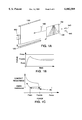
FIG. 18 is a side view of an embodiment of a mechanism in which the chip package may be inserted. A step by step demonstration of the mounting of the chip carrier on to a printed circuit board 1810 is shown. Two substantially parallel board mounted support rails 1820 are mounted to the printed circuit board 1810. The support rails 1820 are coupled to the printed circuit board 1810 by screws, an adhesive, or other means. The support rails are shaped to accept a chip package and hold it in place. For one embodiment, the support rails engage the cam followers 1870 of the chip package, and push the contacts of the chip package against traces on the printed circuit board 1810.
The printed circuit board 1810 further includes two substantially parallel board mounted rails of latches. A set of latches 1860 is associated with each support rail pair 1820. The latches 1860 keep the chip package in place, once the chip package is inserted into the support rails 1820. For one embodiment, the latches 1860 are molded plastic having a wedge shaped head, which is oriented to enable the chip packages to be inserted with ease and then hold the chip package against backward force.
The first chip package 1830 illustrated is being inserted into the support rail. The chip package 1830 is inserted at an angle. For one embodiment, that angle is approximately 10-15 degrees. When the chip package 1830 has made contact with the printed circuit board 1810, no further downward force is asserted.
The second chip package 1840 is being turned in the support rail. After an initial rotation the chip package 1840 makes contact with the printed circuit board. The chip package 1840 is rotated further to a substantially vertical position. The act of rotation wipes the contacts at the contact area of the chip package 1840. This wiping clears the contacts of surface film and debris, breaks the oxide barrier, and helps to ensure a better contact. For one embodiment, after an initial 5 degree rotation, the contacts are engaged, and the remaining 10 degrees of rotation is performs the wiping action.
The third chip package 1850 is illustrated in its vertical position. The chip package is supported by the support rail 1820 and is latched by the latches 1860. The chip package 1850 is held with a force of approximately 50-100 g/contact. The mounting mechanism shown is field replaceable, and supports the chip package 1850 in a vertically mounted position.
FIG. 19 is a top view of one chip package in the mounting mechanism of FIG. 18. The chip package 1850 is inserted between the support rails 1820. The support rails 1820 are substantially parallel and each engage one of the cam followers 1920 of the chip package 1850. The contacts 1930 of the chip package 1850 is in contact with the printed circuit board (not shown). The latches 1860 support the chip package 1850 and prevent it from slipping. The latches 1860 have a wedge shaped head 1910, which permits easy movement only in one direction. The chip package 1850 can be removed, but greater force has to be exerted. The force which the chip package 1850 exerts is not sufficient to move the latches 1860.
In the foregoing specification, the invention has been described with reference to specific embodiments thereof. It will, however, be evident that various modifications and changes may be made thereto without departing from the broader spirit and scope of the invention. The specification and drawings are, accordingly, to be regarded in an illustrative rather than a restrictive sense.

Claims (71)

What is claimed is:
1. An integrated circuit (IC) package for coupling to a printed circuit board, the IC package comprising:
a base having a side and a bottom;
a flex circuit coupled to the base wrapping around a portion of the side and the bottom of the base, and conforming to the base, the flex circuit having traces;
the traces on the flex circuit configured to be coupled to a plurality of leads of an integrated circuit, and the traces on the flex circuit further for coupling the IC package to the printed circuit board at the bottom of the base; and
the IC package configured to be coupled to the printed circuit board by engaging the printed circuit board with the base at an insertion angle with respect to the printed circuit board and rotating the base to a mounting angle with respect to the printed circuit board.
2. The integrated circuit package of claim 1 further comprising an elastomer coupled to the bottom of the base, the flex circuit contacting the elastomer.
3. The integrated circuit package of claim 2, wherein said elastomer has a compression set of less than 5%.
4. The integrated circuit package of claim 3 wherein another end of the flex circuit is glued to the base.
5. The integrated circuit package of claim 2 further comprising a slot in the base, the slot in the base receiving one end of the flex circuit.
6. The integrated circuit package of claim 2 wherein both ends of the flex circuit are glued to the base.
7. The integrated circuit package of claim 6 wherein said flex circuit is attached to the side of the base with a silver epoxy.
8. The integrated circuit package of claim 1 further comprising epoxy die attach, attaching the IC to the base.
9. The integrated circuit package of claim 1 wherein the traces on the flex circuit are fanned out between where the leads of the IC are coupled and where the integrated circuit package is coupled to the printed circuit board.
10. The integrated circuit package of claim 1 further comprising a solder on the traces of the flex circuit, the solder contacting the printed circuit board.
11. The integrated circuit package of claim 1 wherein the plurality of leads of the IC are soldered to the traces on the flex circuit.
12. The integrated circuit package of claim 1 wherein the plurality of leads of the IC are coupled via bonding wire to the traces on the flex circuit.
13. The integrated circuit package of claim 1 wherein the plurality of leads of the IC are a ball grid array, and the ball grid array is soldered to the traces on the flex circuit.
14. The integrated circuit package of claim 1 further comprising holes in the flex circuit, the holes for contacting ground wires to the base, the base acting as a ground plane.
15. The integrated circuit package of claim 1 further comprising encapsulation, encapsulating the IC.
16. The integrated circuit package of claim 15, wherein the encapsulation encapsulates the IC and the plurality of leads of the IC coupled to traces on the flex circuit.
17. The integrated circuit package of claim 1, further comprising a cam follower attached to the base, the cam follower for attaching the integrated circuit package into a chip file.
18. The integrated circuit package of claim 17, wherein said cam follower is integrally formed with the base.
19. The integrated circuit package of claim 1, wherein the base is made of zinc.
20. The integrated circuit package of claim 19, wherein the base is stamped.
21. The integrated circuit package of claim 1, wherein the base acts as a pressure plate and a heat spreader.
22. The integrated circuit page of claim 21, wherein the base further acts as a ground plane.
23. The integrated circuit package of claim 1, wherein the base is shaped like a J, the side of the base being a shaft of the J, and the bottom being a hook of the J.
24. The integrated circuit package of claim 23, wherein the hook of the J comprises a plurality of substantially parallel fingers.
25. The integrated circuit package of claim 23, wherein the base is made of a flexible metal.
26. The integrated circuit package of claim 25, wherein the base is made of BeCu.
27. The integrated circuit package of claim 1, further comprising a thin flexible layer coupled to the side of the base, and extending beyond the side of the base.
28. The integrated circuit package of claim 27, wherein the thin flexible layer comprises a thin metal layer and a thin insulating layer, the thin metal layer coupled to the base, and the thin insulating layer coupled to the flex circuit.
29. The integrated circuit package of claim 28 wherein the thin metal layer is made of BeCu.
30. The integrated circuit package of claim 28, wherein the thin insulating layer is a polyimide layer.
31. The integrated circuit package of claim 27, wherein said thin flexible layer forms a J shape, a shaft of the J attached to the base, and a hook of the J extending beyond the base and the hook of the J for coupling the integrated circuit package to the printed circuit board.
32. The integrated circuit package of claim 27, further comprising a conductive plate coupled to the traces of the flex circuit, the conductive plate contacting the printed circuit board.
33. The integrated circuit package of claim 1, further comprising a plurality of solder balls, the solder balls coupled to the traces of the flex circuit, the solder balls for coupling the integrated circuit package to the printed circuit board.
34. The integrated circuit package of claim 1, further comprising a bump in the flex circuit, the bump designed to reduce an area of contact between the integrated circuit package and the printed circuit board.
35. The integrated circuit package of claim 34, further comprising a conductive plate coupled to the traces on the flex circuit, for contacting a plate on the printed circuit board.
36. The integrated circuit package of claim 35, wherein the conductive plate is PbSn.
37. The package of claim 1 wherein the insertion angle is approximately 10-15 degrees from perpendicular to the printed circuit board.
38. The package of claim 1 wherein the mounting angle is about 90 degrees.
39. The package of claim 1 wherein the traces of the flex circuit for coupling the IC package to the printed circuit board are wiped during rotation of the base to the mounting angle.
40. An integrated circuit (IC) package for coupling an integrated circuit (IC) to a printed circuit board, the IC package comprising:
a base having a side and a bottom;
an elastomer having a curved shape coupled to the bottom of the base;
a flex circuit coupled to the base and the elastomer, and conforming to the base and the elastomer;
the IC coupled to the side of the base, and having leads, the leads of the IC coupled to traces on the flex circuit; and
the traces on the flex circuit coupled to traces on the printed circuit board, such that the IC package is coupled to the printed circuit board by engaging the printed circuit board with the base at an insertion angle with respect to the printed circuit board and rotating the base to a mounting angle with respect to the printed circuit board.
41. The integrated circuit package of claim 40 further comprising cam followers attached to the base, to fix the integrated circuit package to the printed circuit board.
42. The integrated circuit package of claim 40 further comprising solder coupled to the traces on the flex circuit, to provide point contacts with the traces on the printed circuit board.
43. The integrated circuit package of claim 42, wherein the point contacts are wiped when the integrated circuit package is inserted into a mounting mechanism.
44. The integrated circuit package of claim 40 wherein the base is made of approximately 42% nickel and 58% iron.
45. The integrated circuit package of claim 40 wherein the flex circuit is copper on polyimide.
46. The integrated circuit package of claim 40, wherein the elastomer is selected from the group of: fluorosilicon, silicon rubber or fluoroelastomer.
47. The integrated circuit package of claim 40, wherein the IC is a dynamic random access memory (DRAM).
48. The package of claim 40 wherein the insertion angle is approximately 10-15 degrees from perpendicular to the printed circuit board.
49. The package of claim 40 wherein the mounting angle is about 90 degrees.
50. The package of claim 40 wherein the traces of the flex circuit for coupling the IC package to the printed circuit board are wiped during rotation of the base to the mounting angle.
51. An integrated circuit (IC) package for coupling an integrated circuit to a printed circuit board, comprising:
a base having a bottom, a side, a first layer capable of having the integrated circuit coupled to it, and a second layer coupled to the first layer;
a flex circuit having traces therein, the flex circuit coupled to the base;
the IC package configured to be coupled to the printed circuit board by engaging the printed circuit board with the base at an insertion angle with respect to the printed circuit board and rotating the base to a mounting angle with respect to the printed circuit board; and
the traces for coupling to leads of the integrated circuit, and the traces further for coupling to traces on the printed circuit board.
52. The integrated circuit package of claim 50, wherein the first layer of the base is in the shape of an inverted L.
53. The integrated circuit package of claim 50, wherein the second layer of the base is in the shape of a J, a hook of the J extending beyond a bottom of the first layer.
54. The integrated circuit package of claim 53, wherein the hook of the J of the second layer comprises a plurality of substantially parallel prongs.
55. The integrated circuit package of claim 53, wherein the second layer of the base has a hole in it, the hole being substantially equal in size to a size of the integrated circuit, and the integrated circuit projecting through the hole in the second layer.
56. The integrated circuit package of claim 53 further comprising locking tabs, the locking tabs for interacting with a mounting mechanism of the printed circuit board, for fastening the integrated circuit package on the printed circuit board.
57. The integrated circuit package of claim 53, wherein the flex circuit is substantially conforming with hook of the J.
58. The integrated circuit package of claim 57, wherein the flex circuit further comprises a plurality of wire bond pads, the wire bond pads for coupling to the integrated circuit.
59. The integrated circuit package of claim 58, wherein the traces of the flex circuit are coupled via bonding wire to the leads of the integrated circuit.
60. The integrated circuit package of claim 50, wherein the flex circuit is in the shape of a U, and the flex circuit is coupled to the second layer of the base.
61. The integrated circuit package of claim 51, further comprising a location for a bypass capacitor on the flex circuit.
62. The integrated circuit package of claim 50 wherein the first layer is made of copper.
63. The integrated circuit package of claim 50 the first layer is made of approximately 42% nickel and 58% iron.
64. The integrated circuit package of claim 50 wherein the second layer is made of a flexible metal.
65. The integrated circuit package of claim 64 wherein the second layer is made of BeCu.
66. The integrated circuit package of claim 50 wherein the flex circuit is copper on polyimide.
67. The integrated circuit package of claim 50 further comprising an encapsulation for protecting the integrated circuit and a bonding wire coupling the integrated circuit and the traces on the flex circuit.
68. The integrated circuit package of claim 67, wherein the encapsulant is epoxy.
69. The package of claim 51 wherein the insertion angle is approximately 10-15 degrees from perpendicular to the printed circuit board.
70. The package of claim 51 wherein the mounting angle is about 90 degrees.
71. The package of claim 51 wherein the traces of the flex circuit for coupling the IC package to the printed circuit board are wiped during rotation of the base to the mounting angle.
US08/897,784 1997-07-21 1997-07-21 Integrated circuit package for coupling to a printed circuit board Expired - Lifetime US6002589A (en)

Priority Applications (4)

Application Number Priority Date Filing Date Title
US08/897,784 US6002589A (en) 1997-07-21 1997-07-21 Integrated circuit package for coupling to a printed circuit board
TW087111869A TW434860B (en) 1997-07-21 1998-07-21 Integrated circuit package
PCT/US1998/015056 WO1999004415A2 (en) 1997-07-21 1998-07-21 Integrated circuit package
US09/443,135 US6447321B1 (en) 1997-07-21 1999-11-18 Socket for coupling an integrated circuit package to a printed circuit board

Applications Claiming Priority (1)

Application Number Priority Date Filing Date Title
US08/897,784 US6002589A (en) 1997-07-21 1997-07-21 Integrated circuit package for coupling to a printed circuit board

Related Child Applications (1)

Application Number Title Priority Date Filing Date
US09/443,135 Division US6447321B1 (en) 1997-07-21 1999-11-18 Socket for coupling an integrated circuit package to a printed circuit board

Publications (1)

Publication Number Publication Date
US6002589A true US6002589A (en) 1999-12-14

Family

ID=25408414

Family Applications (2)

Application Number Title Priority Date Filing Date
US08/897,784 Expired - Lifetime US6002589A (en) 1997-07-21 1997-07-21 Integrated circuit package for coupling to a printed circuit board
US09/443,135 Expired - Fee Related US6447321B1 (en) 1997-07-21 1999-11-18 Socket for coupling an integrated circuit package to a printed circuit board

Family Applications After (1)

Application Number Title Priority Date Filing Date
US09/443,135 Expired - Fee Related US6447321B1 (en) 1997-07-21 1999-11-18 Socket for coupling an integrated circuit package to a printed circuit board

Country Status (3)

Country Link
US (2) US6002589A (en)
TW (1) TW434860B (en)
WO (1) WO1999004415A2 (en)

Cited By (34)

* Cited by examiner, † Cited by third party
Publication number Priority date Publication date Assignee Title
US20020093351A1 (en) * 2001-01-18 2002-07-18 Holcombe Brent A. Method for constructing a flex-rigid laminate probe
US6449159B1 (en) 2000-05-03 2002-09-10 Rambus Inc. Semiconductor module with imbedded heat spreader
US6469907B1 (en) 2000-10-23 2002-10-22 Team Pacific, Corporation Packaging for power and other circuitry
US20030109182A1 (en) * 2001-11-01 2003-06-12 Fujitsu Component Limited Contact module, connector and method of producing said contact module
US6589059B2 (en) * 1995-05-26 2003-07-08 Rambus, Inc. Chip socket assembly and chip file assembly for semiconductor chips
US6704204B1 (en) 1998-06-23 2004-03-09 Intel Corporation IC package with edge connect contacts
US20040229480A1 (en) * 2002-03-13 2004-11-18 Rambus, Inc. Memory module
US6833984B1 (en) 2000-05-03 2004-12-21 Rambus, Inc. Semiconductor module with serial bus connection to multiple dies
US20040262737A1 (en) * 2000-05-03 2004-12-30 Belgacem Haba Semiconductor module
US20050042894A1 (en) * 2003-08-21 2005-02-24 Li Xing Wu Electrical connection and component assembly for constitution of a hard disk drive
WO2005101490A2 (en) * 2004-04-19 2005-10-27 Siemens Aktiengesellschaft Component that is situated on a cooling fin
US20050245137A1 (en) * 2004-03-31 2005-11-03 Sang-Wook Park Memory module, socket and mounting method providing improved heat dissipating characteristics
US20060014402A1 (en) * 1995-05-26 2006-01-19 Perino Donald V Chip socket assembly and chip file assembly for semiconductor chips
US20060090102A1 (en) * 2004-09-03 2006-04-27 Wehrly James D Jr Circuit module with thermal casing systems and methods
US20070115017A1 (en) * 2004-09-03 2007-05-24 Staktek Group L.P. Thin Module System and Method
US20080293306A1 (en) * 2007-05-23 2008-11-27 Japan Aviation Electronics Industry, Limited Connector connectable with low contact pressure
US7656678B2 (en) 2001-10-26 2010-02-02 Entorian Technologies, Lp Stacked module systems
US7719098B2 (en) 2001-10-26 2010-05-18 Entorian Technologies Lp Stacked modules and method
US7737549B2 (en) 2004-09-03 2010-06-15 Entorian Technologies Lp Circuit module with thermal casing systems
US7760513B2 (en) 2004-09-03 2010-07-20 Entorian Technologies Lp Modified core for circuit module system and method
US7768796B2 (en) 2004-09-03 2010-08-03 Entorian Technologies L.P. Die module system
US7804985B2 (en) 2006-11-02 2010-09-28 Entorian Technologies Lp Circuit module having force resistant construction
CN105490671A (en) * 2014-10-01 2016-04-13 亚德诺半导体集团 High isolation wideband switch
USD824910S1 (en) * 2017-02-17 2018-08-07 Samsung Electronics Co., Ltd. SSD storage device
USD826945S1 (en) * 2017-02-17 2018-08-28 Samsung Electronics Co., Ltd. SSD storage device
USD826946S1 (en) * 2017-02-17 2018-08-28 Samsung Electronics Co., Ltd. SSD storage device
USD826944S1 (en) * 2017-02-17 2018-08-28 Samsung Electronics Co., Ltd. SSD storage device
USD828357S1 (en) * 2017-02-17 2018-09-11 Samsung Electronics Co., Ltd. SSD storage device
USD828358S1 (en) * 2017-02-17 2018-09-11 Samsung Electronics Co., Ltd. SSD storage device
USD834025S1 (en) * 2017-02-17 2018-11-20 Samsung Electronics Co., Ltd. SSD storage device
CN105490671B (en) * 2014-10-01 2019-07-16 亚德诺半导体集团 High-isolation wideband switch
US10587060B2 (en) 2017-11-30 2020-03-10 International Business Machines Corporation Electrical contacts on the sidewall of a circuit board
DE102019201808A1 (en) * 2019-02-12 2020-08-13 Festo Se & Co. Kg Module unit, module arrangement and connection establishment
US20230081254A1 (en) * 2021-09-16 2023-03-16 International Business Machines Corporation Cable bonding protection for head dimensional stability

Families Citing this family (8)

* Cited by examiner, † Cited by third party
Publication number Priority date Publication date Assignee Title
US6642136B1 (en) 2001-09-17 2003-11-04 Megic Corporation Method of making a low fabrication cost, high performance, high reliability chip scale package
US7099293B2 (en) 2002-05-01 2006-08-29 Stmicroelectronics, Inc. Buffer-less de-skewing for symbol combination in a CDMA demodulator
US7156678B2 (en) * 2005-04-07 2007-01-02 3M Innovative Properties Company Printed circuit connector assembly
US7374429B2 (en) * 2005-04-26 2008-05-20 3M Innovative Properties Company Connector assembly
US7033861B1 (en) * 2005-05-18 2006-04-25 Staktek Group L.P. Stacked module systems and method
US7338292B2 (en) * 2006-01-26 2008-03-04 Agilent Technologies, Inc. Board-to-board electronic interface using hemi-ellipsoidal surface features
US7906844B2 (en) * 2006-09-26 2011-03-15 Compass Technology Co. Ltd. Multiple integrated circuit die package with thermal performance
MY147054A (en) * 2008-03-07 2012-10-15 Joinset Co Ltd Solderable elastic electric contact terminal

Citations (44)

* Cited by examiner, † Cited by third party
Publication number Priority date Publication date Assignee Title
US3082398A (en) * 1960-05-24 1963-03-19 Amphenol Borg Electronics Corp Electrical connectors
US3114587A (en) * 1961-10-02 1963-12-17 Adolf L Herrmann Flat cables and corresponding connector
FR2109444A5 (en) * 1970-10-16 1972-05-26 Socapex
US3701071A (en) * 1971-01-18 1972-10-24 Berg Electronics Inc Hinge type circuit board connector block
US3874768A (en) * 1974-03-11 1975-04-01 John M Cutchaw Integrated circuit connector
JPS55138264A (en) * 1979-04-11 1980-10-28 Fujitsu Ltd Microwave integrated circuit package
US4426689A (en) * 1979-03-12 1984-01-17 International Business Machines Corporation Vertical semiconductor integrated circuit chip packaging
JPS59130453A (en) * 1983-01-17 1984-07-27 Nec Corp Package of semiconductor integrated circuit
US4586764A (en) * 1985-01-07 1986-05-06 Motorola, Inc. Electrical subassembly structure
US4598962A (en) * 1984-03-14 1986-07-08 Motorola, Inc. Memory device retaining apparatus for portable data processor
US4636022A (en) * 1985-03-11 1987-01-13 Thomas & Betts Corporation Cassette connector
US4678252A (en) * 1986-05-27 1987-07-07 Rockwell International Corporation Electrical connector for circuit boards
DE3611346A1 (en) * 1986-04-04 1987-10-08 Bbc Brown Boveri & Cie Device for vertical mounting of semiconductor components, especially transistors
US4714435A (en) * 1985-11-14 1987-12-22 Molex Incorporated Connection for flexible apparatus
US4795079A (en) * 1985-03-29 1989-01-03 Canon Kabushiki Kaisha Structure of joining printed circuit boards and process for producing the same
US4798541A (en) * 1987-09-02 1989-01-17 Ncr Corporation Right angle electrical connector
JPH01166545A (en) * 1987-12-22 1989-06-30 Nec Corp Zigzag type ic
US4850892A (en) * 1985-12-16 1989-07-25 Wang Laboratories, Inc. Connecting apparatus for electrically connecting memory modules to a printed circuit board
US4885126A (en) * 1986-10-17 1989-12-05 Polonio John D Interconnection mechanisms for electronic components
US4891023A (en) * 1988-08-22 1990-01-02 Molex Incorporated Circuit card edge connector and terminal therefor
US4939570A (en) * 1988-07-25 1990-07-03 International Business Machines, Corp. High power, pluggable tape automated bonding package
US4967262A (en) * 1989-11-06 1990-10-30 Micron Technology, Inc. Gull-wing zig-zag inline lead package having end-of-package anchoring pins
US4975763A (en) * 1988-03-14 1990-12-04 Texas Instruments Incorporated Edge-mounted, surface-mount package for semiconductor integrated circuit devices
US5002494A (en) * 1989-05-09 1991-03-26 Amp Incorporated Printed circuit board edge connector
US5026297A (en) * 1990-06-28 1991-06-25 Molex Incorporated Electrical socket assembly for single in-line circuit package
US5051366A (en) * 1990-10-01 1991-09-24 International Business Machines Corporation Electrical connector
EP0472203A1 (en) * 1990-08-23 1992-02-26 The Whitaker Corporation Dual readout SIMM socket
US5104324A (en) * 1991-06-26 1992-04-14 Amp Incorporated Multichip module connector
EP0542433A2 (en) * 1991-11-13 1993-05-19 Amphenol Corporation Connector
US5229916A (en) * 1992-03-04 1993-07-20 International Business Machines Corporation Chip edge interconnect overlay element
WO1993018559A1 (en) * 1992-03-06 1993-09-16 Augat Inc. Edge card interconnection system
US5260601A (en) * 1988-03-14 1993-11-09 Texas Instruments Incorporated Edge-mounted, surface-mount package for semiconductor integrated circuit devices
US5278724A (en) * 1992-07-06 1994-01-11 International Business Machines Corporation Electronic package and method of making same
US5337220A (en) * 1993-09-10 1994-08-09 The Whitaker Corporation Electronic card and connector assembly for use therewith
US5432678A (en) * 1994-05-12 1995-07-11 Texas Instruments Incorporated High power dissipation vertical mounted package for surface mount application
US5568363A (en) * 1992-05-12 1996-10-22 Kitahara; Akira Surface mount components and semifinished products thereof
US5569045A (en) * 1994-02-10 1996-10-29 Hsu; Fu-Yu Electrical connector
US5610642A (en) * 1993-04-30 1997-03-11 Hewlett-Packard Company Flex circuit with multiple trace configurations and method of manufacture
US5633533A (en) * 1995-07-26 1997-05-27 International Business Machines Corporation Electronic package with thermally conductive support member having a thin circuitized substrate and semiconductor device bonded thereto
US5673479A (en) * 1993-12-20 1997-10-07 Lsi Logic Corporation Method for mounting a microelectronic circuit peripherally-leaded package including integral support member with spacer
US5748209A (en) * 1994-10-31 1998-05-05 Hewlett-Packard Company Thermal ink jet tab circuit having a plurality of trace groups wherein adjacent traces in each group are staggered
JPH10150065A (en) * 1996-11-15 1998-06-02 Japan Aviation Electron Ind Ltd Chip-size package
US5790380A (en) * 1995-12-15 1998-08-04 International Business Machines Corporation Method for fabricating a multiple chip module using orthogonal reorientation of connection planes
US5903292A (en) * 1991-06-19 1999-05-11 Hewlett-Packard Company Ink refill techniques for an inkjet print cartridge which leave correct back pressure

Family Cites Families (3)

* Cited by examiner, † Cited by third party
Publication number Priority date Publication date Assignee Title
US4378139A (en) * 1981-07-14 1983-03-29 Wells Electronics, Inc. Integrated circuit carrier connector
JPS5931217A (en) 1982-08-13 1984-02-20 Suzunaka Kiki:Kk Automatic formation apparatus for fish-tray agglomerated body
DE3684763D1 (en) 1985-11-14 1992-05-14 Molex Inc ARRANGEMENT FOR ELECTRICALLY CONNECTING A FLEXIBLE CURRENT BRACKET TO ANOTHER CURRENT BRACKET.

Patent Citations (44)

* Cited by examiner, † Cited by third party
Publication number Priority date Publication date Assignee Title
US3082398A (en) * 1960-05-24 1963-03-19 Amphenol Borg Electronics Corp Electrical connectors
US3114587A (en) * 1961-10-02 1963-12-17 Adolf L Herrmann Flat cables and corresponding connector
FR2109444A5 (en) * 1970-10-16 1972-05-26 Socapex
US3701071A (en) * 1971-01-18 1972-10-24 Berg Electronics Inc Hinge type circuit board connector block
US3874768A (en) * 1974-03-11 1975-04-01 John M Cutchaw Integrated circuit connector
US4426689A (en) * 1979-03-12 1984-01-17 International Business Machines Corporation Vertical semiconductor integrated circuit chip packaging
JPS55138264A (en) * 1979-04-11 1980-10-28 Fujitsu Ltd Microwave integrated circuit package
JPS59130453A (en) * 1983-01-17 1984-07-27 Nec Corp Package of semiconductor integrated circuit
US4598962A (en) * 1984-03-14 1986-07-08 Motorola, Inc. Memory device retaining apparatus for portable data processor
US4586764A (en) * 1985-01-07 1986-05-06 Motorola, Inc. Electrical subassembly structure
US4636022A (en) * 1985-03-11 1987-01-13 Thomas & Betts Corporation Cassette connector
US4795079A (en) * 1985-03-29 1989-01-03 Canon Kabushiki Kaisha Structure of joining printed circuit boards and process for producing the same
US4714435A (en) * 1985-11-14 1987-12-22 Molex Incorporated Connection for flexible apparatus
US4850892A (en) * 1985-12-16 1989-07-25 Wang Laboratories, Inc. Connecting apparatus for electrically connecting memory modules to a printed circuit board
DE3611346A1 (en) * 1986-04-04 1987-10-08 Bbc Brown Boveri & Cie Device for vertical mounting of semiconductor components, especially transistors
US4678252A (en) * 1986-05-27 1987-07-07 Rockwell International Corporation Electrical connector for circuit boards
US4885126A (en) * 1986-10-17 1989-12-05 Polonio John D Interconnection mechanisms for electronic components
US4798541A (en) * 1987-09-02 1989-01-17 Ncr Corporation Right angle electrical connector
JPH01166545A (en) * 1987-12-22 1989-06-30 Nec Corp Zigzag type ic
US4975763A (en) * 1988-03-14 1990-12-04 Texas Instruments Incorporated Edge-mounted, surface-mount package for semiconductor integrated circuit devices
US5260601A (en) * 1988-03-14 1993-11-09 Texas Instruments Incorporated Edge-mounted, surface-mount package for semiconductor integrated circuit devices
US4939570A (en) * 1988-07-25 1990-07-03 International Business Machines, Corp. High power, pluggable tape automated bonding package
US4891023A (en) * 1988-08-22 1990-01-02 Molex Incorporated Circuit card edge connector and terminal therefor
US5002494A (en) * 1989-05-09 1991-03-26 Amp Incorporated Printed circuit board edge connector
US4967262A (en) * 1989-11-06 1990-10-30 Micron Technology, Inc. Gull-wing zig-zag inline lead package having end-of-package anchoring pins
US5026297A (en) * 1990-06-28 1991-06-25 Molex Incorporated Electrical socket assembly for single in-line circuit package
EP0472203A1 (en) * 1990-08-23 1992-02-26 The Whitaker Corporation Dual readout SIMM socket
US5051366A (en) * 1990-10-01 1991-09-24 International Business Machines Corporation Electrical connector
US5903292A (en) * 1991-06-19 1999-05-11 Hewlett-Packard Company Ink refill techniques for an inkjet print cartridge which leave correct back pressure
US5104324A (en) * 1991-06-26 1992-04-14 Amp Incorporated Multichip module connector
EP0542433A2 (en) * 1991-11-13 1993-05-19 Amphenol Corporation Connector
US5229916A (en) * 1992-03-04 1993-07-20 International Business Machines Corporation Chip edge interconnect overlay element
WO1993018559A1 (en) * 1992-03-06 1993-09-16 Augat Inc. Edge card interconnection system
US5568363A (en) * 1992-05-12 1996-10-22 Kitahara; Akira Surface mount components and semifinished products thereof
US5278724A (en) * 1992-07-06 1994-01-11 International Business Machines Corporation Electronic package and method of making same
US5610642A (en) * 1993-04-30 1997-03-11 Hewlett-Packard Company Flex circuit with multiple trace configurations and method of manufacture
US5337220A (en) * 1993-09-10 1994-08-09 The Whitaker Corporation Electronic card and connector assembly for use therewith
US5673479A (en) * 1993-12-20 1997-10-07 Lsi Logic Corporation Method for mounting a microelectronic circuit peripherally-leaded package including integral support member with spacer
US5569045A (en) * 1994-02-10 1996-10-29 Hsu; Fu-Yu Electrical connector
US5432678A (en) * 1994-05-12 1995-07-11 Texas Instruments Incorporated High power dissipation vertical mounted package for surface mount application
US5748209A (en) * 1994-10-31 1998-05-05 Hewlett-Packard Company Thermal ink jet tab circuit having a plurality of trace groups wherein adjacent traces in each group are staggered
US5633533A (en) * 1995-07-26 1997-05-27 International Business Machines Corporation Electronic package with thermally conductive support member having a thin circuitized substrate and semiconductor device bonded thereto
US5790380A (en) * 1995-12-15 1998-08-04 International Business Machines Corporation Method for fabricating a multiple chip module using orthogonal reorientation of connection planes
JPH10150065A (en) * 1996-11-15 1998-06-02 Japan Aviation Electron Ind Ltd Chip-size package

Non-Patent Citations (22)

* Cited by examiner, † Cited by third party
Title
"Chip To Package Interconnections", chapter from book: Optoelectronic Interconnections, pp. 436, 437 & 463.
Brearley, Jr., D. "Assuming Reliability of Surface Mounted Connectors," National Electronic Packaging and Production Conference, pp. 606-614 (Feb. 25-27, 1986).
Brearley, Jr., D. "The Connector/PCB Interface Key to Success in Surface Mounting of Connectors,"N.E.P. and Production Conference, pp. 427-434 (Feb. 25-27 1986).
Brearley, Jr., D. Assuming Reliability of Surface Mounted Connectors, National Electronic Packaging and Production Conference, pp. 606 614 (Feb. 25 27, 1986). *
Brearley, Jr., D. The Connector/PCB Interface Key to Success in Surface Mounting of Connectors, N.E.P. and Production Conference, pp. 427 434 (Feb. 25 27 1986). *
Chip To Package Interconnections , chapter from book: Optoelectronic Interconnections, pp. 436, 437 & 463. *
Choudhury, M. A. "Fasteners Take on New Shapes," Electronic Packaging & Production, pp. 58-59 (May 1986).
Choudhury, M. A. Fasteners Take on New Shapes, Electronic Packaging & Production, pp. 58 59 (May 1986). *
Cook, R. "More Memory in Less Space", Byte Magazine, pp. 197, 198, 200 (Jun. 1995).
Cook, R. More Memory in Less Space , Byte Magazine, pp. 197, 198, 200 (Jun. 1995). *
European Search Report, 1 page. *
Gates, M., "Supporting the Surface Mounting Switchover," New electronics, pp. 63, 65, 67 (Jun. 26, 1984).
Gates, M., Supporting the Surface Mounting Switchover, New electronics, pp. 63, 65, 67 (Jun. 26, 1984). *
Goel, R. P. "Greater Packaging Density Through Direct Surface Mounting of Components," pp. 17-20 (Dec. 1986).
Goel, R. P. Greater Packaging Density Through Direct Surface Mounting of Components, pp. 17 20 (Dec. 1986). *
IBM Technical Disclosure Bulletin "Inexpensive Chip Package" vol. 33 No. 1A pp.272 and 273, Jun. 1990.
IBM Technical Disclosure Bulletin Inexpensive Chip Package vol. 33 No. 1A pp.272 and 273, Jun. 1990. *
Janota, N. et al., "The Connectorization of Surface-Mount PC Boards," Design News, pp. 88-90 (Jun. 16, 1986).
Janota, N. et al., The Connectorization of Surface Mount PC Boards, Design News, pp. 88 90 (Jun. 16, 1986). *
Terry Cosslouc, Connector Combines Metal With Elastomers. 1 page. *
Timmins, D. L. "An Elastomeric Interconnect System for Fine Pitch Leadless Chip Carriers," IEEE 34th Electronic Components Conference, pp. 138-143 (May 14-16, 1984).
Timmins, D. L. An Elastomeric Interconnect System for Fine Pitch Leadless Chip Carriers, IEEE 34 th Electronic Components Conference, pp. 138 143 (May 14 16, 1984). *

Cited By (54)

* Cited by examiner, † Cited by third party
Publication number Priority date Publication date Assignee Title
US6589059B2 (en) * 1995-05-26 2003-07-08 Rambus, Inc. Chip socket assembly and chip file assembly for semiconductor chips
US20060014402A1 (en) * 1995-05-26 2006-01-19 Perino Donald V Chip socket assembly and chip file assembly for semiconductor chips
US8096812B2 (en) 1995-05-26 2012-01-17 Rambus Inc. Chip socket assembly and chip file assembly for semiconductor chips
US6704204B1 (en) 1998-06-23 2004-03-09 Intel Corporation IC package with edge connect contacts
US20040262737A1 (en) * 2000-05-03 2004-12-30 Belgacem Haba Semiconductor module
US20070230134A1 (en) * 2000-05-03 2007-10-04 Belgacem Haba Semiconductor Module with Serial Bus Connection to Multiple Dies
USRE42785E1 (en) 2000-05-03 2011-10-04 Rambus Inc. Semiconductor module with serial bus connection to multiple dies
US6833984B1 (en) 2000-05-03 2004-12-21 Rambus, Inc. Semiconductor module with serial bus connection to multiple dies
US7122889B2 (en) 2000-05-03 2006-10-17 Rambus, Inc. Semiconductor module
USRE42429E1 (en) 2000-05-03 2011-06-07 Rambus Inc. Semiconductor module with serial bus connection to multiple dies
USRE42318E1 (en) 2000-05-03 2011-05-03 Rambus Inc. Semiconductor module with serial bus connection to multiple dies
US20070223159A1 (en) * 2000-05-03 2007-09-27 Belgacem Haba Semiconductor Module with Serial Bus Connection to Multiple Dies
US20070222061A1 (en) * 2000-05-03 2007-09-27 Belgacem Haba Semiconductor Module With Serial Bus Connection to Multiple Dies
US6449159B1 (en) 2000-05-03 2002-09-10 Rambus Inc. Semiconductor module with imbedded heat spreader
US6469907B1 (en) 2000-10-23 2002-10-22 Team Pacific, Corporation Packaging for power and other circuitry
US20020093351A1 (en) * 2001-01-18 2002-07-18 Holcombe Brent A. Method for constructing a flex-rigid laminate probe
US7656678B2 (en) 2001-10-26 2010-02-02 Entorian Technologies, Lp Stacked module systems
US7719098B2 (en) 2001-10-26 2010-05-18 Entorian Technologies Lp Stacked modules and method
US7011556B2 (en) * 2001-11-01 2006-03-14 Fujitsu Component Limited Contact module, connector and method of producing said contact module
US20030109182A1 (en) * 2001-11-01 2003-06-12 Fujitsu Component Limited Contact module, connector and method of producing said contact module
US7012812B2 (en) 2002-03-13 2006-03-14 Rambus, Inc. Memory module
US20060114661A1 (en) * 2002-03-13 2006-06-01 Belgacem Haba Memory module
US20040229480A1 (en) * 2002-03-13 2004-11-18 Rambus, Inc. Memory module
US7417871B2 (en) 2002-03-13 2008-08-26 Rambus Inc. Memory module
US20050042894A1 (en) * 2003-08-21 2005-02-24 Li Xing Wu Electrical connection and component assembly for constitution of a hard disk drive
US7014474B2 (en) * 2003-08-21 2006-03-21 Sae Magnetics (H.K.) Ltd. Electrical connection and component assembly for constitution of a hard disk drive
US20050176271A1 (en) * 2003-08-21 2005-08-11 Li Xing Wu Electrical connection and component assembly for constitution of a hard disk drive
US7033187B2 (en) * 2003-08-21 2006-04-25 Sae Magnetics (H.K.) Ltd. Electrical connection and component assembly for constitution of a hard disk drive
US7485006B2 (en) * 2004-03-31 2009-02-03 Samsung Electronics Co. Ltd. Memory module, socket and mounting method providing improved heat dissipating characteristics
US20050245137A1 (en) * 2004-03-31 2005-11-03 Sang-Wook Park Memory module, socket and mounting method providing improved heat dissipating characteristics
WO2005101490A3 (en) * 2004-04-19 2006-04-13 Siemens Ag Component that is situated on a cooling fin
WO2005101490A2 (en) * 2004-04-19 2005-10-27 Siemens Aktiengesellschaft Component that is situated on a cooling fin
US7602613B2 (en) * 2004-09-03 2009-10-13 Entorian Technologies, Lp Thin module system and method
US7737549B2 (en) 2004-09-03 2010-06-15 Entorian Technologies Lp Circuit module with thermal casing systems
US7760513B2 (en) 2004-09-03 2010-07-20 Entorian Technologies Lp Modified core for circuit module system and method
US7768796B2 (en) 2004-09-03 2010-08-03 Entorian Technologies L.P. Die module system
US20060090102A1 (en) * 2004-09-03 2006-04-27 Wehrly James D Jr Circuit module with thermal casing systems and methods
US20070115017A1 (en) * 2004-09-03 2007-05-24 Staktek Group L.P. Thin Module System and Method
US7804985B2 (en) 2006-11-02 2010-09-28 Entorian Technologies Lp Circuit module having force resistant construction
US20080293306A1 (en) * 2007-05-23 2008-11-27 Japan Aviation Electronics Industry, Limited Connector connectable with low contact pressure
US7614884B2 (en) * 2007-05-23 2009-11-10 Japan Aviation Electronics Industry, Limited Connector connectable with low contact pressure
CN105490671A (en) * 2014-10-01 2016-04-13 亚德诺半导体集团 High isolation wideband switch
CN105490671B (en) * 2014-10-01 2019-07-16 亚德诺半导体集团 High-isolation wideband switch
USD826945S1 (en) * 2017-02-17 2018-08-28 Samsung Electronics Co., Ltd. SSD storage device
USD826946S1 (en) * 2017-02-17 2018-08-28 Samsung Electronics Co., Ltd. SSD storage device
USD826944S1 (en) * 2017-02-17 2018-08-28 Samsung Electronics Co., Ltd. SSD storage device
USD828357S1 (en) * 2017-02-17 2018-09-11 Samsung Electronics Co., Ltd. SSD storage device
USD828358S1 (en) * 2017-02-17 2018-09-11 Samsung Electronics Co., Ltd. SSD storage device
USD834025S1 (en) * 2017-02-17 2018-11-20 Samsung Electronics Co., Ltd. SSD storage device
USD824910S1 (en) * 2017-02-17 2018-08-07 Samsung Electronics Co., Ltd. SSD storage device
US10587060B2 (en) 2017-11-30 2020-03-10 International Business Machines Corporation Electrical contacts on the sidewall of a circuit board
DE102019201808A1 (en) * 2019-02-12 2020-08-13 Festo Se & Co. Kg Module unit, module arrangement and connection establishment
DE102019201808B4 (en) 2019-02-12 2022-12-01 Festo Se & Co. Kg Module unit and module arrangement
US20230081254A1 (en) * 2021-09-16 2023-03-16 International Business Machines Corporation Cable bonding protection for head dimensional stability

Also Published As

Publication number Publication date
WO1999004415A3 (en) 1999-04-08
US6447321B1 (en) 2002-09-10
TW434860B (en) 2001-05-16
WO1999004415A2 (en) 1999-01-28

Similar Documents

Publication Publication Date Title
US6002589A (en) Integrated circuit package for coupling to a printed circuit board
US6078500A (en) Pluggable chip scale package
US6975518B2 (en) Printed circuit board housing clamp
US8299598B2 (en) Grid array packages and assemblies including the same
US5959356A (en) Solder ball grid array carrier package with heat sink
US6750551B1 (en) Direct BGA attachment without solder reflow
US6843421B2 (en) Molded memory module and method of making the module absent a substrate support
JP2761153B2 (en) Connector for semiconductor device
US6031284A (en) Package body and semiconductor chip package using same
US6661103B2 (en) Apparatus for packaging flip chip bare die on printed circuit boards
US5990552A (en) Apparatus for attaching a heat sink to the back side of a flip chip package
JP3410396B2 (en) High performance integrated circuit chip package
US6178629B1 (en) Method of utilizing a replaceable chip module
US5805419A (en) Low-profile socketed packaging system with land-grid array and thermally conductive slug
US20080237840A1 (en) Flexible circuit electronic package with standoffs
US5767528A (en) Semiconductor device including pad portion for testing
US5686842A (en) Known good die test apparatus and method
EP1936686A3 (en) Semiconductor Device, Method for Manufacturing the same, and Method for Mounting the same
WO2008088461A1 (en) Lateral force countering load mechanism for lga sockets
US6392887B1 (en) PLGA-BGA socket using elastomer connectors
US5947751A (en) Production and test socket for ball grid array semiconductor package
US6320253B1 (en) Semiconductor device comprising a socket and method for forming same
US5942907A (en) Method and apparatus for testing dies
GB2422725A (en) Mounting an IC socket securely on a substrate
CN1071493C (en) Semiconductor apparatus

Legal Events

Date Code Title Description
AS Assignment

Owner name: RAMBUS INC., CALIFORNIA

Free format text: ASSIGNMENT OF ASSIGNORS INTEREST;ASSIGNORS:PERINO, DONALD V.;DILLON, NANCY DAVID, EXECUTOR OF THE ESTATE OF JOHN B. DILLON, DECEASED;REEL/FRAME:009149/0262;SIGNING DATES FROM 19980403 TO 19980414

STCF Information on status: patent grant

Free format text: PATENTED CASE

FEPP Fee payment procedure

Free format text: PAYOR NUMBER ASSIGNED (ORIGINAL EVENT CODE: ASPN); ENTITY STATUS OF PATENT OWNER: LARGE ENTITY

FPAY Fee payment

Year of fee payment: 4

FPAY Fee payment

Year of fee payment: 8

FPAY Fee payment

Year of fee payment: 12