US6001683A - Formation method of interconnection in semiconductor device - Google Patents
Formation method of interconnection in semiconductor device Download PDFInfo
- Publication number
- US6001683A US6001683A US08/655,122 US65512296A US6001683A US 6001683 A US6001683 A US 6001683A US 65512296 A US65512296 A US 65512296A US 6001683 A US6001683 A US 6001683A
- Authority
- US
- United States
- Prior art keywords
- interconnection
- forming
- semiconductor device
- metal
- film
- Prior art date
- Legal status (The legal status is an assumption and is not a legal conclusion. Google has not performed a legal analysis and makes no representation as to the accuracy of the status listed.)
- Expired - Lifetime
Links
Images


Classifications
-
- H—ELECTRICITY
- H10—SEMICONDUCTOR DEVICES; ELECTRIC SOLID-STATE DEVICES NOT OTHERWISE PROVIDED FOR
- H10B—ELECTRONIC MEMORY DEVICES
- H10B12/00—Dynamic random access memory [DRAM] devices
- H10B12/01—Manufacture or treatment
- H10B12/02—Manufacture or treatment for one transistor one-capacitor [1T-1C] memory cells
- H10B12/05—Making the transistor
-
- H—ELECTRICITY
- H01—ELECTRIC ELEMENTS
- H01L—SEMICONDUCTOR DEVICES NOT COVERED BY CLASS H10
- H01L21/00—Processes or apparatus adapted for the manufacture or treatment of semiconductor or solid state devices or of parts thereof
- H01L21/02—Manufacture or treatment of semiconductor devices or of parts thereof
- H01L21/04—Manufacture or treatment of semiconductor devices or of parts thereof the devices having at least one potential-jump barrier or surface barrier, e.g. PN junction, depletion layer or carrier concentration layer
- H01L21/18—Manufacture or treatment of semiconductor devices or of parts thereof the devices having at least one potential-jump barrier or surface barrier, e.g. PN junction, depletion layer or carrier concentration layer the devices having semiconductor bodies comprising elements of Group IV of the Periodic System or AIIIBV compounds with or without impurities, e.g. doping materials
- H01L21/28—Manufacture of electrodes on semiconductor bodies using processes or apparatus not provided for in groups H01L21/20 - H01L21/268
-
- H—ELECTRICITY
- H10—SEMICONDUCTOR DEVICES; ELECTRIC SOLID-STATE DEVICES NOT OTHERWISE PROVIDED FOR
- H10B—ELECTRONIC MEMORY DEVICES
- H10B99/00—Subject matter not provided for in other groups of this subclass
Definitions
- the present invention relates to a process for forming an interconnection in a semiconductor device, and relates more particularly, to a method of forming an interconnection in such a device by using a landing pad.
- Interconnection technology in a semiconductor device can be divided into two steps, i.e., formation of a contact hole and formation of an interconnection.
- the width of the interconnection line becomes more narrow.
- the horizontal size of the contact is reduced its vertical size is increased, which increases the aspect ratio of the contact.
- a metal interconnection needs to be multileveled to enable enhancing of the operation speed of a device and for reliability of the interconnection.
- filling of a contact hole is essential for planarization of an interdielectric layer.
- the filling techniques for filling contact holes in current multilevel interconnection formation processes consist mainly of either one of two methods. Such filling procedures usually involve either a physical vapor deposition method or a chemical vapor deposition (CVD) method.
- the physical vapor deposition (PVD) method involves depositing in the contact hole a metal such as aluminum, for example, by sputtering.
- a metal such as aluminum
- sputtering a metal such as aluminum
- the aspect ratio becomes increased by the reduction of a contact hole size to 1 ⁇ m or less, the coverage-step of a metal deposited on the contact hole is degraded.
- the CVD method of filling a contact hole is advantageous for obtaining an excellent step-coverage characteristic. But, the CVD method still presents difficulties when the method involves depositing aluminum in the contact hole.
- the new method comprises the steps of depositing aluminum by sputtering at a temperature and then reflowing the deposited aluminum at a high temperature of 500° C.-550° C.
- An object of the present invention is to provide a method of forming an interconnection using a landing pad for lowering an aspect ratio of a contact to permit an aluminum (Al) reflow process to be effectively applied to a contact which is horizontally narrow and vertically deep.
- a method of forming an interconnection in a semiconductor device having a memory cell portion and a peripheral circuit portion comprising the steps of:
- step d depositing a metal material film on the whole surface of a resultant of the step d), followed by filling the recess structure and the contact hole for landing pad formation;
- bitline and landing pad by eliminating from said substrate the metal compound film and the metal material film, except for the films in said recess structure and said contact hole, which are filled with said metal material film for bitline and landing pad formation;
- a preferred method for forming an interconnection further comprises the steps of depositing spin-on glass (SOG) on the whole surface of the first insulating film and then eliminating the SOG and a part of the first insulating film by a full etchback method, after the step a) of depositing a first insulating film.
- SOG spin-on glass
- the landing pad is concurrently formed on the peripheral circuit portion.
- Such concurrent formation has the effect of reducing the thickness of an insulating film that can be obtained during a successive step of forming a contact hole for interconnection. Therefore, it is easy to etch the insulating film in forming the contact hole and a contact hole having a small aspect ratio can be formed on the landing pad.
- the above mentioned process according to the invention makes it easier to fill the contact hole for interconnection by the Al reflow method when forming a metal interconnection layer. Further, the step-coverage of a metal deposited on the contact hole for interconnection is enhanced and contact resistance is reduced. Thus, the reliability of a semiconductor device is increased by producing by such a process.
- FIG. 1 is a cross-sectional view of a memory cell portion of a semiconductor device process substrate resulting from an interconnection process step, wherein a first insulating film has been etched to form a groove and a direct contact hole.
- FIG. 2 is a cross-sectional view of a memory cell portion of a semiconductor device process substrate resulting from an interconnection process step, wherein an ohmic contact layer has been deposited in the contact hole.
- FIG. 3 is a cross-sectional view of a memory cell portion of a semiconductor device process substrate resulting from an interconnection process step, wherein a diffusion barrier film is deposited on the surface of the substrate including the surfaces of the contact hole and the ohmic layer.
- FIG. 4 is a cross-sectional view of a memory cell portion of a semiconductor device process substrate resulting from an interconnection process step, wherein a metal material film is deposited over the whole surface of the structure and also filling the contact hole.
- FIG. 5 is a cross-sectional view of a memory cell portion of a semiconductor device process substrate resulting from an interconnection process step, wherein a bitline has been formed in the substrate.
- FIG. 6 is a cross-sectional view of a memory cell portion of a semiconductor device process substrate resulting from an interconnection process step, wherein a film layer has been formed on the surface of the substrate such that the bitline is also covered with the film layer.
- FIG. 7 is a cross-sectional view of a memory cell portion of a semiconductor device process substrate resulting from an interconnection process step, wherein an upper and lower electrode have been formed upon the film layer such that the lower electrode extends down through the film layer and the first the first insulating film layer, extending all the way down the silicon substrate layer.
- FIG. 8 is a cross-sectional view of a memory cell portion of a semiconductor device process substrate resulting from an interconnection process step, wherein a second insulating layer has been deposited upon the substrate which layer covers the upper electrode surface.
- FIG. 9 is a cross-sectional view of a memory cell portion a semiconductor device process substrate resulting from an interconnection process step, corresponding to the step of FIG. 20.
- FIG. 10 is a cross-sectional view of a memory cell portion of a semiconductor device process substrate resulting from an interconnection process step, wherein a conductive metal layer is deposited on the surface of the substrate by a sputtering step.
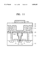
- FIG. 11 is a cross-sectional view of a memory cell portion of a semiconductor device process substrate resulting from an interconnection process step, wherein the top surface of the substrate has been etched to remove part of the top metal layer for patterned interconnectivity.
- FIG. 12 is a cross-sectional view of a peripheral circuit portion of an active region of a memory cell portion of a semiconductor device process substrate resulting from an interconnection process step, wherein a first insulating film has been etched to form a contact hole for landing pad formation.
- FIG. 13 is a cross-sectional view of a peripheral circuit portion of a semiconductor device process substrate resulting from an interconnection process step, wherein an ohmic contact layer has been deposited in the contact hole.
- FIG. 14 is a cross-sectional view of a peripheral circuit portion of a semiconductor device process substrate resulting from an interconnection process step, wherein a diffusion barrier film is deposited on the surface of the substrate including the surfaces of the contact hole and the ohmic layer.
- FIG. 15 is a cross-sectional view of a peripheral circuit portion of a semiconductor device process substrate resulting from an interconnection process step, wherein a metal material film is deposited over the whole surface of the structure and also filling the contact hole.
- FIG. 16 is a cross-sectional view of a peripheral circuit portion of a semiconductor device process substrate resulting from an interconnection process step, wherein a landing pad has been formed in the substrate.
- FIG. 17 is a cross-sectional view of a peripheral circuit portion of a semiconductor device process substrate resulting from an interconnection process step, wherein a SiN film layer has been formed on the surface of the substrate such that the landing pad is also covered with the film layer.
- FIG. 18 is a cross-sectional view of a peripheral circuit portion of a semiconductor device process substrate resulting from an interconnection process step, wherein the SiN film of the peripheral portion of the substrate has been eliminated.
- FIG. 19 is a cross-sectional view of a peripheral circuit portion of a semiconductor device process substrate resulting from an interconnection process step, wherein a second insulating layer has been deposited upon the substrate and the layer covers the top of the landing pad area.
- FIG. 20 is a cross-sectional view of a peripheral circuit portion of a semiconductor device process substrate resulting from an interconnection process step, wherein the second insulating film layer on the landing pad has been etched to produce a contact hole for an interconnection.
- FIG. 21 is a cross-sectional view of a peripheral circuit portion of a semiconductor device process substrate resulting from an interconnection process step, wherein a conductive metal layer is deposited by a sputtering step onto the surface of the substrate and into the contact hole of the landing pad.
- FIG. 22 is a cross-sectional view of a peripheral circuit portion of a semiconductor device process substrate resulting from an interconnection process step, wherein the top surface of the substrate has been etched to remove part of the top metal layer and form an interconnection line for patterned interconnectivity.
- FIGS. 1 through 11 are cross-sectional views of a memory cell portion in respective steps of a process for forming an interconnection in a semiconductor device according to an embodiment of the present invention.
- FIGS. 12 through 22 are cross-sectional views of a peripheral circuit portion in respective steps of a process for forming an interconnection in a semiconductor device.
- FIGS. 1 and 12 there is shown a cross section of a semiconductor device having a gate electrode 14, an active region 12a of a memory cell portion and an active region 12b of a peripheral circuit portion, i.e., source and drain regions are formed on a silicon substrate 10 in a usual manner.
- the substrates shown in FIGS. 1 and 12 contain first insulating film layers 16 of, for example, borophospho-silicate glass (BPSG) or undoped SiO 2 glass (USG), which are deposited by chemical vapor deposition (CVD).
- BPSG borophospho-silicate glass
- USG undoped SiO 2 glass
- the whole surface of the resultant structure is planarized by being coated with spin on glass (SOG), then planarized by eliminating the SOG and a part of first insulating film 16 by plasma full etchback.
- the first insulating film can be planarized by chemical mechanical polishing (CMP).
- CMP chemical mechanical polishing
- bitline of the memory cell portion is formed by dual-damascene.
- the whole surface of the resultant structure is patterned reversely to the bitline patterning, then first insulating film 16 is etched to an approximately 0.4 ⁇ m depth in a usual manner, to thereby form a groove 18.
- First insulating film 16 is re-etched by photolithography and etching so that a direct contact hole 20a is formed under groove 18 in order to be connected to an N-type active region 12a of the memory cell portion and at the same time a contact hole 20b for landing pad formation is formed in order to be connected to an N-type or P-type active region 12b of the peripheral circuit portion.
- a recess structure for the bitline of the memory cell portion consists of a direct contact hole 20a and groove 18.
- a metal film 22 for ohmic contact is deposited with Ti on the whole surface of the resultant structure by using sputtering.
- the metal film 22 for ohmic contact can be formed of one or more of W, Mo, Ta or Zr.
- metal film 22 for ohmic contact i.e., a Ti film is reacted with silicon on the surface of semiconductor substrate 10 under direct contact hole 20a and contact hole 20b for landing pad formation, to thereby selectively form a TiSi ohmic contact layer 24.
- the resultant structure is thermally treated by rapid thermal annealing (RTA) in an N 2 or Ar atmosphere, for 10-30 seconds at 500° C.-700° C., then a non-reacted portion of Ti film 22 is stripped by sulfuric acid or other chemical solution.
- RTA rapid thermal annealing
- TiSi ohmic contact layer 24 is thermally treated by RTA in an N 2 or Ar atmosphere, for 10-30 seconds at 700° C.-950° C. to be changed into C54-TiSi 2 , which is stable and has high electrical conductivity.
- a diffusion barrier film 26 is deposited on the whole surface of the resultant structure by reactive sputtering to a 200 ⁇ -1,000 ⁇ thickness, to thereby form a diffusion barrier film 26.
- a diffusion barrier film 26 can be formed of either a refractory metal nitride such as WN, TaN and ZrN, or a refractory metal carbide such as TiC, WC, TaC and ZrC.
- a metal material film 28 is formed by depositing a refractory metal such as W, Mo, Ta, Ti and Zr, which is not easily oxidized at a high temperature, on the whole surface of the resultant structure by CVD to a 1,000 ⁇ -5,000 ⁇ thickness.
- a refractory metal such as W, Mo, Ta, Ti and Zr
- the recess structure consisting of groove 18 and direct contact hole 20a, and contact hole 20b for landing pad formation are filled.
- the refractory metal can be replaced with the refractory metal compound.
- the refractory metal or the refractory metal compound such as the refractory metal nitride or the refractory metal carbide is used for forming the bitline, instead of usual polycide, so that a contact can be concurrently formed on active regions of an N-type and a P-type.
- diffusion barrier film 26 and a metal material film 28 are eliminated by chemical mechanical polishing (CMP) or plasma full etchback, to thereby form a bitline 30a and a landing pad 30b.
- CMP chemical mechanical polishing
- a SiN film 32 is formed on the whole surface of the resultant structure. As shown in FIG. 7, a lower electrode 34 of a capacitor, a Ta 2 O 5 dielectric film (not shown) and an upper electrode 36 are formed on the memory cell portion in a usual capacitor formation method. The SiN film 32 of the peripheral portion is eliminated as shown in FIG. 18.
- a second insulating film 38 is deposited on the whole surface of the resultant structure.
- a contact hole 40 for interconnection is formed by etching second insulating film 38 on landing pad 30b formed on the peripheral portion.
- the oxidized refractory metal film of a surface of exposed landing pad 30b under contact hole 40 for interconnection is eliminated by sputtering etching (or the refractory metal film is eliminated, then a barrier metal is deposited). Further, a metal layer 42 for interconnection is formed by depositing Al having high conductivity on the whole surface of the resultant structure, to thereby fill contact hole 40 for interconnection. In this process step, metal layer 42 for interconnection can be formed of a metal such as Cu. Ag or Au, or a metal compound such as Al-Cu, Al-Si-Cu or Ag-Cu.
- an Al reflow method for filling contact hole 40 for interconnection with Al, an Al reflow method, a high temperature sputtering method or a chemical vapor deposition method can be used.
- the Al reflow method is used for such a process step, but the other methods can be also used.
- a compound of Al-Si-Cu is deposited to a thickness of 2,000 ⁇ -6,000 ⁇ below 100° C., then maintained at 0.6 times higher than the melting point of the Al, preferably at a higher temperature than 450° C., for 30-180 seconds in a vacuum state to induce the movement of metal atoms so that the contact hole 40 for interconnection is filled.
- the peripheral circuit portion has a contact formed for interconnection by uniting landing pad 30b filled with the refractory metal (or a refractory metal compound) with the contact hole 40 which is filled with Al.
- a metal layer 42 for interconnection is patterned by photolithography and etching, to thereby form an interconnection line 42a.
- the landing pad which is filled with the refractory metal is concurrently formed on the peripheral circuit portion.
- Such a concurrent formation step has the effect of reducing the thickness of an insulating film that can be obtained during a successive step of forming a contact hole for interconnection. Therefore, it is easier to etch the contact hole for interconnection and a contact hole having a small aspect ratio is also formed on the landing pad.
- the contact hole for interconnection is easily filled by the Al reflow method when forming a metal interconnection layer, further the coverage-step of depositing a metal on the contact hole for interconnection is enhanced, contact resistance is reduced. Thus, the reliability of the semiconductor device is increased.
Abstract
A method of forming an interconnection by using a landing pad is disclosed. In a semiconductor device having a memory cell portion and a peripheral circuit portion, a refractory metal is used for the bitline instead of the usual polycide, to concurrently form a contact on each active region of an N-type and a P-type, then a landing pad is formed on the peripheral circuit portion when a bitline is formed on the memory cell portion. In such a process, a substantial contact hole for the interconnection is formed on the landing pad so that an aspect ratio of the contact can be lowered. Accordingly, when forming a metal interconnection, the contact hole for the interconnection is easily filled by Al reflow so that the coverage-step of the metal being depositing in the contact hole for the interconnection is enhanced, the contact resistance is reduced. Further, the reliability of the semiconductor device is improved.
Description
The present invention relates to a process for forming an interconnection in a semiconductor device, and relates more particularly, to a method of forming an interconnection in such a device by using a landing pad.
Interconnection technology in a semiconductor device can be divided into two steps, i.e., formation of a contact hole and formation of an interconnection. As a semiconductor device becomes highly-integrated, the width of the interconnection line becomes more narrow. When the horizontal size of the contact is reduced its vertical size is increased, which increases the aspect ratio of the contact. A metal interconnection needs to be multileveled to enable enhancing of the operation speed of a device and for reliability of the interconnection. Also, filling of a contact hole is essential for planarization of an interdielectric layer.
The filling techniques for filling contact holes in current multilevel interconnection formation processes consist mainly of either one of two methods. Such filling procedures usually involve either a physical vapor deposition method or a chemical vapor deposition (CVD) method.
The physical vapor deposition (PVD) method involves depositing in the contact hole a metal such as aluminum, for example, by sputtering. However, when the aspect ratio becomes increased by the reduction of a contact hole size to 1 μm or less, the coverage-step of a metal deposited on the contact hole is degraded.
The CVD method of filling a contact hole is advantageous for obtaining an excellent step-coverage characteristic. But, the CVD method still presents difficulties when the method involves depositing aluminum in the contact hole.
Accordingly, a new method for filling the contact hole has recently been proposed. The new method comprises the steps of depositing aluminum by sputtering at a temperature and then reflowing the deposited aluminum at a high temperature of 500° C.-550° C.
However, as the aspect ratio of the contact hole becomes increased due to high-integration of a semiconductor, such as to 256M DRAM and 1 G DRAM, it is difficult to fill the contact hole. This difficulty is present even when the new aluminum reflow method is used to fill the contact hole for the formation of the metal interconnection layer.
Accordingly, due to the difficulties in filling the contact holes, the step-coverage of the metal interconnection is degraded and the contact resistances are increased.
An object of the present invention is to provide a method of forming an interconnection using a landing pad for lowering an aspect ratio of a contact to permit an aluminum (Al) reflow process to be effectively applied to a contact which is horizontally narrow and vertically deep.
To accomplish the above object of the present invention, there is provided a method of forming an interconnection in a semiconductor device having a memory cell portion and a peripheral circuit portion, comprising the steps of:
a) forming an active region of the memory cell portion, forming an active region of the peripheral circuit portion and forming a gate electrode on a silicon substrate, and then depositing a first insulating film on the whole surface of the resultant structure;
b) forming a recess structure connected to the active region of the memory cell portion and a contact hole for landing pad formation connected to the active region of the peripheral circuit portion by etching the first insulating film;
c) depositing a metal film for ohmic contact on the whole surface of a resultant of the step b);
d) depositing a metal compound film for a diffusion barrier on the whole surface of a resultant of the step c);
e) depositing a metal material film on the whole surface of a resultant of the step d), followed by filling the recess structure and the contact hole for landing pad formation;
f) forming a bitline and a landing pad by eliminating from said substrate the metal compound film and the metal material film, except for the films in said recess structure and said contact hole, which are filled with said metal material film for bitline and landing pad formation;
g) depositing a second insulating film on the whole surface of a resultant of the step f);
h) forming a contact hole for interconnection by etching the second insulating film on the landing pad;
i) depositing a metal for interconnection on the whole surface of a resultant of the step h), followed by filling the contact hole for interconnection; and
j) forming an interconnection by patterning the metal for interconnection.
A preferred method for forming an interconnection further comprises the steps of depositing spin-on glass (SOG) on the whole surface of the first insulating film and then eliminating the SOG and a part of the first insulating film by a full etchback method, after the step a) of depositing a first insulating film.
It is further preferable in the above mentioned process according to the invention to include a step of selectively forming an ohmic contact layer on the surface of the silicon substrate by reacting the metal film for ohmic contact with silicon and then stripping a non-reacted part of the metal film for ohmic contact, after the step c) of depositing a metal film for ohmic contact.
According to the method of forming an interconnection of the above-mentioned present invention, when the bitline of the memory cell portion is formed during manufacturing a memory device, in particular when manufacturing a DRAM, the landing pad is concurrently formed on the peripheral circuit portion. Such concurrent formation has the effect of reducing the thickness of an insulating film that can be obtained during a successive step of forming a contact hole for interconnection. Therefore, it is easy to etch the insulating film in forming the contact hole and a contact hole having a small aspect ratio can be formed on the landing pad.
The above mentioned process according to the invention makes it easier to fill the contact hole for interconnection by the Al reflow method when forming a metal interconnection layer. Further, the step-coverage of a metal deposited on the contact hole for interconnection is enhanced and contact resistance is reduced. Thus, the reliability of a semiconductor device is increased by producing by such a process.
The above object and advantages of the present invention will become more apparent by describing in detail preferred embodiments thereof with reference to the attached drawings in which:
FIG. 1 is a cross-sectional view of a memory cell portion of a semiconductor device process substrate resulting from an interconnection process step, wherein a first insulating film has been etched to form a groove and a direct contact hole.
FIG. 2 is a cross-sectional view of a memory cell portion of a semiconductor device process substrate resulting from an interconnection process step, wherein an ohmic contact layer has been deposited in the contact hole.
FIG. 3 is a cross-sectional view of a memory cell portion of a semiconductor device process substrate resulting from an interconnection process step, wherein a diffusion barrier film is deposited on the surface of the substrate including the surfaces of the contact hole and the ohmic layer.
FIG. 4 is a cross-sectional view of a memory cell portion of a semiconductor device process substrate resulting from an interconnection process step, wherein a metal material film is deposited over the whole surface of the structure and also filling the contact hole.
FIG. 5 is a cross-sectional view of a memory cell portion of a semiconductor device process substrate resulting from an interconnection process step, wherein a bitline has been formed in the substrate.
FIG. 6 is a cross-sectional view of a memory cell portion of a semiconductor device process substrate resulting from an interconnection process step, wherein a film layer has been formed on the surface of the substrate such that the bitline is also covered with the film layer.
FIG. 7 is a cross-sectional view of a memory cell portion of a semiconductor device process substrate resulting from an interconnection process step, wherein an upper and lower electrode have been formed upon the film layer such that the lower electrode extends down through the film layer and the first the first insulating film layer, extending all the way down the silicon substrate layer.
FIG. 8 is a cross-sectional view of a memory cell portion of a semiconductor device process substrate resulting from an interconnection process step, wherein a second insulating layer has been deposited upon the substrate which layer covers the upper electrode surface.
FIG. 9 is a cross-sectional view of a memory cell portion a semiconductor device process substrate resulting from an interconnection process step, corresponding to the step of FIG. 20.
FIG. 10 is a cross-sectional view of a memory cell portion of a semiconductor device process substrate resulting from an interconnection process step, wherein a conductive metal layer is deposited on the surface of the substrate by a sputtering step.
FIG. 11 is a cross-sectional view of a memory cell portion of a semiconductor device process substrate resulting from an interconnection process step, wherein the top surface of the substrate has been etched to remove part of the top metal layer for patterned interconnectivity.
FIG. 12 is a cross-sectional view of a peripheral circuit portion of an active region of a memory cell portion of a semiconductor device process substrate resulting from an interconnection process step, wherein a first insulating film has been etched to form a contact hole for landing pad formation.
FIG. 13 is a cross-sectional view of a peripheral circuit portion of a semiconductor device process substrate resulting from an interconnection process step, wherein an ohmic contact layer has been deposited in the contact hole.
FIG. 14 is a cross-sectional view of a peripheral circuit portion of a semiconductor device process substrate resulting from an interconnection process step, wherein a diffusion barrier film is deposited on the surface of the substrate including the surfaces of the contact hole and the ohmic layer.
FIG. 15 is a cross-sectional view of a peripheral circuit portion of a semiconductor device process substrate resulting from an interconnection process step, wherein a metal material film is deposited over the whole surface of the structure and also filling the contact hole.
FIG. 16 is a cross-sectional view of a peripheral circuit portion of a semiconductor device process substrate resulting from an interconnection process step, wherein a landing pad has been formed in the substrate.
FIG. 17 is a cross-sectional view of a peripheral circuit portion of a semiconductor device process substrate resulting from an interconnection process step, wherein a SiN film layer has been formed on the surface of the substrate such that the landing pad is also covered with the film layer.
FIG. 18 is a cross-sectional view of a peripheral circuit portion of a semiconductor device process substrate resulting from an interconnection process step, wherein the SiN film of the peripheral portion of the substrate has been eliminated.
FIG. 19 is a cross-sectional view of a peripheral circuit portion of a semiconductor device process substrate resulting from an interconnection process step, wherein a second insulating layer has been deposited upon the substrate and the layer covers the top of the landing pad area.
FIG. 20 is a cross-sectional view of a peripheral circuit portion of a semiconductor device process substrate resulting from an interconnection process step, wherein the second insulating film layer on the landing pad has been etched to produce a contact hole for an interconnection.
FIG. 21 is a cross-sectional view of a peripheral circuit portion of a semiconductor device process substrate resulting from an interconnection process step, wherein a conductive metal layer is deposited by a sputtering step onto the surface of the substrate and into the contact hole of the landing pad.
FIG. 22 is a cross-sectional view of a peripheral circuit portion of a semiconductor device process substrate resulting from an interconnection process step, wherein the top surface of the substrate has been etched to remove part of the top metal layer and form an interconnection line for patterned interconnectivity.
The above object and advantages of the present invention will become more apparent by describing in detail a preferred embodiment thereof with reference to the attached drawings.
A first embodiment of the present invention is illustrated by FIGS. 1 through 11, which are cross-sectional views of a memory cell portion in respective steps of a process for forming an interconnection in a semiconductor device according to an embodiment of the present invention. Also, an example of the second embodiment of the present invention is illustrated by FIGS. 12 through 22, which are cross-sectional views of a peripheral circuit portion in respective steps of a process for forming an interconnection in a semiconductor device.
Referring to FIGS. 1 and 12, there is shown a cross section of a semiconductor device having a gate electrode 14, an active region 12a of a memory cell portion and an active region 12b of a peripheral circuit portion, i.e., source and drain regions are formed on a silicon substrate 10 in a usual manner. Also, the substrates shown in FIGS. 1 and 12 contain first insulating film layers 16 of, for example, borophospho-silicate glass (BPSG) or undoped SiO2 glass (USG), which are deposited by chemical vapor deposition (CVD). The whole surface of the resultant structure is planarized by being coated with spin on glass (SOG), then planarized by eliminating the SOG and a part of first insulating film 16 by plasma full etchback. In such a process, the first insulating film can be planarized by chemical mechanical polishing (CMP).
Then, a bitline of the memory cell portion is formed by dual-damascene. The whole surface of the resultant structure is patterned reversely to the bitline patterning, then first insulating film 16 is etched to an approximately 0.4 μm depth in a usual manner, to thereby form a groove 18.
First insulating film 16 is re-etched by photolithography and etching so that a direct contact hole 20a is formed under groove 18 in order to be connected to an N-type active region 12a of the memory cell portion and at the same time a contact hole 20b for landing pad formation is formed in order to be connected to an N-type or P-type active region 12b of the peripheral circuit portion. Accordingly, a recess structure for the bitline of the memory cell portion consists of a direct contact hole 20a and groove 18. Then, a metal film 22 for ohmic contact is deposited with Ti on the whole surface of the resultant structure by using sputtering. In this case, the metal film 22 for ohmic contact can be formed of one or more of W, Mo, Ta or Zr.
Referring to FIGS. 2 and 13, metal film 22 for ohmic contact, i.e., a Ti film is reacted with silicon on the surface of semiconductor substrate 10 under direct contact hole 20a and contact hole 20b for landing pad formation, to thereby selectively form a TiSi ohmic contact layer 24.
Subsequently, the resultant structure is thermally treated by rapid thermal annealing (RTA) in an N2 or Ar atmosphere, for 10-30 seconds at 500° C.-700° C., then a non-reacted portion of Ti film 22 is stripped by sulfuric acid or other chemical solution.
TiSi ohmic contact layer 24 is thermally treated by RTA in an N2 or Ar atmosphere, for 10-30 seconds at 700° C.-950° C. to be changed into C54-TiSi2, which is stable and has high electrical conductivity.
Referring to FIGS. 3 and 14, TiN is deposited on the whole surface of the resultant structure by reactive sputtering to a 200 Å-1,000 Å thickness, to thereby form a diffusion barrier film 26. Such a diffusion barrier film 26 can be formed of either a refractory metal nitride such as WN, TaN and ZrN, or a refractory metal carbide such as TiC, WC, TaC and ZrC.
Referring to FIGS. 4 and 15, a metal material film 28 is formed by depositing a refractory metal such as W, Mo, Ta, Ti and Zr, which is not easily oxidized at a high temperature, on the whole surface of the resultant structure by CVD to a 1,000 Å-5,000 Å thickness.
The recess structure consisting of groove 18 and direct contact hole 20a, and contact hole 20b for landing pad formation are filled. In such a step, the refractory metal can be replaced with the refractory metal compound.
The refractory metal or the refractory metal compound such as the refractory metal nitride or the refractory metal carbide is used for forming the bitline, instead of usual polycide, so that a contact can be concurrently formed on active regions of an N-type and a P-type.
Referring to FIGS. 5 and 16, diffusion barrier film 26 and a metal material film 28 (except for the recess structure and the contact hole 20b for forming a filled landing pad and a bitline) are eliminated by chemical mechanical polishing (CMP) or plasma full etchback, to thereby form a bitline 30a and a landing pad 30b.
Referring to FIGS. 6, 7, 17, and 18, a SiN film 32 is formed on the whole surface of the resultant structure. As shown in FIG. 7, a lower electrode 34 of a capacitor, a Ta2 O5 dielectric film (not shown) and an upper electrode 36 are formed on the memory cell portion in a usual capacitor formation method. The SiN film 32 of the peripheral portion is eliminated as shown in FIG. 18.
Referring to FIGS. 8 and 19, a second insulating film 38 is deposited on the whole surface of the resultant structure.
Referring to FIGS. 9 and 20, a contact hole 40 for interconnection is formed by etching second insulating film 38 on landing pad 30b formed on the peripheral portion.
Referring to FIGS. 10 and 21, the oxidized refractory metal film of a surface of exposed landing pad 30b under contact hole 40 for interconnection is eliminated by sputtering etching (or the refractory metal film is eliminated, then a barrier metal is deposited). Further, a metal layer 42 for interconnection is formed by depositing Al having high conductivity on the whole surface of the resultant structure, to thereby fill contact hole 40 for interconnection. In this process step, metal layer 42 for interconnection can be formed of a metal such as Cu. Ag or Au, or a metal compound such as Al-Cu, Al-Si-Cu or Ag-Cu.
For filling contact hole 40 for interconnection with Al, an Al reflow method, a high temperature sputtering method or a chemical vapor deposition method can be used. In the present invention the Al reflow method is used for such a process step, but the other methods can be also used.
According to the Al reflow method, a compound of Al-Si-Cu is deposited to a thickness of 2,000 Å-6,000 Å below 100° C., then maintained at 0.6 times higher than the melting point of the Al, preferably at a higher temperature than 450° C., for 30-180 seconds in a vacuum state to induce the movement of metal atoms so that the contact hole 40 for interconnection is filled.
Accordingly, the peripheral circuit portion has a contact formed for interconnection by uniting landing pad 30b filled with the refractory metal (or a refractory metal compound) with the contact hole 40 which is filled with Al.
Referring to FIGS. 11 and 22, a metal layer 42 for interconnection is patterned by photolithography and etching, to thereby form an interconnection line 42a.
According to the method of form an interconnection of the present invention, when the bitline of the memory cell portion during manufacturing of the memory device is formed, in particular when a DRAM is formed, the landing pad which is filled with the refractory metal is concurrently formed on the peripheral circuit portion. Such a concurrent formation step has the effect of reducing the thickness of an insulating film that can be obtained during a successive step of forming a contact hole for interconnection. Therefore, it is easier to etch the contact hole for interconnection and a contact hole having a small aspect ratio is also formed on the landing pad.
Accordingly, the contact hole for interconnection is easily filled by the Al reflow method when forming a metal interconnection layer, further the coverage-step of depositing a metal on the contact hole for interconnection is enhanced, contact resistance is reduced. Thus, the reliability of the semiconductor device is increased.
It should be understood that the invention is not limited to the illustrated embodiment and that many changes and modifications can be made within the scope of the present invention by a skilled person in the art.
Claims (15)
1. A method of forming an interconnection in a semiconductor device having a memory cell portion and a peripheral circuit portion comprising the steps of:
a) forming an active region of said memory cell portion, forming an active region of said peripheral portion and forming a gate electrode on a silicon substrate, and then depositing a first insulating film on the whole surface of said resultant substrate structure;
b) forming a recess structure connected to said active region of said memory cell portion and a contact hole for landing pad formation, which is connected to said active region of said peripheral circuit portion, by etching said first insulating film;
c) depositing a metal film for ohmic contact on the whole surface of a substrate resulting from said step b);
d) depositing a metal compound film for a diffusion barrier on the whole surface of a substrate resulting from said step c);
e) depositing a metal material film on the whole surface of a substrate resulting from said step d), and then filling said recess structure and said contact hole for landing pad formation;
f) forming a bitline and a landing pad by eliminating from said substrate said metal compound film and said metal material film excepting for films in said recess structure and said contact hole, which are filled with said metal material film for bitline and landing pad formation;
g) depositing a second insulating film on the whole surface of a resultant of said step f);
h) forming a contact hole for interconnection by etching said second insulating film on said landing pad;
i) depositing a metal for interconnection on the whole surface of a resultant of said step h), and then filling said contact hole for interconnection; and
j) forming an interconnection by patterning said metal for interconnection.
2. A method of forming an interconnection in a semiconductor device according to claim 1, wherein after said step a), the process further comprises a step of depositing spin on glass (SOG) on the whole surface of said first insulating film and then eliminating said SOG and a part of said first insulating film by a full etchback method.
3. A method of forming an interconnection in a semiconductor device according to claim 1, wherein said first insulating film of said step a) is formed of a material selected from a group consisting of borophosphosilicate glass (BPSG) and undoped SiO2 glass (USG).
4. A method of forming an interconnection in a semiconductor device according to claim 1, wherein said first insulating film of said step a) is formed by chemical vapor deposition (CVD).
5. A method of forming an interconnection in a semiconductor device according to claim 1, wherein after said step c), the process further comprises a step of selectively forming an ohmic contact layer on the surface of said silicon substrate by reacting said metal film for ohmic contact with silicon and then stripping a non-reacted part of said metal film for ohmic contact.
6. A method of forming an interconnection in a semiconductor device according to claim 1, wherein said recess structure of said step b) is formed by etching said first insulating film in multiple stages.
7. A method of forming an interconnection in a semiconductor device according to claim 1, wherein said recess structure and said contact hole for landing pad formation of said step b) are simultaneously formed on a P-type and an N-type of said active region.
8. A method of forming an interconnection in a semiconductor device according to claim 1, wherein said metal film for ohmic contact of said step c) is formed of a member selected from the group consisting of Ti, W, Mo, Ta and Zr.
9. A method of forming an interconnection in a semiconductor device according to claim 1, wherein said metal film for ohmic contact of said step c) is formed by sputtering.
10. A method of forming an interconnection in a semiconductor device according to claim 1, wherein said metal compound film for a diffusion barrier is formed of a member selected from the group consisting of TiN, WN, TaN, ZrN, TiC, WC, TaC and ZrC.
11. A method of forming an interconnection in a semiconductor device according to claim 1, wherein said metal material film of said step e) is formed of a member selected from the group consisting of W, Mo, Ta, Ti, Zr, nitride and carbide.
12. A method of forming an interconnection in a semiconductor device according to claim 1, wherein said metal material film of said step e) is formed by CVD.
13. A method of forming method of an interconnection in a semiconductor device according to claim 1, wherein said step f) of eliminating a metal compound film and a metal material film is performed by chemical mechanical polishing or plasma full etchback.
14. A method of forming an interconnection in a semiconductor device according to claim 1, wherein said metal for interconnection of said step i) is member selected from the group consisting of Al, Au, Cu, Ag, an Al-Cu compound, an Al-Si-Cu compound and an Ag-Cu compound.
15. A method of forming an interconnection in a semiconductor device according to claim 1, wherein said step i) of filling said contact hole for interconnection is performed by a member selected from the group consisting of an aluminum reflow method, a high temperature sputtering method, and a chemical vapor deposition method.
Priority Applications (1)
| Application Number | Priority Date | Filing Date | Title |
|---|---|---|---|
| US09/299,566 US6284591B1 (en) | 1995-11-02 | 1999-04-27 | Formation method of interconnection in semiconductor device |
Applications Claiming Priority (2)
| Application Number | Priority Date | Filing Date | Title |
|---|---|---|---|
| KR95-39443 | 1995-11-02 | ||
| KR1019950039443A KR0168355B1 (en) | 1995-11-02 | 1995-11-02 | Interconnection forming method of semiconductor device |
Related Child Applications (1)
| Application Number | Title | Priority Date | Filing Date |
|---|---|---|---|
| US09/299,566 Continuation-In-Part US6284591B1 (en) | 1995-11-02 | 1999-04-27 | Formation method of interconnection in semiconductor device |
Publications (1)
| Publication Number | Publication Date |
|---|---|
| US6001683A true US6001683A (en) | 1999-12-14 |
Family
ID=19432794
Family Applications (1)
| Application Number | Title | Priority Date | Filing Date |
|---|---|---|---|
| US08/655,122 Expired - Lifetime US6001683A (en) | 1995-11-02 | 1996-05-28 | Formation method of interconnection in semiconductor device |
Country Status (3)
| Country | Link |
|---|---|
| US (1) | US6001683A (en) |
| JP (1) | JP3540895B2 (en) |
| KR (1) | KR0168355B1 (en) |
Cited By (14)
| Publication number | Priority date | Publication date | Assignee | Title |
|---|---|---|---|---|
| US6187636B1 (en) * | 1997-03-14 | 2001-02-13 | Hyundai Electronics Industries Co., Ltd. | Flash memory device and fabrication method thereof |
| US6207545B1 (en) * | 1998-11-30 | 2001-03-27 | Taiwan Semiconductor Manufacturing Corporation | Method for forming a T-shaped plug having increased contact area |
| US6266230B1 (en) * | 1998-06-29 | 2001-07-24 | Matsushita Electric Industrial Co., Ltd. | Multilayer ceramic capacitor |
| US6284591B1 (en) * | 1995-11-02 | 2001-09-04 | Samsung Electromics Co., Ltd. | Formation method of interconnection in semiconductor device |
| US6294424B1 (en) * | 1998-10-28 | 2001-09-25 | Hyundai Electronics Industries Co., Ltd. | Method for fabricating a semiconductor device |
| US6432771B1 (en) * | 1998-11-05 | 2002-08-13 | Stmicroelectronics Sa | DRAM and MOS transistor manufacturing |
| US6476488B1 (en) * | 1999-02-11 | 2002-11-05 | Vanguard International Semiconductor Corp. | Method for fabricating borderless and self-aligned polysilicon and metal contact landing plugs for multilevel interconnections |
| US6528368B1 (en) * | 2002-02-26 | 2003-03-04 | Samsung Electronics Co., Ltd. | Method for fabricating semiconductor device, and semiconductor device, having storage node contact flugs |
| US20040192007A1 (en) * | 2001-04-24 | 2004-09-30 | Ralf Staub | Method for fabricating metallic bit-line contacts |
| US20050070094A1 (en) * | 2001-02-08 | 2005-03-31 | Samsung Electronics Co., Ltd. | Semiconductor device having multilayer interconnection structure and manufacturing method thereof |
| US20070032060A1 (en) * | 2005-08-05 | 2007-02-08 | Ta-Hung Yang | Method for forming conductive wiring and interconnects |
| US20070099414A1 (en) * | 2005-10-31 | 2007-05-03 | Kai Frohberg | Semiconductor device comprising a contact structure based on copper and tungsten |
| US20080237876A1 (en) * | 2007-03-26 | 2008-10-02 | Semiconductor Energy Laboratory Co., Ltd. | Semiconductor device and method for manufacturing the same |
| US20080237875A1 (en) * | 2007-03-26 | 2008-10-02 | Semiconductor Energy Laboratory Co., Ltd. | Semiconductor device and method for manufacturing the same |
Families Citing this family (8)
| Publication number | Priority date | Publication date | Assignee | Title |
|---|---|---|---|---|
| KR100265763B1 (en) * | 1997-12-31 | 2000-09-15 | 윤종용 | Static random access memory device and fabriction method thereof |
| KR100314648B1 (en) * | 1998-10-28 | 2001-12-12 | 박종섭 | Method of manufacturing a semiconductor device |
| KR100304962B1 (en) * | 1998-11-24 | 2001-10-20 | 김영환 | Method for making a Tungsten-bit line |
| JP3660821B2 (en) * | 1999-01-19 | 2005-06-15 | 株式会社日立製作所 | Semiconductor device and manufacturing method thereof |
| KR100363099B1 (en) | 2001-01-12 | 2002-12-05 | 삼성전자 주식회사 | Method for forming semiconductor devices having contact pad on source/drain region of pheripheral circuitry |
| KR100420122B1 (en) * | 2001-07-21 | 2004-03-02 | 삼성전자주식회사 | Ferroelectric memory device and method of fabricating the same |
| KR100908827B1 (en) * | 2002-12-27 | 2009-07-21 | 주식회사 하이닉스반도체 | Conductive Pattern Formation Method of Semiconductor Device |
| KR101535653B1 (en) | 2009-02-09 | 2015-07-10 | 삼성전자주식회사 | Method for fabricating phase change memory device |
Citations (17)
| Publication number | Priority date | Publication date | Assignee | Title |
|---|---|---|---|---|
| US5275963A (en) * | 1990-07-31 | 1994-01-04 | International Business Machines Corporation | Method of forming stacked conductive and/or resistive polysilicon lands in multilevel semiconductor chips and structures resulting therefrom |
| US5279983A (en) * | 1992-01-06 | 1994-01-18 | Samsung Electronics Co., Ltd. | Method of making a semiconductor memory device |
| US5286677A (en) * | 1993-05-07 | 1994-02-15 | Industrial Technology Research Institute | Method for etching improved contact openings to peripheral circuit regions of a dram integrated circuit |
| US5366906A (en) * | 1992-10-16 | 1994-11-22 | Martin Marietta Corporation | Wafer level integration and testing |
| US5395784A (en) * | 1993-04-14 | 1995-03-07 | Industrial Technology Research Institute | Method of manufacturing low leakage and long retention time DRAM |
| US5504029A (en) * | 1987-09-19 | 1996-04-02 | Hitachi, Ltd. | Method of producing semiconductor integrated circuit device having memory cell and peripheral circuit MISFETs |
| US5529945A (en) * | 1994-08-10 | 1996-06-25 | Cirrus Logic, Inc. | Methods for fabricating a multi-bit storage cell |
| US5550072A (en) * | 1994-08-30 | 1996-08-27 | National Semiconductor Corporation | Method of fabrication of integrated circuit chip containing EEPROM and capacitor |
| US5612241A (en) * | 1990-05-01 | 1997-03-18 | Mitsubishi Denki Kabushiki Kaisha | Method of manufacturing a DRAM having peripheral circuitry in which source drain interconnection contact of a MOS transistor is made small by utilizing a pad layer |
| US5620917A (en) * | 1992-11-27 | 1997-04-15 | Samsung Electronics Co., Ltd. | Method of manufacturing a semiconductor memory device having a capacitor |
| US5719089A (en) * | 1996-06-21 | 1998-02-17 | Vanguard International Semiconductor Corporation | Method for etching polymer-assisted reduced small contacts for ultra large scale integration semiconductor devices |
| US5766992A (en) * | 1997-04-11 | 1998-06-16 | Taiwan Semiconductor Manufacturing Company Ltd. | Process for integrating a MOSFET device, using silicon nitride spacers and a self-aligned contact structure, with a capacitor structure |
| US5780334A (en) * | 1995-10-13 | 1998-07-14 | Lg Semicon Co., Ltd. | Method of fabricating capacitor of semiconductor memory device |
| US5780337A (en) * | 1996-09-23 | 1998-07-14 | United Microelectronics Corporation | Method of fabricating a bit line of a dynamic random access memory |
| US5783496A (en) * | 1996-03-29 | 1998-07-21 | Lam Research Corporation | Methods and apparatus for etching self-aligned contacts |
| US5804479A (en) * | 1995-08-09 | 1998-09-08 | Hitachi, Ltd. | Method for forming semiconductor integrated circuit device having a capacitor |
| US5840621A (en) * | 1994-11-15 | 1998-11-24 | Nec Corporation | Method for manufacturing contact structure capable of avoiding short-circuit |
-
1995
- 1995-11-02 KR KR1019950039443A patent/KR0168355B1/en not_active IP Right Cessation
-
1996
- 1996-05-28 US US08/655,122 patent/US6001683A/en not_active Expired - Lifetime
- 1996-05-31 JP JP13831596A patent/JP3540895B2/en not_active Expired - Fee Related
Patent Citations (18)
| Publication number | Priority date | Publication date | Assignee | Title |
|---|---|---|---|---|
| US5504029A (en) * | 1987-09-19 | 1996-04-02 | Hitachi, Ltd. | Method of producing semiconductor integrated circuit device having memory cell and peripheral circuit MISFETs |
| US5612241A (en) * | 1990-05-01 | 1997-03-18 | Mitsubishi Denki Kabushiki Kaisha | Method of manufacturing a DRAM having peripheral circuitry in which source drain interconnection contact of a MOS transistor is made small by utilizing a pad layer |
| US5275963A (en) * | 1990-07-31 | 1994-01-04 | International Business Machines Corporation | Method of forming stacked conductive and/or resistive polysilicon lands in multilevel semiconductor chips and structures resulting therefrom |
| US5279983A (en) * | 1992-01-06 | 1994-01-18 | Samsung Electronics Co., Ltd. | Method of making a semiconductor memory device |
| US5386382A (en) * | 1992-01-06 | 1995-01-31 | Samsung Electronics Co., Ltd. | Semiconductor memory device and a manufacturing method thereof |
| US5366906A (en) * | 1992-10-16 | 1994-11-22 | Martin Marietta Corporation | Wafer level integration and testing |
| US5620917A (en) * | 1992-11-27 | 1997-04-15 | Samsung Electronics Co., Ltd. | Method of manufacturing a semiconductor memory device having a capacitor |
| US5395784A (en) * | 1993-04-14 | 1995-03-07 | Industrial Technology Research Institute | Method of manufacturing low leakage and long retention time DRAM |
| US5286677A (en) * | 1993-05-07 | 1994-02-15 | Industrial Technology Research Institute | Method for etching improved contact openings to peripheral circuit regions of a dram integrated circuit |
| US5529945A (en) * | 1994-08-10 | 1996-06-25 | Cirrus Logic, Inc. | Methods for fabricating a multi-bit storage cell |
| US5550072A (en) * | 1994-08-30 | 1996-08-27 | National Semiconductor Corporation | Method of fabrication of integrated circuit chip containing EEPROM and capacitor |
| US5840621A (en) * | 1994-11-15 | 1998-11-24 | Nec Corporation | Method for manufacturing contact structure capable of avoiding short-circuit |
| US5804479A (en) * | 1995-08-09 | 1998-09-08 | Hitachi, Ltd. | Method for forming semiconductor integrated circuit device having a capacitor |
| US5780334A (en) * | 1995-10-13 | 1998-07-14 | Lg Semicon Co., Ltd. | Method of fabricating capacitor of semiconductor memory device |
| US5783496A (en) * | 1996-03-29 | 1998-07-21 | Lam Research Corporation | Methods and apparatus for etching self-aligned contacts |
| US5719089A (en) * | 1996-06-21 | 1998-02-17 | Vanguard International Semiconductor Corporation | Method for etching polymer-assisted reduced small contacts for ultra large scale integration semiconductor devices |
| US5780337A (en) * | 1996-09-23 | 1998-07-14 | United Microelectronics Corporation | Method of fabricating a bit line of a dynamic random access memory |
| US5766992A (en) * | 1997-04-11 | 1998-06-16 | Taiwan Semiconductor Manufacturing Company Ltd. | Process for integrating a MOSFET device, using silicon nitride spacers and a self-aligned contact structure, with a capacitor structure |
Cited By (26)
| Publication number | Priority date | Publication date | Assignee | Title |
|---|---|---|---|---|
| US6284591B1 (en) * | 1995-11-02 | 2001-09-04 | Samsung Electromics Co., Ltd. | Formation method of interconnection in semiconductor device |
| US6187636B1 (en) * | 1997-03-14 | 2001-02-13 | Hyundai Electronics Industries Co., Ltd. | Flash memory device and fabrication method thereof |
| US6266230B1 (en) * | 1998-06-29 | 2001-07-24 | Matsushita Electric Industrial Co., Ltd. | Multilayer ceramic capacitor |
| US6294424B1 (en) * | 1998-10-28 | 2001-09-25 | Hyundai Electronics Industries Co., Ltd. | Method for fabricating a semiconductor device |
| US6432771B1 (en) * | 1998-11-05 | 2002-08-13 | Stmicroelectronics Sa | DRAM and MOS transistor manufacturing |
| US6207545B1 (en) * | 1998-11-30 | 2001-03-27 | Taiwan Semiconductor Manufacturing Corporation | Method for forming a T-shaped plug having increased contact area |
| US6476488B1 (en) * | 1999-02-11 | 2002-11-05 | Vanguard International Semiconductor Corp. | Method for fabricating borderless and self-aligned polysilicon and metal contact landing plugs for multilevel interconnections |
| US20050070094A1 (en) * | 2001-02-08 | 2005-03-31 | Samsung Electronics Co., Ltd. | Semiconductor device having multilayer interconnection structure and manufacturing method thereof |
| US7510963B2 (en) * | 2001-02-08 | 2009-03-31 | Samsung Electronics Co., Ltd. | Semiconductor device having multilayer interconnection structure and manufacturing method thereof |
| US20040192007A1 (en) * | 2001-04-24 | 2004-09-30 | Ralf Staub | Method for fabricating metallic bit-line contacts |
| US7326985B2 (en) | 2001-04-24 | 2008-02-05 | Infineon Technologies Ag | Method for fabricating metallic bit-line contacts |
| US6528368B1 (en) * | 2002-02-26 | 2003-03-04 | Samsung Electronics Co., Ltd. | Method for fabricating semiconductor device, and semiconductor device, having storage node contact flugs |
| US6759704B2 (en) | 2002-02-26 | 2004-07-06 | Samsung Electronics Co., Ltd. | Method for fabricating semiconductor device, and semiconductor device, having storage node contact plugs |
| US20070032060A1 (en) * | 2005-08-05 | 2007-02-08 | Ta-Hung Yang | Method for forming conductive wiring and interconnects |
| US20070099414A1 (en) * | 2005-10-31 | 2007-05-03 | Kai Frohberg | Semiconductor device comprising a contact structure based on copper and tungsten |
| DE102005052000B3 (en) * | 2005-10-31 | 2007-07-05 | Advanced Micro Devices, Inc., Sunnyvale | Semiconductor device having a contact structure based on copper and tungsten |
| US7902581B2 (en) | 2005-10-31 | 2011-03-08 | Globalfoundries Inc. | Semiconductor device comprising a contact structure based on copper and tungsten |
| US20080237876A1 (en) * | 2007-03-26 | 2008-10-02 | Semiconductor Energy Laboratory Co., Ltd. | Semiconductor device and method for manufacturing the same |
| US20080237875A1 (en) * | 2007-03-26 | 2008-10-02 | Semiconductor Energy Laboratory Co., Ltd. | Semiconductor device and method for manufacturing the same |
| US7709368B2 (en) | 2007-03-26 | 2010-05-04 | Semiconductor Energy Laboratory Co., Ltd. | Semiconductor device and method for manufacturing the same |
| US20100176461A1 (en) * | 2007-03-26 | 2010-07-15 | Semiconductor Energy Laboratory Co., Ltd. | Semiconductor device and method for manufacturing the same |
| US7763981B2 (en) | 2007-03-26 | 2010-07-27 | Semiconductor Energy Laboratory Co., Ltd. | Semiconductor device and method for manufacturing the same |
| US20100283105A1 (en) * | 2007-03-26 | 2010-11-11 | Semiconductor Energy Laboratory Co., Ltd. | Semiconductor device and method for manufacturing the same |
| US7969012B2 (en) * | 2007-03-26 | 2011-06-28 | Semiconductor Energy Laboratory Co., Ltd. | Semiconductor device and method for manufacturing the same |
| US8581413B2 (en) | 2007-03-26 | 2013-11-12 | Semiconductor Energy Laboratory Co., Ltd. | Semiconductor device and method for manufacturing the same |
| US8624400B2 (en) | 2007-03-26 | 2014-01-07 | Semiconductor Energy Laboratory Co., Ltd. | Semiconductor device and method for manufacturing the same |
Also Published As
| Publication number | Publication date |
|---|---|
| JPH09135005A (en) | 1997-05-20 |
| JP3540895B2 (en) | 2004-07-07 |
| KR0168355B1 (en) | 1999-02-01 |
| KR970030328A (en) | 1997-06-26 |
Similar Documents
| Publication | Publication Date | Title |
|---|---|---|
| US6001683A (en) | Formation method of interconnection in semiconductor device | |
| US6800549B2 (en) | Method of fabricating semiconductor device including forming contact hole with anisotropic and isotropic etching and forming discontinuous barrier layer | |
| US7399700B2 (en) | Dual damascene interconnection with metal-insulator-metal capacitor and method of fabricating | |
| US6221757B1 (en) | Method of making a microelectronic structure | |
| US6242349B1 (en) | Method of forming copper/copper alloy interconnection with reduced electromigration | |
| US5693563A (en) | Etch stop for copper damascene process | |
| EP0279588B1 (en) | Contact in a contact hole in a semiconductor and method of producing same | |
| US7655547B2 (en) | Metal spacer in single and dual damascene processing | |
| US5744376A (en) | Method of manufacturing copper interconnect with top barrier layer | |
| JP4266502B2 (en) | Method for treating the surface of a copper dual damascene structure on a surface of a semiconductor substrate | |
| US6939791B2 (en) | Contact capping local interconnect | |
| US5055423A (en) | Planarized selective tungsten metallization system | |
| US6143641A (en) | Structure and method for controlling copper diffusion and for utilizing low K materials for copper interconnects in integrated circuit structures | |
| US20030139034A1 (en) | Dual damascene structure and method of making same | |
| US20040219783A1 (en) | Copper dual damascene interconnect technology | |
| US6140237A (en) | Damascene process for forming coplanar top surface of copper connector isolated by barrier layers in an insulating layer | |
| US5434451A (en) | Tungsten liner process for simultaneous formation of integral contact studs and interconnect lines | |
| KR20050013823A (en) | Method for manufacturing semiconductor device including MIM capacitor and interconnect structure | |
| US5693564A (en) | Conductor fill reflow with intermetallic compound wetting layer for semiconductor fabrication | |
| KR100367734B1 (en) | Method for fabricating an interconnection layer for semiconductor device | |
| JPH0748519B2 (en) | Method for forming local interconnect or via connection area | |
| US6501180B1 (en) | Structure and method for controlling copper diffusion and for utilizing low K materials for copper interconnects in integrated circuit structures | |
| US6284591B1 (en) | Formation method of interconnection in semiconductor device | |
| JP2000003959A (en) | Semiconductor device possessed of dual damascene-type via contact structure and its manufacture | |
| JP4829389B2 (en) | Method for forming wiring of semiconductor element |
Legal Events
| Date | Code | Title | Description |
|---|---|---|---|
| AS | Assignment |
Owner name: SAMSUNG ELECTRONICS CO., LTD., KOREA, REPUBLIC OF Free format text: ASSIGNMENT OF ASSIGNORS INTEREST;ASSIGNOR:LEE, SANG-IN;REEL/FRAME:008174/0738 Effective date: 19960708 |
|
| FEPP | Fee payment procedure |
Free format text: PAYOR NUMBER ASSIGNED (ORIGINAL EVENT CODE: ASPN); ENTITY STATUS OF PATENT OWNER: LARGE ENTITY |
|
| STCF | Information on status: patent grant |
Free format text: PATENTED CASE |
|
| FPAY | Fee payment |
Year of fee payment: 4 |
|
| FPAY | Fee payment |
Year of fee payment: 8 |
|
| FPAY | Fee payment |
Year of fee payment: 12 |