US5995374A - Resin-coated mount substrate and method of producing the same - Google Patents
Resin-coated mount substrate and method of producing the same Download PDFInfo
- Publication number
- US5995374A US5995374A US09/064,605 US6460598A US5995374A US 5995374 A US5995374 A US 5995374A US 6460598 A US6460598 A US 6460598A US 5995374 A US5995374 A US 5995374A
- Authority
- US
- United States
- Prior art keywords
- bag
- substrate
- sealing resin
- resin material
- printed substrate
- Prior art date
- Legal status (The legal status is an assumption and is not a legal conclusion. Google has not performed a legal analysis and makes no representation as to the accuracy of the status listed.)
- Expired - Fee Related
Links
- 229920005989 resin Polymers 0.000 title claims abstract description 118
- 239000011347 resin Substances 0.000 title claims abstract description 118
- 239000000758 substrate Substances 0.000 title claims abstract description 111
- 238000000034 method Methods 0.000 title claims description 14
- 238000007789 sealing Methods 0.000 claims abstract description 61
- 239000000463 material Substances 0.000 claims abstract description 59
- 238000002347 injection Methods 0.000 claims abstract description 46
- 239000007924 injection Substances 0.000 claims abstract description 46
- 239000004020 conductor Substances 0.000 claims abstract description 20
- 238000007493 shaping process Methods 0.000 claims description 2
- 230000000694 effects Effects 0.000 description 2
- -1 polyethylene Polymers 0.000 description 2
- 239000004698 Polyethylene Substances 0.000 description 1
- 239000004743 Polypropylene Substances 0.000 description 1
- 239000004793 Polystyrene Substances 0.000 description 1
- 239000003795 chemical substances by application Substances 0.000 description 1
- 239000003822 epoxy resin Substances 0.000 description 1
- 238000000465 moulding Methods 0.000 description 1
- 229920000647 polyepoxide Polymers 0.000 description 1
- 229920000573 polyethylene Polymers 0.000 description 1
- 229920001155 polypropylene Polymers 0.000 description 1
- 229920002223 polystyrene Polymers 0.000 description 1
- 229920002803 thermoplastic polyurethane Polymers 0.000 description 1
Images


Classifications
-
- H—ELECTRICITY
- H05—ELECTRIC TECHNIQUES NOT OTHERWISE PROVIDED FOR
- H05K—PRINTED CIRCUITS; CASINGS OR CONSTRUCTIONAL DETAILS OF ELECTRIC APPARATUS; MANUFACTURE OF ASSEMBLAGES OF ELECTRICAL COMPONENTS
- H05K3/00—Apparatus or processes for manufacturing printed circuits
- H05K3/22—Secondary treatment of printed circuits
- H05K3/28—Applying non-metallic protective coatings
- H05K3/284—Applying non-metallic protective coatings for encapsulating mounted components
-
- Y—GENERAL TAGGING OF NEW TECHNOLOGICAL DEVELOPMENTS; GENERAL TAGGING OF CROSS-SECTIONAL TECHNOLOGIES SPANNING OVER SEVERAL SECTIONS OF THE IPC; TECHNICAL SUBJECTS COVERED BY FORMER USPC CROSS-REFERENCE ART COLLECTIONS [XRACs] AND DIGESTS
- Y10—TECHNICAL SUBJECTS COVERED BY FORMER USPC
- Y10T—TECHNICAL SUBJECTS COVERED BY FORMER US CLASSIFICATION
- Y10T442/00—Fabric [woven, knitted, or nonwoven textile or cloth, etc.]
- Y10T442/60—Nonwoven fabric [i.e., nonwoven strand or fiber material]
- Y10T442/674—Nonwoven fabric with a preformed polymeric film or sheet
- Y10T442/676—Vinyl polymer or copolymer sheet or film [e.g., polyvinyl chloride, polyvinylidene chloride, polyvinyl acetate, etc.]
Definitions
- the present invention relates to a resin-coated mount substrate constituting, for example, an electronic circuit of an electronic controller mounted on a car, and relates to a method of producing such a resin-coated mount substrate.
- a resin-coated mount substrate is configured such that a substrate unit in which various electronic parts are mounted on a printed substrate is resin-coated with a sealing resin material for the purpose of performing waterproof, moisture-proof, corrosion-proof, and/or heat release, etc.
- Such a resin-coated mount substrate is produced by the following method.
- a resin-coated mount substrate 100 shown in FIG. 4 is disclosed in Japanese Patent Unexamined Publication No. Sho. 60-54457.
- the substrate 100 is formed in such a manner that electronic parts such as a resistance 102, a transistor 103, and a microcomputer 104 are mounted on a printed substrate 101 to constitute a substrate unit A, the substrate unit A is attached in a casing 110, and then a sealing resin material 111 is injected into the casing 110 and hardened so that the substrate unit A is buried in the sealing resin material 111.
- the resin-coated mount substrate 100 is used as it is in the state where the hardened sealing resin material 111 and the casing 110 are integrally formed with each other, and the casing 110 is used as an exterior casing as it is.
- the resin-coated mount substrate 100 may be formed by using a tray-like casing for injecting sealing resin in place of the casing 110 used as an exterior casing.
- a tray-like casing and a sealing resin material are integrated with each other and the thus obtained integrated member is accommodated in a further separately prepared exterior casing for practical use.
- a resin-coated mount substrate 200 shown in FIGS. 5(a) and 5(b) is formed in such a manner that a substrate unit B in which various electronic parts (not shown) are mounted on a printed substrate is set into an injection mold 201, and thereafter a sealing resin material 202 is injected into the injection mold 201 and hardened so that the substrate unit B is buried in the sealing resin material 202 (see FIG. 5(a)), and then the hardened sealing resin material 202 is released from the mold 201 (see FIG. 5(b)).
- the resin-coated mount substrate 200 is accommodated in a further separately prepared exterior casing for practical use.
- the resin-coated mount substrate 100 is used as an exterior casing, a large the quantity of the sealing resin material 111 must be injected into the casing 110 increasing the weight. Additionally, in the case of performing molding by using a tray-like casing for injecting sealing resin, the exterior casing is increased in size to secure a space for accommodating the tray-like casing.
- the resin-coated mount substrate 200 can solve the foregoing problem with the resin-coated mount substrate 100.
- the substrate 200 has a problem with adhesion between the sealing resin material 202 and the injection mold 201, even in the case where a mold releasing agent is applied. This adhesion makes mold releasing troublesome and there are concerns that stress applied to the substrate at the time of mold releasing will generate a crack in the substrate or damage the conductor portions. As a result, the workability and reliability is poor.
- an object of the present invention is to provide a resin-coated mount substrate in which the exterior casing is not increased in weight as well as size and which is produced easily with high reliability, and to provide a method of producing such a resin-coated mount substrate.
- a resin-coated mount substrate is characterized in that, in a substrate unit constituted by a printed substrate on which various electronic parts are mounted, at least conductor portions of the printed substrate and the electronic parts are buried in a sealing resin material which is hardened in a bag-like body made of a thin resin film set in an injection mold, and the hardened sealing resin material is released from the injection mold together with the bag-like body.
- the sealing resin material which is hardened so that at least the conductor portions of the printed substrate and electronic parts of the substrate unit are buried therein is released from the mold together with the bag-like body.
- the mold releasing at this time can be easily performed in the state where no stress is applied onto the substrate because the bag-like body is interposed between the hardened sealing resin material and the injection mold.
- the bag-like body is in a state that it is integrally stuck on an outside surface of the hardened sealing resin material so that the bag-like body is accommodated as it is in an exterior casing for practical use. Because the bag-like body is formed of a thin resin film, the exterior casing in this case can be made compact without increasing its size.
- a method of producing a resin-coated mount substrate is characterized by comprising the steps of: preparing a bag-like body of a thin resin film by shaping in accordance with a mold shape of an injection mold; setting the bag-like body into the injection mold; setting a substrate unit into the bag-like body, the substrate unit having various electronic parts mounted on a printed substrate; injecting a melted sealing resin material into the bag-like body so that at least conductor portions of the printed substrate and the electronic parts of the substrate unit are buried in the sealing resin material; and releasing the hardened sealing resin material together with the bag-like body from the mold.
- the bag-like body is set in the injection mold because the bag-like body is formed of a thin resin film so that the bag-like body cannot keep its vessel-like shape by itself at the time of injection of resin.
- the substrate unit is set in the bag-like body which has been set, and then, the melted sealing resin material is injected into the bag-like body.
- the injection of the sealing resin material is limited to a quantity so that at least the conductor portions of the printed substrate and electronic parts of the substrate unit can be buried in the sealing resin material to thereby prevent the weight from increasing by excessive injection.
- the sealing resin material is hardened so that at least the conductor portions of the printed substrate and electronic parts of the substrate unit are buried in the sealing resin material, and the hardened sealing resin material is released from the mold together with the bag-like body.
- the mold releasing at this time can be easily performed, because the bag-like body is interposed between the hardened sealing resin material and the injection mold so that the sealing resin material does not adhere to the injection mold and no stress is applied onto the substrate.
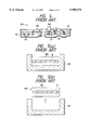
- FIG. 1 is a sectional view for explaining a mold releasing step in a method of producing the resin-coated mount substrate, as an embodiment of the present invention.
- FIG. 2 is a perspective view for explaining the step of setting a substrate unit and a bag-like body in the method of producing the resin-coated mount substrate, as the embodiment of the present invention.
- FIGS. 3(a) and 3(b) are views for explaining a sealing resin material injection step in the method of producing the resin-coated mount substrate, as the embodiment of the present invention, FIG. 3(a) being a perspective view and FIG. 3(b) being a sectional view taken along line III b --III b of FIG. 3(a).
- FIG. 4 is a sectional view showing an example of a conventional resin-coated mount substrate.
- FIGS. 5(a) and 5(b) are sectional views for explaining a method of producing another example of a conventional resin-coated mount substrate, FIG. 5(a) showing a state where a sealing resin material has been injected, and FIG. 5(b) showing the state of mold releasing.
- FIG. 1 shows a resin-coated mount substrate 1 which is an embodiment of the present invention.
- a substrate unit A is constituted by a printed substrate 2 on which electronic parts such as a relay block 3 is mounted. At least conductor portions of the printed substrate 2 and relay block 3 are buried in a sealing resin material 6 in a bag-like body 5 of a thin resin film set in an injection mold 7, and the sealing resin material 6 is then hardened and released from the injection mold 7 together with the bag-like body 5.
- the conductor portions include circuit conductors (not shown) printed on the printed substrate 2 and terminals 4 of the relay block 3 connected to the circuit conductors.
- the whole of the printed substrate 2 including the conductor portions is buried in the hardened sealing resin material 6.
- the bag-like body 5 covers that outside surface of the hardened sealing resin material 6 except its upper surface and integrally stuck on the outside surface.
- the thin-resin film bag-like body 5 formed so as to be fit to the mold shape of the injection mold 7 is set into the injection mold 7.
- the injection mold 7 is molded like a tray with a rectangular opening portion having an area substantially corresponding to the plane area of the printed substrate 2, and seat portions 7a formed at four corners of a bottom portion 7b of the injection mold 7 so as to project therefrom for mounting the printed substrate 2 thereon.
- the bag-like body 5, on the other hand, is shaped, for example, vacuum shaped by using a thin resin film (the thickness is 0.5 mm or less) such as polyethylene, polypropylene, polystyrene, or the like.
- the bag-like body 5 is formed into a tray-like shape so as to fit to the mold shape of the injection mold 7 in a manner so that recess portions 5a each having a caved lower surface and a projected upper surface are formed at four corners of a bottom portion 5b of the bag-like body 5 so that the recess portions 5a can be mounted on the respective seat portions 7a of the injection mold 7 from above.
- a circumferential wall 5c of the bag-like body 5 is formed so as to be lower in height than a circumferential wall 7c of the injection mold 7.
- the bag-like body 5 is set in the injection mold 7 in a manner so that the recess portions 5a are fitted respectively onto the seat portions 7a, and the bottom portion 5b and circumferential wall 5c are made to be in contact with the bottom portion 7b and the circumferential wall 7c respectively.
- the bag-like body 5 can keep its tray-like shape at the time of resin injection notwithstanding the fact that it is difficult to keep the shape of the bag-like body 5 because it is formed of a thin resin film.
- the substrate unit A having the relay block 3 mounted on the printed substrate 2 is set in the bag-like body 5 set in the foregoing step.
- the setting of the substrate unit A is performed by making the four corners of the lower surface of the printed substrate 2 abut and mount on the upper surfaces of the recess portions 5a of the bag-like body 5.
- the printed substrate 2 is set so as to be separated up from the bottom portion 5b of the bag-like body 5 so that it is possible to secure a resin material injection space between the printed substrate 2 and the bottom portion 5b of the bag-like body 5.
- the melted sealing resin material 6 is injected into the bag-like body 5 so that, with respect to the substrate unit A set in the foregoing step, at least the printed circuit conductors (not shown) of the printed substrate 2 and the terminals 4 of the relay block 3 are buried in the sealing resin material 6.
- Injection holes 2a and 3a are bored through the printed substrate 2 and the relay block 3 respectively.
- a nozzle 8a of a dispenser 8 is passed through the injection holes 2a and 3a (see FIG. 3(b)) and the melted sealing resin material 6 is injected through the nozzle 8a.
- the sealing resin material 6 for example, urethane resin or epoxy resin is used.
- the injection of the sealing resin material 6 is limited to such a quantity that at least the respective printed circuit conductors and terminals 4 of the printed substrate 2 and relay block 3, respectively, of the substrate unit A can be buried (see FIG. 3(b)) in the sealing resin material to thereby prevent the weight from increasing due to excessive injection.
- the sealing resin material 6 is released from the injection mold 7 together with the bag-like body 5 (see FIG. 1).
- the mold releasing is performed by grasping both the relay block 3 and the injection mold 7 and separating them from each other, because the relay block 3 is projected out from the injection mold 7.
- the mold releasing at this time can be easily performed in the state where no stress is applied onto the printed substrate 2 because the bag-like body 5 is interposed between the hardened sealing resin material 6 and the injection mold 7 so that the sealing resin material 6 does not adhere to the injection mold 7.
- the resin-coated mount substrate 1 can be produced.
- the resin-coated mount substrate 1 is accommodated, as it is, into an exterior casing (not shown) for practical use.
- This state of use can be made light in weight and compact in size because the bag-like body 5 is formed of a thin resin film. Accordingly, the weight is not increased and the size of the exterior casing is not enlarged.
- mold releasing can be easily performed with no stress applied onto the printed substrate 2 because the mold releasing is carried out in a state such that the bag-like body 5 is interposed between the hardened sealing resin material 6 and the injection mold 7.
- the substrate 1 can be easily produced with high reliability so that no damage or the like is generated in the printed circuit conductors of the printed substrate 2 and the terminals 4 of the relay block 3 at the time of mold releasing.
- mold releasing can be easily performed without any trouble. Accordingly, the resin-coated mount substrate 1 having the foregoing effects can be produced under excellent workability.
- the mold releasing step in the producing method according to the present invention may be performed as follows.
- mold releasing of the resin-coated mount substrate in which the electronic parts are almost or perfectly buried in the sealing resin material is performed in such a manner that the circumferential wall 5c of the bag-like body 5 is made sufficiently higher in height than the circumferential wall 7c of the injection mold 7 so that the mold releasing is performed by grasping both a projection portion 5d (see FIG. 3(b)) of the circumferential wall 5c projected up from the circumferential wall 7c and the injection mold 7 and separating the two from each other.
- the bag-like body after mold releasing is integrally stuck on the outside surface of the hardened sealing resin material and accommodated, as it is, in the exterior casing for practical use.
- the state of use can be made light in weight and compact in size because the bag-like body is formed of a thin resin film. Accordingly, the weight of the whole is not heavy and the size of the exterior casing is not large.
- mold releasing can be easily performed with no stress applied onto the printed substrate because the bag-like body is interposed between the hardened sealing resin material and the injection mold at the time of mold releasing.
- a resin-coated mount substrate which can be easily produced with high reliability so that no damage or the like is generated in the conductor portions of the printed substrate and the electronic parts at the time of mold releasing.
- mold releasing of the hardened sealing resin material can be easily performed with no stress applied onto the printed substrate because the mold releasing is carried out in such a state that the bag-like body is interposed between the sealing resin material and the injection mold. Moreover, since the bag-like body is formed of a thin resin film, it is possible to produce the foregoing resin-coated mount substrate of the first aspect under excellent workability.
Abstract
A substrate unit is constituted by a printed substrate on which electronic parts such as a relay block is mounted, and at least printed circuit conductors and terminals in the printed substrate and relay block are buried in a sealing resin material hardened in a bag-like body of a thin resin film set in an injection mold, and the hardened sealing resin material is then released from the injection mold together with the bag-like body.
Description
The present invention relates to a resin-coated mount substrate constituting, for example, an electronic circuit of an electronic controller mounted on a car, and relates to a method of producing such a resin-coated mount substrate.
A resin-coated mount substrate is configured such that a substrate unit in which various electronic parts are mounted on a printed substrate is resin-coated with a sealing resin material for the purpose of performing waterproof, moisture-proof, corrosion-proof, and/or heat release, etc.
Conventionally, such a resin-coated mount substrate is produced by the following method.
A resin-coated mount substrate 100 shown in FIG. 4 is disclosed in Japanese Patent Unexamined Publication No. Sho. 60-54457. The substrate 100 is formed in such a manner that electronic parts such as a resistance 102, a transistor 103, and a microcomputer 104 are mounted on a printed substrate 101 to constitute a substrate unit A, the substrate unit A is attached in a casing 110, and then a sealing resin material 111 is injected into the casing 110 and hardened so that the substrate unit A is buried in the sealing resin material 111. The resin-coated mount substrate 100 is used as it is in the state where the hardened sealing resin material 111 and the casing 110 are integrally formed with each other, and the casing 110 is used as an exterior casing as it is.
Alternatively, the resin-coated mount substrate 100 may be formed by using a tray-like casing for injecting sealing resin in place of the casing 110 used as an exterior casing. In this case, a tray-like casing and a sealing resin material are integrated with each other and the thus obtained integrated member is accommodated in a further separately prepared exterior casing for practical use.
Various techniques similar to the resin-coated mount substrate 100 are disclosed in Japanese Patent Unexamined Publications No. Sho. 59-112700 and No. Sho. 60-17990; Japanese Utility Model Unexamined Publications No. Sho. 60-11475, No. Sho. 60-94882, and No. Sho. 61-134082; etc.
Further, a resin-coated mount substrate 200 shown in FIGS. 5(a) and 5(b) is formed in such a manner that a substrate unit B in which various electronic parts (not shown) are mounted on a printed substrate is set into an injection mold 201, and thereafter a sealing resin material 202 is injected into the injection mold 201 and hardened so that the substrate unit B is buried in the sealing resin material 202 (see FIG. 5(a)), and then the hardened sealing resin material 202 is released from the mold 201 (see FIG. 5(b)). The resin-coated mount substrate 200 is accommodated in a further separately prepared exterior casing for practical use.
One problem with the resin-coated mount substrate 100, however, is that when the casing 110 is used as an exterior casing, a large the quantity of the sealing resin material 111 must be injected into the casing 110 increasing the weight. Additionally, in the case of performing molding by using a tray-like casing for injecting sealing resin, the exterior casing is increased in size to secure a space for accommodating the tray-like casing.
The resin-coated mount substrate 200 can solve the foregoing problem with the resin-coated mount substrate 100. The substrate 200, however, has a problem with adhesion between the sealing resin material 202 and the injection mold 201, even in the case where a mold releasing agent is applied. This adhesion makes mold releasing troublesome and there are concerns that stress applied to the substrate at the time of mold releasing will generate a crack in the substrate or damage the conductor portions. As a result, the workability and reliability is poor.
Therefore, an object of the present invention is to provide a resin-coated mount substrate in which the exterior casing is not increased in weight as well as size and which is produced easily with high reliability, and to provide a method of producing such a resin-coated mount substrate.
In order to achieve the above object, according to a first aspect of the invention, a resin-coated mount substrate is characterized in that, in a substrate unit constituted by a printed substrate on which various electronic parts are mounted, at least conductor portions of the printed substrate and the electronic parts are buried in a sealing resin material which is hardened in a bag-like body made of a thin resin film set in an injection mold, and the hardened sealing resin material is released from the injection mold together with the bag-like body.
Therefore, according to the invention of the first aspect, the sealing resin material which is hardened so that at least the conductor portions of the printed substrate and electronic parts of the substrate unit are buried therein is released from the mold together with the bag-like body. The mold releasing at this time can be easily performed in the state where no stress is applied onto the substrate because the bag-like body is interposed between the hardened sealing resin material and the injection mold.
Further, after mold releasing, the bag-like body is in a state that it is integrally stuck on an outside surface of the hardened sealing resin material so that the bag-like body is accommodated as it is in an exterior casing for practical use. Because the bag-like body is formed of a thin resin film, the exterior casing in this case can be made compact without increasing its size.
Further, according to a second aspect of the invention, a method of producing a resin-coated mount substrate is characterized by comprising the steps of: preparing a bag-like body of a thin resin film by shaping in accordance with a mold shape of an injection mold; setting the bag-like body into the injection mold; setting a substrate unit into the bag-like body, the substrate unit having various electronic parts mounted on a printed substrate; injecting a melted sealing resin material into the bag-like body so that at least conductor portions of the printed substrate and the electronic parts of the substrate unit are buried in the sealing resin material; and releasing the hardened sealing resin material together with the bag-like body from the mold.
Therefore, according to the invention of the second aspect, the bag-like body is set in the injection mold because the bag-like body is formed of a thin resin film so that the bag-like body cannot keep its vessel-like shape by itself at the time of injection of resin. The substrate unit is set in the bag-like body which has been set, and then, the melted sealing resin material is injected into the bag-like body. At this time, the injection of the sealing resin material is limited to a quantity so that at least the conductor portions of the printed substrate and electronic parts of the substrate unit can be buried in the sealing resin material to thereby prevent the weight from increasing by excessive injection. Then, the sealing resin material is hardened so that at least the conductor portions of the printed substrate and electronic parts of the substrate unit are buried in the sealing resin material, and the hardened sealing resin material is released from the mold together with the bag-like body.
The mold releasing at this time can be easily performed, because the bag-like body is interposed between the hardened sealing resin material and the injection mold so that the sealing resin material does not adhere to the injection mold and no stress is applied onto the substrate.
FIG. 1 is a sectional view for explaining a mold releasing step in a method of producing the resin-coated mount substrate, as an embodiment of the present invention.
FIG. 2 is a perspective view for explaining the step of setting a substrate unit and a bag-like body in the method of producing the resin-coated mount substrate, as the embodiment of the present invention.
FIGS. 3(a) and 3(b) are views for explaining a sealing resin material injection step in the method of producing the resin-coated mount substrate, as the embodiment of the present invention, FIG. 3(a) being a perspective view and FIG. 3(b) being a sectional view taken along line IIIb --IIIb of FIG. 3(a).
FIG. 4 is a sectional view showing an example of a conventional resin-coated mount substrate.
FIGS. 5(a) and 5(b) are sectional views for explaining a method of producing another example of a conventional resin-coated mount substrate, FIG. 5(a) showing a state where a sealing resin material has been injected, and FIG. 5(b) showing the state of mold releasing.
A preferred embodiment of the present invention will be described below with reference to the accompanied drawings.
FIG. 1 shows a resin-coated mount substrate 1 which is an embodiment of the present invention.
In the resin-coated mount substrate 1, a substrate unit A is constituted by a printed substrate 2 on which electronic parts such as a relay block 3 is mounted. At least conductor portions of the printed substrate 2 and relay block 3 are buried in a sealing resin material 6 in a bag-like body 5 of a thin resin film set in an injection mold 7, and the sealing resin material 6 is then hardened and released from the injection mold 7 together with the bag-like body 5.
In this case, the conductor portions include circuit conductors (not shown) printed on the printed substrate 2 and terminals 4 of the relay block 3 connected to the circuit conductors. The whole of the printed substrate 2 including the conductor portions is buried in the hardened sealing resin material 6. The bag-like body 5 covers that outside surface of the hardened sealing resin material 6 except its upper surface and integrally stuck on the outside surface.
Next, a method of producing the resin-coated mount substrate 1 will be described with reference to FIGS. 2 and 3.
First, the thin-resin film bag-like body 5 formed so as to be fit to the mold shape of the injection mold 7 is set into the injection mold 7. The injection mold 7 is molded like a tray with a rectangular opening portion having an area substantially corresponding to the plane area of the printed substrate 2, and seat portions 7a formed at four corners of a bottom portion 7b of the injection mold 7 so as to project therefrom for mounting the printed substrate 2 thereon. The bag-like body 5, on the other hand, is shaped, for example, vacuum shaped by using a thin resin film (the thickness is 0.5 mm or less) such as polyethylene, polypropylene, polystyrene, or the like. The bag-like body 5 is formed into a tray-like shape so as to fit to the mold shape of the injection mold 7 in a manner so that recess portions 5a each having a caved lower surface and a projected upper surface are formed at four corners of a bottom portion 5b of the bag-like body 5 so that the recess portions 5a can be mounted on the respective seat portions 7a of the injection mold 7 from above. In this embodiment, a circumferential wall 5c of the bag-like body 5 is formed so as to be lower in height than a circumferential wall 7c of the injection mold 7. The bag-like body 5 is set in the injection mold 7 in a manner so that the recess portions 5a are fitted respectively onto the seat portions 7a, and the bottom portion 5b and circumferential wall 5c are made to be in contact with the bottom portion 7b and the circumferential wall 7c respectively. By the setting, the bag-like body 5 can keep its tray-like shape at the time of resin injection notwithstanding the fact that it is difficult to keep the shape of the bag-like body 5 because it is formed of a thin resin film.
Next, the substrate unit A having the relay block 3 mounted on the printed substrate 2 is set in the bag-like body 5 set in the foregoing step. The setting of the substrate unit A is performed by making the four corners of the lower surface of the printed substrate 2 abut and mount on the upper surfaces of the recess portions 5a of the bag-like body 5. By the setting, the printed substrate 2 is set so as to be separated up from the bottom portion 5b of the bag-like body 5 so that it is possible to secure a resin material injection space between the printed substrate 2 and the bottom portion 5b of the bag-like body 5.
Next, the melted sealing resin material 6 is injected into the bag-like body 5 so that, with respect to the substrate unit A set in the foregoing step, at least the printed circuit conductors (not shown) of the printed substrate 2 and the terminals 4 of the relay block 3 are buried in the sealing resin material 6. Injection holes 2a and 3a are bored through the printed substrate 2 and the relay block 3 respectively. A nozzle 8a of a dispenser 8 is passed through the injection holes 2a and 3a (see FIG. 3(b)) and the melted sealing resin material 6 is injected through the nozzle 8a. As the sealing resin material 6, for example, urethane resin or epoxy resin is used. At this time, the injection of the sealing resin material 6 is limited to such a quantity that at least the respective printed circuit conductors and terminals 4 of the printed substrate 2 and relay block 3, respectively, of the substrate unit A can be buried (see FIG. 3(b)) in the sealing resin material to thereby prevent the weight from increasing due to excessive injection.
Next, after the sealing resin material 6 injected in the foregoing step is hardened, the sealing resin material 6 is released from the injection mold 7 together with the bag-like body 5 (see FIG. 1). In this embodiment of the present invention, the mold releasing is performed by grasping both the relay block 3 and the injection mold 7 and separating them from each other, because the relay block 3 is projected out from the injection mold 7. The mold releasing at this time can be easily performed in the state where no stress is applied onto the printed substrate 2 because the bag-like body 5 is interposed between the hardened sealing resin material 6 and the injection mold 7 so that the sealing resin material 6 does not adhere to the injection mold 7. By the mold releasing, the resin-coated mount substrate 1 can be produced.
In the state after mold releasing where the bag-like body 5 is integrally stuck on the outside surface of the hardened sealing resin material 6, the resin-coated mount substrate 1 is accommodated, as it is, into an exterior casing (not shown) for practical use. This state of use can be made light in weight and compact in size because the bag-like body 5 is formed of a thin resin film. Accordingly, the weight is not increased and the size of the exterior casing is not enlarged.
Further, in the resin-coated mount substrate 1, mold releasing can be easily performed with no stress applied onto the printed substrate 2 because the mold releasing is carried out in a state such that the bag-like body 5 is interposed between the hardened sealing resin material 6 and the injection mold 7. As a result, the substrate 1 can be easily produced with high reliability so that no damage or the like is generated in the printed circuit conductors of the printed substrate 2 and the terminals 4 of the relay block 3 at the time of mold releasing.
Moreover, in the producing method, mold releasing can be easily performed without any trouble. Accordingly, the resin-coated mount substrate 1 having the foregoing effects can be produced under excellent workability.
Alternatively, the mold releasing step in the producing method according to the present invention may be performed as follows.
That is, mold releasing of the resin-coated mount substrate in which the electronic parts are almost or perfectly buried in the sealing resin material is performed in such a manner that the circumferential wall 5c of the bag-like body 5 is made sufficiently higher in height than the circumferential wall 7c of the injection mold 7 so that the mold releasing is performed by grasping both a projection portion 5d (see FIG. 3(b)) of the circumferential wall 5c projected up from the circumferential wall 7c and the injection mold 7 and separating the two from each other.
As described above in detail, according to the present invention, the following effects can be obtained.
That is, according to the present invention of the first aspect, the bag-like body after mold releasing is integrally stuck on the outside surface of the hardened sealing resin material and accommodated, as it is, in the exterior casing for practical use. The state of use can be made light in weight and compact in size because the bag-like body is formed of a thin resin film. Accordingly, the weight of the whole is not heavy and the size of the exterior casing is not large.
Further, according to the present invention of the first aspect, mold releasing can be easily performed with no stress applied onto the printed substrate because the bag-like body is interposed between the hardened sealing resin material and the injection mold at the time of mold releasing. As a result, it is possible to provide a resin-coated mount substrate which can be easily produced with high reliability so that no damage or the like is generated in the conductor portions of the printed substrate and the electronic parts at the time of mold releasing.
Further, according to the present invention of the second aspect, mold releasing of the hardened sealing resin material can be easily performed with no stress applied onto the printed substrate because the mold releasing is carried out in such a state that the bag-like body is interposed between the sealing resin material and the injection mold. Moreover, since the bag-like body is formed of a thin resin film, it is possible to produce the foregoing resin-coated mount substrate of the first aspect under excellent workability.
Claims (5)
1. A resin-coated mount substrate, comprising:
a bag-like body made of a thin resin film;
a sealing resin material hardened in said bag-like body and fixed to an inside of said bag-like body; and
a printed substrate on which an electronic part is mounted, wherein conductor portions of said printed substrate and said electronic part are embedded in said sealing resin material.
2. A method of producing a resin-coated mount substrate, comprising the steps of:
preparing a bag-like body of a thin resin film by shaping said bag-like body to substantially conform with a mold shape of an injection mold;
setting said bag-like body into said injection mold;
setting a substrate unit into said bag-like body, said substrate unit including a printed substrate and an electronic part mounted on said printed substrate;
injecting a melted sealing resin material into said bag-like body so that conductor portions of said printed substrate and said electronic part of said substrate unit are embedded in said sealing resin material;
hardening said sealing resin material; and
releasing said hardened sealing resin material together with said bag-like body from said injection mold.
3. A resin-coated mount substrate as claimed in claim 1, wherein said bag-like body is rectangular in shape and includes an open top surface that receives said printed substrate.
4. A resin-coated mount substrate as claimed in claim 3, wherein said bag-like body further comprises recess portions in at least two corners of said bag-like body, said two corners being located at opposite sides of an axis bisecting parallel sides of said bag-like body.
5. A resin-coated mount substrate, comprising:
a body having a perimetrical side and a bottom surface, defining at least one of an interior space and an opening on a top surface, said body being made from a thin resin film;
a substrate on which at least one electronic part is mounted, wherein a surface of said substrate including conductor portions of said printed substrate and said electronic part is disposed within said interior space of said body; and
a sealing resin material fixing said substrate to said body, wherein said sealing resin encapsulates said conductor portions of said printed substrate and said electronic part.
Applications Claiming Priority (2)
| Application Number | Priority Date | Filing Date | Title |
|---|---|---|---|
| JP11148397A JP3300254B2 (en) | 1997-04-28 | 1997-04-28 | Resin-coated mounting board and method of manufacturing the same |
| JP9-111483 | 1997-04-28 |
Publications (1)
| Publication Number | Publication Date |
|---|---|
| US5995374A true US5995374A (en) | 1999-11-30 |
Family
ID=14562413
Family Applications (1)
| Application Number | Title | Priority Date | Filing Date |
|---|---|---|---|
| US09/064,605 Expired - Fee Related US5995374A (en) | 1997-04-28 | 1998-04-23 | Resin-coated mount substrate and method of producing the same |
Country Status (3)
| Country | Link |
|---|---|
| US (1) | US5995374A (en) |
| JP (1) | JP3300254B2 (en) |
| DE (1) | DE19818452B4 (en) |
Cited By (8)
| Publication number | Priority date | Publication date | Assignee | Title |
|---|---|---|---|---|
| US6650024B2 (en) | 2000-08-02 | 2003-11-18 | Autonetworks Technologies, Ltd | Vehicle power distributor and method of producing the same |
| US6665192B2 (en) * | 1997-02-18 | 2003-12-16 | Koninklijke Philips Electronics N.V. | Synthetic resin capping layer on a printed circuit |
| US20040141292A1 (en) * | 2000-03-21 | 2004-07-22 | Autonetworks Technologies, Ltd. | Power distributor for a vehicle and production method thereof |
| US20090059498A1 (en) * | 2007-09-03 | 2009-03-05 | Samsung Electronics Co., Ltd. | Electronic appliance and method for manufacturing the same |
| US20120184142A1 (en) * | 2009-10-05 | 2012-07-19 | Yazaki Corporation | Connector |
| US20130081845A1 (en) * | 2011-09-30 | 2013-04-04 | Edward Siahaan | Housing for electronic components |
| US8674558B2 (en) | 2001-10-22 | 2014-03-18 | Apple Inc. | Power adapters for powering and/or charging peripheral devices |
| US9345139B2 (en) | 2007-06-28 | 2016-05-17 | Robert Bosch Gmbh | Control module for a transmission control installed in an automatic transmission |
Families Citing this family (2)
| Publication number | Priority date | Publication date | Assignee | Title |
|---|---|---|---|---|
| JP4505364B2 (en) * | 2005-03-30 | 2010-07-21 | 本田技研工業株式会社 | Resin-sealed electric circuit device, manufacturing method thereof, and resin injection device |
| CN105163517B (en) * | 2015-08-06 | 2018-01-05 | 常州嘉诚数码科技有限公司 | FPC and conductive wire welding process |
Citations (8)
| Publication number | Priority date | Publication date | Assignee | Title |
|---|---|---|---|---|
| US3909504A (en) * | 1973-11-05 | 1975-09-30 | Carrier Tel Corp America Inc | Ruggedized package for electronic components and the like |
| US4942454A (en) * | 1987-08-05 | 1990-07-17 | Mitsubishi Denki Kabushiki Kaisha | Resin sealed semiconductor device |
| US5013900A (en) * | 1982-12-28 | 1991-05-07 | Gao Gesellschaft Fur Automation Und Organisation Mbh | Identification card with integrated circuit |
| US5051275A (en) * | 1989-11-09 | 1991-09-24 | At&T Bell Laboratories | Silicone resin electronic device encapsulant |
| US5179039A (en) * | 1988-02-05 | 1993-01-12 | Citizen Watch Co., Ltd. | Method of making a resin encapsulated pin grid array with integral heatsink |
| US5302850A (en) * | 1989-09-18 | 1994-04-12 | Seiko Epson Corporation | Semiconductor sealing mold |
| US5570272A (en) * | 1993-08-18 | 1996-10-29 | Lsi Logic Corporation | Apparatus for encapsulating an integrated circuit package |
| US5739463A (en) * | 1994-04-11 | 1998-04-14 | Raychem Corporation | Sealed electronic packaging for environmental protection of active electronics |
Family Cites Families (6)
| Publication number | Priority date | Publication date | Assignee | Title |
|---|---|---|---|---|
| JPS59112700A (en) * | 1982-12-17 | 1984-06-29 | 松下電器産業株式会社 | Waterproof device for printed board |
| JPS6017990A (en) * | 1983-07-12 | 1985-01-29 | 松下電器産業株式会社 | Method of treating waterproof of electronic circuit |
| JPS6054457A (en) * | 1983-09-02 | 1985-03-28 | Matsushita Electric Ind Co Ltd | Waterproof device of electronic controller |
| JPS61134082U (en) * | 1985-01-16 | 1986-08-21 | ||
| JPH0611475U (en) * | 1991-04-05 | 1994-02-15 | 純市 川口 | Pinch remover with lock |
| DE4224122C2 (en) * | 1992-07-22 | 1995-11-02 | Turck Werner Kg | Electronic circuit cast in a housing |
-
1997
- 1997-04-28 JP JP11148397A patent/JP3300254B2/en not_active Expired - Fee Related
-
1998
- 1998-04-23 US US09/064,605 patent/US5995374A/en not_active Expired - Fee Related
- 1998-04-24 DE DE19818452A patent/DE19818452B4/en not_active Expired - Fee Related
Patent Citations (8)
| Publication number | Priority date | Publication date | Assignee | Title |
|---|---|---|---|---|
| US3909504A (en) * | 1973-11-05 | 1975-09-30 | Carrier Tel Corp America Inc | Ruggedized package for electronic components and the like |
| US5013900A (en) * | 1982-12-28 | 1991-05-07 | Gao Gesellschaft Fur Automation Und Organisation Mbh | Identification card with integrated circuit |
| US4942454A (en) * | 1987-08-05 | 1990-07-17 | Mitsubishi Denki Kabushiki Kaisha | Resin sealed semiconductor device |
| US5179039A (en) * | 1988-02-05 | 1993-01-12 | Citizen Watch Co., Ltd. | Method of making a resin encapsulated pin grid array with integral heatsink |
| US5302850A (en) * | 1989-09-18 | 1994-04-12 | Seiko Epson Corporation | Semiconductor sealing mold |
| US5051275A (en) * | 1989-11-09 | 1991-09-24 | At&T Bell Laboratories | Silicone resin electronic device encapsulant |
| US5570272A (en) * | 1993-08-18 | 1996-10-29 | Lsi Logic Corporation | Apparatus for encapsulating an integrated circuit package |
| US5739463A (en) * | 1994-04-11 | 1998-04-14 | Raychem Corporation | Sealed electronic packaging for environmental protection of active electronics |
Cited By (11)
| Publication number | Priority date | Publication date | Assignee | Title |
|---|---|---|---|---|
| US6665192B2 (en) * | 1997-02-18 | 2003-12-16 | Koninklijke Philips Electronics N.V. | Synthetic resin capping layer on a printed circuit |
| US20040141292A1 (en) * | 2000-03-21 | 2004-07-22 | Autonetworks Technologies, Ltd. | Power distributor for a vehicle and production method thereof |
| US6650024B2 (en) | 2000-08-02 | 2003-11-18 | Autonetworks Technologies, Ltd | Vehicle power distributor and method of producing the same |
| US8674558B2 (en) | 2001-10-22 | 2014-03-18 | Apple Inc. | Power adapters for powering and/or charging peripheral devices |
| US10312704B2 (en) | 2001-10-22 | 2019-06-04 | Apple Inc. | Power adapters for powering and/or charging peripheral devices |
| US9345139B2 (en) | 2007-06-28 | 2016-05-17 | Robert Bosch Gmbh | Control module for a transmission control installed in an automatic transmission |
| US20090059498A1 (en) * | 2007-09-03 | 2009-03-05 | Samsung Electronics Co., Ltd. | Electronic appliance and method for manufacturing the same |
| CN101384140A (en) * | 2007-09-03 | 2009-03-11 | 三星电子株式会社 | Electronic appliance and method for manufacturing the same |
| US20120184142A1 (en) * | 2009-10-05 | 2012-07-19 | Yazaki Corporation | Connector |
| US8770988B2 (en) * | 2009-10-05 | 2014-07-08 | Yazaki Corporation | Connector |
| US20130081845A1 (en) * | 2011-09-30 | 2013-04-04 | Edward Siahaan | Housing for electronic components |
Also Published As
| Publication number | Publication date |
|---|---|
| DE19818452A1 (en) | 1998-10-29 |
| DE19818452B4 (en) | 2004-03-25 |
| JPH10303230A (en) | 1998-11-13 |
| JP3300254B2 (en) | 2002-07-08 |
Similar Documents
| Publication | Publication Date | Title |
|---|---|---|
| US6212755B1 (en) | Method for manufacturing insert-resin-molded product | |
| US5995374A (en) | Resin-coated mount substrate and method of producing the same | |
| JP2774906B2 (en) | Thin semiconductor device and method of manufacturing the same | |
| EP1487246B1 (en) | Resin encapsulated electronic component unit and method of manufacturing the same | |
| CA2197136A1 (en) | Plastic molding process and products produced thereby | |
| JPH0890211A (en) | Box body for electronic device, manufacturing method thereof and using method thereof | |
| EP0511014B1 (en) | Integrally molded printed circuit board and method of making the same | |
| US5853771A (en) | Molding die set and mold package | |
| JPS5824464Y2 (en) | Hybrid integrated circuit device | |
| US6735858B1 (en) | Manufacturing method for an electronic apparatus and electronic apparatus with plastic housing | |
| JPH0515445U (en) | Compound semiconductor device | |
| JPS62208696A (en) | Electronic controller housing case | |
| JP3288925B2 (en) | Electronic device and method of manufacturing the same | |
| JPH11254476A (en) | Production of resin-sealed molded product of electric/ electronic part | |
| JPH07162161A (en) | Manufacture of electronic equipment housing | |
| JP4278898B2 (en) | Electrical junction box | |
| JP3456738B2 (en) | Mold motor | |
| JP3964555B2 (en) | Waterproof structure and waterproofing method for electronic equipment | |
| JPS58121652A (en) | Hybrid integrated circuit device | |
| JPH05226851A (en) | Fixing device for electronic apparatus | |
| JPH02190398A (en) | Production of ic card | |
| JPH058107Y2 (en) | ||
| JP2793330B2 (en) | Sealed hybrid circuit device | |
| JPS5837694B2 (en) | semiconductor equipment | |
| JP3062686B2 (en) | Ground child and its forming method |
Legal Events
| Date | Code | Title | Description |
|---|---|---|---|
| AS | Assignment |
Owner name: YAZAKI CORPORATION, JAPAN Free format text: ASSIGNMENT OF ASSIGNORS INTEREST;ASSIGNORS:SUZUKI, MASATAKA;ASHIYA, HIROYUKI;MAKI, YAYOI;AND OTHERS;REEL/FRAME:009131/0038 Effective date: 19980413 |
|
| FPAY | Fee payment |
Year of fee payment: 4 |
|
| FPAY | Fee payment |
Year of fee payment: 8 |
|
| REMI | Maintenance fee reminder mailed | ||
| LAPS | Lapse for failure to pay maintenance fees | ||
| STCH | Information on status: patent discontinuation |
Free format text: PATENT EXPIRED DUE TO NONPAYMENT OF MAINTENANCE FEES UNDER 37 CFR 1.362 |
|
| FP | Lapsed due to failure to pay maintenance fee |
Effective date: 20111130 |