US5973658A - Liquid crystal display panel having a static electricity prevention circuit and a method of operating the same - Google Patents
Liquid crystal display panel having a static electricity prevention circuit and a method of operating the same Download PDFInfo
- Publication number
- US5973658A US5973658A US08/873,927 US87392797A US5973658A US 5973658 A US5973658 A US 5973658A US 87392797 A US87392797 A US 87392797A US 5973658 A US5973658 A US 5973658A
- Authority
- US
- United States
- Prior art keywords
- voltage
- gate
- input
- external terminal
- transmission
- Prior art date
- Legal status (The legal status is an assumption and is not a legal conclusion. Google has not performed a legal analysis and makes no representation as to the accuracy of the status listed.)
- Expired - Lifetime
Links
Images


Classifications
-
- G—PHYSICS
- G02—OPTICS
- G02F—OPTICAL DEVICES OR ARRANGEMENTS FOR THE CONTROL OF LIGHT BY MODIFICATION OF THE OPTICAL PROPERTIES OF THE MEDIA OF THE ELEMENTS INVOLVED THEREIN; NON-LINEAR OPTICS; FREQUENCY-CHANGING OF LIGHT; OPTICAL LOGIC ELEMENTS; OPTICAL ANALOGUE/DIGITAL CONVERTERS
- G02F1/00—Devices or arrangements for the control of the intensity, colour, phase, polarisation or direction of light arriving from an independent light source, e.g. switching, gating or modulating; Non-linear optics
- G02F1/01—Devices or arrangements for the control of the intensity, colour, phase, polarisation or direction of light arriving from an independent light source, e.g. switching, gating or modulating; Non-linear optics for the control of the intensity, phase, polarisation or colour
- G02F1/13—Devices or arrangements for the control of the intensity, colour, phase, polarisation or direction of light arriving from an independent light source, e.g. switching, gating or modulating; Non-linear optics for the control of the intensity, phase, polarisation or colour based on liquid crystals, e.g. single liquid crystal display cells
- G02F1/133—Constructional arrangements; Operation of liquid crystal cells; Circuit arrangements
- G02F1/136—Liquid crystal cells structurally associated with a semi-conducting layer or substrate, e.g. cells forming part of an integrated circuit
- G02F1/1362—Active matrix addressed cells
- G02F1/136204—Arrangements to prevent high voltage or static electricity failures
-
- G—PHYSICS
- G09—EDUCATION; CRYPTOGRAPHY; DISPLAY; ADVERTISING; SEALS
- G09G—ARRANGEMENTS OR CIRCUITS FOR CONTROL OF INDICATING DEVICES USING STATIC MEANS TO PRESENT VARIABLE INFORMATION
- G09G3/00—Control arrangements or circuits, of interest only in connection with visual indicators other than cathode-ray tubes
- G09G3/20—Control arrangements or circuits, of interest only in connection with visual indicators other than cathode-ray tubes for presentation of an assembly of a number of characters, e.g. a page, by composing the assembly by combination of individual elements arranged in a matrix no fixed position being assigned to or needed to be assigned to the individual characters or partial characters
- G09G3/34—Control arrangements or circuits, of interest only in connection with visual indicators other than cathode-ray tubes for presentation of an assembly of a number of characters, e.g. a page, by composing the assembly by combination of individual elements arranged in a matrix no fixed position being assigned to or needed to be assigned to the individual characters or partial characters by control of light from an independent source
- G09G3/36—Control arrangements or circuits, of interest only in connection with visual indicators other than cathode-ray tubes for presentation of an assembly of a number of characters, e.g. a page, by composing the assembly by combination of individual elements arranged in a matrix no fixed position being assigned to or needed to be assigned to the individual characters or partial characters by control of light from an independent source using liquid crystals
- G09G3/3611—Control of matrices with row and column drivers
- G09G3/3648—Control of matrices with row and column drivers using an active matrix
-
- G—PHYSICS
- G02—OPTICS
- G02F—OPTICAL DEVICES OR ARRANGEMENTS FOR THE CONTROL OF LIGHT BY MODIFICATION OF THE OPTICAL PROPERTIES OF THE MEDIA OF THE ELEMENTS INVOLVED THEREIN; NON-LINEAR OPTICS; FREQUENCY-CHANGING OF LIGHT; OPTICAL LOGIC ELEMENTS; OPTICAL ANALOGUE/DIGITAL CONVERTERS
- G02F2202/00—Materials and properties
- G02F2202/22—Antistatic materials or arrangements
-
- G—PHYSICS
- G09—EDUCATION; CRYPTOGRAPHY; DISPLAY; ADVERTISING; SEALS
- G09G—ARRANGEMENTS OR CIRCUITS FOR CONTROL OF INDICATING DEVICES USING STATIC MEANS TO PRESENT VARIABLE INFORMATION
- G09G2310/00—Command of the display device
- G09G2310/02—Addressing, scanning or driving the display screen or processing steps related thereto
- G09G2310/0243—Details of the generation of driving signals
- G09G2310/0248—Precharge or discharge of column electrodes before or after applying exact column voltages
-
- G—PHYSICS
- G09—EDUCATION; CRYPTOGRAPHY; DISPLAY; ADVERTISING; SEALS
- G09G—ARRANGEMENTS OR CIRCUITS FOR CONTROL OF INDICATING DEVICES USING STATIC MEANS TO PRESENT VARIABLE INFORMATION
- G09G2310/00—Command of the display device
- G09G2310/02—Addressing, scanning or driving the display screen or processing steps related thereto
- G09G2310/0243—Details of the generation of driving signals
- G09G2310/0251—Precharge or discharge of pixel before applying new pixel voltage
-
- G—PHYSICS
- G09—EDUCATION; CRYPTOGRAPHY; DISPLAY; ADVERTISING; SEALS
- G09G—ARRANGEMENTS OR CIRCUITS FOR CONTROL OF INDICATING DEVICES USING STATIC MEANS TO PRESENT VARIABLE INFORMATION
- G09G2330/00—Aspects of power supply; Aspects of display protection and defect management
- G09G2330/04—Display protection
-
- Y—GENERAL TAGGING OF NEW TECHNOLOGICAL DEVELOPMENTS; GENERAL TAGGING OF CROSS-SECTIONAL TECHNOLOGIES SPANNING OVER SEVERAL SECTIONS OF THE IPC; TECHNICAL SUBJECTS COVERED BY FORMER USPC CROSS-REFERENCE ART COLLECTIONS [XRACs] AND DIGESTS
- Y10—TECHNICAL SUBJECTS COVERED BY FORMER USPC
- Y10S—TECHNICAL SUBJECTS COVERED BY FORMER USPC CROSS-REFERENCE ART COLLECTIONS [XRACs] AND DIGESTS
- Y10S345/00—Computer graphics processing and selective visual display systems
- Y10S345/904—Display with fail/safe testing feature
Definitions
- the present invention relates to a liquid crystal panel for eliminating static electricity generated during the manufacture of the liquid crystal display, and a method of operating the same. More particularly, the present invention relates to a static electricity prevention type liquid crystal panel and a method of operating the same which allows testing of a driving circuit and a pixel section of a driving circuit integrated TFTLCD (thin film transistor liquid crystal display).
- TFTLCD thin film transistor liquid crystal display
- FIG. 1 shows a perspective view of conductive lines of a conventional liquid crystal display for illustrating the conventional method of preventing static electricity as described in Japanese laid-open patent publication 58-116573.
- a plurality of signal lines G and a plurality of data lines D cross each other to form a cell array.
- the signal lines are also known as gate lines G.
- a short conductor ST commonly connects the gate lines G and data lines D so as to maintain the voltage levels thereon at an equal electric potential and eliminate static electricity.
- the gate lines G and the data lines D are severed according to the dotted line CL.
- the cut portions of the gate and the data lines G and D are connected to separately manufactured gate driving and data driving circuits (not shown), respectively, to form the liquid crystal panel.
- FIG. 2 shows another technique for preventing static electricity as described in Japanese laid-open patent publication 63-220289.
- a reference potential line SL is provided external to the region where the gate and data lines G and D are positioned.
- the reference potential line SL has a certain electric potential value.
- the source terminals of NMOS transistors 2 are connected to the reference potential line SL, while the gate and drain terminals of the NMOS transistor 2 are connected to an associated data line D.
- the source terminals of NMOS transistors 4 are connected to the reference potential line SL, while the gate and drain terminals of the NMOS transistors 4 are connected to an associated gate line G. Therefore, the gate lines G and the data lines D are connected to the reference potential line SL through a terminal element of an NMOS transistor. Through the gate lines G and data lines D, a certain voltage generated due to static electricity is input to the NMOS transistors 2 and 4 so as to minimize malfunctions caused by the static electricity.
- An apparatus for controlling at least one transmission line in a liquid crystal display said liquid crystal display including a plurality of pixels, each pixel including a thin film transistor, at least one thin film transistor connected to said transmission line, said apparatus comprising: at least one transmission gate having first and second gates, an input and an output, said input connected to said transmission line, said transmission gate transmitting when one of a first voltage of said first gate is greater than a voltage of said input and a second voltage of said second gate is less than said voltage of said input; a first external terminal connected to said first gate; a second external terminal connected to said second gate; and a common external terminal connected to said output of said transmission gate.
- a method for controlling at least one transmission line in a liquid crystal display said liquid crystal display including a plurality of pixels, each pixel including a thin film transistor, at least one thin film transistor connected to said transmission line, said method comprising: providing at least one transmission gate having first and second gates, an input and an output, said input connected to said transmission line, said transmission gate transmitting when one of a first voltage of said first gate is greater than a voltage of said input and a second voltage of said second gate is less than said voltage of said input; first applying a first voltage to said first gate; second applying a second voltage to said second gate; and third applying a third voltage to said output.
- FIG. 1 shows a perspective view of a liquid crystal display panel for explaining a conventional method of preventing static electricity in a liquid crystal display
- FIG. 2 shows a schematic view of a circuit of a liquid crystal display panel for illustrating another conventional method of preventing static electricity in a liquid crystal display
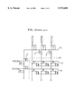
- FIG. 3 shows a view of a liquid crystal display panel which eliminates static electricity in accordance with an embodiment of the present invention
- FIG. 4. shows a graph for explaining operational characteristics of a transmission gate used in the liquid crystal display panel of the present invention
- FIG. 5 shows a view of a liquid crystal display panel which eliminates static electricity in accordance with another embodiment of the present invention.
- FIG. 6 shows a view of a liquid crystal display panel which eliminates static electricity in accordance with another embodiment of the present invention.
- the liquid crystal display panel as shown in FIG. 3 includes a plurality of data lines D and a plurality of gate lines G crossing each other to form a matrix type pixel array.
- Each pixel includes a thin film transistor 10 connected to the corresponding data line D and gate line G, and a pixel electrode 12 connected to the drain electrode of the thin film transistor (TFT) 10.
- TFT thin film transistor
- the liquid crystal display panel further includes a plurality of first and second CMOS transmission gates TG1 and TG2, each connected to a first or open end portion of a data and gate line D and G, respectively. Also, the second end portion of each gate and data line G and D is connected to a gate driving circuit and a data driving circuit, respectively.
- the first transmission gates TG1 are each formed by connecting a first NMOS transistor 14 and a first PMOS transistor 16.
- the gates of the first NMOS transistors 14 are commonly connected to a first external control terminal C1.
- the gate terminals of the first PMOS transistors 16 are commonly connected to a second external control terminal C2.
- the second transmission gates TG2 are each formed by connecting a second NMOS transistor 18 and a second PMOS transistor 20.
- the gate terminals of the second NMOS transistors 18 are commonly connected to a fourth external control terminal C4.
- the gate terminals of the second PMOS transistors 20 are commonly connected to a fifth external control terminal C5.
- the outputs of the first and second transmission gates TG1 and TG2 are commonly connected to a third external control terminal C3. Between the first and the second external control terminals C1 and C2 and between the fourth and fifth external control terminals C4 and C5, a resistor R1 having a certain resistance value is connected. If the resistance value of the resistor R1 is too large, it may minimize the effectiveness of the static electricity prevention technique according to the present invention. Therefore, it is preferable to consider the power consumption of the completed panel during operation, and use an appropriate resistance value for the resistor R1.
- the resistance of resistor R1 should be between 1 K ⁇ and 100 M ⁇ , preferably between 10 K ⁇ and 100 K ⁇ , and more preferably 50 K ⁇ .
- the first and second transmission gates TG1 and TG2 respectively include first and second NMOS transistors 14 or 18 and first and second PMOS transistors 16 or 20.
- An operation channel is formed for each of the first and second transmission gates TG1 and TG2 depending on the potential difference Vgs between the source and gate terminals, respectively, of the first and second NMOS and PMOS transistors 14, 18, 16 and 20.
- FIG. 4 shows the operation characteristics of the first and second NMOS transistors 14 and 18 and the first and second PMOS transistors 16 and 20 with respect to Vgs. As shown in FIG. 4, the first and second NMOS transistors 14 and 18 are turned on when Vgs is positive, whereas the first and second PMOS transistors 16 and 20 are turned on when Vgs is negative.
- At least one of the first NMOS and PMOS transistors 14 and 16 in each of the first transmission gates TG1 and at least one of the second NMOS and PMOS transistors 18 and 20 in each of the second transmission gates TG2 are in a conductive state.
- the operation of the first and second transmission gates TG1 and TG2 will be descried in greater detail. If the electric potential of a data line D were to increase due to static electricity the terminal of the first PMOS transistor 16 connected to the data line functions as a source. This results in a negative (-) Vgs in the first PMOS transistor 16.
- the negative Vgs turns on the first PMOS transistor 16 of the transmission gate TG1 which allows the static electricity from the data line D to be discharged.
- the first NMOS transistor 14 of the first transmission gate TG1 is turned on to discharge the static electricity therefrom. Since the second transmission gates TG2 operate in the same manner with respect to the gate lines G, that description will not be repeated for the sake of brevity.
- the respective first or second transmission gate TG1 or TG2 connected thereto is turned on to transmit the static electricity to the third external control terminal C3.
- the third external control terminal C3 By connecting the third external control terminal C3 to ground, any static electricity output from or through the first and second transmission gates TG1 and TG2 is discharged to ground through the third external control terminal C3.
- the device as shown in FIG. 3 is used to test the gate driving circuit or the data driving circuit.
- a low level signal is applied to the first external control terminal Cl and a high level signal is applied to the second external control terminal C2.
- the transmission gates TG1 connected to the data lines D are turned off. As a result, the data lines D are isolated and become available for testing.
- the second transmission gates TG2 are turned off. As a result, the gate lines G are isolated and become available for testing.
- the present invention overcomes the technical limitations of the conventional static prevention technique as shown in FIG. 1, and allows testing of driving circuits.
- the present invention can be used to pre-charge the pixels.
- a pixel when driven, a pixel is alternatively charged to a positive polarity data value +Vd and a negative polarity data value -Vd.
- a pre-charge voltage is applied to the third external control terminal C3.
- the pre-charge voltage is greater than Vd when Vd will be applied to the pixel, and is less than -Vd when -Vd will be applied to the pixel.
- a high level signal is applied to the first external control terminal Cl and a low level signal is applied to the second external control terminal C2.
- the electric potential applied to the third external terminal C3 is established at the output terminal of the first transmission gates TG1, and is, thus, established at each of the data lines D.
- the gate lines G are maintained in the isolated state.
- the isolated state is established by applying a low level signal to the fourth external control terminal C4 and applying a high level signal to the fifth external control terminal C5.
- the pre-charge operation described above involves applying a pre-charge signal to the data lines D after the gate driving signal is applied to the gate lines G, but before data signals are applied to the data lines D, so as to pre-charge the pixel electrodes. As a result, the charge time for the pixels is reduced.
- the terminal to which the pre-charge voltage is applied is the source terminal of the PMOS transistor.
- the output terminal connected to the third external control terminal C3 of the first and second transmission gates TG1 and TG2 functions as a voltage input terminal.
- the first transmission gates TG1 are turned on. Since the transmission gates TG1 function as bi-directional transmission gates, when the transmission gates TG1 are turned on and a pre-charge voltage is applied to the third external C3, the pre-charge voltage is transmitted to the data lines D for pre-charging the pixel electrodes connected to the data lines D.
- the present invention provides a pre-charge function as described above.
- FIG. 5 illustrates another embodiment of a liquid crystal display panel which eliminates static electricity according to the present invention.
- FIG. 5 is substantially the same as FIG. 3 except that the third external terminal C3 has been replaced by a sixth external terminal C6 and seventh external terminal C7 connected via a second resistor R2.
- the first transmission gates TG1 have their outputs connected to the sixth external terminal C6, while the second transmission gates TG2 have their outputs connected to the seventh external terminal C7.
- the resistance of the second resistor R2 should be chosen such that a proper voltage drop is achieved across the second resistor R2 to allow for the different voltages at the seventh external terminal C7 and the sixth external terminal C6. For example, a 100 K ⁇ resistance is proper when 20 volts is applied to the seventh terminal C7 and 5 volts is applied to the sixth terminal C6.
- FIG. 6 illustrates another embodiment of the liquid crystal display panel which eliminates static electricity in accordance with the present invention.
- FIG. 6 is substantially the same as FIG. 3, except that the third external terminal C3 has been replaced by an eighth external terminal C8 and a ninth external terminal C9 connected to one another via a third transmission gate TG3.
- the third transmission gate TG3 includes a third NMOS transistor 22 and a third PMOS transistor 24 connected to one another.
- the gate of the third NMOS transistor 22 is connected to the second external terminal C2, while the gate of the third PMOS transistor 24 is connected to the first external terminal C1.
- the third transmission gate TG3 conducts when the first and second external terminals C1 and C2 are in the floating state such that the data and gate lines are at the same potential.
- the third transmission gate TG3 is turned on connecting the eighth external terminal C8 and the ninth external terminal C9.
- the third transmission gate TG3 is turned off; thus, allowing for different potentials to be applied to the eighth external terminal C8 and the ninth external terminal C9.
- the resistor R1 connected between the first and second external control terminals C1 and C2 and between the fourth and fifth external control terminals C4 and C5, is fixed in the panel.
- such an arrangement is only an example of the present invention and one of ordinary skill in the art would be able to suggest variations as well as practical applications of the present invention.
- a resistance value of between 1 K ⁇ to 100 M ⁇ for the resistor R1 may be utilized to reduce power consumption during operation of the completed product.
- the resistor R1 can be eliminated upon completion of the manufacturing process and/or testing.
- static electricity may be eliminated during or upon completion of the manufacturing process.
Abstract
Description
Claims (40)
Applications Claiming Priority (2)
| Application Number | Priority Date | Filing Date | Title |
|---|---|---|---|
| KR19960063442 | 1996-12-10 | ||
| KR96-63442 | 1996-12-10 |
Publications (1)
| Publication Number | Publication Date |
|---|---|
| US5973658A true US5973658A (en) | 1999-10-26 |
Family
ID=19486775
Family Applications (1)
| Application Number | Title | Priority Date | Filing Date |
|---|---|---|---|
| US08/873,927 Expired - Lifetime US5973658A (en) | 1996-12-10 | 1997-06-12 | Liquid crystal display panel having a static electricity prevention circuit and a method of operating the same |
Country Status (2)
| Country | Link |
|---|---|
| US (1) | US5973658A (en) |
| KR (1) | KR100234940B1 (en) |
Cited By (29)
| Publication number | Priority date | Publication date | Assignee | Title |
|---|---|---|---|---|
| US6104449A (en) * | 1997-11-14 | 2000-08-15 | Sharp Kabushiki Kaisha | Liquid crystal display device having DTFTs connected to a short ring |
| US6266039B1 (en) * | 1997-07-14 | 2001-07-24 | Seiko Epson Corporation | Liquid crystal device, method for driving the same, and projection display and electronic equipment made using the same |
| US6304305B1 (en) * | 1997-10-20 | 2001-10-16 | Nec Corporation | Active matrix liquid crystal display |
| US20010030716A1 (en) * | 2000-04-12 | 2001-10-18 | Park Jeong Ki | Liquid crystal display |
| US6335721B1 (en) * | 1998-03-27 | 2002-01-01 | Hyundai Electronics Industries Co., Ltd. | LCD source driver |
| US6337722B1 (en) * | 1997-08-07 | 2002-01-08 | Lg.Philips Lcd Co., Ltd | Liquid crystal display panel having electrostatic discharge prevention circuitry |
| US20020105512A1 (en) * | 2000-12-06 | 2002-08-08 | Samsung Electronics Co., Ltd. | Liquid crystal device driver circuit for electrostatic discharge protection |
| US6515644B1 (en) * | 1999-09-21 | 2003-02-04 | Lg.Philips Lcd Co., Ltd. | Static electricity prevention circuit in liquid crystal display |
| WO2003014809A2 (en) * | 2001-08-08 | 2003-02-20 | Koninklijke Philips Electronics N.V. | Electrostatic discharge protection for pixellated electronic device |
| US6580594B2 (en) * | 1999-12-28 | 2003-06-17 | Stmicroelectronics S.A. | Device for the protection of interconnection lines in an integrated circuit |
| US20030189685A1 (en) * | 2002-04-08 | 2003-10-09 | Choi Seung Kyu | Liquid crystal display of line-on-glass type |
| US20030214470A1 (en) * | 2002-05-15 | 2003-11-20 | Wein-Town Sun | Pre-charging display apparatus |
| US6670940B2 (en) * | 2000-12-16 | 2003-12-30 | Samsung Electronics Co., Ltd. | Flat panel display and drive method thereof |
| US20040027502A1 (en) * | 1999-08-31 | 2004-02-12 | Fujitsu Display Technologies Corporation | Liquid crystal display |
| US6774957B2 (en) * | 1997-09-26 | 2004-08-10 | Sanyo Electric Co., Ltd. | Display apparatus having an electric shielding wire and method for manufacturing the same |
| WO2004072941A2 (en) * | 2003-02-14 | 2004-08-26 | Koninklijke Philips Electronics N.V. | Display device with electrostatic discharge protection circuitry |
| US20050200417A1 (en) * | 2002-10-08 | 2005-09-15 | Impinj, Inc., A Delaware Corporation | Use of analog-valued floating-gate transistors for parallel and serial signal processing |
| US20050243043A1 (en) * | 2004-04-30 | 2005-11-03 | Lg.Philips Lcd Co., Ltd. | Liquid crystal display and pre-charging method thereof |
| US20060145744A1 (en) * | 2002-10-08 | 2006-07-06 | Impinj, Inc. | Use of analog-valued floating-gate transistors to match the electrical characteristics of interleaved and pipelined circuits |
| US20080239613A1 (en) * | 2007-03-27 | 2008-10-02 | Prime View International Co., Ltd. | Active matrix device or a flat panel display with electrostatic protection |
| US20090051634A1 (en) * | 2007-08-21 | 2009-02-26 | Au Optronics Corporation | Liquid Crystal Display |
| US20130027074A1 (en) * | 2011-07-26 | 2013-01-31 | Shenzhen China Star Optoelectronics Technology Co., Ltd. | Voltage Test devices Used in LCD Panels and a System Thereof |
| JP2015084034A (en) * | 2013-10-25 | 2015-04-30 | 株式会社ジャパンディスプレイ | Display device |
| CN105527768A (en) * | 2016-01-25 | 2016-04-27 | 武汉华星光电技术有限公司 | Liquid crystal display device and liquid crystal display panel thereof |
| CN105976785A (en) * | 2016-07-21 | 2016-09-28 | 武汉华星光电技术有限公司 | Goa circuit and liquid crystal display panel |
| CN106597766A (en) * | 2015-10-16 | 2017-04-26 | 群创光电股份有限公司 | Display apparatus |
| JP2018081312A (en) * | 2009-09-24 | 2018-05-24 | 株式会社半導体エネルギー研究所 | Display device |
| US10964260B2 (en) * | 2018-03-09 | 2021-03-30 | Seiko Epson Corporation | Electro-optical device, driving method for electro-optical device, and electronic apparatus |
| US11238765B2 (en) * | 2020-03-16 | 2022-02-01 | Samsung Display Co., Ltd. | Display device |
Families Citing this family (3)
| Publication number | Priority date | Publication date | Assignee | Title |
|---|---|---|---|---|
| JP3718355B2 (en) * | 1998-11-26 | 2005-11-24 | 株式会社 日立ディスプレイズ | Liquid crystal display device |
| TW501069B (en) * | 1999-08-18 | 2002-09-01 | Thomson Licensing Sa | Method of operating capacitive thin film transistor arrays |
| JP5140999B2 (en) | 2006-11-22 | 2013-02-13 | カシオ計算機株式会社 | Liquid crystal display |
Citations (9)
| Publication number | Priority date | Publication date | Assignee | Title |
|---|---|---|---|---|
| JPH03220289A (en) * | 1989-11-30 | 1991-09-27 | Mitsubishi Rayon Co Ltd | Ferroelectric liquid crystal composition and optical device |
| US5068748A (en) * | 1989-10-20 | 1991-11-26 | Hosiden Corporation | Active matrix liquid crystal display device having improved electrostatic discharge protection |
| US5220443A (en) * | 1991-04-29 | 1993-06-15 | Nec Corporation | Matrix wiring substrate and active matrix display having non-linear resistance elements for electrostatic discharge protection |
| US5373377A (en) * | 1992-02-21 | 1994-12-13 | Kabushiki Kaisha Toshiba | Liquid crystal device with shorting ring and transistors for electrostatic discharge protection |
| US5497146A (en) * | 1992-06-03 | 1996-03-05 | Frontec, Incorporated | Matrix wiring substrates |
| JPH08116573A (en) * | 1994-08-26 | 1996-05-07 | Nec Corp | Cordless telephone system |
| US5576730A (en) * | 1992-04-08 | 1996-11-19 | Sharp Kabushiki Kaisha | Active matrix substrate and a method for producing the same |
| US5657139A (en) * | 1994-09-30 | 1997-08-12 | Kabushiki Kaisha Toshiba | Array substrate for a flat-display device including surge protection circuits and short circuit line or lines |
| US5671026A (en) * | 1994-03-02 | 1997-09-23 | Sharp Kabushiki Kaisha | Liquid crystal display device with TFT ESD protective devices between I/O terminals or with a short circuited alignment film |
-
1997
- 1997-06-12 US US08/873,927 patent/US5973658A/en not_active Expired - Lifetime
- 1997-08-23 KR KR1019970040382A patent/KR100234940B1/en not_active IP Right Cessation
Patent Citations (9)
| Publication number | Priority date | Publication date | Assignee | Title |
|---|---|---|---|---|
| US5068748A (en) * | 1989-10-20 | 1991-11-26 | Hosiden Corporation | Active matrix liquid crystal display device having improved electrostatic discharge protection |
| JPH03220289A (en) * | 1989-11-30 | 1991-09-27 | Mitsubishi Rayon Co Ltd | Ferroelectric liquid crystal composition and optical device |
| US5220443A (en) * | 1991-04-29 | 1993-06-15 | Nec Corporation | Matrix wiring substrate and active matrix display having non-linear resistance elements for electrostatic discharge protection |
| US5373377A (en) * | 1992-02-21 | 1994-12-13 | Kabushiki Kaisha Toshiba | Liquid crystal device with shorting ring and transistors for electrostatic discharge protection |
| US5576730A (en) * | 1992-04-08 | 1996-11-19 | Sharp Kabushiki Kaisha | Active matrix substrate and a method for producing the same |
| US5497146A (en) * | 1992-06-03 | 1996-03-05 | Frontec, Incorporated | Matrix wiring substrates |
| US5671026A (en) * | 1994-03-02 | 1997-09-23 | Sharp Kabushiki Kaisha | Liquid crystal display device with TFT ESD protective devices between I/O terminals or with a short circuited alignment film |
| JPH08116573A (en) * | 1994-08-26 | 1996-05-07 | Nec Corp | Cordless telephone system |
| US5657139A (en) * | 1994-09-30 | 1997-08-12 | Kabushiki Kaisha Toshiba | Array substrate for a flat-display device including surge protection circuits and short circuit line or lines |
Cited By (64)
| Publication number | Priority date | Publication date | Assignee | Title |
|---|---|---|---|---|
| US6266039B1 (en) * | 1997-07-14 | 2001-07-24 | Seiko Epson Corporation | Liquid crystal device, method for driving the same, and projection display and electronic equipment made using the same |
| US6493047B2 (en) * | 1997-08-07 | 2002-12-10 | Lg. Philips Lcd Co., Ltd. | Liquid crystal display panel having electrostatic discharge prevention circuitry |
| US6337722B1 (en) * | 1997-08-07 | 2002-01-08 | Lg.Philips Lcd Co., Ltd | Liquid crystal display panel having electrostatic discharge prevention circuitry |
| US6774957B2 (en) * | 1997-09-26 | 2004-08-10 | Sanyo Electric Co., Ltd. | Display apparatus having an electric shielding wire and method for manufacturing the same |
| US6304305B1 (en) * | 1997-10-20 | 2001-10-16 | Nec Corporation | Active matrix liquid crystal display |
| US6104449A (en) * | 1997-11-14 | 2000-08-15 | Sharp Kabushiki Kaisha | Liquid crystal display device having DTFTs connected to a short ring |
| US6335721B1 (en) * | 1998-03-27 | 2002-01-01 | Hyundai Electronics Industries Co., Ltd. | LCD source driver |
| US7342617B2 (en) * | 1999-08-31 | 2008-03-11 | Sharp Kabushiki Kaisha | Liquid crystal display comprising an electrostatic protection element formed between adjacent bus lines |
| US20040027502A1 (en) * | 1999-08-31 | 2004-02-12 | Fujitsu Display Technologies Corporation | Liquid crystal display |
| US6515644B1 (en) * | 1999-09-21 | 2003-02-04 | Lg.Philips Lcd Co., Ltd. | Static electricity prevention circuit in liquid crystal display |
| US6580594B2 (en) * | 1999-12-28 | 2003-06-17 | Stmicroelectronics S.A. | Device for the protection of interconnection lines in an integrated circuit |
| US20050225688A1 (en) * | 2000-04-12 | 2005-10-13 | Park Jeong K | Liquid crystal display |
| US20050225689A1 (en) * | 2000-04-12 | 2005-10-13 | Park Jeong K | Liquid crystal display |
| US7061554B2 (en) | 2000-04-12 | 2006-06-13 | Lg.Philips Lcd Co., Ltd. | Liquid crystal display |
| DE10117874B4 (en) * | 2000-04-12 | 2012-06-21 | Lg Display Co., Ltd. | liquid-crystal display |
| US6924853B2 (en) | 2000-04-12 | 2005-08-02 | Lg. Philips Lcd Co., Ltd. | Liquid crystal display with electrostatic protection |
| US6839097B2 (en) | 2000-04-12 | 2005-01-04 | Lg.Philips Lcd Co., Ltd. | Liquid crystal display with electrostatic protection circuits |
| US20040233345A1 (en) * | 2000-04-12 | 2004-11-25 | Park Jeong Ki | Liquid crystal display |
| US7224413B2 (en) | 2000-04-12 | 2007-05-29 | Lg.Philips Lcd Co., Ltd. | Liquid crystal display with electrostatic protecting circuits |
| US20010030716A1 (en) * | 2000-04-12 | 2001-10-18 | Park Jeong Ki | Liquid crystal display |
| US20020105512A1 (en) * | 2000-12-06 | 2002-08-08 | Samsung Electronics Co., Ltd. | Liquid crystal device driver circuit for electrostatic discharge protection |
| US6753836B2 (en) * | 2000-12-06 | 2004-06-22 | Samsung Electronics Co., Ltd. | Liquid crystal device driver circuit for electrostatic discharge protection |
| US20040090435A1 (en) * | 2000-12-16 | 2004-05-13 | Jong-Seon Kim | Flat panel display and drive method thereof |
| US6670940B2 (en) * | 2000-12-16 | 2003-12-30 | Samsung Electronics Co., Ltd. | Flat panel display and drive method thereof |
| US7133016B2 (en) | 2000-12-16 | 2006-11-07 | Samsung Electronics Co., Ltd. | Flat panel display and drive method thereof |
| KR100831344B1 (en) | 2001-08-08 | 2008-05-22 | 티피오 홍콩 홀딩 리미티드 | Electronic device |
| US6696701B2 (en) | 2001-08-08 | 2004-02-24 | Koninklijke Philips Electronics N.V. | Electrostatic discharge protection for pixellated electronic device |
| WO2003014809A3 (en) * | 2001-08-08 | 2003-06-05 | Koninkl Philips Electronics Nv | Electrostatic discharge protection for pixellated electronic device |
| WO2003014809A2 (en) * | 2001-08-08 | 2003-02-20 | Koninklijke Philips Electronics N.V. | Electrostatic discharge protection for pixellated electronic device |
| US7643121B2 (en) * | 2002-04-08 | 2010-01-05 | Lg Display Co., Ltd. | Liquid crystal display of line-on-glass type |
| US20030189685A1 (en) * | 2002-04-08 | 2003-10-09 | Choi Seung Kyu | Liquid crystal display of line-on-glass type |
| US6778158B2 (en) * | 2002-05-15 | 2004-08-17 | Au Optronics Corporation | Pre-charging display apparatus |
| US20030214470A1 (en) * | 2002-05-15 | 2003-11-20 | Wein-Town Sun | Pre-charging display apparatus |
| US20050200402A1 (en) * | 2002-10-08 | 2005-09-15 | Impinj, Inc., A Delaware Corporation | Use of analog-valued floating-gate transistors for parallel and serial signal processing |
| US7061324B2 (en) | 2002-10-08 | 2006-06-13 | Impinj, Inc. | Use of analog-valued floating-gate transistors for parallel and serial signal processing |
| US20060145744A1 (en) * | 2002-10-08 | 2006-07-06 | Impinj, Inc. | Use of analog-valued floating-gate transistors to match the electrical characteristics of interleaved and pipelined circuits |
| US20060186960A1 (en) * | 2002-10-08 | 2006-08-24 | Impinj, Inc. | Use of analog-valued floating-gate transistors for parallel and serial signal processing |
| US20050200417A1 (en) * | 2002-10-08 | 2005-09-15 | Impinj, Inc., A Delaware Corporation | Use of analog-valued floating-gate transistors for parallel and serial signal processing |
| US7187237B1 (en) | 2002-10-08 | 2007-03-06 | Impinj, Inc. | Use of analog-valued floating-gate transistors for parallel and serial signal processing |
| US7199663B2 (en) | 2002-10-08 | 2007-04-03 | Impinj, Inc. | Use of analog-valued floating-gate transistors for parallel and serial signal processing |
| US7389101B2 (en) | 2002-10-08 | 2008-06-17 | Impinj, Inc. | Use of analog-valued floating-gate transistors for parallel and serial signal processing |
| US20060145951A1 (en) * | 2003-02-14 | 2006-07-06 | Koninklijke Philips Electronics, N.V. | Display device with electrostatic discharge protection circuitry |
| WO2004072941A2 (en) * | 2003-02-14 | 2004-08-26 | Koninklijke Philips Electronics N.V. | Display device with electrostatic discharge protection circuitry |
| WO2004072941A3 (en) * | 2003-02-14 | 2004-11-11 | Koninkl Philips Electronics Nv | Display device with electrostatic discharge protection circuitry |
| US7453420B2 (en) | 2003-02-14 | 2008-11-18 | Tpo Hong Kong Holding Limited | Display device with electrostatic discharge protection circuitry |
| US7502008B2 (en) | 2004-04-30 | 2009-03-10 | Lg Display Co., Ltd. | Liquid crystal display and pre-charging method thereof |
| US20090135122A1 (en) * | 2004-04-30 | 2009-05-28 | Hun Jeoung | Liquid crystal display and pre-charging method thereof |
| US8269709B2 (en) | 2004-04-30 | 2012-09-18 | Lg Display Co., Ltd. | Liquid crystal display and pre-charging method thereof |
| US20050243043A1 (en) * | 2004-04-30 | 2005-11-03 | Lg.Philips Lcd Co., Ltd. | Liquid crystal display and pre-charging method thereof |
| US20080239613A1 (en) * | 2007-03-27 | 2008-10-02 | Prime View International Co., Ltd. | Active matrix device or a flat panel display with electrostatic protection |
| US20090051634A1 (en) * | 2007-08-21 | 2009-02-26 | Au Optronics Corporation | Liquid Crystal Display |
| US8593383B2 (en) | 2007-08-21 | 2013-11-26 | Au Optronics Corporation | Liquid crystal display with precharge circuit |
| JP2018081312A (en) * | 2009-09-24 | 2018-05-24 | 株式会社半導体エネルギー研究所 | Display device |
| US10181481B2 (en) | 2009-09-24 | 2019-01-15 | Semiconductor Energy Laboratory Co., Ltd. | Display device |
| US20130027074A1 (en) * | 2011-07-26 | 2013-01-31 | Shenzhen China Star Optoelectronics Technology Co., Ltd. | Voltage Test devices Used in LCD Panels and a System Thereof |
| US8836364B2 (en) * | 2011-07-26 | 2014-09-16 | Shenzhen China Star Optoelectronics Technology Co., Ltd | Voltage test devices used in LCD panels and a system thereof |
| JP2015084034A (en) * | 2013-10-25 | 2015-04-30 | 株式会社ジャパンディスプレイ | Display device |
| CN106597766A (en) * | 2015-10-16 | 2017-04-26 | 群创光电股份有限公司 | Display apparatus |
| US20170212374A1 (en) * | 2016-01-25 | 2017-07-27 | Wuhan China Star Optoelectronics Technology Co., Ltd. | Liquid crystal devices and the liquid crystal panels thereof |
| CN105527768A (en) * | 2016-01-25 | 2016-04-27 | 武汉华星光电技术有限公司 | Liquid crystal display device and liquid crystal display panel thereof |
| CN105976785A (en) * | 2016-07-21 | 2016-09-28 | 武汉华星光电技术有限公司 | Goa circuit and liquid crystal display panel |
| US10446094B2 (en) | 2016-07-21 | 2019-10-15 | Wuhan China Star Optoelectronics Technology Co., Ltd. | Gate driver on array circuit and LCD panel having GOA protecting circuit |
| US10964260B2 (en) * | 2018-03-09 | 2021-03-30 | Seiko Epson Corporation | Electro-optical device, driving method for electro-optical device, and electronic apparatus |
| US11238765B2 (en) * | 2020-03-16 | 2022-02-01 | Samsung Display Co., Ltd. | Display device |
Also Published As
| Publication number | Publication date |
|---|---|
| KR100234940B1 (en) | 1999-12-15 |
| KR19980063421A (en) | 1998-10-07 |
Similar Documents
| Publication | Publication Date | Title |
|---|---|---|
| US5973658A (en) | Liquid crystal display panel having a static electricity prevention circuit and a method of operating the same | |
| US6337722B1 (en) | Liquid crystal display panel having electrostatic discharge prevention circuitry | |
| KR100206567B1 (en) | Screen erase circuit and its driving method of tft | |
| KR100405026B1 (en) | Liquid Crystal Display | |
| US7116302B2 (en) | Process of operating active matrix display device having thin film transistors | |
| CN101467098B (en) | Active matrix substrate and display device having the same | |
| KR100455014B1 (en) | Bi-directional shift register | |
| US5497146A (en) | Matrix wiring substrates | |
| US5606340A (en) | Thin film transistor protection circuit | |
| KR100216489B1 (en) | Shift register useful as a selection line scanner for liquid crystal display | |
| KR0154832B1 (en) | Liquid crystal display device | |
| US8183570B2 (en) | Thin film transistor array panel | |
| JP2000356978A (en) | Data line driving method and liquid crystal display device using the method | |
| KR100628937B1 (en) | Active matrix liquid crystal display devices | |
| CN107103888B (en) | Time sequence driving circuit, driving circuit and the liquid crystal display panel of liquid crystal display panel | |
| EP0731442B1 (en) | Signal disturbance reduction arrangement for a liquid crystal display | |
| EP1381015B1 (en) | Electro-optical device, drive device and drive method for electro-optical device, and electronic apparatus | |
| US7649398B2 (en) | Level shifter with single input and liquid crystal display device using the same | |
| US7071910B1 (en) | Electrooptical device and method of driving and manufacturing the same | |
| JPH07235844A (en) | Output buffer circuit for analog driver ic | |
| US7573455B2 (en) | Analog buffer and method for driving the same | |
| CN100483241C (en) | Liquid crystal display devic,e grid driving circuit and its driving circuit unit | |
| KR100451380B1 (en) | Antistatic Liquid Crystal Display Panel | |
| KR100640047B1 (en) | Liquid Crystal Display Device | |
| CN114627836B (en) | Display panel and display device |
Legal Events
| Date | Code | Title | Description |
|---|---|---|---|
| AS | Assignment |
Owner name: LG ELECTRONICS INC., KOREA, REPUBLIC OF Free format text: ASSIGNMENT OF ASSIGNORS INTEREST;ASSIGNORS:KIM, SEONG-GYUN;YEO, JU-CHEON;REEL/FRAME:008646/0594 Effective date: 19970517 |
|
| AS | Assignment |
Owner name: LG. PHILIPS LCD CO., LTD., KOREA, DEMOCRATIC PEOPL Free format text: ASSIGNMENT OF ASSIGNORS INTEREST;ASSIGNOR:LG ELECTRONICS, INC.;REEL/FRAME:010281/0291 Effective date: 19990921 |
|
| STCF | Information on status: patent grant |
Free format text: PATENTED CASE |
|
| FEPP | Fee payment procedure |
Free format text: PAYOR NUMBER ASSIGNED (ORIGINAL EVENT CODE: ASPN); ENTITY STATUS OF PATENT OWNER: LARGE ENTITY |
|
| FPAY | Fee payment |
Year of fee payment: 4 |
|
| FPAY | Fee payment |
Year of fee payment: 8 |
|
| AS | Assignment |
Owner name: LG.PHILIPS LCD CO., LTD., KOREA, REPUBLIC OF Free format text: ASSIGNMENT OF ASSIGNORS INTEREST;ASSIGNOR:LG ELECTRONICS INC.;REEL/FRAME:020385/0124 Effective date: 19990921 |
|
| AS | Assignment |
Owner name: LG DISPLAY CO., LTD., KOREA, REPUBLIC OF Free format text: CHANGE OF NAME;ASSIGNOR:LG.PHILIPS LCD CO., LTD.;REEL/FRAME:020985/0675 Effective date: 20080304 Owner name: LG DISPLAY CO., LTD.,KOREA, REPUBLIC OF Free format text: CHANGE OF NAME;ASSIGNOR:LG.PHILIPS LCD CO., LTD.;REEL/FRAME:020985/0675 Effective date: 20080304 |
|
| FEPP | Fee payment procedure |
Free format text: PAYOR NUMBER ASSIGNED (ORIGINAL EVENT CODE: ASPN); ENTITY STATUS OF PATENT OWNER: LARGE ENTITY Free format text: PAYER NUMBER DE-ASSIGNED (ORIGINAL EVENT CODE: RMPN); ENTITY STATUS OF PATENT OWNER: LARGE ENTITY |
|
| FPAY | Fee payment |
Year of fee payment: 12 |