US5971825A - Fabrication of field emission element with sharp emitter tip - Google Patents
Fabrication of field emission element with sharp emitter tip Download PDFInfo
- Publication number
- US5971825A US5971825A US08/832,095 US83209597A US5971825A US 5971825 A US5971825 A US 5971825A US 83209597 A US83209597 A US 83209597A US 5971825 A US5971825 A US 5971825A
- Authority
- US
- United States
- Prior art keywords
- film
- sacrificial film
- electrode
- sacrificial
- field emission
- Prior art date
- Legal status (The legal status is an assumption and is not a legal conclusion. Google has not performed a legal analysis and makes no representation as to the accuracy of the status listed.)
- Expired - Fee Related
Links
Images


Classifications
-
- H—ELECTRICITY
- H01—ELECTRIC ELEMENTS
- H01J—ELECTRIC DISCHARGE TUBES OR DISCHARGE LAMPS
- H01J9/00—Apparatus or processes specially adapted for the manufacture, installation, removal, maintenance of electric discharge tubes, discharge lamps, or parts thereof; Recovery of material from discharge tubes or lamps
- H01J9/02—Manufacture of electrodes or electrode systems
- H01J9/022—Manufacture of electrodes or electrode systems of cold cathodes
- H01J9/025—Manufacture of electrodes or electrode systems of cold cathodes of field emission cathodes
-
- H—ELECTRICITY
- H01—ELECTRIC ELEMENTS
- H01J—ELECTRIC DISCHARGE TUBES OR DISCHARGE LAMPS
- H01J2329/00—Electron emission display panels, e.g. field emission display panels
Definitions
- the present invention relates to a manufacture method of a field emission element.
- a field emission element emits electrons from a sharp tip of an emitter by utilizing electric field concentration.
- a flat panel display can be structured by using a field emitter array (FEA) having a number of emitters disposed on the array. Each emitter (or a group of emitters) controls one pixel of the display.
- FAA field emitter array
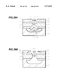
- FIGS. 53A and 53B illustrate conventional manufacture methods of a field emission element.
- a sacrificial film 103 is deposited by a deposition method having good step coverage.
- the sacrificial film 103 is deposited to have a cross section like a circle or ellipse so that a gentle slope is formed at this corner.
- the sacrificial film 103 deposited over the recess has an upward broadening taper shape.
- An emitter electrode (cathode) film 105 is deposited by using this sacrificial film 103 as a mold. After the substrate 101 under the emitter and the sacrificial film 103 are removed, the emitter electrode 105 having a sharp tip can be formed. If the radius of curvature of the tip A of the emitter electrode 105 becomes large depending upon the recess shape and the deposition conditions of the sacrificial film, an electric field is hard to concentrate and the electrical performance is not good.
- a sacrificial film 103 is deposited thick by a deposition method having poor step coverage, two side wall parts in cross section of the sacrificial film 103 swell and become partially in unison.
- an emitter electrode 105 having a relatively small apex angle of the emitter tip can be formed.
- the sacrificial film thick so that the tip of the emitter electrode is formed at an upper position above the substrate 101.
- a field emission element having a gate electrode in addition to an emitter electrode to be formed for example, a conductive film is formed on a substrate and a recess is formed in and through this conductive film. Therefore, this gate electrode is generally formed near at the boundary between the substrate 101 and the sacrificial film 103.
- the emitter electrode 105 is formed remotely from the gate electrode so that a high drive voltage of the field emission element is required and the electrical performance is lowered.
- a large radius of curvature of the emitter electrode tip makes an electric field hard to concentrate, lowering the performance of the field emission element.
- a relative position of the emitter and gate electrodes greatly influences the performance of the field emission element.
- a method of manufacturing a field emission element comprising: (a) forming an overhang portion on a substrate, the overhang portion having a cross section with confronting two parts; (b) depositing a first sacrificial film on the overhang portion with the two parts, the first sacrificial film being made of material capable of chemical reaction, having a cross section with two parts, and having a curved surface continuous from above the overhang portion to below the overhang portion; (c) depositing a reaction control film on the first sacrificial film thicker at an upper area of the first sacrificial film with the two parts than at a lower area of the first sacrificial film, the reaction control film having a cross section with two parts and controlling to decelerate chemical reaction of the first sacrificial film; (d) chemically reacting the first sacrificial film having the reaction control film to expand the volume of a lower region of the first sacrificial film more than an upper region thereof
- the first sacrificial film and the reaction control film having a thickness distribution are deposited on the overhang portion having the two parts in cross section, and thereafter chemical reaction is executed to expand the volume of the first sacrificial film locally and in a limited region.
- the two parts of the overhang portion become in contact with each other by the volume expansion in the limited region.
- a sharp valley or cusp portion is formed at this contact area, the cusp portion having a cross section like two contacted circles or ellipses.
- a method of manufacturing a field emission element comprising: (a) forming an overhang portion on a substrate, the overhang portion having a cross section with confronting two parts; (b) depositing a first sacrificial film on the overhang portion with the two parts, the first sacrificial film being made of material capable of chemical reaction, having a cross section with two parts, and having a curved surface continuous from above the overhang portion to below the overhang portion; (c) depositing a reaction control film on the first sacrificial film thicker at an upper area of the first sacrificial film with the two parts than at a lower area of the first sacrificial film, the reaction control film having a cross section with two parts and controlling to decelerate chemical reaction of the first sacrificial film; (d) reacting the first sacrificial film having the reaction control film to expand the volume of a lower region of the first sacrificial film more than an upper region thereof; (
- the first sacrificial film and the reaction control film having a thickness distribution are deposited on the overhang portion having the two parts in cross section, and thereafter chemical reaction is executed to expand the volume of the first sacrificial film locally and in a limited region. Thereafter, the insulating film is deposited to fill the gap between the two parts of the overhang portion. A sharp valley or cusp portion is formed at this contact area, the cusp portion having a cross section like two contacted circles or ellipses. Since the insulating film is thin, the film can be formed at high precision. By using this cusp portion as a mold, a field emission emitter having a small apex angle and radius of curvature of the emitter tip can be manufactured.
- a two-electrode structure may be incorporated in the field emission element, wherein: the first sacrificial film is made of semiconductor or conductive material; the step (d) performs chemically reacting only part of the first sacrificial film; the field emission cathode film is a field emission cathode made of conductive material; and the step (f) performs exposing a tip of the field emission cathode and an edge of an unreacted region of the first sacrificial film.
- the relative position of the emitter electrode and gate electrode can be set precisely by a proper combination of process conditions of the step of depositing a first sacrificial film on the overhang portion with the two parts, the step of depositing a reaction control film having a thickness distribution, and the step of chemically reacting the first sacrificial film.
- FIGS. 1A to 1H are diagrams illustrating the manufacture steps of a field emission element according to a first embodiment of the invention.
- FIGS. 2A to 2C are diagrams illustrating three methods of reinforcing an emitter electrode with a support substrate.
- FIGS. 3A and 3B are diagrams illustrating another method of forming a second sacrificial film.
- FIG. 4 is a diagram illustrating the manufacture steps of a two-electrode field emission element.
- FIG. 5A is a schematic diagram showing a relative position of emitter and gate electrodes
- FIG. 5B is a graph showing a relationship between a distance between emitter and gate electrodes and a maximum field intensity.
- FIGS. 6A to 6C are diagrams illustrating three methods of reinforcing a two-electrode field emission element with a support substrate.
- FIG. 7 is a diagram showing another example of a field emission element.
- FIGS. 8A and 8B are diagrams illustrating the manufacture steps of a three-electrode field emission element.
- FIG. 9 is a perspective view of a three-electrode field emission element.
- FIGS. 10A and 10B are diagrams showing the three-electrode field emission element shown in FIG. 9 turned upside down.
- FIG. 10A shows an emitter electrode having a needle-like tip
- FIG. 10B is a perspective view of an emitter electrode having a wedge-like tip extending in one direction.
- FIG. 11 is a diagram showing another three-electrode field emission element.
- FIGS. 12A to 12E are diagrams illustrating the manufacture steps of a field emission element according to a second embodiment of the invention.
- FIG. 13 is a diagram showing a two-electrode field emission element.
- FIGS. 14A and 14B are diagrams illustrating the manufacture steps of a three-electrode field emission element.
- FIG. 15 is a perspective view of a three-electrode field emission element.
- FIG. 16 is a diagram showing another three-electrode field emission element.
- FIGS. 17A to 17F are diagrams illustrating the manufacture steps of a field emission element according to a third embodiment of the invention.
- FIG. 18 is a diagram showing a two-electrode field emission element.
- FIGS. 19A and 19B are diagrams illustrating the manufacture steps of a three-electrode field emission element.
- FIGS. 20A to 20F are diagrams illustrating the manufacture steps of a field emission element according to a fourth embodiment of the invention.
- FIG. 21 is a diagram showing a two-electrode field emission element.
- FIGS. 22A and 22B are diagrams illustrating the manufacture steps of a three-electrode field emission element.
- FIGS. 23A to 23F are diagrams illustrating the manufacture steps of a field emission element according to a fifth embodiment of the invention.
- FIG. 24 is a diagram showing a two-electrode field emission element.
- FIGS. 25A and 25B are diagrams illustrating the manufacture steps of a three-electrode field emission element.
- FIGS. 26A to 26F are diagrams illustrating the manufacture steps of a field emission element according to a sixth embodiment of the invention.
- FIG. 27 is a diagram showing a two-electrode field emission element.
- FIG. 28 is a diagram showing another two-electrode field emission element.
- FIGS. 29A and 29B are diagrams illustrating the manufacture steps of a three-electrode field emission element.
- FIGS. 30A to 30I are diagrams illustrating the manufacture steps of a field emission element according to a seventh embodiment of the invention.
- FIGS. 31A and 31B are diagrams illustrating another method of forming a second sacrificial film.
- FIGS. 32A to 32C are diagrams illustrating another method of forming a second sacrificial film.
- FIG. 33 is a diagram illustrating the manufacture steps of a two-electrode field emission element.
- FIGS. 34A and 34B are diagrams illustrating the manufacture steps of a three-electrode field emission element.
- FIGS. 35A to 35C are diagrams illustrating the other manufacture steps of a three-electrode field emission element.
- FIGS. 36A to 36H are diagrams illustrating the manufacture steps of a field emission element according to an eighth embodiment of the invention.
- FIGS. 37A and 37B are diagrams illustrating another method of forming a second sacrificial film.
- FIG. 38 is a diagram illustrating the manufacture steps of a two-electrode field emission element.
- FIGS. 39A and 39B are diagrams illustrating the manufacture steps of a three-electrode field emission element.
- FIGS. 40A to 40C are diagrams illustrating the other manufacture steps of a three-electrode field emission element.
- FIGS. 41A and 41B illustrate a first definition of an emitter, using height as a parameter.
- FIG. 41A shows the shape of an one-stage type emitter
- FIG. 41B shows the shape of a multi-stage (two-stage) type emitter.
- FIGS. 42A and 42B illustrate a second definition of an emitter, using height as a parameter.
- FIG. 42A shows the shape of an one-stage type emitter
- FIG. 42B shows the shape of a multi-stage (two-stage) type emitter.
- FIGS. 43A and 43B illustrate a third definition of an emitter, using height as a parameter.
- FIG. 43A shows the shape of an one-stage type emitter
- FIG. 43B shows the shape of a multi-stage (two-stage) type emitter.
- FIGS. 44A and 44B illustrate a first definition of an emitter, using apex angle as a parameter.
- FIG. 44A shows the shape of an one-stage type emitter
- FIG. 44B shows the shape of a multi-stage (two-stage) type emitter.
- FIGS. 45A and 45B illustrate a second definition of an emitter, using apex angle as a parameter.
- FIG. 45A shows the shape of an one-stage type emitter
- FIG. 45B shows the shape of a multi-stage (two-stage) type emitter.
- FIGS. 46A and 46B illustrate a third definition of an emitter, using apex angle as a parameter.
- FIG. 46A shows the shape of an one-stage type emitter
- FIG. 46B shows the shape of a multi-stage (two-stage) type emitter.
- FIGS. 47A and 47B illustrate a first definition of an emitter, using cross sectional area as a parameter.
- FIG. 47A shows the shape of an one-stage type emitter
- FIG. 47B shows the shape of a multi-stage (two-stage) type emitter.
- FIGS. 48A and 48B illustrate a second definition of an emitter, using cross sectional area as a parameter.
- FIG. 48A shows the shape of an one-stage type emitter
- FIG. 48B shows the shape of a multi-stage (two-stage) type emitter.
- FIGS. 49A and 49B illustrate a third definition of an emitter, using cross sectional area as a parameter.
- FIG. 49A shows the shape of an one-stage type emitter
- FIG. 49B shows the shape of a multi-stage (two-stage) type emitter.
- FIG. 50 is a cross sectional view of a flat panel display using field emission elements.
- FIG. 51 is a perspective view partially in cross section of a flat panel display.
- FIG. 52 is a circuit diagram of a flat panel display.
- FIGS. 53A and 53B are cross sectional views of conventional field emission elements.
- FIGS. 1A to 1H are diagrams illustrating the manufacture steps of a field emission element according to the first embodiment of the invention. In the following, the manufacture steps of an emitter (cathode) constituting a field emission element will be described.
- a substrate 10 is structured by a starting substrate 10a and a lamination film 10b of about 140 nm thick stacked upon the starting substrate 10a.
- the starting substrate 10a is made of an Si substrate having a thickness of several tens to several hundreds ⁇ m
- the lamination film 10b is made of SiN x .
- silicon nitride has stoichiometry of Si 3 N 4
- a silicon nitride film deposited by CVD or the like has different stoichiometry shifted from Si 3 N 4 . This shift amount may be changed and such silicon nitride is expressed by SiN x . This is also applied to aluminum nitride.
- the lamination film 10b may be made of SiO 2 instead of SiN x .
- the starting substrate 10a may be made of Al. If Al is used, the lamination film 10b is made of AlN x , Al 2 O 3 , or the like. In the following, it is assumed that the starting substrate 10a is made of Si and the lamination film 10b is made of SiN x .
- a resist film having a predetermined pattern is formed on the lamination film 10b.
- the lamination film 10b is selectively etched to form a hole 12 shown in FIG. 1B in the lamination film 10b so that a surface of the starting substrate 10a is exposed from an aperture of the hole 12.
- a lamination film 10c having two opposing parts in cross section is therefore formed.
- the two parts in cross section are the right side lamination film 10c and the left side lamination film 10c as viewed in the cross section of FIG. 1B. These two parts are continuous in plan view.
- the above selective etching is performed by reactive ion etching (RIE) using SF 6 containing etching gas.
- the hole 12 has a diameter of about 0.5 ⁇ m and a depth of about 140 nm.
- the starting substrate 10a is wet etched to form a hole 12a in the starting substrate.
- a substrate 10d is therefore formed.
- the hole 12a forms a hollow space and has a diameter of about 1.5 ⁇ m and a depth of about 0.5 ⁇ m. Isotropical wet etching is performed through the hole 12 to etch the starting substrate 10a not only along the vertical direction of the substrate 10a but also along the horizontal direction in the cross-section of the starting substrate 10a. Therefore, the starting substrate 10a is etched partially at the underneath of the lamination film 10c.
- the lamination film 10c extends like a hood near at the hole 12a.
- an overhang portion 13 is therefore formed having two opposing parts in cross section separated along the horizontal direction of the substrate. The two opposing parts in section are called hereinafter simply "two parts".
- a first sacrificial film 15a made of, for example, polysilicon is deposited by CVD on the lamination film 10c with two parts. Conformability and the like of a polysilicon film formed by CVD can be controlled by a pressure, a substrate temperature, and the like during deposition. Either atmospheric pressure CVD or low pressure CVD may be used. At the same time, a first sacrificial film 15b is also deposited through an opening on the substrate 10d at the bottom of the hole 12a.
- the first sacrificial films 15a and 15b may be made of amorphous silicon, WSi x , MoSi x , TaSi x , Al, Ta, Mo, or Ti, instead of polysilicon. Sputtering may be used instead of CVD.
- the first sacrificial films 15a and 15b of amorphous silicon may be formed by a DC sputtering system using, as a target, polysilicon which contains P or B. For example, sputtering is performed under the conditions of a power of 1 kW and an Ar gas pressure of 8 mTorr.
- the two parts contact to be unison at the opening and above the lamination film 10c.
- deposition of the first sacrificial film 15 is stopped while the two parts still have a sufficient gap therebetween.
- second sacrificial films 16a and 16b made of, for example, SiO 2 , are anisotropically deposited on the first sacrificial films 15a and 15b by CVD or sputtering.
- Sputtering is a deposition method having anisotropy.
- Directivity may be controlled.
- CVD with chemical reaction of two or more gases has the characteristics that material is difficult to be deposited on the bottom of a deep recess.
- Directivity may be controlled by a pressure, a temperature or the like.
- the second sacrificial film 16a is deposited generally uniformly in thickness on the first sacrificial film 15a constituted of the two parts.
- the side wall of the two parts is thick at the upper area, and gradually reduces its thickness at the lower area.
- the bottom area of the overhang portion of the two parts is not deposited or very thinly deposited with the second sacrificial film 16a.
- the second sacrificial film 16b is deposited on the first sacrificial film 15b.
- SiO 2 is deposited by plasma CVD, for example, under the conditions of a temperature of 415° C., a power of 290 W, a pressure of 1.5 Torr, and flow rates of 100 sccm of SiH 4 , 500 sccm of N 2 O, and 500 sccm of N 2 .
- the second sacrificial films 16a and 16b may be made of Al 2 O 3 , Ta 2 O 5 , MoO x , or TiO 2 , in addition to SiO 2 .
- the second sacrificial film 16a made of SiO 2 functions to limit the amount of oxidant (oxygen or the like) supplied from the surface of the second sacrificial film 16a to the surface of the first sacrificial film 15a made of Si.
- the amount of oxidant supplied to the overhang portion of the first sacrificial film 15a is small at the area where the second sacrificial film is thick, and large at the area where the second sacrificial film is thin.
- oxidation reaction progresses more at the lower area than at the upper area.
- the reacted first sacrificial film 15a is silicon oxide.
- the deposited second sacrificial film 16a and reacted first sacrificial film 15a are collectively called a reacted film 16c.
- a reacted film 16d is formed on the substrate 10d.
- a first sacrificial film 15c is a left portion of the first sacrificial film 15a not oxidized, and is made of, for example, polysilicon.
- a cusp portion having an acute angle can be formed at the contact area as shown in FIG. 1F.
- This cusp portion has an acute angle area having a cross section like two contacted circles or ellipses. If oxidation continues after the opening is closed, the contact point of the two parts of the sacrificial film gradually moves up. However, since the upper side is formed with the thick second sacrificial film, the range of the contact point moving upward is limited. Even with this change of the contact point position, the apex angle at the contact area maintains an acute angle.
- an emitter electrode is formed.
- wet oxidation is performed by using a vertical furnace under the conditions of a furnace temperature of 850° C., a supply of H 2 gas at 30000 cc/min, and a supply of O 2 gas at 20000 cc/min.
- an emitter electrode 17 made of, for example, TiN is deposited on the reacted film 16c about 0.2 ⁇ m by reactive sputtering.
- the reactive sputtering is performed by using a DC sputtering system under the conditions of a power of 5 kW, a pressure of 4 mTorr, a target of Ti, a supply of N 2 gas at 84 sccm, and a supply of Ar gas at 56 sccm.
- the emitter electrode 17 may be made of Mo, Cr, Ti, or W, instead of TiN. CVD instead of sputtering may be used.
- the tip of the emitter electrode 17 is formed at the surface level of the lamination film 10c.
- the substrate 10d is wet etched by HF+HNO 3 +H 2 O, and thereafter the reacted film 16c is wet etched by HF+NH 4 F to expose the tip of the emitter electrode as shown in FIG. 1H.
- the tip of the emitter electrode 17 has a projection of 0.3 to 0.8 ⁇ m high, an apex angle of about 20° and a radius of curvature of about 10 nm.
- the radius of curvature and apex angle of the tip of the emitter electrode 17 can be made small so that an electric field concentrates easily at the tip of the emitter electrode.
- FIGS. 2A to 2C are diagrams illustrating three methods of reinforcing an emitter electrode 17 with a support substrate 18. Since the emitter electrode 17 is as thin as about 0.2 ⁇ m, it is desired to reinforce the emitter electrode 17 with the support substrate 18.
- FIG. 2A illustrates the first method.
- the bottom recess of the emitter electrode 17 is filled with a planarizing film 19a of, for example, an SOG film.
- the planarizing film 19a is abraded by chemical mechanical polishing (CMP) or by etch-back to planarize the bottom surface of the emitter electrode 17.
- CMP chemical mechanical polishing
- the planarizing film 19a may be formed by reflowing PSG or BPSG instead of using the SOG film.
- the support substrate 18 is made of, for example, glass, quartz, or Al 2 O 3 . Thereafter, the wet etching process illustrated in FIG. 1H is performed to expose the tip of the emitter electrode 17.
- FIG. 2B illustrates the second method.
- Adhesive 19b such as low melting point glass is reflowed on the emitter electrode in the state shown in FIG. 1G to adhere the emitter electrode 17 and a support substrate 18 together.
- the adhesive 19b also serves to planarize the bottom surface of the emitter electrode 17.
- Al may be used as the adhesive 19b.
- the emitter electrode 17 and support substrate 18 may be adhered by anodic bonding using electrostatic forces generated upon application of a high voltage of 1 kV and maintaining the temperature at 400 to 500° C.
- the adhesive 19b may be used as an emitter wiring. Thereafter, similar to the process shown in FIG. 1H, the tip of the emitter electrode is exposed by wet etching.
- FIG. 2C illustrates the third method.
- the bottom recess of the emitter electrode 17 is filled with a planarizing film 19a made of, for example, W.
- a planarizing film 19a made of, for example, W.
- TiN serves as an adhesive layer when W is-deposited by CVD. Since the strength of the emitter electrode is reinforced by W, the emitter electrode can be made thin.
- the planarizing film 19a is etched back to planarize the bottom surface of the emitter electrode 17.
- a support substrate 18 is adhered to the emitter electrode 17 by using adhesive 19b such as Al.
- adhesive 19b such as Al.
- the process of forming the second sacrificial film 16a shown in FIG. 1E is important for determining the shape of the emitter electrode.
- the second sacrificial film 16a has a function of a reaction control film.
- the second sacrificial film 16a may be formed by the following method.
- FIGS. 3A and 3B are diagrams illustrating another method of forming the second sacrificial film.
- second sacrificial films 16d and 16e are deposited thick by CVD or the like, as shown in FIG. 3A.
- the second sacrificial film 16d is controlled to have two parts.
- the side wall of the two parts of the second sacrificial film 16d is made thick at the upper area near the opening, and gradually reduces its thickness at the lower area.
- the surface of the second sacrificial film 16d is etched by a uniform amount by isotropic wet etching. Therefore, as shown in FIG. 3B, a desired thickness distribution of the second sacrificial film 16a can be obtained.
- the bottom area of the overhang portion of the second sacrificial film 16a can be made thin.
- the reacted films 16c and 16d are formed by wet oxidation. Instead of wet oxidation, these reacted films may be formed by nitridation.
- nitridation is performed under the conditions of a temperature of 1050° C., an RF power of 10 kW, a pressure of 130 Pa, and a supply of NH 3 at 1 slm.
- Other reactions capable of increasing the volume may also be used.
- the emitter electrode manufacture methods have been described so far.
- a method of manufacturing another type of a field emission element of a two-electrode element (so-called diode) will be described.
- the two-electrode element has a structure of two electrodes, emitter and gate.
- FIG. 4 is a diagram illustrate the method of manufacturing a two-electrode element.
- an element shown in FIG. 1G is formed by the above described processes.
- the substrate 10d, reacted film 16d, and part of the reacted film 16c are etched.
- the tip of the emitter electrode 17 is exposed.
- the first sacrificial film 15c is made of conductive polysilicon or amorphous silicon
- the first sacrificial film 15c which is unreacted, can be used as a gate electrode.
- the two-electrode element has two electrodes--the emitter electrode (field emission cathode) 17 and gate electrode (control electrode) 15c.
- the reacted film 16f electrically isolates the emitter electrode 17 and gate electrode 15c.
- the lamination film 10c may be removed by etching.
- a relative position of the emitter electrode 17 and gate electrode 15c plays an important role of a two-electrode element.
- a shorter distance between the emitter electrode 17 and gate electrode 15c is principally better. It is therefore desired to position the tip of the emitter electrode 17 near at a straight line interconnecting the two parts of the gate electrodes 15c.
- FIG. 5A is a schematic diagram showing the relative position of the gate electrode 15c and emitter electrode 17. The relative position is turned upside down from that shown in FIG. 4.
- a distance Zge is a distance from the tip of the emitter electrode 17 to the center of a thickness td of the gate electrode 15c, along an electron emission direction.
- FIG. 5B is a graph showing a relationship between the distance Zge and a maximum field intensity Emax at the tip of the emitter electrode, with the thickness td of the gate electrode 15c being fixed to 0.4 ⁇ m.
- the abscissa represents the distance Zge, and the ordinate represents the maximum field intensity Emax of the tip of the emitter electrode 17.
- This graph shows a change in the maximum field intensity Emax of the emitter electrode as the distance Zge between the emitter and gate electrodes is changed from--0.35 ⁇ m to 0.25 ⁇ m.
- the larger the maximum field intensity Emax the more the electric field concentrates on the tip of the emitter electrode and the more the performance of the field emission element is improved.
- the maximum field intensity Emax takes an extreme value of 1.16 ⁇ 10 7 V/cm. Namely, the optimum position of the tip of the emitter electrode 17 is slightly higher in FIG. 5A (slightly lower in FIG. 4) than the center of the thickness of the gate electrode.
- oxidation or nitridation is performed to expand the volume.
- the position of the tip of the emitter electrode 17 can be controlled precisely from the following reasons.
- a film formed by CVD becomes thick approximately proportional to time.
- a film formed by chemical reaction such as oxidation becomes thick approximately proportional to a square root of time.
- the film thickness tends to saturate as the time lapses.
- the film thickness can be controlled more finely and the tip position of the emitter electrode can be controlled more precisely, the more the time lapses.
- a film having a better uniform quality can be formed by oxidation than CVD.
- a reaction speed can be regulated by adjusting the thickness of the second sacrificial film 16a deposited on the first sacrificial film 15a. The thicker the second sacrificial film 16a, the slower the reaction speed of the first sacrificial film 15a. If the second sacrificial film 16a is made thin at the lower side of the overhang portion constituted of the two parts, the reaction at this area can be enhanced.
- the two-electrode element uses the emitter electrode 17 as a cathode and the gate electrode 15c as a control electrode. If the tip of the emitter electrode 17 is set to a proper position by controlling the reaction of the first sacrificial film 15a by the second sacrificial film 16a, electrons can be easily emitted from the tip of the emitter electrode 17 even at a low control voltage applied to the gate electrode.
- the two-electrode element has the emitter electrode 17 with a small apex angle and radius of curvature of the tip so that the performance of the field emission element can be improved.
- FIGS. 6A to 6C are diagrams illustrating three methods of reinforcing a two-electrode element with a support substrate 18.
- FIG. 6A illustrates the first method.
- a bottom recess of the emitter electrode 17 is filled with a planarizing film 19a of, for example, an SOG film, a PSG film, or a BPSG film.
- the planarizing film 19a is etched back by CMP to planarize the bottom surface of the emitter electrode 17.
- a support substrate 18 is adhered to the emitter electrode 17.
- the support substrate 18 is made of, for example, glass, quartz, or Al 2 O 3 .
- FIG. 6B illustrates the second method.
- Adhesive 19b such as low melting point glass is reflowed on the emitter electrode 17 to planarize the bottom surface of the emitter and adhere the emitter electrode 17 and a support substrate 18 together.
- Al may be used as the adhesive 19b to anodically bond the emitter electrode 17 and support substrate 18.
- FIG. 6C illustrates the third method.
- the bottom recess of the emitter electrode is filled with a planarizing film 19a made of, for example, W. Thereafter, the planarizing film 19a is etched back to planarize the bottom surface of the emitter electrode 17.
- a support substrate 18 is adhered to the emitter electrode 17 by using adhesive 19b such as Al.
- FIG. 7 is a diagram illustrating another method of manufacturing a two-electrode element.
- This two-electrode element has a gate electrode (first sacrificial film) 15c thicker than that of the two-electrode element shown in FIG. 4.
- the first sacrificial film is deposited thick and the second sacrificial film is deposited thin, by CVD or the like. Thereafter, oxidation is performed.
- the gap between the two parts constituting the overhang portion becomes considerably small. Therefore, even slight oxidation can make the two parts of the overhang portion in contact with each other. Since the first sacrificial film is oxidized only a little, the first sacrificial film not oxidized, i.e., the gate electrode 15c, becomes thick and the side projection thereof becomes large. The distance (gate hole) between the two parts constituting the gate electrode becomes small. Accordingly, electrons can be easily emitted from the tip of the emitter electrode even at a low gate-emitter control voltage. Similar advantages are also obtained by a three-electrode element to be described later.
- the sacrificial film 15a shown in FIG. 1D is anisotropically deposited on the lamination film 10c.
- anisotropically depositing the first sacrificial film 15a it becomes possible to make the upper area of the overhang portion thick and the lower area relatively thin. If the first sacrificial film is isotropically deposited, the first sacrificial film 15a deposited at the overhang portion becomes likely to be made in contact with the first sacrificial film deposited on the substrate 10d. It is therefore difficult to form the first sacrificial film 15a constituted of the two parts.
- the tip of the emitter electrode can be positioned further to the center of the thickness of the gate electrode, or at the level lower than the center of the thickness.
- FIGS. 8A and 8B are diagrams illustrating a method of manufacturing a three-electrode element (so-called triode).
- the three-electrode element has three electrodes, an anode electrode, an emitter electrode, and a gate electrode.
- the element shown in FIG. 1G is manufactured by the previously described processes.
- a resist film having a predetermined pattern (not shown) is formed on the emitter electrode 17.
- a resist pattern as a mask, slit openings 20 are formed on both sides of an emitter electrode 17a by RIE (reactive ion etching) using Cl 2 containing etchant.
- An emitter electrode 17b is formed at the outer sides of the slit openings 20.
- the diameter of the emitter electrode 17a is about 0.3 ⁇ m, and the depth of the slit openings 20 is about 0.2 ⁇ m.
- part of the reacted film 16c and the whole of the reacted film 16d are wet etched.
- HF+NH 4 F is used for wet etching the reacted films 16c and 16d made of SiO 2 .
- the gate electrode 15c is made of, for example, polysilicon.
- FIG. 9 is a perspective view of a three-electrode element.
- the emitter electrode 17a is integrally formed with the emitter electrode 17b.
- the gate electrode 15c has a circular hole or gate hole near at the tip of the emitter electrode 17a.
- the tip of the emitter electrode 17a has a needle-like sharp edge near at the gate hole of the gate electrode 15c.
- FIG. 10A is a perspective view showing the three-electrode element shown in FIG. 9 turned upside down, the emitter electrode 17a being viewed through the substrate via the gate hole of the gate electrode.
- the tip of the emitter electrode 17a has a needle-like sharp edge.
- the tip of the emitter electrode 17a may have different shapes.
- FIG. 10B is a perspective view showing a three-electrode element having a slit gate hole of the gate electrode 15c.
- the emitter electrode 17a has a wedge-like tip extending along the longitudinal direction of the gate hole.
- the three-electrode element shown in FIG. 9 has the emitter electrode 17 as a cathode and an anode electrode 10d wherein a positive potential is applied to the gate electrode 15c to emit electrons from the emitter electrode 17a toward the anode electrode 10d.
- the apex angle and radius of curvature of the tip of the emitter electrode 17a can be made small.
- the relative position of the emitter electrode 17a and gate electrode 15c can be controlled precisely.
- the lamination film 10c is made of insulating material such as SiN x . Next, forming the lamination film 10c by conductive material will be described.
- FIG. 11 is a cross sectional view showing another example of a three-electrode element.
- a lamination film (first gate electrode) 10g is made of conductive material such as WSi x , TaSi x , and MoSi x . Between the anode electrode 10e and lamination film 10g, an insulating film 10f made of SiO 2 , SiN x , or the like is formed. The manufacture method of this three-electrode element will be described next.
- the substrate 10 shown in FIG. 1A is constituted of the starting substrate 10a and the lamination film 10b made of insulating material and stacked on the starting substrate 10a.
- the three-electrode element shown in FIG. 11 on a substrate 10e made of, for example, Si, an insulating film 10f made of SiO 2 or the like and a lamination film 10g made of conductive material are sequentially laminated. Thereafter, the processes described previously are performed to manufacture the three-electrode element shown in FIG. 11.
- a lamination of the first gate electrode 10g and second gate electrode 15c forms a low resistance gate electrode.
- the gate electrodes 10g and 15c are electrically isolated from the anode electrode 10e by the insulating film 10f.
- the lamination film 10g is not necessarily made of conductive material, but it may be made of insulating material.
- the second sacrificial film as a reaction control film made of, for example, SiO 2 , is deposited.
- the second sacrificial film suppresses the supply amount of oxidant to the first sacrificial film and locally controls the reaction of the first sacrificial film.
- the second sacrificial film is made of SiO x N y instead of SiO 2 , the supply amount of oxidant can be reduced further.
- the second sacrificial film may be SiO 2 or SiO x N y .
- the x-y ratio of SiO x N y can be set as desired. If y is set to 0, SiO 2 is used, whereas if x is set to 0, SiN x is used.
- the second sacrificial film of SiO 2 or SiO x N y suppresses the supply amount of oxidant to the first sacrificial film and serves as a reaction control film. If the second sacrificial film is made of SiN x , oxidant hardly passes therethrough so that it serves as a reaction preventing film.
- the second sacrificial film made of SiO 2 has been described above. Next, the second sacrificial film made of SiN x will be described.
- FIGS. 12A to 12E are diagrams illustrating the manufacture steps of a field emission element according to the second embodiment of the invention. In the following, the manufacture steps of an emitter constituting a field emission element will be described.
- FIG. 12A illustrates the manufacture step after the steps of FIGS. 1A to 1C.
- a first sacrificial film 15a made of, for example, polysilicon is deposited by CVD on the lamination film 10c with two parts.
- a first sacrificial film 15b is also deposited through an opening on the substrate 10d at the bottom of the hole 12a.
- the first sacrificial film 15a is deposited uniformly thick on the upper surface of the lamination film 10c, and thin on the lower surface thereof. The two parts of the first sacrificial film 15a are maintained.
- the first sacrificial films 15a and 15b may be made of amorphous silicon, WSi x , MoSi x , TaSi x , Al, Ta, Mo, or Ti, instead of polysilicon.
- reaction preventing films 11a and 11b made of SiN x are deposited.
- the reaction preventing film 11a is anisotropically deposited on the first sacrificial film 15a with the two parts, covering the upper surface and the upper side surface of the overhang portion (first sacrificial film 15a). The lower surface and the lower side surface of the overhang portion are not deposited with the reaction preventing film 11a.
- the reaction preventing film 11b is deposited on the first sacrificial film 15b.
- the reaction preventing films 11a and 11b have a function of preventing oxidation reaction.
- a silicon nitride film functions to intercept most of oxygens and becomes a reaction preventing film of oxidation reaction.
- the reaction preventing films 11a and 11b of SiN x are deposited by plasma CVD, for example, under the conditions of a temperature of 415° C., a power of 300 W, a pressure of 1 Torr, and flow rates of 35 sccm of SiH 4 and 500 sccm of N 2 .
- the reaction preventing film 11a may be deposited thick.
- the reaction preventing film 11a is thereafter isotropically wet etched by a uniform amount from the surface thereof to obtain a desired thickness distribution.
- the reaction preventing film on the lower surface of the overhang portion, if any, can be reliably removed.
- the reaction preventing film 11a As a mask, the exposed portion of the first sacrificial film 5a is oxidized by wet oxidation.
- the upper surface and the upper side surface of the first sacrificial film 15a are covered with the reaction preventing film 11a, and the lower surface and the lower side surface thereof are not covered with the reaction preventing film 11a.
- Oxidation reaction is stopped at the area covered with the reaction preventing film 11a, and is enhanced at the area not covered with the reaction preventing film 11a. Namely, oxidation is enhanced at the lower surface and the lower side surface of the overhang portion and the volume of this area expands.
- a reacted film 16a of SiO 2 is formed as shown in FIG. 12C. The reacted film 16a contacts the two parts of the overhang portion.
- the first sacrificial film is not completely oxidized, but the first sacrificial film 15c sown in FIG. 12C is left.
- a reacted film 16b is formed on the substrate 10d.
- a cusp portion formed when the two parts contact each other has a shape of two-stage curves.
- the first stage curve is a curve formed by the mold of the reaction preventing film 11a at the upper area of the overhang portion.
- the second stage curve is a curve formed by the mold of the reaction preventing film 11a at the lower area of the overhang portion.
- the cusp portion formed when the two parts become in contact with each other has a sharp acute angle having a cross section like two contacted circles or ellipses. By using this cusp portion as a mold, a two-stage type emitter electrode is formed.
- an emitter electrode 17 made of, for example, TiN is deposited on the reacted film 16a and reaction preventing film 11a about 0.2 ⁇ m by reactive sputtering.
- the emitter electrode 17 may be made of Mo, Cr, Ti, or W, instead of TiN.
- CVD instead of sputtering may be used.
- the substrate 10d, reacted film 16a, and reaction preventing film 11a are wet etched to expose the emitter electrode.
- the reaction preventing film SiN x
- the reaction preventing film is formed on the first sacrificial film, and oxidation is executed by using the reaction preventing film as a mask.
- Use of the reaction preventing film can prevent reaction at the upper area of the overhang portion and allows only the lower area thereof to be reacted. As a result, the two-stage type emitter electrode 17 can be formed.
- the apex angle and radius of curvature of the tip of the two-stage type emitter electrode can be easily made smaller. Even if the mold having a small apex angle and radius of curvature is used, emitter material can be easily filled in the cusp portion of the mold so that the relative position between the emitter electrode and gate electrode can be determined precisely. If the apex angle and radius of curvature of the emitter electrode are made small, electric field can be easily concentrated on the emitter electrode so that the product uniformity, reproductivity, and performance of field emission elements can be improved.
- the mold for the one-stage type emitter electrode has an emitter area gradually narrowing from the base of the emitter electrode to the tip thereof. It is therefore difficult to film emitter material or form an emitter electrode film deep into the narrowed tip.
- the mold for the second-stage type emitter electrode has an emitter area defined by two-stage curves. Therefore, as compared to the one-stage type emitter electrode gradually narrowing toward the tip by using only the first stage curve only, a broad opening area can be provided at the boundary between the first and second-stage curves so that the emitter electrode can be easily formed deep into its tip. The tip of the second-stage emitter electrode is therefore difficult to be broken, and the shape of the mold can be formed with good reproductivity.
- the emitter electrode manufacture methods have been described so far. Next, a method of manufacturing another type of a field emission element of a two-electrode element will be described.
- FIG. 13 is a diagram illustrate the method of manufacturing a two-electrode element.
- an element shown in FIG. 12D is formed by the above described processes. Thereafter, the substrate 10d, reacted film 16a, and part of the reaction preventing film 11a are etched. By partially removing the reaction preventing film 11a and leaving the reaction preventing film 11e as shown in FIG. 13, the tip of the emitter electrode 17 is exposed.
- the first sacrificial film 15c is made of conductive polysilicon or amorphous silicon
- the first sacrificial film 15c which is unreacted, can be used as a gate electrode.
- the two-electrode element has two electrodes--the emitter electrode 17 and gate electrode 15c.
- the reaction preventing film 11e electrically isolates the emitter electrode 17 and gate electrode 15c.
- the lamination film 10c may be removed by etching.
- the position of the tip of the emitter electrode 17 can be controlled more precisely than volume expansion using CVD, from the reasons described above.
- the emitter electrode 17 of the two-stage type can be formed and the apex angle and radius of curvature of the tip can be easily made smaller. Even if the mold having a small apex angle and radius of curvature is used, emitter material can be easily filled in the cusp portion of the mold so that the relative position between the emitter electrode 17 and gate electrode 15c can be determined precisely. If the apex angle and radius of curvature of the emitter electrode are made small, electric field can be easily concentrated on the emitter electrode 17 so that the product uniformity, reproductivity, and performance of field emission elements can be improved.
- FIGS. 14A and 14B are diagrams illustrating a method of manufacturing a three-electrode element. First, the element shown in FIG. 14D is manufactured by the previously described processes.
- a resist film having a predetermined pattern (not shown) is formed on the emitter electrode 17.
- a resist pattern as a mask, slit openings 20 are formed on both sides of an emitter electrode 17a by RIE (reactive ion etching) using Cl 2 containing etchant.
- An emitter electrode 17b is formed at the outer sides of the slit openings 20.
- the diameter of the emitter electrode 17a is about 0.3 ⁇ m, and the depth of the slit openings 20 is about 0.2 ⁇ m.
- the reacted film 16a and part of the reaction preventing film 11a are wet etched to leave a reaction preventing film 11e, so that so that the emitter electrode 17a, gate electrode 15c, and anode electrode 10d are exposed.
- the gate electrode 15c is made of, for example, polysilicon.
- FIG. 15 is a perspective view of a three-electrode element.
- the emitter electrode 17a is integrally formed with the emitter electrode 17b.
- the gate electrode 15c has a circular hole or gate hole near at the tip of the emitter electrode 17a.
- the tip of the emitter electrode 17a has a needle-like sharp edge near at the gate hole of the gate electrode 15c.
- the three-electrode element has the emitter electrode 17 as a cathode and an anode electrode 10d wherein a positive potential is applied to the gate electrode 15c to emit electrons from the emitter electrode 17a toward the anode electrode 10d.
- the apex angle and radius of curvature of the tip of the emitter electrode 17a can be made small.
- the relative position of the emitter electrode 17a and gate electrode 15c can be controlled precisely.
- the lamination film 10c is made of insulating material such as SiN x .
- the lamination film 10c may be made of conductive material by using the structure shown in FIG. 11.
- an anode electrode 10e has an additional anode electrode 15d which was deposited on the anode electrode 10e when an gate electrode 15c was formed thick.
- the anode electrode 15d is made of, for example, polysilicon.
- reaction process such as oxidation is executed by masking the first sacrificial film with a reaction preventing film.
- reaction process is executed by forming another sacrificial film on the reaction preventing film and first sacrificial film, will be described.
- FIGS. 17A to 17F are diagrams illustrating the manufacture steps of a field emission element according to the third embodiment of the invention. In the following, the manufacture steps of an emitter constituting a field emission element will be described.
- FIG. 17A illustrates the manufacture step after the steps of FIGS. 1A to 1C.
- a first sacrificial film 15a made of, for example, polysilicon is deposited by CVD on the lamination film 10c with two parts.
- a first sacrificial film 15b is also deposited through an opening on the substrate 10d at the bottom of the hole 12a.
- the first sacrificial film 15a is deposited uniformly thick on the upper surface of the lamination film 10c, and thin on the lower surface thereof. The two parts of the first sacrificial film 15a are maintained.
- the first sacrificial films 15a and 15b may be made of amorphous silicon, WSi x , MoSi x , TaSi x , Al, Ta, Mo, or Ti, instead of polysilicon. Sputtering may be used in place of CVD.
- a reaction preventing film 11a made of, for example, SiN x is deposited on the first sacrificial film 15a.
- the reaction preventing film 11a is anisotropically deposited on the first sacrificial film 15a with the two parts, covering the upper surface and the upper side surface of the overhang portion (first sacrificial film 15a). The lower surface and the lower side surface of the overhang portion are not deposited with the reaction preventing film 11a.
- the reaction preventing film 11a has a function of preventing oxidation reaction.
- the reaction preventing film 11a may be deposited thick.
- the reaction preventing film 11a is thereafter isotropically wet etched by a uniform amount from the surface thereof to obtain a desired thickness distribution.
- the reaction preventing film on the lower surface of the overhang portion, if any, can be reliably removed.
- a second sacrificial film 16a made of, for example, SiO 2 is deposited by plasma CVD, covering the reaction preventing film 11a. As the second sacrificial film 16a is deposited, it reaches, via the gap between the two parts of the overhang portion, to the first sacrificial film 15b.
- the surface of the first sacrificial film 15a has three regions 61, 62, and 63.
- the region 61 is covered with the reaction preventing film 11a and second sacrificial film 16a, and positioned at the upper area of the overhang portion.
- the region 62 is covered with only the second sacrificial film 16a, and positioned at the slightly lower side area of the overhang portion.
- the region 63 is covered with no film and exposed, and positioned at the lower area of the overhang portion.
- the first sacrificial film 15a is oxidized by wet oxidation.
- the region 61 of the first sacrificial film 15a is covered with the reaction preventing film 11a so that oxygen is rarely supplied, whereas the exposed region 63 is supplied with a sufficient amount of oxygen.
- the region 62 is covered with the second sacrificial film 16a so that the supply amount of oxygen depends upon the thickness of the second sacrificial film 16a. The thicker the second sacrificial film 16a, the more the supply amount of oxygen.
- the oxidation reaction progress degrees in the three regions 61, 62, and 63 are different.
- the regions 63, 62, and 61 are oxidized more easily in this order.
- the region 63 with its surface being exposed is oxidized most.
- the region 61 covered with the reaction preventing film 11a is hardly oxidized.
- the volumes of the regions 63 and 62 of the first sacrificial film not covered with the reaction preventing film 11a expand.
- Oxidation reaction proceeds most at the lower side surface of the overhang portion at which the region 63 is positioned, and the two parts of the overhang portion at the lower side surface connect each other.
- a reacted film 16c with the connected two parts is shown in FIG. 17D.
- the oxidation reaction is stopped.
- the first sacrificial film 15a (FIG. 17C) is oxidized, it becomes SiO 2 and is integrated with the same material SiO 2 of the second sacrificial film 16a to thereby form the reacted film 16c (SiO 2 ) shown in FIG. 17D.
- the first sacrificial film is not completely oxidized, but the first sacrificial film 15c shown in FIG. 17D is left.
- the reacted film 16c is formed when the two parts of the overhang portion contact each other. A sharp cusp portion is formed at this contact area.
- the surface of the reacted film 16c has a shape of two-stage curves. The first curve is at the region where oxidation reaction is intercepted (at the upper area of the overhang portion), and the second curve is at the region where oxidation reaction is enhanced (at the lower area of the overhang).
- the cusp portion formed at the oxidation reaction enhanced region has a sharp acute angle having a cross section like two contacted circles or ellipses.
- an emitter electrode 17 made of, for example, TiN is deposited on the reacted film 16c about 0.2 ⁇ m by reactive sputtering.
- the emitter electrode 17 may be made of Mo, Cr, Ti, or W, instead of TiN.
- CVD instead of sputtering may be used.
- the substrate 10d and reacted film 16c are wet etched to expose the emitter electrode 17.
- the reaction preventing film (SiN x ) is formed on the first sacrificial film and then the second sacrificial film is formed. It is easy to make small the apex angle and radius of curvature of the tip of the two-stage type emitter electrode. Therefore, the performance of field emission elements can be improved.
- the emitter electrode manufacture methods have been described so far. Next, a method of manufacturing another type of a field emission element of a two-electrode element will be described.
- FIG. 18 is a diagram illustrate the method of manufacturing a two-electrode element.
- an element shown in FIG. 17E is formed by the above described processes. Thereafter, the substrate 10d and part of the reacted film 16c are etched. By partially removing the reacted film 16c and leaving the reacted film 16g as shown in FIG. 13, the tip of the emitter electrode 17 is exposed.
- the equipotential surface can be set to the proximity of the emitter electrode 17 so that the electric field at the emitter electrode tip becomes strong.
- the first sacrificial film 15c is made of conductive polysilicon or amorphous silicon
- the first sacrificial film 15c which is unreacted, can be used as a gate electrode.
- the two-electrode element has two electrodes--the emitter electrode 17 and gate electrode 15c.
- the reacted film 16g and reaction preventing film 11a electrically isolate the emitter electrode 17 and gate electrode 15c. Since the insulating film has a two-layer structure, the dielectric breakdown voltage can be improved, because a probability of a presence of pin hole or weak spot at the same area of the two layers is a product of two probabilities of the two layer.
- the reaction preventing film 11a may be made of conductive material.
- the lamination film 10c may be removed by etching.
- FIGS. 19A and 19B are diagrams illustrating a method of manufacturing a three-electrode element.
- the element shown in FIG. 17E is manufactured by the previously described processes. Thereafter, as shown in FIG. 19A, a resist film having a predetermined pattern (not shown) is formed on the emitter electrode 17.
- a resist film having a predetermined pattern (not shown) is formed on the emitter electrode 17.
- slit openings 20 are formed on both sides of an emitter electrode 17a by RIE using Cl 2 containing etchant.
- An emitter electrode 17b is formed at the outer sides of the slit openings 20.
- the diameter of the emitter electrode 17a is about 0.3 ⁇ m, and the depth of the slit openings 20 is about 0.2 ⁇ m.
- the reacted film 16d and part of the reacted film 16c are wet etched to leave a reacted film 16g, so that the emitter electrode 17a, gate electrode 15c, and anode electrode 10d are exposed.
- oxidation reaction is performed by forming the reaction preventing film on the first sacrificial film and further forming the second sacrificial film thereon.
- oxidation reaction is performed by forming the second sacrificial film on the first sacrificial film and then forming a reaction preventing film thereon.
- FIGS. 20A to 20F are diagrams illustrating the manufacture steps of a field emission element according to the fourth embodiment of the invention. In the following, the manufacture steps of an emitter constituting a field emission element will be described.
- FIG. 20A illustrates the manufacture step after the steps of FIGS. 1A to 1C.
- a first sacrificial film 15a made of, for example, polysilicon is deposited by CVD on the lamination film 10c with two parts.
- a first sacrificial film 15b is also deposited through an opening on the substrate 10d at the bottom of the hole 12a.
- the first sacrificial film 15a is deposited uniformly thick on the upper surface of the lamination film 10c, and thin on the lower surface thereof. The two parts of the first sacrificial film 15a are maintained.
- the first sacrificial films 15a and 15b may be made of amorphous silicon, WSi x , MoSi x , TaSi x , Al, Ta, Mo, or Ti, instead of polysilicon. Sputtering may be used in place of CVD.
- a second sacrificial film 16a made of, for example, SiO 2 is deposited on the surface of the first sacrificial film 15a by CVD.
- a second sacrificial film 16b is also deposited on the first sacrificial film 15b.
- the second sacrificial film 16a is deposited uniformly thick on the upper surface of the first sacrificial film 15a, and gradually reduces its thickness at the side surface of the overhang portion toward the lower side surface.
- the second sacrificial film is deposited by plasma CVD, for example, under the conditions of a temperature of 415° C., a power of 290 W, a pressure of 1.5 Torr, and flow rates of 100 sccm of SiH 4 , 500 sccm of N 2 O, and 500 sccm of N 2 .
- a reaction preventing film 11a made of, for example, SiN x , is deposited partially on the second sacrificial film 15a.
- the reaction preventing film 11a is deposited only on the upper surface and the upper side surface of the overhang portion with the two parts, and not deposited on the lower side surface thereof.
- the reaction preventing film 11a has a function of preventing oxidation reaction of the first sacrificial film 15a.
- a reaction preventing film 11b is deposited, via a gap between the two parts of the overhang portion, on the second sacrificial film 16b.
- the reaction preventing film 11a may be deposited thick.
- the reaction preventing film 11a is thereafter isotropically wet etched by a uniform amount from the surface thereof to obtain a desired thickness distribution.
- the reaction preventing film on the lower surface of the overhang portion, if any, can be reliably removed.
- the surface of the first sacrificial film 15a has three regions 61, 62, and 63.
- the region 61 is covered with the reaction preventing film 11a and second sacrificial film 16a, and positioned at the upper area of the overhang portion.
- the region 62 is covered with only the second sacrificial film 16a, and positioned at the lower side area of the overhang portion.
- the region 63 is covered with no film and exposed, and positioned at the lower area of the overhang portion.
- the first sacrificial film 15a is oxidized by wet oxidation.
- the region 61 of the first sacrificial film 15a is covered with the reaction preventing film 11a so that oxygen is rarely supplied, whereas the exposed region 63 is supplied with a sufficient amount of oxygen.
- the region 62 is covered with the second sacrificial film 16a so that the supply amount of oxygen depends upon the thickness of the second sacrificial film 16a. The thicker the second sacrificial film 16a, the more the supply amount of oxygen.
- the oxidation reaction progress degrees in the three regions 61, 62, and 63 are different.
- the regions 63, 62, and 62 are oxidized more easily in this order.
- the volumes of the regions 63 and 62 of the first sacrificial film not covered with the reaction preventing film 11a expand.
- Oxidation reaction proceeds most at the lower side surface of the overhang portion at which the region 63 is positioned, and the two parts of the overhang portion at the lower side surface connect each other.
- a reacted film 16c with the connected two parts is shown in FIG. 20D.
- the oxidation reaction is stopped.
- the reacted film 16c is formed when the two parts of the overhang portion contact each other.
- a sharp cusp portion is formed at this contact area.
- the first sacrificial film 15a As the first sacrificial film 15a (FIG. 20C) is oxidized, it becomes SiO 2 and is integrated with the same material SiO 2 of the second sacrificial film 16a to thereby form the reacted film 16c (SiO 2 ) shown in FIG. 20D.
- the first sacrificial film is not completely oxidized, but the first sacrificial film 15c shown in FIG. 20D is left.
- a reacted film 16d is also formed on the substrate 10d during the oxidation reaction.
- the cusp portion formed by the reacted film 16c and reaction preventing film 11a has a shape of two-stage curves.
- the first curve is formed by the mold of the reaction preventing film 11a
- the second curve is formed by the mold of the reacted film 16c.
- the cusp portion formed by the reacted film has a sharp acute angle having a cross section like two contacted circles or ellipses. By using this cusp portion as a mold, a two-stage type emitter electrode is formed.
- an emitter electrode 17 made of, for example, TiN is deposited on the reaction preventing film 11a and reacted film 16c about 0.2 ⁇ m by reactive sputtering.
- the emitter electrode 17 may be made of Mo, Cr, Ti, or W, instead of TiN.
- CVD instead of sputtering may be used.
- the substrate 10d, reacted film 16c, and reaction preventing film 11a are wet etched to expose the emitter electrode 17.
- the emitter electrode 17 is preferably reinforced by the methods illustrated in FIGS. 2A to 2C, because it is thin.
- oxidation reaction is performed by forming the second sacrificial film on the first sacrificial film and further forming the reaction preventing film thereon.
- the second sacrificial film or the reaction preventing film may be formed on the first sacrificial film.
- a buffer function can be given to the second sacrificial film.
- distortion is likely to be generated by deformation of the first sacrificial film and deformation of the reaction preventing film during the oxidation reaction or other processes because the substrate is once heated to a high temperature and thereafter cooled.
- This second sacrificial film functions as a buffer for absorbing such distortion.
- the emitter electrode manufacture methods have been described so far. Next, a method of manufacturing another type of a field emission element of a two-electrode element will be described.
- FIG. 21 is a diagram illustrate the method of manufacturing a two-electrode element.
- an element shown in FIG. 20E is formed by the above described processes.
- the substrate 10d, reacted film 16c, and reaction preventing film 11a are etched to leave a reaction preventing film lie and a reacted film 16e such as shown in FIG. 21 to thereby expose the tip of the emitter 17.
- the first sacrificial film 15c is made of conductive polysilicon or amorphous silicon
- the first sacrificial film 15c which is unreacted, can be used as a gate electrode.
- the two-electrode element has two electrodes--the emitter electrode 17 and gate electrode 15c.
- the reacted film 16e and reaction preventing film lie electrically isolate the emitter electrode 17 and gate electrode 15c. Since the insulating film has a two-layer structure, the dielectric breakdown voltage can be improved, because a probability of a presence of pin hole or weak spot at the same area of the two layers is a product of two probabilities of the two layer.
- the reaction preventing film lie may be made of conductive material.
- the lamination film 10c may be removed by etching.
- FIGS. 22A and 22B are diagrams illustrating a method of manufacturing a three-electrode element.
- the element shown in FIG. 20E is manufactured by the previously described processes. Thereafter, as shown in FIG. 22A, a resist film having a predetermined pattern (not shown) is formed on the emitter electrode 17. By using this resist pattern as a mask, slit openings 20 are formed on both sides of an emitter electrode 17a by RIE using Cl 2 containing etchant. An emitter electrode 17b is formed at the outer sides of the slit openings 20.
- the diameter of the emitter electrode 17a is about 0.3 ⁇ m, and the depth of the slit openings 20 is about 0.2 ⁇ m.
- reaction preventing film 11a and reacted film 16c are wet etched to leave a reaction preventing film 11e and a reacted film 16e, so that the emitter electrode 17a, gate electrode 15c, and anode electrode 10d are exposed.
- the second sacrificial film is formed on the surface of the first sacrificial film by CVD.
- CVD oxidation process is used for forming the second sacrificial film on the surface of the first sacrificial film.
- FIGS. 23A to 23F are diagrams illustrating the manufacture steps of a field emission element according to the fifth embodiment of the invention. In the following, the manufacture steps of an emitter constituting a field emission element will be described.
- FIG. 23A illustrates the manufacture step after the steps of FIGS. 1A to 1C.
- a first sacrificial film 15a made of, for example, polysilicon is anisotropically deposited by CVD on the lamination film 10c with two parts.
- a first sacrificial film 15b is also deposited through an opening on the substrate 10d at the bottom of the hole 12a.
- the first sacrificial film 15a is deposited uniformly thick on the upper surface of the lamination film 10c, and thin on the lower surface thereof. The two parts of the first sacrificial film 15a are maintained.
- the first sacrificial films 15a and 15b may be made of amorphous silicon, WSi x , MoSi x , TaSi x , Al, Ta, Mo, or Ti, instead of polysilicon. Sputtering may be used in place of CVD.
- the first sacrificial film 15c is oxidized by wet oxidation to uniformly form a second sacrificial film 16a made of, for example, SiO 2 on the surface of the first sacrificial film 15c.
- a second sacrificial film 16b is also formed on the surface of the substrate 10d.
- wet oxidation is performed by using a vertical furnace under the conditions of a furnace temperature of 850° C., a supply of H 2 gas at 30000 cc/min, and a supply of O 2 gas at 20000 cc/min.
- a reaction preventing film 11a made of, for example, SiN x , is anisotropically deposited on the second sacrificial film 16a.
- the reaction preventing film 11a is deposited on the upper surface and the upper side surface of the overhang portion with the two parts, and not deposited on the lower surface and the lower side surface thereof.
- a reaction preventing film 11b is also deposited on the second sacrificial film 16b.
- the reaction preventing films 11a and 11b have a function of preventing oxidation reaction.
- the reaction preventing film 11a may be deposited thick.
- the reaction preventing film 11a is thereafter isotropically wet etched by a uniform amount from the surface thereof to obtain a desired thickness distribution.
- the reaction preventing film on the lower surface of the overhang portion, if any, can be reliably removed.
- the surface of the first sacrificial film 15c has two regions 61 and 62.
- the region 61 is covered with the reaction preventing film 11a and second sacrificial film 16a, and positioned at the upper area of the overhang portion.
- the region 62 is covered with only the second sacrificial film 16a, and positioned at the lower area of the overhang portion.
- the first sacrificial film 15c is oxidized by wet oxidation.
- the region 61 of the first sacrificial film 15c is covered with the reaction preventing film 11a so that the oxidation reaction is prevented, whereas the region 62 is not covered with the reaction preventing film 11a 3 so that the oxidation reaction progresses.
- the oxidation speed is lowered depending upon the thickness of the second sacrificial film 16a.
- the second sacrificial film 16a controls not only the reaction of the first sacrificial film 15c, but also has a function of a buffer layer between the reaction preventing film 11a and first sacrificial film 15c similar to the fourth embodiment.
- the volume of the region 62 of the first sacrificial film not covered with the reaction preventing film 11a expand.
- the two parts of the overhang portion at the lower side surface connect each other.
- a reacted film 16c with the connected two parts is shown in FIG. 23D.
- the oxidation reaction is stopped.
- the reacted film 16c is formed when the two parts of the overhang portion contact each other.
- a sharp cusp portion is formed at this contact area.
- the first sacrificial film 15c As the first sacrificial film 15c (FIG. 23C) is oxidized, it becomes SiO 2 and is integrated with the same material SiO 2 of the second sacrificial film 16a to thereby form the reacted film 16c (SiO 2 ) shown in FIG. 23D.
- the first sacrificial film is not completely oxidized, but the first sacrificial film 15c shown in FIG. 23D is left.
- a reacted film 16d is also formed on the substrate 10d during the oxidation reaction.
- the cusp portion formed by the reacted film 16c and reaction preventing film 11a has a shape of two-stage curves.
- the first curve is formed by the mold of the reaction preventing film 11a
- the second curve is formed by the mold of the reacted film 16c.
- the cusp portion formed by the reacted film has a sharp acute angle having a cross section like two contacted circles or ellipses. By using this cusp portion as a mold, a two-stage type emitter electrode is formed.
- an emitter electrode 17 made of, for example, TiN is deposited on the reaction preventing film 11a and reacted film 16c about 0.2 ⁇ m by reactive sputtering.
- the emitter electrode 17 may be made of Mo, Cr, Ti, or W, instead of TiN.
- CVD instead of sputtering may be used.
- the substrate 10d, reacted film 16c, and reaction preventing film 11a are wet etched to expose the emitter electrode 17.
- the emitter electrode 17 is preferably reinforced by the methods illustrated in FIGS. 2A to 2C, because it is thin.
- the second sacrificial film is formed uniformly on the surface of the first sacrificial film by oxidation reaction, and thereafter the reaction preventing film is formed.
- the apex angle and radius of curvature of the tip of can be easily made smaller. Even if the mold having a small apex angle and radius of curvature is used, emitter material can be easily filled in the cusp portion of the mold so that the relative position between the emitter electrode 17 and gate electrode 15c can be determined precisely. If the apex angle and radius of curvature of the emitter electrode are made small, electric field can be easily concentrated on the emitter electrode 17 so that the product uniformity, reproductivity, and performance of field emission elements can be improved.
- the emitter electrode manufacture methods have been described so far. Next, a method of manufacturing another type of a field emission element of a two-electrode element will be described.
- FIG. 24 is a diagram illustrate the method of manufacturing a two-electrode element.
- an element shown in FIG. 23E is formed by the above described processes.
- the substrate 10d, reacted film 16c, and reaction preventing film 11a are etched to leave a reaction preventing film 11d and a reacted film 16e such as shown in FIG. 24 to thereby expose the tip of the emitter 17.
- the first sacrificial film 15e is made of conductive polysilicon or amorphous silicon
- the first sacrificial film 15e which is unreacted, can be used as a gate electrode.
- the two-electrode element has two electrodes--the emitter electrode 17 and gate electrode 15e.
- the reacted film 16e and reaction preventing film 11d electrically isolate the emitter electrode 17 and gate electrode 15e. Since the insulating film has a two-layer structure, the dielectric breakdown voltage can be improved, because a probability of a presence of pin hole or weak spot at the same area of the two layers is a product of two probabilities of the two layer.
- the reaction preventing film 11d may be made of conductive material.
- the lamination film 10c may be removed by etching.
- FIGS. 25A and 25B are diagrams illustrating a method of manufacturing a three-electrode element.
- the element shown in FIG. 23E is manufactured by the previously described processes. Thereafter, as shown in FIG. 25A, a resist film having a predetermined pattern (not shown) is formed on the emitter electrode 17. By using this resist pattern as a mask, slit openings 20 are formed on both sides of an emitter electrode 17a by RIE using Cl 2 containing etchant. An emitter electrode 17b is formed at the outer sides of the slit openings 20.
- the diameter of the emitter electrode 17a is about 0.3 ⁇ m, and the depth of the slit openings 20 is about 0.2 ⁇ m.
- reaction preventing film 11a and reacted film 16c are wet etched to leave a reaction preventing film 11d and a reacted film 16e, so that the emitter electrode 17a, gate electrode 15e, and anode electrode 10d are exposed.
- the second sacrificial film and reaction preventing film are formed on the surface of the first sacrificial film, and thereafter oxidation reaction is performed.
- the reaction preventing film is formed on the first sacrificial film, oxidation reaction is performed, and then an insulating film is formed on the surface of an emitter electrode forming mold.
- FIGS. 26A to 26F are diagrams illustrating the manufacture steps of a field emission element according to the sixth embodiment of the invention. In the following, the manufacture steps of an emitter constituting a field emission element will be described.
- FIG. 26A illustrates the manufacture step after the steps of FIGS. 1A to 1C.
- a first sacrificial film 15a made of, for example, polysilicon is anisotropically deposited by CVD on the lamination film 10c with two parts.
- a first sacrificial film 15b is also deposited through an opening on the substrate 10d at the bottom of the hole 12a.
- the first sacrificial film 15a is deposited uniformly thick on the upper surface of the lamination film 10c, and thin on the lower surface thereof. The two parts of the first sacrificial film 15a are maintained.
- the first sacrificial films 15a and 15b may be made of amorphous silicon, WSi x , MoSi x , TaSi x , Al, Ta, Mo, or Ti, instead of polysilicon. Sputtering may be used in place of CVD.
- a reaction preventing film 11a made of, for example, SiN x is anisotropically deposited on the first sacrificial film 15a.
- the reaction preventing film 11a is deposited on the upper surface and the upper side surface of the overhang portion (first sacrificial film 15a), and not deposited on the lower surface and the lower side surface thereof.
- a reaction preventing film 11b is also deposited on the first sacrificial film 15b.
- the reaction preventing films 11a and 11b have a function of preventing oxidation reaction.
- the reaction preventing film 11a may be deposited thick.
- the reaction preventing film 11a is thereafter isotropically wet etched by a uniform amount from the surface thereof to obtain a desired thickness distribution.
- the reaction preventing film on the lower surface of the overhang portion, if any, can be reliably removed.
- the reaction preventing film 11a As a mask, the exposed portion of the first sacrificial film 15a is oxidized by wet oxidation.
- the upper surface and the upper side surface of the first sacrificial film 15a are covered with the reaction preventing film 11a, and the lower surface and the lower side surface thereof are not covered with the first reaction preventing film 11a. Oxidation reaction at the region covered with the reaction preventing film 11a is stopped, whereas it is progressed at the lower surface and the lower side surface of the overhang portion to effect volume expansion.
- Oxidation process continues until the two parts of the overhang portion are connected each other by the volume expansion at the lower regions of the overhang portion.
- a reacted film 16a of SiO 2 such as shown in FIG. 26C is formed.
- the reacted film 16a connects the two parts of the overhang portion.
- the first sacrificial film is not completely oxidized, but the first sacrificial film 15c shown in FIG. 26C is left.
- a reacted film 16b is also formed on the substrate 10d during the oxidation reaction.
- the cusp portion formed by the reacted film 16a and reaction preventing film 11a has a shape of two-stage curves.
- the first curve is formed by the mold of the reaction preventing film 11a
- the second curve is formed by the mold of the reacted film 16a.
- the cusp portion formed by the reacted film 16a has a sharp acute angle having a cross section like two contacted circles or ellipses.
- an insulating film 16c made of, for example, SiO 2 is isotropically deposited on the surface of the cusp portion formed by the reaction preventing film 11a and reacted film 16a.
- the insulating film 16c has a shape conformal to the shape of the cusp portion formed by the two-stage curves.
- This insulating film 16c serves to adjust the shape of the cusp portion, i.e., the shape of an emitter electrode forming mold. For example, it can adjust the height and width of the emitter electrode.
- the reacted film 16a is not necessarily required to connect the two parts of the overhang. Even if the reacted film 16a is separated to have two parts, the insulating film 16c can fill the gap between the two parts of the reacted film 16a.
- the oxidation reaction may be stopped immediately before the two parts of the overhang connect each other. It is sufficient if the two parts of the overhang portion at the lower side surface are expanded in volume to form two projected portions. With these projected portions and the insulating film, the cusp portion of the two-stage type can be formed.
- an emitter electrode 17 made of, for example, TiN is deposited on the insulating film 16c about 0.2 ⁇ m by reactive sputtering.
- the emitter electrode 17 may be made of Mo, Cr, Ti, or W, instead of TiN.
- CVD or evaporation instead of sputtering may be used.
- the insulating film 16c is wet etched to expose the emitter electrode 17.
- the emitter electrode 17 is preferably reinforced by the methods illustrated in FIGS. 2A to 2C, because it is thin.
- the first sacrificial film is oxidized to form the emitter electrode forming mold by using the reaction preventing film as a mask, and thereafter the insulating film is deposited on the surface of this mold.
- the apex angle and radius of curvature of the tip of can be easily made smaller. Even if the mold having a small apex angle and radius of curvature is used, emitter material can be easily filled in the cusp portion of the mold so that the relative position between the emitter electrode 17 and gate electrode 15c can be determined precisely. If the apex angle and radius of curvature of the emitter electrode are made small, electric field can be easily concentrated on the emitter electrode 17 so that the product uniformity, reproductivity, and performance of field emission elements can be improved.
- the emitter electrode manufacture methods have been described so far. Next, a method of manufacturing another type of a field emission element of a two-electrode element will be described.
- FIG. 27 is a diagram illustrate the method of manufacturing a two-electrode element.
- an element shown in FIG. 26E is formed by the above described processes.
- the substrate 10d, reacted film 16a, reaction preventing film 11a, and insulating film 16c are etched to leave an insulating film 16e and a reaction preventing film 11e such as shown in FIG. 27 to thereby expose the tip of the emitter 17.
- the first sacrificial film 15c is made of conductive polysilicon or amorphous silicon
- the first sacrificial film 15c which is unreacted, can be used as a gate electrode.
- the two-electrode element has two electrodes--the emitter electrode 17 and gate electrode 15c.
- the insulating film 16e and reaction preventing film 11e electrically isolate the emitter electrode 17 and gate electrode 15c.
- the reaction preventing film 11e may be made of conductive material.
- the lamination film 10c may be removed by etching.
- FIG. 28 shows another example of the two-electrode element.
- the reaction preventing film 11a is left unetched, whereas in the two-electrode element shown in FIG. 27, part of the reaction preventing film 11e is left. Namely, only the insulation film (SiO 2 ) is etched and the reaction preventing film (SiN x ) is not etched. Therefore, part of the insulating film 16e and the whole of the reaction preventing film 11a are left.
- the reaction preventing film 11a is located between the emitter electrode 17 and the gate electrode 15c to prevent leak current from flowing between the emitter electrode 17 and the gate electrode 15c.
- the two-electrode element shown in FIG. 27 has a drawback that if foreign dielectric substance is captured between the emitter electrode 17 and gate electrode 15c, leak current is likely to flow between the emitter electrode 17 and the gate electrode 15c. Such a drawback is not associated with the two-electrode element shown in FIG. 28.
- the equipotential surface (line) can be set to the proximity of the emitter electrode 17 so that the electric field at the emitter electrode tip becomes strong.
- FIGS. 29A and 29B are diagrams illustrating a method of manufacturing a three-electrode element.
- the element shown in FIG. 26E is manufactured by the previously described processes. Thereafter, as shown in FIG. 29A, a resist film having a predetermined pattern (not shown) is formed on the emitter electrode 17. By using this resist pattern as a mask, slit openings 20 are formed on both sides of an emitter electrode 17a by RIE using Cl 2 containing etchant. An emitter electrode 17b is formed at the outer sides of the slit openings 20.
- the diameter of the emitter electrode 17a is about 0.3 ⁇ m, and the depth of the slit openings 20 is about 0.2 ⁇ m.
- the insulating film 16c and reaction preventing film 11a are wet etched to leave an insulating film 16e and a reaction preventing film 11e, so that the emitter electrode 17a, gate electrode 15c, and anode electrode 10d are exposed.
- FIGS. 30A to 30I are diagrams illustrating the manufacture steps of a field emission element according to the seventh embodiment of the invention. In the following, the manufacture steps of an emitter (cathode) constituting a field emission element will be described.
- a substrate 10 is structured by a starting substrate 10a and a lamination film 10b of about 140 nm thick stacked upon the starting substrate 10a.
- the starting substrate 10a is made of Si
- the lamination film 10b is made of SiN x .
- the lamination film 10b may be made of SiO 2 instead of SiN x .
- the starting substrate 10a may be made of Al. If Al is used, the lamination film 10b is made of AlN x , Al 2 O 3 , or the like. In the following, it is assumed that the starting substrate 10a is made of Si and the lamination film 10b is made of SiN x .
- a resist film having a predetermined pattern is formed on the lamination film 10b.
- the lamination film 10b is selectively etched to form a hole 12 shown in FIG. 30B in the lamination film 10b so that a surface of the starting substrate 10a is exposed from an aperture of the hole 12.
- a lamination film 10c having two opposing parts in cross section is therefore formed.
- the above selective etching is performed by RIE using SF 6 containing etching gas.
- the hole 12 has a diameter of about 0.5 ⁇ m and a depth of about 140 nm.
- the starting substrate 10a is wet etched to form a hole 12a in the starting substrate.
- a substrate 10d is therefore formed.
- the hole 12a forms a hollow space and has a diameter of about 1.5 ⁇ m and a depth of about 0.5 ⁇ m. Isotropical wet etching is performed through the hole 12 to etch the starting substrate 10a not only along the vertical direction of the substrate 10a but also along the horizontal direction in the cross-section of the starting substrate 10a. Therefore, the starting substrate 10a is etched partially at the underneath of the lamination film 10c.
- the lamination film 10c extends like a hood near at the hole 12a. As shown in FIG. 30C, an overhang portion 13 is therefore formed having two opposing parts in cross section separated along the horizontal direction of the substrate.
- a first sacrificial film 15a made of, for example, polysilicon is deposited by CVD on the lamination film 10c with two parts.
- a first sacrificial film 15b is also deposited through an opening on the substrate 10d at the bottom of the hole 12a.
- the first sacrificial films 15a and 15b may be made of amorphous silicon, WSi x , MoSi x , TaSi x , Al, Ta, Mo, or Ti, instead of polysilicon. Sputtering may be used instead of CVD.
- the first sacrificial films 15a and 15b of amorphous silicon may be formed by a DC sputtering system using, as a target, polysilicon which contains P or B. For example, sputtering is performed under the conditions of a power of 1 kW and an Ar gas pressure of 8 mTorr.
- second sacrificial films 16a and 16b made of, for example, SiO 2 , are deposited by plasma CVD.
- the second sacrificial film 16a is isotropically deposited on the first sacrificial film 15a with the two parts. The bottom area of the overhang portion of the two parts is rarely deposited with the second sacrificial film 16a.
- the second sacrificial film 16b is deposited on the first sacrificial film 15b.
- the second sacrificial films 16a and 16b may be made of Al 2 O 3 , Ta 2 O 5 , MoO x , or TiO 2 , in addition to SiO 2 .
- P ions are diffused partially into the first sacrificial films 15a and 15b by vapor phase thermal diffusion to form diffused regions 15c and 15d.
- the second sacrificial films serve as a mask for vapor phase thermal diffusion.
- P ions start diffusing from the regions not covered with the second sacrificial films 16a and 16b, while the second sacrificial films 16a and 16b function to stop impurity diffusion.
- the regions 15c and 15d are P-ion diffused regions.
- the diffused regions 15c is formed only on the bottom surface of the overhang, i.e., at the lower area thereof.
- Vapor phase thermal diffusion may be performed under the conditions of a temperature of 850° C. and flow rates of 20 slm of N 2 , 0.1 slm of O 2 , and 0.05 g/min of POCl 3 .
- Doped impurities may be B or As instead of P.
- a first sacrificial film 15e is the first sacrificial film 15a shown in FIG. 30F and not oxidized.
- wet oxidation is performed by using a vertical furnace under the conditions of a furnace temperature of 850° C., a supply of H 2 gas at 30000 cc/min, and a supply of O 2 gas at 20000 cc/min.
- the reacted films 16c and 16d are made of SiO 2 . If the first sacrificial films 15a and 15b are made of Al, the reacted films 16c and 16d are Al 2 O 3 .
- the surface of the overhang portion includes the second sacrificial film 16a and the diffused region 15c.
- the oxidation speed of the diffused region 15c of the first sacrificial film 15a is about two times faster than the other region of the first sacrificial film 15a.
- the volume of the overhang expands less at the upper area than at the lower area, and the two parts of the overhang become in contact with each other.
- the cusp portion formed at the contact area of the two parts has a shape of two-stage curves and can form an acute angle.
- This cusp portion has an acute angle area having a cross section like two contacted circles or ellipses.
- an emitter electrode 17 made of, for example, TiN is deposited on the reacted film 16c about 0.2 ⁇ m by reactive sputtering.
- the reactive sputtering is performed by using a DC sputtering system under the conditions of a power of 5 kW, a pressure of 4 mTorr, a target of Ti, a supply of N 2 gas at 84 sccm, and a supply of Ar gas at 56 sccm.
- the emitter electrode 17 may be made of Mo, Cr, Ti, or W, instead of TiN. CVD or evaporation instead of sputtering may be used.
- the substrate 10d is wet etched by HF+HNO 3 +H 2 O, and thereafter the reacted film 16c is wet etched by HF+NH 4 F to expose the tip of the emitter electrode as shown in FIG. 30I.
- the emitter electrode 17 of the two-stage type can be formed.
- This emitter electrode may be reinforced by the methods illustrated in FIGS. 2A to 2C, because it is thin.
- the process of forming the second sacrificial film 16a shown in FIG. 30E is important for determining the shape of the emitter electrode.
- the second sacrificial film 16a may be formed by the following method.
- FIGS. 31A and 31B are diagrams illustrating another method of forming the second sacrificial film.
- second sacrificial films 16g and 16h are deposited thick by plasma CVD or the like, as shown in FIG. 31A.
- the second sacrificial film 16g is controlled to have two parts.
- the surface of the second sacrificial film 16g is etched by a uniform amount by isotropic wet etching. Therefore, as shown in FIG. 31B, a desired thickness distribution of the second sacrificial film 16a can be obtained. The bottom area of the overhang portion of the second sacrificial film 16a can be made thin. Thereafter, the processes starting from FIG. 30F are executed.
- FIGS. 32A to 32C are diagrams illustrating a method of adjusting the thickness of the second sacrificial film after impurities are doped in the second sacrificial film.
- second sacrificial films 16g and 16h are deposited thick by plasma CVD or the like.
- the second sacrificial film 16g is controlled to have two parts.
- P ions are diffused partially into the first sacrificial films 15a and 15b by thermal diffusion to form a diffused region 15c.
- P ions start diffusing from the region of the first sacrificial films 15a and 15b not covered or thinly covered with the second sacrificial films 16g.
- the region 15c is P-ion diffused region.
- the diffused regions 15c is formed only on the bottom surface of the overhang, i.e., at the lower area thereof.
- the surface of the second sacrificial film 16a is etched by a uniform amount by isotropic wet etching. Therefore, as shown in FIG. 32C, the second sacrificial film 16g is made thin at the bottom surface of the overhang portion, and maintained unchanged at the upper surface thereof. Thereafter, the processes starting from FIG. 30G are executed.
- the reacted film 16c is formed by wet oxidation.
- a reacted film 16c of SiN x may be formed by nitridation.
- nitridation is performed under the conditions of a temperature of 1050° C., an RF power of 10 kW, a pressure of 130 Pa, and a supply of NH 3 at 1 slm.
- the emitter electrode manufacture methods have been described so far. Next, a method of manufacturing another type of a field emission element of a two-electrode element will be described.
- FIG. 33 is a diagram illustrate the method of manufacturing a two-electrode element.
- an element shown in FIG. 30H is formed by the above described processes.
- the substrate 10d, reacted film 16d, and part of the reacted film 16c are etched.
- the tip of the emitter electrode 17 is exposed.
- the first sacrificial film 15e is made of conductive polysilicon or amorphous silicon
- the first sacrificial film 15e which is unreacted, can be used as a gate electrode.
- the two-electrode element has the emitter electrode 17 and gate electrode 15c.
- the reacted film 16e electrically isolates the emitter electrode 17 and gate electrode 15e.
- the lamination film 10c may be removed by etching.
- the first sacrificial film 15a anisotropically deposited on the lamination film 10c as illustrated in FIG. 30D may be isotropically deposited.
- anisotropical deposition makes the diameter of a hole (gate hole) of the gate electrode small so that the electrical performance can be improved.
- the gate electrode (first sacrificial film) of the two-electrode element shown in FIG. 33 is made thick, the diameter of the gate hole becomes small.
- the first sacrificial film 15a is anisotropically deposited. Anisotropical deposition of the first sacrificial film 15a can make the gate hole diameter small. Therefore, electrons can be emitted from the emitter even at a low gate-emitter voltage. Similar advantages are also obtained by a three-electrode element.
- the first sacrificial film 15a on the overhang portion and the first sacrificial film 15b on the substrate 10d become likely to be integrated together and the first sacrificial film 15a with two parts is difficult to form.
- the seventh embodiment after the first sacrificial film is formed, impurities are diffused only into the lower region of the overhang portion, and oxidation or nitridation is performed to expand the volume of the overhang portion.
- the position of the tip of the emitter electrode can therefore be controlled more precisely than volume expansion using CVD, from the reasons already described above.
- the two-electrode element has the emitter electrode 17 as a cathode and the gate electrode 15c as a control electrode. If the tip of the emitter electrode 17 is positioned properly, electrons can be emitted easily from the tip of the emitter electrode even at a low control voltage applied to the gate electrode.
- emitter material can be easily filled in the cusp portion of the mold so that the relative position between the emitter electrode 17 of the two-stage type and gate electrode 15c can be determined precisely. Since the apex angle and radius of curvature of the emitter electrode can be made small, the product uniformity, reproductivity, and performance of field emission elements can be improved.
- the two-electrode element may be reinforced by a support plate 18 by the methods illustrated in FIGS. 6A to 6C.
- FIGS. 34A and 34B are diagrams illustrating a method of manufacturing a three-electrode element. First, the element shown in FIG. 30H is manufactured by the previously described processes.
- a resist film having a predetermined pattern (not shown) is formed on the emitter electrode 17.
- a resist pattern As a mask, slit openings 20 are formed on both sides of an emitter electrode 17a by RIE using Cl 2 containing etchant.
- An emitter electrode 17b is formed at the outer sides of the slit openings 20.
- the diameter of the emitter electrode 17a is about 0.3 ⁇ m, and the depth of the slit openings 20 is about 0.2 ⁇ m.
- part of the reacted film 16c and the whole of the reacted film 16d are wet etched.
- HF+NH 4 F is used for wet etching the reacted films 16c and 16d made of SiO 2 .
- Part of the reacted film 16c is etched and a reacted film 16f is left unetched as shown in FIG. 34B so that the emitter electrode 17a, gate electrode 15e, and anode electrode 10d are exposed.
- the three-electrode element shown in FIG. 34B has the emitter electrode 17 as a cathode and an anode electrode 10d as an anode wherein a positive potential is applied to the gate electrode 15e to emit electrons from the emitter electrode 17a toward the anode electrode 10e.
- the apex angle and radius of curvature of the tip of the emitter electrode 17a can be made small, because even if the mold having a small apex angle and radius of curvature is used, emitter material can be easily filled in the cusp portion.
- the relative position of the emitter electrode 17a and gate electrode 15e can be controlled precisely. The strength of the tip of the emitter electrode can be retained.
- the lamination film 10c is made of insulating material such as SiN x . Next, forming the lamination film 10c by conductive material will be described.
- FIG. 35A is a cross sectional view showing another example of a three-electrode element.
- a lamination film (first gate electrode) log is made of conductive material such as WSi x , TaSi x , and MoSi x .
- an insulating film 10f made of SiO 2 , SiN x , or the like is formed between the anode electrode 10e and lamination film 10g. The manufacture method of this three-electrode element will be described next.
- the substrate 10 shown in FIG. 30A is constituted of the starting substrate 10a and the lamination film 10b made of insulating material and stacked on the starting substrate 10a.
- the three-electrode element shown in FIG. 35A on a substrate 10e made of, for example, Si, an insulating film 10f made of SiO 2 or the like and a lamination film 10g made of conductive material are sequentially laminated. Thereafter, the processes described previously are performed to manufacture the three-electrode element shown in FIG. 35A.
- a lamination of the first gate electrode log and second gate electrode 15e forms a low resistance gate electrode.
- the gate electrodes 10g and 15e are electrically isolated from the anode electrode 10e by the insulating film 10f.
- a lamination film 10c made of insulating material is used instead of the lamination film 10g of the three-electrode element made of conductive material and shown in FIG. 35A.
- the lamination film 10c may be made of SiN x , SiO 2 , AlN x , Al 2 O 3 , or the like.
- the gate electrode 15e and the anode electrode 10e are electrically isolated by the insulating films 10c and 10f.
- an anode electrode 10h is added to the anode electrode 10d of the three-electrode element shown in FIG. 34B.
- the anode electrode 10h is left when the gate electrode 15e is deposited thick, and is made of, for example, polysilicon.
- the anode electrode is therefore constituted of the electrode 10h stacked upon the electrode 10d.
- FIGS. 36A to 36H are diagrams illustrating the manufacture steps of a field emission element according to the eighth embodiment of the invention. In the following, the manufacture steps of an emitter (cathode) constituting a field emission element will be described.
- a substrate 10 is structured by a starting substrate 10a and a lamination film 10b of about 140 nm thick stacked upon the starting substrate 10a.
- the starting substrate 10a is made of Si
- the lamination film 10b is made of SiN x .
- the lamination film 10b may be made of SiO 2 instead of SiN x .
- the starting substrate 10a may be made of Al. If Al is used, the lamination film 10b is made of AlN x , Al 2 O 3 , or the like. In the following, it is assumed that the starting substrate 10a is made of Si and the lamination film 10b is made of SiN x .
- a resist film having a predetermined pattern is formed on the lamination film 10b.
- the lamination film 10b is selectively etched to form a hole 12 shown in FIG. 36B in the lamination film 10b so that a surface of the starting substrate 10a is exposed from an aperture of the hole 12.
- a lamination film 10c having two opposing parts in cross section is therefore formed.
- the above selective etching is performed by RIE using SF e containing etching gas.
- the hole 12 has a diameter of about 0.5 ⁇ m and a depth of about 140 nm.
- the starting substrate 10a is wet etched to form a hole 12a in the starting substrate.
- a substrate 10d is therefore formed.
- the hole 12a forms a hollow space and has a diameter of about 1.5 ⁇ m and a depth of about 0.5 ⁇ m. Isotropical wet etching is performed through the hole 12 to etch the stating substrate 10a not only along the vertical direction of the substrate 10a but also along the horizontal direction in the cross-section of the starting substrate 10a. Therefore, the starting substrate 10a is etched partially at the underneath of the lamination film 10c.
- the lamination film 10c extends like a hood near at the hole 12a. As shown in FIG. 36C, an overhang portion 13 is therefore formed having two opposing parts in cross section separated along the horizontal direction of the substrate.
- a first sacrificial film 15a made of, for example, polysilicon is deposited by CVD on the lamination film 10c with two parts.
- a first sacrificial film 15b is also deposited through an opening on the substrate 10d at the bottom of the hole 12a.
- the first sacrificial films 15a and 15b may be made of amorphous silicon, WSi x , MoSi x , TaSi x , Al, Ta, Mo, or Ti, instead of polysilicon. Sputtering may be used instead of CVD.
- the first sacrificial films 15a and 15b of amorphous silicon may be formed by a DC sputtering system using, as a target, polysilicon which contains P or B. For example, sputtering is performed under the conditions of a power of 1 kW and an Ar gas pressure of 8 mTorr.
- second sacrificial films 16a and 16b made of, for example, WSi x , are deposited.
- the second sacrificial film 16a is isotropically deposited on the first sacrificial film 15a with the two parts.
- the bottom area of the overhang portion of the two parts is not deposited or rarely deposited with the second sacrificial film 16a.
- the second sacrificial film 16b is deposited on the first sacrificial film 15b.
- the second sacrificial films 16a and 16b may be made of TaSi x or MoSi x , in addition to WSi x . However, it is necessary to select material of the second sacrificial films 16a and 16b having a slower oxidation or nitridation speed than that of the first sacrificial films 15a and 15b.
- First sacrificial films 15d and 15e are made of, for example, polysilicon, and the first sacrificial films 15a and 15b shown in FIG. 36E are not oxidized.
- Second sacrificial films 16c and 16d are made of, for example, WSi x , and the second sacrificial films 16a and 16b shown in FIG. 36E are not oxidized.
- wet oxidation is performed by using a vertical furnace under the conditions of a furnace temperature of 850° C., a supply of H 2 gas at 30000 cc/min, and a supply of O 2 gas at 20000 cc/min.
- the reacted films 11a and 11b are made of SiO 2 .
- the upper surface of the overhang portion is deposited thick with the second sacrificial film 16a, and the lower surface thereof is not deposited or thinly deposited with the second sacrificial film 16a.
- the overhang portion is oxidized fast at the area where the first sacrificial film 15a is exposed or where the second sacrificial film is thinly deposited.
- the oxidation speed of the first sacrificial film is faster than that of the second sacrificial film, because the first sacrificial film 15a is made of, for example, polysilicon, and the second sacrificial film 16a is made of, for example, WSi x .
- the volume of the overhang expands less at the upper area than at the lower area, and the two parts of the overhang become in contact with each other.
- the cusp portion formed at the contact area of the two parts has a shape of two-stage curves and can form an acute angle.
- This cusp portion has an acute angle area having a cross section like two contacted circles or ellipses.
- an emitter electrode 17 made of, for example, TiN is deposited on the reacted film 11a about 0.2 ⁇ m by reactive sputtering.
- the reactive sputtering is performed by using a DC sputtering system under the conditions of a power of 5 kW, a pressure of 4 mTorr, a target of Ti, a supply of N 2 gas at 84 sccm, and a supply of Ar gas at 56 sccm.
- the emitter electrode 17 may be made of Mo, Cr, Ti, or W, instead of TiN. CVD or evaporation instead of sputtering may be used.
- the substrate 10d is wet etched by HF+HNO 3 +H 2 O, and thereafter the reacted film 11a is wet etched by HF+NH 4 F to expose the tip of the emitter electrode as shown in FIG. 36H.
- the emitter electrode 17 of the two-stage type can be formed.
- This emitter electrode may be reinforced by the methods illustrated in FIGS. 2A to 2C, because it is thin.
- the process of forming the second sacrificial film 16a shown in FIG. 36E is important for determining the shape of the emitter electrode.
- the second sacrificial film 16a may be formed by the following method.
- FIGS. 37A and 37B are diagrams illustrating another method of forming the second sacrificial film.
- second sacrificial films 16g and 16h are deposited thick by plasma CVD or the like, as shown in FIG. 37A.
- the second sacrificial film 16g is controlled to have two parts.
- the surface of the second sacrificial film 16g is etched by a uniform amount by isotropic wet etching. Therefore, as shown in FIG. 37B, a desired thickness distribution of the second sacrificial film 16a can be obtained.
- the bottom area of the overhang portion of the second sacrificial film 16a can be made thin.
- the upper area of the overhang is maintained thick.
- the reacted films 11a and 11b are formed by wet oxidation.
- reacted films 11a and lib of SiN x may be formed by nitridation.
- nitridation is performed under the conditions of a temperature of 1050° C., an RF power of 10 kW, a pressure of 130 Pa, and a supply of NH 3 at 1 slm.
- the emitter electrode manufacture methods have been described so far. Next, a method of manufacturing another type of a field emission element of a two-electrode element will be described.
- FIG. 38 is a diagram illustrate the method of manufacturing a two-electrode element.
- an element shown in FIG. 36G is formed by the above described processes.
- the substrate 10d and part of the reacted film 11a are etched.
- the tip of the emitter electrode 17 is exposed.
- first sacrificial film 15d and second sacrificial film 16c are made of conductive polysilicon or amorphous silicon
- the first sacrificial film 15d and the second sacrificial film 16c which are unreacted, can be used as a gate electrode.
- the two-electrode element has two electrodes--the emitter electrode 17 and gate electrodes 15d and 16c.
- the reacted film 11c electrically isolates the emitter electrode 17 and gate electrodes 15d and 16c.
- the lamination film 10c may be removed by etching.
- the first sacrificial film 15a anisotropically deposited on the lamination film 10c as illustrated in FIG. 36D may be isotropically deposited.
- anisotropical deposition makes the diameter of a hole (gate hole) of the gate electrode small so that the electrical performance can be improved.
- the gate electrode (first sacrificial film) of the two-electrode element shown in FIG. 38 is made thick, the diameter of the gate hole becomes small.
- the first sacrificial film 15a is anisotropically deposited. Anisotropical deposition of the first sacrificial film 15a can make the gate hole diameter small. Therefore, electrons can be emitted from the emitter even at a low gate-emitter voltage. Similar advantages are also obtained by a three-electrode element.
- the first sacrificial film 15a on the overhang portion and the first sacrificial film 15b on the substrate 10d become likely to be integrated together and the first sacrificial film 15a with two parts is difficult to form.
- oxidation or nitridation is performed to expand the volume of the overhang portion.
- the position of the tip of the emitter electrode can therefore be controlled more precisely than volume expansion using CVD, from the reasons already described above.
- the two-electrode element has the emitter electrode 17 as a cathode and the gate electrodes 15d and 16c as a control electrode. If the tip of the emitter electrode 17 is positioned properly, electrons can be emitted easily from the tip of the emitter electrode even at a low control voltage applied to the gate electrodes.
- emitter material can be easily filled in the cusp portion of the mold so that the relative position between the emitter electrode 17 of the two-stage type and gate electrode 15c can be determined precisely. Since the apex angle and radius of curvature of the emitter electrode can be made small, the product uniformity, reproductivity, and performance of field emission elements can be improved.
- the two-electrode element may be reinforced by a support plate 18 by the methods illustrated in FIGS. 6A to 6C.
- FIGS. 39A and 39B are diagrams illustrating a method of manufacturing a three-electrode element. First, the element shown in FIG. 36G is manufactured by the previously described processes.
- a resist film having a predetermined pattern (not shown) is formed on the emitter electrode 17.
- a resist pattern As a mask, slit openings 20 are formed on both sides of an emitter electrode 17a by RIE using Cl 2 containing etchant.
- An emitter electrode 17b is formed at the outer sides of the slit openings 20.
- the diameter of the emitter electrode 17a is about 0.3 ⁇ m, and the depth of the slit openings 20 is about 0.2 ⁇ m.
- part of the reacted film 11a and the whole of the films 11b, 15d, and 16d on the substrate are wet etched via the slit openings 20.
- HF+NH 4 F is used for wet etching the reacted films 11a and 11b made of SiO 2 .
- the gate electrodes are formed by the first gate electrode 15d made of, for example, polysilicon, and the second gate electrode 16c made of, for example, WSi x .
- the three-electrode element shown in FIG. 39B has the emitter electrode 17 as a cathode and an anode electrode 10d as an anode wherein a positive potential is applied to the gate electrodes 15d and 16c to emit electrons from the emitter electrode 17a toward the anode electrode 10e.
- the apex angle and radius of curvature of the tip of the emitter electrode 17a can be made small, because even if the mold having a small apex angle and radius of curvature is used, emitter material can be easily filled in the cusp portion.
- the relative position of the emitter electrode 17a and gate electrodes 15d and 16c can be controlled precisely. The strength of the tip of the emitter electrode can be retained.
- the lamination film 10c is made of insulating material such as SiN x . Next, forming the lamination film 10c by conductive material will be described.
- FIG. 40A is a cross sectional view showing another example of a three-electrode element.
- a lamination film (third gate electrode) log is made of conductive material such as Au, Pt, Ed, and Ag. Between the anode electrode 10e and lamination film 10g, an insulating film 10f made of SiO 2 , SiN x , or the like is formed. The manufacture method of this three-electrode element will be described next.
- the substrate 10 shown in FIG. 36A is constituted of the starting substrate 10a and the lamination film 10b made of insulating material and stacked on the starting substrate 10a.
- the three-electrode element shown in FIG. 40A on a substrate 10e made of, for example, Si, an insulating film 10f made of SiO 2 or the like and a lamination film 10g made of conductive material are sequentially laminated. Thereafter, the processes described previously are performed to manufacture the three-electrode element shown in FIG. 40A.
- a lamination of the third gate electrode 10g, first gate electrode 15d, and second gate electrode 16c forms a low resistance gate electrode.
- the gate electrodes 10g, 15d, and 16c are electrically isolated from the anode electrode 10e by the insulating film 10f.
- a lamination film 10c made of insulating material is used instead of the lamination film 10g of the three-electrode element made of conductive material and shown in FIG. 40A.
- the lamination film 10c may be made of SiN x , SiO 2 , AlN x , Al 2 O 3 , or the like.
- the gate electrodes 15d and 16c and the anode electrode 10e are electrically isolated by the insulating films 10c and 10f.
- anode electrodes 15e and 16d are added to the anode electrode 10e of the three-electrode element shown in FIG. 40B.
- the anode electrode 15d is left when the first gate electrode 15d is deposited thick, and is made of, for example, polysilicon.
- the anode electrode 16d is left when the second gate electrode 16c is deposited thick, and is made of, for example, WSi x .
- the one-stage type emitter electrode is such as shown in FIG. 1H, and is formed by depositing SiO 2 (second sacrificial film) on the first sacrificial film and conducting a reaction such as an oxidation reaction.
- the multi-stage (two-stage) type emitter electrode is such as shown in FIG. 12E, and is formed by depositing SiN x (reaction preventing film) on the first sacrificial film and conducting a reaction such as an oxidation reaction.
- the one-stage type emitter electrode is formed, whereas SiN x is deposited on the first sacrificial film, the multi-stage (two-stage) type emitter electrode is formed. Therefore, if SiO x N y is deposited on the first sacrificial film, the emitter electrode having an intermediate shape between the one-stage type and multi-stage (two-stage) type can be formed. As the ratio of x and y of SiO x N y is changed, the shape of the emitter electrode can be made more similar to the one-stage type or multi-stage (two-stage) type.
- This film of SiO x N y has a function of controlling a reaction of the first sacrificial film.
- FIGS. 41A and 41B illustrate the first definition of a multi-stage (two-stage) type emitter, using height as a parameter.
- FIG. 41A shows the shape of an one-stage type emitter.
- the one-stage type emitter is defined by an one-stage curve, and has a height of H0.
- FIG. 41B shows the shape of a multi-stage (two-stage) type emitter.
- the multi-stage (two-stage) type emitter is defined by two two-stage curves having different curvatures, and has a height of H1. If the first stage curve of the two two-stage curves is used for forming an one-stage type emitter, this emitter has a height of H0 same as the emitter shown in FIG. 41A.
- an aspect ratio of the emitter is represented by "height (length from base to apex)/base diameter (base thickness).
- the two-stage type emitter has an aspect ratio smaller than the one-stage type emitter, and can be defined by:
- H1 is as near as H0, because of the electric performance of a field emission element in which electrons are required to be emitted even at a low gate-emitter voltage.
- the two-stage emitter is defined preferably by:
- H1 is not too long, in order to control the position of the emitter tip with high precision and to reliably fill emitter material deep into the bottom of the mold.
- the two-stage emitter is defined more preferably by:
- FIGS. 42A and 42B illustrate the second definition of a multi-stage (two-stage) type emitter, using height as a parameter.
- FIG. 42A shows the shape of an one-stage type emitter.
- the one-stage type emitter is defined by an one-stage straight line, and has a height of H0.
- FIG. 42B shows the shape of a multi-stage (two-stage) type emitter.
- the multi-stage (two-stage) type emitter is defined by two two-stage straight lines having different slopes, and has a height of H1. If the first stage straight line of the two two-stage straight lines is used for forming an one-stage type emitter, this emitter has a height of H0 same as the emitter shown in FIG. 42A.
- the multi-stage (two-stage) type emitter of this shape first a multi-stage (two-stage) type emitter similar to the above embodiments is formed and then the emitter is partially etched to form the first and second stage straight lines.
- the emitter electrode of this shape can improve the integration degree, and the maximum electric field strength at the emitter tip can be increased.
- the two-stage type emitter can be defined by the same formulas (1) to (3) represented by the heights H1 and H0.
- FIGS. 43A and 43B illustrate the third definition of a multi-stage (two-stage) type emitter, using height as a parameter.
- FIG. 43A shows the shape of an one-stage type emitter.
- the one-stage type emitter is defined by an one-stage straight line, and has a height of H0.
- FIG. 43B shows the shape of a multi-stage (two-stage) type emitter.
- the multi-stage (two-stage) type emitter is defined by two two-stage straight lines having different slopes, and has a height of H1.
- the first stage straight lines are parallel. If the second stage straight line of the two two-stage straight lines is used for forming an one-stage type emitter, this emitter has a height of H0 same as the emitter shown in FIG. 43A.
- the two-stage type emitter can be defined by the same formulas (1) to (3) represented by the heights H1 and H0.
- FIGS. 44A and 44B illustrate the first definition of a multi-stage (two-stage) type emitter, using apex angle as a parameter.
- FIG. 44A shows the shape of an one-stage type emitter.
- the one-stage type emitter is defined by an one-stage curve, and has an apex angle of A0.
- FIG. 44B shows the shape of a multi-stage (two-stage) type emitter.
- the multi-stage (two-stage) type emitter is defined by two two-stage curves having different curvatures, and has an apex angle of A1. If the first stage curve of the two two-stage curves is used for forming an one-stage type emitter, this emitter has an apex angle A0 same as the emitter shown in FIG. 44A.
- the two-stage type emitter can be defined by:
- A1 is as near as A0, because of the electric performance of a field emission element in which electrons are required to be emitted even at a low gate-emitter voltage.
- the two-stage type emitter can be defined preferably by:
- A1 is not too small, in order to control the position of the emitter tip with high precision and to reliably fill emitter material deep into the bottom of the mold.
- the two-stage emitter is defined more preferably by:
- FIGS. 45A and 45B illustrate the second definition of a multi-stage (two-stage) type emitter, using apex angle as a parameter.
- FIG. 45A shows the shape of an one-stage type emitter.
- the one-stage type emitter is defined by an one-stage straight line, and has an apex angle of A0.
- FIG. 45B shows the shape of a multi-stage (two-stage) type emitter.
- the multi-stage (two-stage) type emitter is defined by two two-stage straight lines having different slopes, and has an apex angle of A1. If the first stage straight line of the two two-stage straight lines is used for forming an one-stage type emitter, this emitter has an apex angle A0 same as the emitter shown in FIG. 45A.
- the two-stage type emitter can be defined by the same formulas (4) to (6) represented by the apex angles A1 and A0.
- FIGS. 46A and 46B illustrate the second definition of a multi-stage (two-stage) type emitter, using apex angle as a parameter.
- FIG. 46A shows the shape of an one-stage type emitter.
- the one-stage type emitter is defined by an one-stage straight line, and has an apex angle of A0.
- FIG. 46B shows the shape of a multi-stage (two-stage) type emitter.
- the multi-stage (two-stage) type emitter is defined by two two-stage straight lines having different slopes.
- the first stage straight lines are parallel.
- the two-stage type emitter is defined by:
- FIGS. 47A and 47B illustrate the first definition of a multi-stage (two-stage) type emitter, using cross sectional area as a parameter.
- FIG. 47A shows the shape of an one-stage type emitter.
- the one-stage type emitter is defined by an one-stage curve, and has a cross sectional area of S0.
- FIG. 47B shows the shape of a multi-stage (two-stage) type emitter.
- the multi-stage (two-stage) type emitter is defined by two two-stage curves having different curvatures, and has a cross sectional area of S1. If the first stage curve of the two two-stage curves is used for forming an one-stage type emitter, this emitter has a cross sectional area of S0 same as the emitter shown in FIG. 47A.
- the two-stage type emitter is defined similar to the formula (1) by:
- S1 is as near as S0, because of the electric performance of a field emission element in which electrons are required to be emitted even at a low gate-emitter voltage.
- the two-stage type emitter is defined preferably by:
- S1 is not too large, in order to control the position of the emitter tip with high precision and to reliably fill emitter material deep into the bottom of the mold.
- the two-stage emitter is defined more preferably by:
- FIGS. 48A and 48B illustrate the second definition of a multi-stage (two-stage) type emitter, using cross sectional area as a parameter.
- FIG. 48A shows the shape of an one-stage type emitter.
- the one-stage type emitter is defined by an one-stage straight line, and has a cross sectional area of S0.
- FIG. 48B shows the shape of a multi-stage (two-stage) type emitter.
- the multi-stage (two-stage) type emitter is defined by two two-stage straight lines having different slopes, and has a cross sectional area of S1. If the first stage straight line of the two two-stage straight lines is used for forming an one-stage type emitter, this emitter has a cross sectional area of S0 same as the emitter shown in FIG. 48A.
- the two-stage type emitter can be defined by the same formulas (8) to (10) represented by the cross sectional areas S1 and S0.
- FIGS. 49A and 49B illustrate the third definition of a multi-stage (two-stage) type emitter, using height as a parameter.
- FIG. 49A shows the shape of an one-stage type emitter.
- the one-stage type emitter is defined by an one-stage straight line, and has a cross sectional area of S0.
- FIG. 49B shows the shape of a multi-stage (two-stage) type emitter.
- the multi-stage (two-stage) type emitter is defined by two two-stage straight lines having different slopes, and has a cross sectional area of S1.
- the first stage straight lines are parallel. If the second stage straight line of the two two-stage straight lines is used for forming an one-stage type emitter, this emitter has a cross sectional area of S0 same as the emitter shown in FIG. 49A.
- the two-stage type emitter can be defined by the same formulas (8) to (10) represented by the cross sectional areas S1 and S0.
- FIG. 50 is a cross sectional view of a flat panel display using field emission elements.
- Each field emission element used is an emitter electrode or a two-electrode element formed by one of the manufacture methods of the first to eighth embodiments.
- a support substrate 41 made of insulating material On a support substrate 41 made of insulating material, a wiring layer 42 made of Al, Cu, or the like and a resistor layer 43 made of polysilicon or the like are formed.
- a number of emitter electrodes having a small apex angle and radius of curvature of the emitter tip are disposed to form a field emitter array (FEA).
- Each gate electrode 45 has an opening (gate hole) near at the tip of each emitter electrode 44 and a voltage can be applied independently to each gate electrode.
- a plurality of emitter electrodes can also be independently applied with a voltage.
- an opposing substrate Facing an electron source including the emitter electrode 44 and gate electrode 45, an opposing substrate is disposed including a transparent substrate 46 made of glass, quartz, or the like.
- the opposing substrate has a transparent electrode (anode electrode) 47 made of ITO or the like disposed under the transparent electrode 46 and a fluorescent member 48 disposed under the transparent electrode 47.
- the electron source and opposing substrate are joined together via a spacer 50 made of a glass substrate and coated with adhesive, with the distance between the transparent electrode 47 and emitter electrode 44 being maintained about 0.1 to 5 mm.
- the adhesive may be low melting point glass.
- spacer 50 of a glass substrate instead of the spacer 50 of a glass substrate, a spacer 50 made of adhesive such as epoxy resin with glass beads being dispersed therein may be used.
- a getter member 51 is made of Ti, Al, Mg, or the like and prevents emitted gas from attaching again to the surface of the emitter electrode 44.
- An air exhaust pipe 49 is coupled to the opposing substrate.
- the inside of the flat display panel is evacuated to about 10 -5 to 10 -9 Torr, and then the air exhaust pipe 49 is sealed by using a burner or the like. Thereafter, the anode electrode (transparent electrode) 47, emitter electrode 44, gate electrode 45 are wired to complete the flat panel display.
- FIG. 51 is a perspective view of a flat panel display.
- a gate electrode 45 has a number of gate holes 53.
- An emitter electrode 44 is formed in one-to-one correspondence with each gate hole 53.
- Each emitter electrode is partitioned by an insulating film 54. Electrons emitted from the emitter electrode 44 pass through a vacuum hollow space 52 and collide with a fluorescent member 48 to radiate light therefrom.
- the flat panel display is constituted of a plurality of pixels.
- Each pixel is constituted of a region PQRS made of four emitter electrodes 44 and a corresponding region P'Q'R'S' of the opposing substrate.
- a resistor layer 43 and a wiring layer 42 formed under the emitter electrodes 44 are partitioned by a planarizing film (insulating film) 55 in unit of pixel (four emitter electrodes).
- FIG. 52 is an equivalent circuit diagram of a flat panel display which is made of a field emitter array (FEA) having a number of triodes.
- FAA field emitter array
- a number of triodes are disposed at cross points between two-dimensionally patterned emitter wirings EW and gate wirings GW.
- the anode wiring AW of an anode electrode (transparent substrate) 47 of each triode is always maintained at a positive potential.
- the triodes are two-dimensionally disposed by the emitter wirings EW and gate wirings GW, and the triode at the cross point of the voltage-applied emitter wiring EW and gate wiring GW is selected.
- the emitter electrode and gate electrode of the selected triode are applied with negative and positive potentials, respectively, so that electrons are emitted from the emitter electrode to the anode electrode.
- the volume expansion is conducted by a chemical reaction to locally expand the overhand portion.
- a mold of a desired shape for the one-stage or multi-stage (two-stage) type emitter can be therefore formed.
- an emitter electrode having a small apex angle and radius of curvature of the emitter tip can be formed.
- the relative position of the emitter electrode and gate electrode can be determined precisely. Furthermore, the distance (gate diameter) of the two parts of the gate electrode can be shortened by forming the gate electrode on the overhang portion of the lamination film 10c. Therefore, the control voltage to be applied to the gate electrode can be lowered and the performance of the field emission element can be improved.
Abstract
A method of manufacturing a field emission element includes the steps of: forming an overhang portion on a substrate, the overhang portion having a cross section with confronting two parts; depositing a first sacrificial film on the overhang portion with the two parts, the first sacrificial film having a cross section with two parts; depositing a reaction control film on the first sacrificial film with the two parts, the first sacrificial film controlling chemical reaction of the first sacrificial film and having a cross section with two parts; chemically react the first sacrificial film so as to make the two parts of the first sacrificial film contact each other; depositing a field emission cathode film on the contacted area of the first sacrificial film; and exposing a tip of the field emission cathode film.
Description
a) Field of the Invention
The present invention relates to a manufacture method of a field emission element.
b) Description of the Related Art
A field emission element emits electrons from a sharp tip of an emitter by utilizing electric field concentration. For example, a flat panel display can be structured by using a field emitter array (FEA) having a number of emitters disposed on the array. Each emitter (or a group of emitters) controls one pixel of the display.
FIGS. 53A and 53B illustrate conventional manufacture methods of a field emission element.
As shown in FIG. 53A, on a substrate 101 having a recess with a vertical side, a sacrificial film 103 is deposited by a deposition method having good step coverage. At the corner between the vertical side and upper surface of the substrate 101, the sacrificial film 103 is deposited to have a cross section like a circle or ellipse so that a gentle slope is formed at this corner. The sacrificial film 103 deposited over the recess has an upward broadening taper shape. By regulating the shape of the recess and the deposition amount, a space with a sharp cusp can be formed.
An emitter electrode (cathode) film 105 is deposited by using this sacrificial film 103 as a mold. After the substrate 101 under the emitter and the sacrificial film 103 are removed, the emitter electrode 105 having a sharp tip can be formed. If the radius of curvature of the tip A of the emitter electrode 105 becomes large depending upon the recess shape and the deposition conditions of the sacrificial film, an electric field is hard to concentrate and the electrical performance is not good.
As shown in FIG. 53B, if a sacrificial film 103 is deposited thick by a deposition method having poor step coverage, two side wall parts in cross section of the sacrificial film 103 swell and become partially in unison. As an electrode film is deposited on this sacrificial film 103, an emitter electrode 105 having a relatively small apex angle of the emitter tip can be formed.
With this method, it is necessary to deposit the sacrificial film thick so that the tip of the emitter electrode is formed at an upper position above the substrate 101. If a field emission element having a gate electrode in addition to an emitter electrode to be formed, for example, a conductive film is formed on a substrate and a recess is formed in and through this conductive film. Therefore, this gate electrode is generally formed near at the boundary between the substrate 101 and the sacrificial film 103. With the method illustrated in FIG. 53B, the emitter electrode 105 is formed remotely from the gate electrode so that a high drive voltage of the field emission element is required and the electrical performance is lowered.
A large radius of curvature of the emitter electrode tip makes an electric field hard to concentrate, lowering the performance of the field emission element. A relative position of the emitter and gate electrodes greatly influences the performance of the field emission element.
It is an object of the present invention to provide a manufacture method of a field emission element having a field emission cathode (emitter) with a small apex angle and radius of curvature of the emitter tip.
It is another object of the present invention to provide a manufacture method of a field emission element having a field emission cathode, capable of positioning an emitter tip with high precision.
According to one aspect of the present invention, there is provided a method of manufacturing a field emission element, comprising: (a) forming an overhang portion on a substrate, the overhang portion having a cross section with confronting two parts; (b) depositing a first sacrificial film on the overhang portion with the two parts, the first sacrificial film being made of material capable of chemical reaction, having a cross section with two parts, and having a curved surface continuous from above the overhang portion to below the overhang portion; (c) depositing a reaction control film on the first sacrificial film thicker at an upper area of the first sacrificial film with the two parts than at a lower area of the first sacrificial film, the reaction control film having a cross section with two parts and controlling to decelerate chemical reaction of the first sacrificial film; (d) chemically reacting the first sacrificial film having the reaction control film to expand the volume of a lower region of the first sacrificial film more than an upper region thereof so as to make the two parts of the overhang portion contact each other; (e) depositing a field emission cathode film on the contacted area of the two parts; and (f) exposing a tip of the field emission cathode film.
The first sacrificial film and the reaction control film having a thickness distribution are deposited on the overhang portion having the two parts in cross section, and thereafter chemical reaction is executed to expand the volume of the first sacrificial film locally and in a limited region. The two parts of the overhang portion become in contact with each other by the volume expansion in the limited region. A sharp valley or cusp portion is formed at this contact area, the cusp portion having a cross section like two contacted circles or ellipses. By using this cusp portion as a mold, a field emission emitter having a small apex angle and radius of curvature of the emitter tip can be manufactured.
According to another aspect of the present invention, there is provided a method of manufacturing a field emission element, comprising: (a) forming an overhang portion on a substrate, the overhang portion having a cross section with confronting two parts; (b) depositing a first sacrificial film on the overhang portion with the two parts, the first sacrificial film being made of material capable of chemical reaction, having a cross section with two parts, and having a curved surface continuous from above the overhang portion to below the overhang portion; (c) depositing a reaction control film on the first sacrificial film thicker at an upper area of the first sacrificial film with the two parts than at a lower area of the first sacrificial film, the reaction control film having a cross section with two parts and controlling to decelerate chemical reaction of the first sacrificial film; (d) reacting the first sacrificial film having the reaction control film to expand the volume of a lower region of the first sacrificial film more than an upper region thereof; (e) depositing an insulating film on the overhang portion with the two parts and making the two parts of the overhang portion be contacted via the insulating film; (f) depositing a field emission cathode film on the contacted area of the two parts; and (g) exposing step of exposing a tip of the field emission cathode film.
The first sacrificial film and the reaction control film having a thickness distribution are deposited on the overhang portion having the two parts in cross section, and thereafter chemical reaction is executed to expand the volume of the first sacrificial film locally and in a limited region. Thereafter, the insulating film is deposited to fill the gap between the two parts of the overhang portion. A sharp valley or cusp portion is formed at this contact area, the cusp portion having a cross section like two contacted circles or ellipses. Since the insulating film is thin, the film can be formed at high precision. By using this cusp portion as a mold, a field emission emitter having a small apex angle and radius of curvature of the emitter tip can be manufactured.
A two-electrode structure may be incorporated in the field emission element, wherein: the first sacrificial film is made of semiconductor or conductive material; the step (d) performs chemically reacting only part of the first sacrificial film; the field emission cathode film is a field emission cathode made of conductive material; and the step (f) performs exposing a tip of the field emission cathode and an edge of an unreacted region of the first sacrificial film.
The relative position of the emitter electrode and gate electrode can be set precisely by a proper combination of process conditions of the step of depositing a first sacrificial film on the overhang portion with the two parts, the step of depositing a reaction control film having a thickness distribution, and the step of chemically reacting the first sacrificial film.
FIGS. 1A to 1H are diagrams illustrating the manufacture steps of a field emission element according to a first embodiment of the invention.
FIGS. 2A to 2C are diagrams illustrating three methods of reinforcing an emitter electrode with a support substrate.
FIGS. 3A and 3B are diagrams illustrating another method of forming a second sacrificial film.
FIG. 4 is a diagram illustrating the manufacture steps of a two-electrode field emission element.
FIG. 5A is a schematic diagram showing a relative position of emitter and gate electrodes, and FIG. 5B is a graph showing a relationship between a distance between emitter and gate electrodes and a maximum field intensity.
FIGS. 6A to 6C are diagrams illustrating three methods of reinforcing a two-electrode field emission element with a support substrate.
FIG. 7 is a diagram showing another example of a field emission element.
FIGS. 8A and 8B are diagrams illustrating the manufacture steps of a three-electrode field emission element.
FIG. 9 is a perspective view of a three-electrode field emission element.
FIGS. 10A and 10B are diagrams showing the three-electrode field emission element shown in FIG. 9 turned upside down. FIG. 10A shows an emitter electrode having a needle-like tip, and FIG. 10B is a perspective view of an emitter electrode having a wedge-like tip extending in one direction.
FIG. 11 is a diagram showing another three-electrode field emission element.
FIGS. 12A to 12E are diagrams illustrating the manufacture steps of a field emission element according to a second embodiment of the invention.
FIG. 13 is a diagram showing a two-electrode field emission element.
FIGS. 14A and 14B are diagrams illustrating the manufacture steps of a three-electrode field emission element.
FIG. 15 is a perspective view of a three-electrode field emission element.
FIG. 16 is a diagram showing another three-electrode field emission element.
FIGS. 17A to 17F are diagrams illustrating the manufacture steps of a field emission element according to a third embodiment of the invention.
FIG. 18 is a diagram showing a two-electrode field emission element.
FIGS. 19A and 19B are diagrams illustrating the manufacture steps of a three-electrode field emission element.
FIGS. 20A to 20F are diagrams illustrating the manufacture steps of a field emission element according to a fourth embodiment of the invention.
FIG. 21 is a diagram showing a two-electrode field emission element.
FIGS. 22A and 22B are diagrams illustrating the manufacture steps of a three-electrode field emission element.
FIGS. 23A to 23F are diagrams illustrating the manufacture steps of a field emission element according to a fifth embodiment of the invention.
FIG. 24 is a diagram showing a two-electrode field emission element.
FIGS. 25A and 25B are diagrams illustrating the manufacture steps of a three-electrode field emission element.
FIGS. 26A to 26F are diagrams illustrating the manufacture steps of a field emission element according to a sixth embodiment of the invention.
FIG. 27 is a diagram showing a two-electrode field emission element.
FIG. 28 is a diagram showing another two-electrode field emission element.
FIGS. 29A and 29B are diagrams illustrating the manufacture steps of a three-electrode field emission element.
FIGS. 30A to 30I are diagrams illustrating the manufacture steps of a field emission element according to a seventh embodiment of the invention.
FIGS. 31A and 31B are diagrams illustrating another method of forming a second sacrificial film.
FIGS. 32A to 32C are diagrams illustrating another method of forming a second sacrificial film.
FIG. 33 is a diagram illustrating the manufacture steps of a two-electrode field emission element.
FIGS. 34A and 34B are diagrams illustrating the manufacture steps of a three-electrode field emission element.
FIGS. 35A to 35C are diagrams illustrating the other manufacture steps of a three-electrode field emission element.
FIGS. 36A to 36H are diagrams illustrating the manufacture steps of a field emission element according to an eighth embodiment of the invention.
FIGS. 37A and 37B are diagrams illustrating another method of forming a second sacrificial film.
FIG. 38 is a diagram illustrating the manufacture steps of a two-electrode field emission element.
FIGS. 39A and 39B are diagrams illustrating the manufacture steps of a three-electrode field emission element.
FIGS. 40A to 40C are diagrams illustrating the other manufacture steps of a three-electrode field emission element.
FIGS. 41A and 41B illustrate a first definition of an emitter, using height as a parameter. FIG. 41A shows the shape of an one-stage type emitter, and FIG. 41B shows the shape of a multi-stage (two-stage) type emitter.
FIGS. 42A and 42B illustrate a second definition of an emitter, using height as a parameter. FIG. 42A shows the shape of an one-stage type emitter, and FIG. 42B shows the shape of a multi-stage (two-stage) type emitter.
FIGS. 43A and 43B illustrate a third definition of an emitter, using height as a parameter. FIG. 43A shows the shape of an one-stage type emitter, and FIG. 43B shows the shape of a multi-stage (two-stage) type emitter.
FIGS. 44A and 44B illustrate a first definition of an emitter, using apex angle as a parameter. FIG. 44A shows the shape of an one-stage type emitter, and FIG. 44B shows the shape of a multi-stage (two-stage) type emitter.
FIGS. 45A and 45B illustrate a second definition of an emitter, using apex angle as a parameter. FIG. 45A shows the shape of an one-stage type emitter, and FIG. 45B shows the shape of a multi-stage (two-stage) type emitter.
FIGS. 46A and 46B illustrate a third definition of an emitter, using apex angle as a parameter. FIG. 46A shows the shape of an one-stage type emitter, and FIG. 46B shows the shape of a multi-stage (two-stage) type emitter.
FIGS. 47A and 47B illustrate a first definition of an emitter, using cross sectional area as a parameter. FIG. 47A shows the shape of an one-stage type emitter, and FIG. 47B shows the shape of a multi-stage (two-stage) type emitter.
FIGS. 48A and 48B illustrate a second definition of an emitter, using cross sectional area as a parameter. FIG. 48A shows the shape of an one-stage type emitter, and FIG. 48B shows the shape of a multi-stage (two-stage) type emitter.
FIGS. 49A and 49B illustrate a third definition of an emitter, using cross sectional area as a parameter. FIG. 49A shows the shape of an one-stage type emitter, and FIG. 49B shows the shape of a multi-stage (two-stage) type emitter.
FIG. 50 is a cross sectional view of a flat panel display using field emission elements.
FIG. 51 is a perspective view partially in cross section of a flat panel display.
FIG. 52 is a circuit diagram of a flat panel display.
FIGS. 53A and 53B are cross sectional views of conventional field emission elements.
FIGS. 1A to 1H are diagrams illustrating the manufacture steps of a field emission element according to the first embodiment of the invention. In the following, the manufacture steps of an emitter (cathode) constituting a field emission element will be described.
As shown in FIG. 1A, a substrate 10 is structured by a starting substrate 10a and a lamination film 10b of about 140 nm thick stacked upon the starting substrate 10a. For example, the starting substrate 10a is made of an Si substrate having a thickness of several tens to several hundreds μm, and the lamination film 10b is made of SiNx. Although silicon nitride has stoichiometry of Si3 N4, a silicon nitride film deposited by CVD or the like has different stoichiometry shifted from Si3 N4. This shift amount may be changed and such silicon nitride is expressed by SiNx. This is also applied to aluminum nitride.
The lamination film 10b may be made of SiO2 instead of SiNx. The starting substrate 10a may be made of Al. If Al is used, the lamination film 10b is made of AlNx, Al2 O3, or the like. In the following, it is assumed that the starting substrate 10a is made of Si and the lamination film 10b is made of SiNx.
A resist film having a predetermined pattern is formed on the lamination film 10b. By using the resist pattern as a mask, the lamination film 10b is selectively etched to form a hole 12 shown in FIG. 1B in the lamination film 10b so that a surface of the starting substrate 10a is exposed from an aperture of the hole 12. A lamination film 10c having two opposing parts in cross section is therefore formed. The two parts in cross section are the right side lamination film 10c and the left side lamination film 10c as viewed in the cross section of FIG. 1B. These two parts are continuous in plan view. The above selective etching is performed by reactive ion etching (RIE) using SF6 containing etching gas. The hole 12 has a diameter of about 0.5 μm and a depth of about 140 nm.
As shown in FIG. 1C, by using the lamination film 10c as an etching mask, the starting substrate 10a is wet etched to form a hole 12a in the starting substrate. A substrate 10d is therefore formed. The hole 12a forms a hollow space and has a diameter of about 1.5 μm and a depth of about 0.5 μm. Isotropical wet etching is performed through the hole 12 to etch the starting substrate 10a not only along the vertical direction of the substrate 10a but also along the horizontal direction in the cross-section of the starting substrate 10a. Therefore, the starting substrate 10a is etched partially at the underneath of the lamination film 10c. The lamination film 10c extends like a hood near at the hole 12a. As shown in FIG. 1C, an overhang portion 13 is therefore formed having two opposing parts in cross section separated along the horizontal direction of the substrate. The two opposing parts in section are called hereinafter simply "two parts".
As shown in FIG. 1D, a first sacrificial film 15a made of, for example, polysilicon is deposited by CVD on the lamination film 10c with two parts. Conformability and the like of a polysilicon film formed by CVD can be controlled by a pressure, a substrate temperature, and the like during deposition. Either atmospheric pressure CVD or low pressure CVD may be used. At the same time, a first sacrificial film 15b is also deposited through an opening on the substrate 10d at the bottom of the hole 12a.
The first sacrificial films 15a and 15b may be made of amorphous silicon, WSix, MoSix, TaSix, Al, Ta, Mo, or Ti, instead of polysilicon. Sputtering may be used instead of CVD. For example, the first sacrificial films 15a and 15b of amorphous silicon may be formed by a DC sputtering system using, as a target, polysilicon which contains P or B. For example, sputtering is performed under the conditions of a power of 1 kW and an Ar gas pressure of 8 mTorr.
As the first sacrificial film 15a continues to grow, the two parts contact to be unison at the opening and above the lamination film 10c. In this embodiment, deposition of the first sacrificial film 15 is stopped while the two parts still have a sufficient gap therebetween.
Next, as shown in FIG. 1E, second sacrificial films 16a and 16b made of, for example, SiO2, are anisotropically deposited on the first sacrificial films 15a and 15b by CVD or sputtering. Sputtering is a deposition method having anisotropy. Directivity may be controlled. CVD with chemical reaction of two or more gases has the characteristics that material is difficult to be deposited on the bottom of a deep recess. Directivity may be controlled by a pressure, a temperature or the like. The second sacrificial film 16a is deposited generally uniformly in thickness on the first sacrificial film 15a constituted of the two parts. The side wall of the two parts is thick at the upper area, and gradually reduces its thickness at the lower area. The bottom area of the overhang portion of the two parts is not deposited or very thinly deposited with the second sacrificial film 16a. The second sacrificial film 16b is deposited on the first sacrificial film 15b.
SiO2 is deposited by plasma CVD, for example, under the conditions of a temperature of 415° C., a power of 290 W, a pressure of 1.5 Torr, and flow rates of 100 sccm of SiH4, 500 sccm of N2 O, and 500 sccm of N2.
The second sacrificial films 16a and 16b may be made of Al2 O3, Ta2 O5, MoOx, or TiO2, in addition to SiO2.
Next, wet oxidation is performed to expand the volume of the overhang portion constituted of the two parts. The second sacrificial film 16a made of SiO2 functions to limit the amount of oxidant (oxygen or the like) supplied from the surface of the second sacrificial film 16a to the surface of the first sacrificial film 15a made of Si. The amount of oxidant supplied to the overhang portion of the first sacrificial film 15a is small at the area where the second sacrificial film is thick, and large at the area where the second sacrificial film is thin. At the side of the second sacrificial film 16a having a thickness distribution, oxidation reaction progresses more at the lower area than at the upper area. Therefore, volume expansion is large at the lower side and the lower side of the two parts becomes in unison faster than at the upper side. The reacted first sacrificial film 15a is silicon oxide. The deposited second sacrificial film 16a and reacted first sacrificial film 15a are collectively called a reacted film 16c.
As shown in FIG. 1F, the two parts at each side of the overhang portion contact each other at the lower side of the volume expanded reacted film 16c. A reacted film 16d is formed on the substrate 10d. A first sacrificial film 15c is a left portion of the first sacrificial film 15a not oxidized, and is made of, for example, polysilicon.
After the wet oxidation, if the chemical reaction is stopped immediately after the two parts in cross section of the overhang portion contact each other, a cusp portion having an acute angle can be formed at the contact area as shown in FIG. 1F. This cusp portion has an acute angle area having a cross section like two contacted circles or ellipses. If oxidation continues after the opening is closed, the contact point of the two parts of the sacrificial film gradually moves up. However, since the upper side is formed with the thick second sacrificial film, the range of the contact point moving upward is limited. Even with this change of the contact point position, the apex angle at the contact area maintains an acute angle. By using this cusp portion as a mold, an emitter electrode is formed.
For example, wet oxidation is performed by using a vertical furnace under the conditions of a furnace temperature of 850° C., a supply of H2 gas at 30000 cc/min, and a supply of O2 gas at 20000 cc/min.
As shown in FIG. 1G, an emitter electrode 17 made of, for example, TiN is deposited on the reacted film 16c about 0.2 μm by reactive sputtering. For example, the reactive sputtering is performed by using a DC sputtering system under the conditions of a power of 5 kW, a pressure of 4 mTorr, a target of Ti, a supply of N2 gas at 84 sccm, and a supply of Ar gas at 56 sccm. The emitter electrode 17 may be made of Mo, Cr, Ti, or W, instead of TiN. CVD instead of sputtering may be used.
Since the contact point of the reacted film 16c is formed at the lower side, the tip of the emitter electrode 17 is formed at the surface level of the lamination film 10c.
The substrate 10d is wet etched by HF+HNO3 +H2 O, and thereafter the reacted film 16c is wet etched by HF+NH4 F to expose the tip of the emitter electrode as shown in FIG. 1H.
It can be predicted that the tip of the emitter electrode 17 has a projection of 0.3 to 0.8 μm high, an apex angle of about 20° and a radius of curvature of about 10 nm. With the manufacture method described above, the radius of curvature and apex angle of the tip of the emitter electrode 17 can be made small so that an electric field concentrates easily at the tip of the emitter electrode.
FIGS. 2A to 2C are diagrams illustrating three methods of reinforcing an emitter electrode 17 with a support substrate 18. Since the emitter electrode 17 is as thin as about 0.2 μm, it is desired to reinforce the emitter electrode 17 with the support substrate 18.
FIG. 2A illustrates the first method. After the field emission element shown in FIG. 1G is manufactured, the bottom recess of the emitter electrode 17 is filled with a planarizing film 19a of, for example, an SOG film. Thereafter, the planarizing film 19a is abraded by chemical mechanical polishing (CMP) or by etch-back to planarize the bottom surface of the emitter electrode 17. The planarizing film 19a may be formed by reflowing PSG or BPSG instead of using the SOG film.
Next, a support substrate 18 is adhered to the emitter electrode 17. The support substrate 18 is made of, for example, glass, quartz, or Al2 O3. Thereafter, the wet etching process illustrated in FIG. 1H is performed to expose the tip of the emitter electrode 17.
FIG. 2B illustrates the second method. Adhesive 19b such as low melting point glass is reflowed on the emitter electrode in the state shown in FIG. 1G to adhere the emitter electrode 17 and a support substrate 18 together. The adhesive 19b also serves to planarize the bottom surface of the emitter electrode 17.
In place of the low melting point glass, Al may be used as the adhesive 19b. In this case, the emitter electrode 17 and support substrate 18 may be adhered by anodic bonding using electrostatic forces generated upon application of a high voltage of 1 kV and maintaining the temperature at 400 to 500° C. If Al is used as the adhesive 19b, the adhesive 19b may be used as an emitter wiring. Thereafter, similar to the process shown in FIG. 1H, the tip of the emitter electrode is exposed by wet etching.
FIG. 2C illustrates the third method. After the process shown in FIG. 1G, the bottom recess of the emitter electrode 17 is filled with a planarizing film 19a made of, for example, W. In this case, if the emitter electrode 17 made of TiN is made as thin as 0.1 to 0.05 μm, a void can be suppressed from being formed in the emitter tip. TiN serves as an adhesive layer when W is-deposited by CVD. Since the strength of the emitter electrode is reinforced by W, the emitter electrode can be made thin. Thereafter, the planarizing film 19a is etched back to planarize the bottom surface of the emitter electrode 17. A support substrate 18 is adhered to the emitter electrode 17 by using adhesive 19b such as Al. Thereafter, similar to the process shown in FIG. 1H, the tip of the emitter is exposed by wet etching.
In this embodiment, the process of forming the second sacrificial film 16a shown in FIG. 1E is important for determining the shape of the emitter electrode. The second sacrificial film 16a has a function of a reaction control film. The second sacrificial film 16a may be formed by the following method.
FIGS. 3A and 3B are diagrams illustrating another method of forming the second sacrificial film.
After the process illustrated in FIG. 1D, second sacrificial films 16d and 16e are deposited thick by CVD or the like, as shown in FIG. 3A. The second sacrificial film 16d is controlled to have two parts. The side wall of the two parts of the second sacrificial film 16d is made thick at the upper area near the opening, and gradually reduces its thickness at the lower area.
Next, the surface of the second sacrificial film 16d is etched by a uniform amount by isotropic wet etching. Therefore, as shown in FIG. 3B, a desired thickness distribution of the second sacrificial film 16a can be obtained. The bottom area of the overhang portion of the second sacrificial film 16a can be made thin. Thereafter, the processes starting from FIG. 1F are executed.
In the process illustrated in FIG. 1F, the reacted films 16c and 16d are formed by wet oxidation. Instead of wet oxidation, these reacted films may be formed by nitridation.
For example, nitridation is performed under the conditions of a temperature of 1050° C., an RF power of 10 kW, a pressure of 130 Pa, and a supply of NH3 at 1 slm. Other reactions capable of increasing the volume may also be used.
The emitter electrode manufacture methods have been described so far. Next, a method of manufacturing another type of a field emission element of a two-electrode element (so-called diode) will be described. The two-electrode element has a structure of two electrodes, emitter and gate.
FIG. 4 is a diagram illustrate the method of manufacturing a two-electrode element. First, an element shown in FIG. 1G is formed by the above described processes. Thereafter, the substrate 10d, reacted film 16d, and part of the reacted film 16c are etched. By partially removing the reacted film 16c and leaving the reacted film 16f unetched as shown in FIG. 4, the tip of the emitter electrode 17 is exposed.
If the first sacrificial film 15c is made of conductive polysilicon or amorphous silicon, the first sacrificial film 15c, which is unreacted, can be used as a gate electrode. The two-electrode element has two electrodes--the emitter electrode (field emission cathode) 17 and gate electrode (control electrode) 15c. The reacted film 16f electrically isolates the emitter electrode 17 and gate electrode 15c. The lamination film 10c may be removed by etching.
A relative position of the emitter electrode 17 and gate electrode 15c plays an important role of a two-electrode element. A shorter distance between the emitter electrode 17 and gate electrode 15c is principally better. It is therefore desired to position the tip of the emitter electrode 17 near at a straight line interconnecting the two parts of the gate electrodes 15c.
FIG. 5A is a schematic diagram showing the relative position of the gate electrode 15c and emitter electrode 17. The relative position is turned upside down from that shown in FIG. 4. A distance Zge is a distance from the tip of the emitter electrode 17 to the center of a thickness td of the gate electrode 15c, along an electron emission direction.
FIG. 5B is a graph showing a relationship between the distance Zge and a maximum field intensity Emax at the tip of the emitter electrode, with the thickness td of the gate electrode 15c being fixed to 0.4 μm. The abscissa represents the distance Zge, and the ordinate represents the maximum field intensity Emax of the tip of the emitter electrode 17.
This graph shows a change in the maximum field intensity Emax of the emitter electrode as the distance Zge between the emitter and gate electrodes is changed from--0.35 μm to 0.25 μm. The larger the maximum field intensity Emax, the more the electric field concentrates on the tip of the emitter electrode and the more the performance of the field emission element is improved. At the distance Zge of--0.1 μm, the maximum field intensity Emax takes an extreme value of 1.16×10⁷ V/cm. Namely, the optimum position of the tip of the emitter electrode 17 is slightly higher in FIG. 5A (slightly lower in FIG. 4) than the center of the thickness of the gate electrode.
According to this embodiment, after the first and second sacrificial films are formed, oxidation or nitridation is performed to expand the volume. The position of the tip of the emitter electrode 17 can be controlled precisely from the following reasons.
A film formed by CVD becomes thick approximately proportional to time. In contrast, a film formed by chemical reaction such as oxidation becomes thick approximately proportional to a square root of time. In other words, the film thickness tends to saturate as the time lapses. With oxidation or the like, the film thickness can be controlled more finely and the tip position of the emitter electrode can be controlled more precisely, the more the time lapses. Furthermore, a film having a better uniform quality can be formed by oxidation than CVD.
Furthermore, a reaction speed can be regulated by adjusting the thickness of the second sacrificial film 16a deposited on the first sacrificial film 15a. The thicker the second sacrificial film 16a, the slower the reaction speed of the first sacrificial film 15a. If the second sacrificial film 16a is made thin at the lower side of the overhang portion constituted of the two parts, the reaction at this area can be enhanced.
The two-electrode element uses the emitter electrode 17 as a cathode and the gate electrode 15c as a control electrode. If the tip of the emitter electrode 17 is set to a proper position by controlling the reaction of the first sacrificial film 15a by the second sacrificial film 16a, electrons can be easily emitted from the tip of the emitter electrode 17 even at a low control voltage applied to the gate electrode.
The two-electrode element has the emitter electrode 17 with a small apex angle and radius of curvature of the tip so that the performance of the field emission element can be improved.
FIGS. 6A to 6C are diagrams illustrating three methods of reinforcing a two-electrode element with a support substrate 18.
FIG. 6A illustrates the first method. A bottom recess of the emitter electrode 17 is filled with a planarizing film 19a of, for example, an SOG film, a PSG film, or a BPSG film. Thereafter, the planarizing film 19a is etched back by CMP to planarize the bottom surface of the emitter electrode 17. Next, a support substrate 18 is adhered to the emitter electrode 17. The support substrate 18 is made of, for example, glass, quartz, or Al2 O3.
FIG. 6B illustrates the second method. Adhesive 19b such as low melting point glass is reflowed on the emitter electrode 17 to planarize the bottom surface of the emitter and adhere the emitter electrode 17 and a support substrate 18 together. Al may be used as the adhesive 19b to anodically bond the emitter electrode 17 and support substrate 18.
FIG. 6C illustrates the third method. The bottom recess of the emitter electrode is filled with a planarizing film 19a made of, for example, W. Thereafter, the planarizing film 19a is etched back to planarize the bottom surface of the emitter electrode 17. A support substrate 18 is adhered to the emitter electrode 17 by using adhesive 19b such as Al.
FIG. 7 is a diagram illustrating another method of manufacturing a two-electrode element. This two-electrode element has a gate electrode (first sacrificial film) 15c thicker than that of the two-electrode element shown in FIG. 4. The first sacrificial film is deposited thick and the second sacrificial film is deposited thin, by CVD or the like. Thereafter, oxidation is performed.
As the first sacrificial film is deposited thick, the gap between the two parts constituting the overhang portion becomes considerably small. Therefore, even slight oxidation can make the two parts of the overhang portion in contact with each other. Since the first sacrificial film is oxidized only a little, the first sacrificial film not oxidized, i.e., the gate electrode 15c, becomes thick and the side projection thereof becomes large. The distance (gate hole) between the two parts constituting the gate electrode becomes small. Accordingly, electrons can be easily emitted from the tip of the emitter electrode even at a low gate-emitter control voltage. Similar advantages are also obtained by a three-electrode element to be described later.
In order to make the first sacrificial film thick, the sacrificial film 15a shown in FIG. 1D is anisotropically deposited on the lamination film 10c. By anisotropically depositing the first sacrificial film 15a, it becomes possible to make the upper area of the overhang portion thick and the lower area relatively thin. If the first sacrificial film is isotropically deposited, the first sacrificial film 15a deposited at the overhang portion becomes likely to be made in contact with the first sacrificial film deposited on the substrate 10d. It is therefore difficult to form the first sacrificial film 15a constituted of the two parts.
If the gate electrode 15c is made thick, the tip of the emitter electrode can be positioned further to the center of the thickness of the gate electrode, or at the level lower than the center of the thickness.
The manufacture method of a two-electrode element has been described. Next, a manufacture method of another type of a field emission element of a three-electrode element will be described.
FIGS. 8A and 8B are diagrams illustrating a method of manufacturing a three-electrode element (so-called triode). The three-electrode element has three electrodes, an anode electrode, an emitter electrode, and a gate electrode. First, the element shown in FIG. 1G is manufactured by the previously described processes.
Thereafter, as shown in FIG. 8A, a resist film having a predetermined pattern (not shown) is formed on the emitter electrode 17. By using this resist pattern as a mask, slit openings 20 are formed on both sides of an emitter electrode 17a by RIE (reactive ion etching) using Cl2 containing etchant. An emitter electrode 17b is formed at the outer sides of the slit openings 20.
The diameter of the emitter electrode 17a is about 0.3 μm, and the depth of the slit openings 20 is about 0.2 μm.
Next, as shown in FIG. 8B, part of the reacted film 16c and the whole of the reacted film 16d are wet etched. For example, HF+NH4 F is used for wet etching the reacted films 16c and 16d made of SiO2.
Part of the reacted film 16c is etched and a reacted film 16e is left unetched as shown in FIG. 8B so that the emitter electrode 17a, gate electrode 15c, and anode electrode 10d are exposed. The gate electrode 15c is made of, for example, polysilicon.
FIG. 9 is a perspective view of a three-electrode element. The emitter electrode 17a is integrally formed with the emitter electrode 17b. The gate electrode 15c has a circular hole or gate hole near at the tip of the emitter electrode 17a. The tip of the emitter electrode 17a has a needle-like sharp edge near at the gate hole of the gate electrode 15c.
FIG. 10A is a perspective view showing the three-electrode element shown in FIG. 9 turned upside down, the emitter electrode 17a being viewed through the substrate via the gate hole of the gate electrode. The tip of the emitter electrode 17a has a needle-like sharp edge. The tip of the emitter electrode 17a may have different shapes.
FIG. 10B is a perspective view showing a three-electrode element having a slit gate hole of the gate electrode 15c. The emitter electrode 17a has a wedge-like tip extending along the longitudinal direction of the gate hole.
The three-electrode element shown in FIG. 9 has the emitter electrode 17 as a cathode and an anode electrode 10d wherein a positive potential is applied to the gate electrode 15c to emit electrons from the emitter electrode 17a toward the anode electrode 10d.
Also in the case of a three-electrode element, the apex angle and radius of curvature of the tip of the emitter electrode 17a can be made small. The relative position of the emitter electrode 17a and gate electrode 15c can be controlled precisely.
In the above description, the lamination film 10c is made of insulating material such as SiNx. Next, forming the lamination film 10c by conductive material will be described.
FIG. 11 is a cross sectional view showing another example of a three-electrode element. A lamination film (first gate electrode) 10g is made of conductive material such as WSix, TaSix, and MoSix. Between the anode electrode 10e and lamination film 10g, an insulating film 10f made of SiO2, SiNx, or the like is formed. The manufacture method of this three-electrode element will be described next.
The substrate 10 shown in FIG. 1A is constituted of the starting substrate 10a and the lamination film 10b made of insulating material and stacked on the starting substrate 10a. In the case of the three-electrode element shown in FIG. 11, on a substrate 10e made of, for example, Si, an insulating film 10f made of SiO2 or the like and a lamination film 10g made of conductive material are sequentially laminated. Thereafter, the processes described previously are performed to manufacture the three-electrode element shown in FIG. 11.
By using the conductive lamination film 10g, a lamination of the first gate electrode 10g and second gate electrode 15c forms a low resistance gate electrode. The gate electrodes 10g and 15c are electrically isolated from the anode electrode 10e by the insulating film 10f.
The lamination film 10g is not necessarily made of conductive material, but it may be made of insulating material.
In the first embodiment, on the first sacrificial film forming a gate electrode, the second sacrificial film as a reaction control film made of, for example, SiO2, is deposited. The second sacrificial film suppresses the supply amount of oxidant to the first sacrificial film and locally controls the reaction of the first sacrificial film.
If the second sacrificial film is made of SiOx Ny instead of SiO2, the supply amount of oxidant can be reduced further. The second sacrificial film may be SiO2 or SiOx Ny.
In using SiOx Ny as the second sacrificial film, the x-y ratio of SiOx Ny can be set as desired. If y is set to 0, SiO2 is used, whereas if x is set to 0, SiNx is used.
The second sacrificial film of SiO2 or SiOx Ny suppresses the supply amount of oxidant to the first sacrificial film and serves as a reaction control film. If the second sacrificial film is made of SiNx, oxidant hardly passes therethrough so that it serves as a reaction preventing film.
The second sacrificial film made of SiO2 has been described above. Next, the second sacrificial film made of SiNx will be described.
FIGS. 12A to 12E are diagrams illustrating the manufacture steps of a field emission element according to the second embodiment of the invention. In the following, the manufacture steps of an emitter constituting a field emission element will be described.
FIG. 12A illustrates the manufacture step after the steps of FIGS. 1A to 1C. As shown in FIG. 12A, a first sacrificial film 15a made of, for example, polysilicon is deposited by CVD on the lamination film 10c with two parts. At the same time, a first sacrificial film 15b is also deposited through an opening on the substrate 10d at the bottom of the hole 12a.
The first sacrificial film 15a is deposited uniformly thick on the upper surface of the lamination film 10c, and thin on the lower surface thereof. The two parts of the first sacrificial film 15a are maintained.
The first sacrificial films 15a and 15b may be made of amorphous silicon, WSix, MoSix, TaSix, Al, Ta, Mo, or Ti, instead of polysilicon.
Next, as shown in FIG. 12B, reaction preventing films 11a and 11b made of SiNx are deposited. The reaction preventing film 11a is anisotropically deposited on the first sacrificial film 15a with the two parts, covering the upper surface and the upper side surface of the overhang portion (first sacrificial film 15a). The lower surface and the lower side surface of the overhang portion are not deposited with the reaction preventing film 11a. The reaction preventing film 11b is deposited on the first sacrificial film 15b. The reaction preventing films 11a and 11b have a function of preventing oxidation reaction. A silicon nitride film functions to intercept most of oxygens and becomes a reaction preventing film of oxidation reaction.
The reaction preventing films 11a and 11b of SiNx are deposited by plasma CVD, for example, under the conditions of a temperature of 415° C., a power of 300 W, a pressure of 1 Torr, and flow rates of 35 sccm of SiH4 and 500 sccm of N2.
The reaction preventing film 11a may be deposited thick. The reaction preventing film 11a is thereafter isotropically wet etched by a uniform amount from the surface thereof to obtain a desired thickness distribution. The reaction preventing film on the lower surface of the overhang portion, if any, can be reliably removed.
Next, by using the reaction preventing film 11a as a mask, the exposed portion of the first sacrificial film 5a is oxidized by wet oxidation. The upper surface and the upper side surface of the first sacrificial film 15a are covered with the reaction preventing film 11a, and the lower surface and the lower side surface thereof are not covered with the reaction preventing film 11a. Oxidation reaction is stopped at the area covered with the reaction preventing film 11a, and is enhanced at the area not covered with the reaction preventing film 11a. Namely, oxidation is enhanced at the lower surface and the lower side surface of the overhang portion and the volume of this area expands.
Oxidation continues until the two parts of the overhang portion become in contact with each other through their volume expansion at the lower surface. As the first sacrificial film 15a is oxidized, a reacted film 16a of SiO2 is formed as shown in FIG. 12C. The reacted film 16a contacts the two parts of the overhang portion.
The first sacrificial film is not completely oxidized, but the first sacrificial film 15c sown in FIG. 12C is left. A reacted film 16b is formed on the substrate 10d.
A cusp portion formed when the two parts contact each other has a shape of two-stage curves. The first stage curve is a curve formed by the mold of the reaction preventing film 11a at the upper area of the overhang portion. The second stage curve is a curve formed by the mold of the reaction preventing film 11a at the lower area of the overhang portion. The cusp portion formed when the two parts become in contact with each other has a sharp acute angle having a cross section like two contacted circles or ellipses. By using this cusp portion as a mold, a two-stage type emitter electrode is formed.
As shown in FIG. 12D, an emitter electrode 17 made of, for example, TiN is deposited on the reacted film 16a and reaction preventing film 11a about 0.2 μm by reactive sputtering. The emitter electrode 17 may be made of Mo, Cr, Ti, or W, instead of TiN. CVD instead of sputtering may be used.
As shown in FIG. 12E, the substrate 10d, reacted film 16a, and reaction preventing film 11a are wet etched to expose the emitter electrode.
In the second embodiment, the reaction preventing film (SiNx) is formed on the first sacrificial film, and oxidation is executed by using the reaction preventing film as a mask. Use of the reaction preventing film can prevent reaction at the upper area of the overhang portion and allows only the lower area thereof to be reacted. As a result, the two-stage type emitter electrode 17 can be formed.
As compared to the one-stage type emitter electrode shown in FIG. 1H, the apex angle and radius of curvature of the tip of the two-stage type emitter electrode can be easily made smaller. Even if the mold having a small apex angle and radius of curvature is used, emitter material can be easily filled in the cusp portion of the mold so that the relative position between the emitter electrode and gate electrode can be determined precisely. If the apex angle and radius of curvature of the emitter electrode are made small, electric field can be easily concentrated on the emitter electrode so that the product uniformity, reproductivity, and performance of field emission elements can be improved.
The mold for the one-stage type emitter electrode has an emitter area gradually narrowing from the base of the emitter electrode to the tip thereof. It is therefore difficult to film emitter material or form an emitter electrode film deep into the narrowed tip. In contrast, the mold for the second-stage type emitter electrode has an emitter area defined by two-stage curves. Therefore, as compared to the one-stage type emitter electrode gradually narrowing toward the tip by using only the first stage curve only, a broad opening area can be provided at the boundary between the first and second-stage curves so that the emitter electrode can be easily formed deep into its tip. The tip of the second-stage emitter electrode is therefore difficult to be broken, and the shape of the mold can be formed with good reproductivity.
The emitter electrode manufacture methods have been described so far. Next, a method of manufacturing another type of a field emission element of a two-electrode element will be described.
FIG. 13 is a diagram illustrate the method of manufacturing a two-electrode element. First, an element shown in FIG. 12D is formed by the above described processes. Thereafter, the substrate 10d, reacted film 16a, and part of the reaction preventing film 11a are etched. By partially removing the reaction preventing film 11a and leaving the reaction preventing film 11e as shown in FIG. 13, the tip of the emitter electrode 17 is exposed.
If the first sacrificial film 15c is made of conductive polysilicon or amorphous silicon, the first sacrificial film 15c, which is unreacted, can be used as a gate electrode. The two-electrode element has two electrodes--the emitter electrode 17 and gate electrode 15c. The reaction preventing film 11e electrically isolates the emitter electrode 17 and gate electrode 15c. The lamination film 10c may be removed by etching.
In the second embodiment, since the first sacrificial film is oxidized to expand the volume, the position of the tip of the emitter electrode 17 can be controlled more precisely than volume expansion using CVD, from the reasons described above.
Also in the case of a two-electrode element, the emitter electrode 17 of the two-stage type can be formed and the apex angle and radius of curvature of the tip can be easily made smaller. Even if the mold having a small apex angle and radius of curvature is used, emitter material can be easily filled in the cusp portion of the mold so that the relative position between the emitter electrode 17 and gate electrode 15c can be determined precisely. If the apex angle and radius of curvature of the emitter electrode are made small, electric field can be easily concentrated on the emitter electrode 17 so that the product uniformity, reproductivity, and performance of field emission elements can be improved.
The manufacture method of a two-electrode element has been described. Next, a manufacture method of another type of a field emission element of a three-electrode element will be described.
FIGS. 14A and 14B are diagrams illustrating a method of manufacturing a three-electrode element. First, the element shown in FIG. 14D is manufactured by the previously described processes.
Thereafter, as shown in FIG. 14A, a resist film having a predetermined pattern (not shown) is formed on the emitter electrode 17. By using this resist pattern as a mask, slit openings 20 are formed on both sides of an emitter electrode 17a by RIE (reactive ion etching) using Cl2 containing etchant. An emitter electrode 17b is formed at the outer sides of the slit openings 20.
The diameter of the emitter electrode 17a is about 0.3 μm, and the depth of the slit openings 20 is about 0.2 μm.
Next, as shown in FIG. 14B, the reacted film 16a and part of the reaction preventing film 11a are wet etched to leave a reaction preventing film 11e, so that so that the emitter electrode 17a, gate electrode 15c, and anode electrode 10d are exposed. The gate electrode 15c is made of, for example, polysilicon.
FIG. 15 is a perspective view of a three-electrode element. The emitter electrode 17a is integrally formed with the emitter electrode 17b. The gate electrode 15c has a circular hole or gate hole near at the tip of the emitter electrode 17a. The tip of the emitter electrode 17a has a needle-like sharp edge near at the gate hole of the gate electrode 15c.
The three-electrode element has the emitter electrode 17 as a cathode and an anode electrode 10d wherein a positive potential is applied to the gate electrode 15c to emit electrons from the emitter electrode 17a toward the anode electrode 10d.
Also in the case of a three-electrode element, the apex angle and radius of curvature of the tip of the emitter electrode 17a can be made small. The relative position of the emitter electrode 17a and gate electrode 15c can be controlled precisely.
In the above description, the lamination film 10c is made of insulating material such as SiNx. The lamination film 10c may be made of conductive material by using the structure shown in FIG. 11.
In a three-electrode element having a lamination film 10c of conductive material, an anode electrode 10e has an additional anode electrode 15d which was deposited on the anode electrode 10e when an gate electrode 15c was formed thick. The anode electrode 15d is made of, for example, polysilicon.
In the above description, reaction process such as oxidation is executed by masking the first sacrificial film with a reaction preventing film. Next, the case wherein reaction process is executed by forming another sacrificial film on the reaction preventing film and first sacrificial film, will be described.
FIGS. 17A to 17F are diagrams illustrating the manufacture steps of a field emission element according to the third embodiment of the invention. In the following, the manufacture steps of an emitter constituting a field emission element will be described.
FIG. 17A illustrates the manufacture step after the steps of FIGS. 1A to 1C. As shown in FIG. 17A, a first sacrificial film 15a made of, for example, polysilicon is deposited by CVD on the lamination film 10c with two parts. At the same time, a first sacrificial film 15b is also deposited through an opening on the substrate 10d at the bottom of the hole 12a.
The first sacrificial film 15a is deposited uniformly thick on the upper surface of the lamination film 10c, and thin on the lower surface thereof. The two parts of the first sacrificial film 15a are maintained.
The first sacrificial films 15a and 15b may be made of amorphous silicon, WSix, MoSix, TaSix, Al, Ta, Mo, or Ti, instead of polysilicon. Sputtering may be used in place of CVD.
Next, as shown in FIG. 17B, a reaction preventing film 11a made of, for example, SiNx, is deposited on the first sacrificial film 15a. The reaction preventing film 11a is anisotropically deposited on the first sacrificial film 15a with the two parts, covering the upper surface and the upper side surface of the overhang portion (first sacrificial film 15a). The lower surface and the lower side surface of the overhang portion are not deposited with the reaction preventing film 11a. The reaction preventing film 11a has a function of preventing oxidation reaction.
The reaction preventing film 11a may be deposited thick. The reaction preventing film 11a is thereafter isotropically wet etched by a uniform amount from the surface thereof to obtain a desired thickness distribution. The reaction preventing film on the lower surface of the overhang portion, if any, can be reliably removed.
As shown in FIG. 17C, a second sacrificial film 16a made of, for example, SiO2, is deposited by plasma CVD, covering the reaction preventing film 11a. As the second sacrificial film 16a is deposited, it reaches, via the gap between the two parts of the overhang portion, to the first sacrificial film 15b.
The surface of the first sacrificial film 15a has three regions 61, 62, and 63. The region 61 is covered with the reaction preventing film 11a and second sacrificial film 16a, and positioned at the upper area of the overhang portion. The region 62 is covered with only the second sacrificial film 16a, and positioned at the slightly lower side area of the overhang portion. The region 63 is covered with no film and exposed, and positioned at the lower area of the overhang portion.
Next, the first sacrificial film 15a is oxidized by wet oxidation. The region 61 of the first sacrificial film 15a is covered with the reaction preventing film 11a so that oxygen is rarely supplied, whereas the exposed region 63 is supplied with a sufficient amount of oxygen. The region 62 is covered with the second sacrificial film 16a so that the supply amount of oxygen depends upon the thickness of the second sacrificial film 16a. The thicker the second sacrificial film 16a, the more the supply amount of oxygen.
The oxidation reaction progress degrees in the three regions 61, 62, and 63 are different. The regions 63, 62, and 61 are oxidized more easily in this order. The region 63 with its surface being exposed is oxidized most. Conversely, the region 61 covered with the reaction preventing film 11a is hardly oxidized.
As the oxidation process proceeds, the volumes of the regions 63 and 62 of the first sacrificial film not covered with the reaction preventing film 11a expand. Oxidation reaction proceeds most at the lower side surface of the overhang portion at which the region 63 is positioned, and the two parts of the overhang portion at the lower side surface connect each other. A reacted film 16c with the connected two parts is shown in FIG. 17D. When the two parts are connected each other, the oxidation reaction is stopped. As the first sacrificial film 15a (FIG. 17C) is oxidized, it becomes SiO2 and is integrated with the same material SiO2 of the second sacrificial film 16a to thereby form the reacted film 16c (SiO2) shown in FIG. 17D. The first sacrificial film is not completely oxidized, but the first sacrificial film 15c shown in FIG. 17D is left.
The reacted film 16c is formed when the two parts of the overhang portion contact each other. A sharp cusp portion is formed at this contact area. The surface of the reacted film 16c has a shape of two-stage curves. The first curve is at the region where oxidation reaction is intercepted (at the upper area of the overhang portion), and the second curve is at the region where oxidation reaction is enhanced (at the lower area of the overhang). The cusp portion formed at the oxidation reaction enhanced region has a sharp acute angle having a cross section like two contacted circles or ellipses. By using this cusp portion as a mold, a two-stage type emitter electrode is formed.
As shown in FIG. 17E, an emitter electrode 17 made of, for example, TiN is deposited on the reacted film 16c about 0.2 μm by reactive sputtering. The emitter electrode 17 may be made of Mo, Cr, Ti, or W, instead of TiN. CVD instead of sputtering may be used.
As shown in FIG. 17F, the substrate 10d and reacted film 16c are wet etched to expose the emitter electrode 17.
In the third embodiment, in forming the emitter electrode 17 of the two-stage type, the reaction preventing film (SiNx) is formed on the first sacrificial film and then the second sacrificial film is formed. It is easy to make small the apex angle and radius of curvature of the tip of the two-stage type emitter electrode. Therefore, the performance of field emission elements can be improved.
The emitter electrode manufacture methods have been described so far. Next, a method of manufacturing another type of a field emission element of a two-electrode element will be described.
FIG. 18 is a diagram illustrate the method of manufacturing a two-electrode element. First, an element shown in FIG. 17E is formed by the above described processes. Thereafter, the substrate 10d and part of the reacted film 16c are etched. By partially removing the reacted film 16c and leaving the reacted film 16g as shown in FIG. 13, the tip of the emitter electrode 17 is exposed.
Even if conductive foreign substance is captured between the emitter electrode 17 and gate electrode 15c, leakage or short circuit is hard to occur. By leaving the reacted film 16g having a dielectric constant larger than a vacuum dielectric constant of 1 on the gate electrode, the equipotential surface (line) can be set to the proximity of the emitter electrode 17 so that the electric field at the emitter electrode tip becomes strong.
If the first sacrificial film 15c is made of conductive polysilicon or amorphous silicon, the first sacrificial film 15c, which is unreacted, can be used as a gate electrode. The two-electrode element has two electrodes--the emitter electrode 17 and gate electrode 15c. The reacted film 16g and reaction preventing film 11a electrically isolate the emitter electrode 17 and gate electrode 15c. Since the insulating film has a two-layer structure, the dielectric breakdown voltage can be improved, because a probability of a presence of pin hole or weak spot at the same area of the two layers is a product of two probabilities of the two layer. The reaction preventing film 11a may be made of conductive material. The lamination film 10c may be removed by etching.
The manufacture method of a two-electrode element has been described. Next, a manufacture method of another type of a field emission element of a three-electrode element will be described.
FIGS. 19A and 19B are diagrams illustrating a method of manufacturing a three-electrode element.
First, the element shown in FIG. 17E is manufactured by the previously described processes. Thereafter, as shown in FIG. 19A, a resist film having a predetermined pattern (not shown) is formed on the emitter electrode 17. By using this resist pattern as a mask, slit openings 20 are formed on both sides of an emitter electrode 17a by RIE using Cl2 containing etchant. An emitter electrode 17b is formed at the outer sides of the slit openings 20. The diameter of the emitter electrode 17a is about 0.3 μm, and the depth of the slit openings 20 is about 0.2 μm.
Next, as shown in FIG. 19B, the reacted film 16d and part of the reacted film 16c are wet etched to leave a reacted film 16g, so that the emitter electrode 17a, gate electrode 15c, and anode electrode 10d are exposed.
In the above description, oxidation reaction is performed by forming the reaction preventing film on the first sacrificial film and further forming the second sacrificial film thereon. Next, the different lamination order of these three films will be described wherein oxidation reaction is performed by forming the second sacrificial film on the first sacrificial film and then forming a reaction preventing film thereon.
FIGS. 20A to 20F are diagrams illustrating the manufacture steps of a field emission element according to the fourth embodiment of the invention. In the following, the manufacture steps of an emitter constituting a field emission element will be described.
FIG. 20A illustrates the manufacture step after the steps of FIGS. 1A to 1C. As shown in FIG. 20A, a first sacrificial film 15a made of, for example, polysilicon is deposited by CVD on the lamination film 10c with two parts. At the same time, a first sacrificial film 15b is also deposited through an opening on the substrate 10d at the bottom of the hole 12a.
The first sacrificial film 15a is deposited uniformly thick on the upper surface of the lamination film 10c, and thin on the lower surface thereof. The two parts of the first sacrificial film 15a are maintained.
The first sacrificial films 15a and 15b may be made of amorphous silicon, WSix, MoSix, TaSix, Al, Ta, Mo, or Ti, instead of polysilicon. Sputtering may be used in place of CVD.
Next, as shown in FIG. 20B, a second sacrificial film 16a made of, for example, SiO2 is deposited on the surface of the first sacrificial film 15a by CVD. A second sacrificial film 16b is also deposited on the first sacrificial film 15b. The second sacrificial film 16a is deposited uniformly thick on the upper surface of the first sacrificial film 15a, and gradually reduces its thickness at the side surface of the overhang portion toward the lower side surface.
The second sacrificial film is deposited by plasma CVD, for example, under the conditions of a temperature of 415° C., a power of 290 W, a pressure of 1.5 Torr, and flow rates of 100 sccm of SiH4, 500 sccm of N2 O, and 500 sccm of N2.
As shown in FIG. 20C, a reaction preventing film 11a made of, for example, SiNx, is deposited partially on the second sacrificial film 15a. The reaction preventing film 11a is deposited only on the upper surface and the upper side surface of the overhang portion with the two parts, and not deposited on the lower side surface thereof. The reaction preventing film 11a has a function of preventing oxidation reaction of the first sacrificial film 15a. A reaction preventing film 11b is deposited, via a gap between the two parts of the overhang portion, on the second sacrificial film 16b.
The reaction preventing film 11a may be deposited thick. The reaction preventing film 11a is thereafter isotropically wet etched by a uniform amount from the surface thereof to obtain a desired thickness distribution. The reaction preventing film on the lower surface of the overhang portion, if any, can be reliably removed.
The surface of the first sacrificial film 15a has three regions 61, 62, and 63. The region 61 is covered with the reaction preventing film 11a and second sacrificial film 16a, and positioned at the upper area of the overhang portion. The region 62 is covered with only the second sacrificial film 16a, and positioned at the lower side area of the overhang portion. The region 63 is covered with no film and exposed, and positioned at the lower area of the overhang portion.
Next, the first sacrificial film 15a is oxidized by wet oxidation. The region 61 of the first sacrificial film 15a is covered with the reaction preventing film 11a so that oxygen is rarely supplied, whereas the exposed region 63 is supplied with a sufficient amount of oxygen. The region 62 is covered with the second sacrificial film 16a so that the supply amount of oxygen depends upon the thickness of the second sacrificial film 16a. The thicker the second sacrificial film 16a, the more the supply amount of oxygen. The oxidation reaction progress degrees in the three regions 61, 62, and 63 are different. The regions 63, 62, and 62 are oxidized more easily in this order.
As the oxidation process proceeds, the volumes of the regions 63 and 62 of the first sacrificial film not covered with the reaction preventing film 11a expand. Oxidation reaction proceeds most at the lower side surface of the overhang portion at which the region 63 is positioned, and the two parts of the overhang portion at the lower side surface connect each other. A reacted film 16c with the connected two parts is shown in FIG. 20D. When the two parts are connected each other, the oxidation reaction is stopped. The reacted film 16c is formed when the two parts of the overhang portion contact each other. A sharp cusp portion is formed at this contact area.
As the first sacrificial film 15a (FIG. 20C) is oxidized, it becomes SiO2 and is integrated with the same material SiO2 of the second sacrificial film 16a to thereby form the reacted film 16c (SiO2) shown in FIG. 20D. The first sacrificial film is not completely oxidized, but the first sacrificial film 15c shown in FIG. 20D is left. A reacted film 16d is also formed on the substrate 10d during the oxidation reaction.
The cusp portion formed by the reacted film 16c and reaction preventing film 11a has a shape of two-stage curves. The first curve is formed by the mold of the reaction preventing film 11a, and the second curve is formed by the mold of the reacted film 16c. The cusp portion formed by the reacted film has a sharp acute angle having a cross section like two contacted circles or ellipses. By using this cusp portion as a mold, a two-stage type emitter electrode is formed.
As shown in FIG. 20E, an emitter electrode 17 made of, for example, TiN is deposited on the reaction preventing film 11a and reacted film 16c about 0.2 μm by reactive sputtering. The emitter electrode 17 may be made of Mo, Cr, Ti, or W, instead of TiN. CVD instead of sputtering may be used.
As shown in FIG. 20F, the substrate 10d, reacted film 16c, and reaction preventing film 11a are wet etched to expose the emitter electrode 17. The emitter electrode 17 is preferably reinforced by the methods illustrated in FIGS. 2A to 2C, because it is thin.
It is easy to make small the apex angle and radius of curvature of the tip of the two-stage type emitter electrode. Therefore, the performance of field emission elements can be improved.
In the fourth embodiment, oxidation reaction is performed by forming the second sacrificial film on the first sacrificial film and further forming the reaction preventing film thereon. Either the second sacrificial film or the reaction preventing film may be formed on the first sacrificial film.
If the second sacrificial film is formed between the first sacrificial film and the reaction preventing film, a buffer function can be given to the second sacrificial film. Specifically, distortion is likely to be generated by deformation of the first sacrificial film and deformation of the reaction preventing film during the oxidation reaction or other processes because the substrate is once heated to a high temperature and thereafter cooled. This second sacrificial film functions as a buffer for absorbing such distortion.
The emitter electrode manufacture methods have been described so far. Next, a method of manufacturing another type of a field emission element of a two-electrode element will be described.
FIG. 21 is a diagram illustrate the method of manufacturing a two-electrode element. First, an element shown in FIG. 20E is formed by the above described processes. Thereafter, the substrate 10d, reacted film 16c, and reaction preventing film 11a are etched to leave a reaction preventing film lie and a reacted film 16e such as shown in FIG. 21 to thereby expose the tip of the emitter 17.
If the first sacrificial film 15c is made of conductive polysilicon or amorphous silicon, the first sacrificial film 15c, which is unreacted, can be used as a gate electrode. The two-electrode element has two electrodes--the emitter electrode 17 and gate electrode 15c. The reacted film 16e and reaction preventing film lie electrically isolate the emitter electrode 17 and gate electrode 15c. Since the insulating film has a two-layer structure, the dielectric breakdown voltage can be improved, because a probability of a presence of pin hole or weak spot at the same area of the two layers is a product of two probabilities of the two layer. The reaction preventing film lie may be made of conductive material. The lamination film 10c may be removed by etching.
The manufacture method of a two-electrode element has been described. Next, a manufacture method of another type of a field emission element of a three-electrode element will be described.
FIGS. 22A and 22B are diagrams illustrating a method of manufacturing a three-electrode element.
First, the element shown in FIG. 20E is manufactured by the previously described processes. Thereafter, as shown in FIG. 22A, a resist film having a predetermined pattern (not shown) is formed on the emitter electrode 17. By using this resist pattern as a mask, slit openings 20 are formed on both sides of an emitter electrode 17a by RIE using Cl2 containing etchant. An emitter electrode 17b is formed at the outer sides of the slit openings 20. The diameter of the emitter electrode 17a is about 0.3 μm, and the depth of the slit openings 20 is about 0.2 μm.
Next, as shown in FIG. 22B, the reaction preventing film 11a and reacted film 16c are wet etched to leave a reaction preventing film 11e and a reacted film 16e, so that the emitter electrode 17a, gate electrode 15c, and anode electrode 10d are exposed.
In the fourth embodiment, the second sacrificial film is formed on the surface of the first sacrificial film by CVD. Next, instead of CVD, oxidation process is used for forming the second sacrificial film on the surface of the first sacrificial film.
FIGS. 23A to 23F are diagrams illustrating the manufacture steps of a field emission element according to the fifth embodiment of the invention. In the following, the manufacture steps of an emitter constituting a field emission element will be described.
FIG. 23A illustrates the manufacture step after the steps of FIGS. 1A to 1C. As shown in FIG. 23A, a first sacrificial film 15a made of, for example, polysilicon is anisotropically deposited by CVD on the lamination film 10c with two parts. At the same time, a first sacrificial film 15b is also deposited through an opening on the substrate 10d at the bottom of the hole 12a.
The first sacrificial film 15a is deposited uniformly thick on the upper surface of the lamination film 10c, and thin on the lower surface thereof. The two parts of the first sacrificial film 15a are maintained.
The first sacrificial films 15a and 15b may be made of amorphous silicon, WSix, MoSix, TaSix, Al, Ta, Mo, or Ti, instead of polysilicon. Sputtering may be used in place of CVD.
Next, as shown in FIG. 23B, the first sacrificial film 15c is oxidized by wet oxidation to uniformly form a second sacrificial film 16a made of, for example, SiO2 on the surface of the first sacrificial film 15c. A second sacrificial film 16b is also formed on the surface of the substrate 10d.
For example, wet oxidation is performed by using a vertical furnace under the conditions of a furnace temperature of 850° C., a supply of H2 gas at 30000 cc/min, and a supply of O2 gas at 20000 cc/min.
As shown in FIG. 23C, a reaction preventing film 11a made of, for example, SiNx, is anisotropically deposited on the second sacrificial film 16a. The reaction preventing film 11a is deposited on the upper surface and the upper side surface of the overhang portion with the two parts, and not deposited on the lower surface and the lower side surface thereof. A reaction preventing film 11b is also deposited on the second sacrificial film 16b. The reaction preventing films 11a and 11b have a function of preventing oxidation reaction.
The reaction preventing film 11a may be deposited thick. The reaction preventing film 11a is thereafter isotropically wet etched by a uniform amount from the surface thereof to obtain a desired thickness distribution. The reaction preventing film on the lower surface of the overhang portion, if any, can be reliably removed.
The surface of the first sacrificial film 15c has two regions 61 and 62. The region 61 is covered with the reaction preventing film 11a and second sacrificial film 16a, and positioned at the upper area of the overhang portion. The region 62 is covered with only the second sacrificial film 16a, and positioned at the lower area of the overhang portion.
Next, the first sacrificial film 15c is oxidized by wet oxidation. The region 61 of the first sacrificial film 15c is covered with the reaction preventing film 11a so that the oxidation reaction is prevented, whereas the region 62 is not covered with the reaction preventing film 11a 3 so that the oxidation reaction progresses.
However, since the region 62 is covered with the second sacrificial film 16a, the oxidation speed is lowered depending upon the thickness of the second sacrificial film 16a. The thicker the second sacrificial film 16a, the faster the oxidation speed.
The second sacrificial film 16a controls not only the reaction of the first sacrificial film 15c, but also has a function of a buffer layer between the reaction preventing film 11a and first sacrificial film 15c similar to the fourth embodiment.
As the oxidation process proceeds, the volume of the region 62 of the first sacrificial film not covered with the reaction preventing film 11a expand. As the volume of the region 62 expands, the two parts of the overhang portion at the lower side surface connect each other. A reacted film 16c with the connected two parts is shown in FIG. 23D. When the two parts are connected each other, the oxidation reaction is stopped. The reacted film 16c is formed when the two parts of the overhang portion contact each other. A sharp cusp portion is formed at this contact area.
As the first sacrificial film 15c (FIG. 23C) is oxidized, it becomes SiO2 and is integrated with the same material SiO2 of the second sacrificial film 16a to thereby form the reacted film 16c (SiO2) shown in FIG. 23D. The first sacrificial film is not completely oxidized, but the first sacrificial film 15c shown in FIG. 23D is left. A reacted film 16d is also formed on the substrate 10d during the oxidation reaction.
The cusp portion formed by the reacted film 16c and reaction preventing film 11a has a shape of two-stage curves. The first curve is formed by the mold of the reaction preventing film 11a, and the second curve is formed by the mold of the reacted film 16c. The cusp portion formed by the reacted film has a sharp acute angle having a cross section like two contacted circles or ellipses. By using this cusp portion as a mold, a two-stage type emitter electrode is formed.
As shown in FIG. 23E, an emitter electrode 17 made of, for example, TiN is deposited on the reaction preventing film 11a and reacted film 16c about 0.2 μm by reactive sputtering. The emitter electrode 17 may be made of Mo, Cr, Ti, or W, instead of TiN. CVD instead of sputtering may be used.
As shown in FIG. 23F, the substrate 10d, reacted film 16c, and reaction preventing film 11a are wet etched to expose the emitter electrode 17. The emitter electrode 17 is preferably reinforced by the methods illustrated in FIGS. 2A to 2C, because it is thin.
In the fifth embodiment, in forming the emitter electrode 17 of the two-stage type, the second sacrificial film is formed uniformly on the surface of the first sacrificial film by oxidation reaction, and thereafter the reaction preventing film is formed. With the emitter electrode of the two-stage type, the apex angle and radius of curvature of the tip of can be easily made smaller. Even if the mold having a small apex angle and radius of curvature is used, emitter material can be easily filled in the cusp portion of the mold so that the relative position between the emitter electrode 17 and gate electrode 15c can be determined precisely. If the apex angle and radius of curvature of the emitter electrode are made small, electric field can be easily concentrated on the emitter electrode 17 so that the product uniformity, reproductivity, and performance of field emission elements can be improved.
The emitter electrode manufacture methods have been described so far. Next, a method of manufacturing another type of a field emission element of a two-electrode element will be described.
FIG. 24 is a diagram illustrate the method of manufacturing a two-electrode element. First, an element shown in FIG. 23E is formed by the above described processes. Thereafter, the substrate 10d, reacted film 16c, and reaction preventing film 11a are etched to leave a reaction preventing film 11d and a reacted film 16e such as shown in FIG. 24 to thereby expose the tip of the emitter 17.
If the first sacrificial film 15e is made of conductive polysilicon or amorphous silicon, the first sacrificial film 15e, which is unreacted, can be used as a gate electrode. The two-electrode element has two electrodes--the emitter electrode 17 and gate electrode 15e. The reacted film 16e and reaction preventing film 11d electrically isolate the emitter electrode 17 and gate electrode 15e. Since the insulating film has a two-layer structure, the dielectric breakdown voltage can be improved, because a probability of a presence of pin hole or weak spot at the same area of the two layers is a product of two probabilities of the two layer. The reaction preventing film 11d may be made of conductive material. The lamination film 10c may be removed by etching.
The manufacture method of a two-electrode element has been described. Next, a manufacture method of another type of a field emission element of a three-electrode element will be described.
FIGS. 25A and 25B are diagrams illustrating a method of manufacturing a three-electrode element.
First, the element shown in FIG. 23E is manufactured by the previously described processes. Thereafter, as shown in FIG. 25A, a resist film having a predetermined pattern (not shown) is formed on the emitter electrode 17. By using this resist pattern as a mask, slit openings 20 are formed on both sides of an emitter electrode 17a by RIE using Cl2 containing etchant. An emitter electrode 17b is formed at the outer sides of the slit openings 20. The diameter of the emitter electrode 17a is about 0.3 μm, and the depth of the slit openings 20 is about 0.2 μm.
Next, as shown in FIG. 25B, the reaction preventing film 11a and reacted film 16c are wet etched to leave a reaction preventing film 11d and a reacted film 16e, so that the emitter electrode 17a, gate electrode 15e, and anode electrode 10d are exposed.
In the fourth and fifth embodiments, the second sacrificial film and reaction preventing film are formed on the surface of the first sacrificial film, and thereafter oxidation reaction is performed. Next, another method will be described in which the reaction preventing film is formed on the first sacrificial film, oxidation reaction is performed, and then an insulating film is formed on the surface of an emitter electrode forming mold.
FIGS. 26A to 26F are diagrams illustrating the manufacture steps of a field emission element according to the sixth embodiment of the invention. In the following, the manufacture steps of an emitter constituting a field emission element will be described.
FIG. 26A illustrates the manufacture step after the steps of FIGS. 1A to 1C. As shown in FIG. 26A, a first sacrificial film 15a made of, for example, polysilicon is anisotropically deposited by CVD on the lamination film 10c with two parts. At the same time, a first sacrificial film 15b is also deposited through an opening on the substrate 10d at the bottom of the hole 12a.
The first sacrificial film 15a is deposited uniformly thick on the upper surface of the lamination film 10c, and thin on the lower surface thereof. The two parts of the first sacrificial film 15a are maintained.
The first sacrificial films 15a and 15b may be made of amorphous silicon, WSix, MoSix, TaSix, Al, Ta, Mo, or Ti, instead of polysilicon. Sputtering may be used in place of CVD.
Next, as shown in FIG. 26B, a reaction preventing film 11a made of, for example, SiNx is anisotropically deposited on the first sacrificial film 15a. The reaction preventing film 11a is deposited on the upper surface and the upper side surface of the overhang portion (first sacrificial film 15a), and not deposited on the lower surface and the lower side surface thereof. A reaction preventing film 11b is also deposited on the first sacrificial film 15b. The reaction preventing films 11a and 11b have a function of preventing oxidation reaction.
The reaction preventing film 11a may be deposited thick. The reaction preventing film 11a is thereafter isotropically wet etched by a uniform amount from the surface thereof to obtain a desired thickness distribution. The reaction preventing film on the lower surface of the overhang portion, if any, can be reliably removed.
Next, by using the reaction preventing film 11a as a mask, the exposed portion of the first sacrificial film 15a is oxidized by wet oxidation. The upper surface and the upper side surface of the first sacrificial film 15a are covered with the reaction preventing film 11a, and the lower surface and the lower side surface thereof are not covered with the first reaction preventing film 11a. Oxidation reaction at the region covered with the reaction preventing film 11a is stopped, whereas it is progressed at the lower surface and the lower side surface of the overhang portion to effect volume expansion.
Oxidation process continues until the two parts of the overhang portion are connected each other by the volume expansion at the lower regions of the overhang portion. As the first sacrificial film 15a is oxidized, a reacted film 16a of SiO2 such as shown in FIG. 26C is formed. The reacted film 16a connects the two parts of the overhang portion.
The first sacrificial film is not completely oxidized, but the first sacrificial film 15c shown in FIG. 26C is left. A reacted film 16b is also formed on the substrate 10d during the oxidation reaction.
The cusp portion formed by the reacted film 16a and reaction preventing film 11a has a shape of two-stage curves. The first curve is formed by the mold of the reaction preventing film 11a, and the second curve is formed by the mold of the reacted film 16a. The cusp portion formed by the reacted film 16a has a sharp acute angle having a cross section like two contacted circles or ellipses.
Next, as shown in FIG. 26D, an insulating film 16c made of, for example, SiO2 is isotropically deposited on the surface of the cusp portion formed by the reaction preventing film 11a and reacted film 16a. The insulating film 16c has a shape conformal to the shape of the cusp portion formed by the two-stage curves.
This insulating film 16c serves to adjust the shape of the cusp portion, i.e., the shape of an emitter electrode forming mold. For example, it can adjust the height and width of the emitter electrode.
The reacted film 16a is not necessarily required to connect the two parts of the overhang. Even if the reacted film 16a is separated to have two parts, the insulating film 16c can fill the gap between the two parts of the reacted film 16a.
Namely, at the process of FIG. 26C, the oxidation reaction may be stopped immediately before the two parts of the overhang connect each other. It is sufficient if the two parts of the overhang portion at the lower side surface are expanded in volume to form two projected portions. With these projected portions and the insulating film, the cusp portion of the two-stage type can be formed.
By using this cusp portion of the insulating film 16c as a mold, a two-stage type emitter electrode is formed.
As shown in FIG. 26E, an emitter electrode 17 made of, for example, TiN is deposited on the insulating film 16c about 0.2 μm by reactive sputtering. The emitter electrode 17 may be made of Mo, Cr, Ti, or W, instead of TiN. CVD or evaporation instead of sputtering may be used.
As shown in FIG. 26F, the insulating film 16c is wet etched to expose the emitter electrode 17. The emitter electrode 17 is preferably reinforced by the methods illustrated in FIGS. 2A to 2C, because it is thin.
In the sixth embodiment, in forming the emitter electrode 17 of the two-stage type, the first sacrificial film is oxidized to form the emitter electrode forming mold by using the reaction preventing film as a mask, and thereafter the insulating film is deposited on the surface of this mold. With the emitter electrode of the two-stage type, the apex angle and radius of curvature of the tip of can be easily made smaller. Even if the mold having a small apex angle and radius of curvature is used, emitter material can be easily filled in the cusp portion of the mold so that the relative position between the emitter electrode 17 and gate electrode 15c can be determined precisely. If the apex angle and radius of curvature of the emitter electrode are made small, electric field can be easily concentrated on the emitter electrode 17 so that the product uniformity, reproductivity, and performance of field emission elements can be improved.
The emitter electrode manufacture methods have been described so far. Next, a method of manufacturing another type of a field emission element of a two-electrode element will be described.
FIG. 27 is a diagram illustrate the method of manufacturing a two-electrode element. First, an element shown in FIG. 26E is formed by the above described processes. Thereafter, the substrate 10d, reacted film 16a, reaction preventing film 11a, and insulating film 16c are etched to leave an insulating film 16e and a reaction preventing film 11e such as shown in FIG. 27 to thereby expose the tip of the emitter 17.
If the first sacrificial film 15c is made of conductive polysilicon or amorphous silicon, the first sacrificial film 15c, which is unreacted, can be used as a gate electrode. The two-electrode element has two electrodes--the emitter electrode 17 and gate electrode 15c. The insulating film 16e and reaction preventing film 11e electrically isolate the emitter electrode 17 and gate electrode 15c. The reaction preventing film 11e may be made of conductive material. The lamination film 10c may be removed by etching.
FIG. 28 shows another example of the two-electrode element. In this two-electrode element, the reaction preventing film 11a is left unetched, whereas in the two-electrode element shown in FIG. 27, part of the reaction preventing film 11e is left. Namely, only the insulation film (SiO2) is etched and the reaction preventing film (SiNx) is not etched. Therefore, part of the insulating film 16e and the whole of the reaction preventing film 11a are left.
The reaction preventing film 11a is located between the emitter electrode 17 and the gate electrode 15c to prevent leak current from flowing between the emitter electrode 17 and the gate electrode 15c. The two-electrode element shown in FIG. 27 has a drawback that if foreign dielectric substance is captured between the emitter electrode 17 and gate electrode 15c, leak current is likely to flow between the emitter electrode 17 and the gate electrode 15c. Such a drawback is not associated with the two-electrode element shown in FIG. 28. By leaving the reaction preventing film 11a having a dielectric constant larger than a vacuum dielectric constant of 1 on the gate electrode 15c, the equipotential surface (line) can be set to the proximity of the emitter electrode 17 so that the electric field at the emitter electrode tip becomes strong.
The manufacture method of a two-electrode element has been described. Next, a manufacture method of another type of a field emission element of a three-electrode element will be described.
FIGS. 29A and 29B are diagrams illustrating a method of manufacturing a three-electrode element.
First, the element shown in FIG. 26E is manufactured by the previously described processes. Thereafter, as shown in FIG. 29A, a resist film having a predetermined pattern (not shown) is formed on the emitter electrode 17. By using this resist pattern as a mask, slit openings 20 are formed on both sides of an emitter electrode 17a by RIE using Cl2 containing etchant. An emitter electrode 17b is formed at the outer sides of the slit openings 20. The diameter of the emitter electrode 17a is about 0.3 μm, and the depth of the slit openings 20 is about 0.2 μm.
Next, as shown in FIG. 29B, the insulating film 16c and reaction preventing film 11a are wet etched to leave an insulating film 16e and a reaction preventing film 11e, so that the emitter electrode 17a, gate electrode 15c, and anode electrode 10d are exposed.
FIGS. 30A to 30I are diagrams illustrating the manufacture steps of a field emission element according to the seventh embodiment of the invention. In the following, the manufacture steps of an emitter (cathode) constituting a field emission element will be described.
As shown in FIG. 30A, a substrate 10 is structured by a starting substrate 10a and a lamination film 10b of about 140 nm thick stacked upon the starting substrate 10a. For example, the starting substrate 10a is made of Si, and the lamination film 10b is made of SiNx.
The lamination film 10b may be made of SiO2 instead of SiNx. The starting substrate 10a may be made of Al. If Al is used, the lamination film 10b is made of AlNx, Al2 O3, or the like. In the following, it is assumed that the starting substrate 10a is made of Si and the lamination film 10b is made of SiNx.
A resist film having a predetermined pattern is formed on the lamination film 10b. By using the resist pattern as a mask, the lamination film 10b is selectively etched to form a hole 12 shown in FIG. 30B in the lamination film 10b so that a surface of the starting substrate 10a is exposed from an aperture of the hole 12. A lamination film 10c having two opposing parts in cross section is therefore formed. The above selective etching is performed by RIE using SF6 containing etching gas. The hole 12 has a diameter of about 0.5 μm and a depth of about 140 nm.
As shown in FIG. 30C, by using the lamination film 10c as an etching mask, the starting substrate 10a is wet etched to form a hole 12a in the starting substrate. A substrate 10d is therefore formed. The hole 12a forms a hollow space and has a diameter of about 1.5 μm and a depth of about 0.5 μm. Isotropical wet etching is performed through the hole 12 to etch the starting substrate 10a not only along the vertical direction of the substrate 10a but also along the horizontal direction in the cross-section of the starting substrate 10a. Therefore, the starting substrate 10a is etched partially at the underneath of the lamination film 10c. The lamination film 10c extends like a hood near at the hole 12a. As shown in FIG. 30C, an overhang portion 13 is therefore formed having two opposing parts in cross section separated along the horizontal direction of the substrate.
As shown in FIG. 30D, a first sacrificial film 15a made of, for example, polysilicon is deposited by CVD on the lamination film 10c with two parts. At the same time, a first sacrificial film 15b is also deposited through an opening on the substrate 10d at the bottom of the hole 12a.
The first sacrificial films 15a and 15b may be made of amorphous silicon, WSix, MoSix, TaSix, Al, Ta, Mo, or Ti, instead of polysilicon. Sputtering may be used instead of CVD. For example, the first sacrificial films 15a and 15b of amorphous silicon may be formed by a DC sputtering system using, as a target, polysilicon which contains P or B. For example, sputtering is performed under the conditions of a power of 1 kW and an Ar gas pressure of 8 mTorr.
Next, as shown in FIG. 30E, second sacrificial films 16a and 16b made of, for example, SiO2, are deposited by plasma CVD. The second sacrificial film 16a is isotropically deposited on the first sacrificial film 15a with the two parts. The bottom area of the overhang portion of the two parts is rarely deposited with the second sacrificial film 16a. The second sacrificial film 16b is deposited on the first sacrificial film 15b.
The second sacrificial films 16a and 16b may be made of Al2 O3, Ta2 O5, MoOx, or TiO2, in addition to SiO2.
As shown in FIG. 30F, P ions are diffused partially into the first sacrificial films 15a and 15b by vapor phase thermal diffusion to form diffused regions 15c and 15d. The second sacrificial films serve as a mask for vapor phase thermal diffusion. P ions start diffusing from the regions not covered with the second sacrificial films 16a and 16b, while the second sacrificial films 16a and 16b function to stop impurity diffusion. The regions 15c and 15d are P-ion diffused regions. The diffused regions 15c is formed only on the bottom surface of the overhang, i.e., at the lower area thereof.
Vapor phase thermal diffusion may be performed under the conditions of a temperature of 850° C. and flow rates of 20 slm of N2, 0.1 slm of O2, and 0.05 g/min of POCl3. Doped impurities may be B or As instead of P.
As shown in FIG. 30G, wet oxidation is performed to form a reacted film 16c on the surface of the overhang portion and a reacted film 16d on the substrate 10d. A first sacrificial film 15e is the first sacrificial film 15a shown in FIG. 30F and not oxidized.
For example, wet oxidation is performed by using a vertical furnace under the conditions of a furnace temperature of 850° C., a supply of H2 gas at 30000 cc/min, and a supply of O2 gas at 20000 cc/min. The reacted films 16c and 16d are made of SiO2. If the first sacrificial films 15a and 15b are made of Al, the reacted films 16c and 16d are Al2 O3.
In FIG. 30F, the surface of the overhang portion includes the second sacrificial film 16a and the diffused region 15c. The oxidation speed of the diffused region 15c of the first sacrificial film 15a is about two times faster than the other region of the first sacrificial film 15a. As a result, as shown in FIG. 30G, the volume of the overhang expands less at the upper area than at the lower area, and the two parts of the overhang become in contact with each other.
Since the reaction speed changed at the upper and lower areas of the overhang, the cusp portion formed at the contact area of the two parts has a shape of two-stage curves and can form an acute angle. This cusp portion has an acute angle area having a cross section like two contacted circles or ellipses. By using this cusp portion as a mold, an emitter electrode of the two-stage type is formed.
As shown in FIG. 30H, an emitter electrode 17 made of, for example, TiN is deposited on the reacted film 16c about 0.2 μm by reactive sputtering. For example, the reactive sputtering is performed by using a DC sputtering system under the conditions of a power of 5 kW, a pressure of 4 mTorr, a target of Ti, a supply of N2 gas at 84 sccm, and a supply of Ar gas at 56 sccm. The emitter electrode 17 may be made of Mo, Cr, Ti, or W, instead of TiN. CVD or evaporation instead of sputtering may be used.
The substrate 10d is wet etched by HF+HNO3 +H2 O, and thereafter the reacted film 16c is wet etched by HF+NH4 F to expose the tip of the emitter electrode as shown in FIG. 30I.
With the seventh embodiment, the emitter electrode 17 of the two-stage type can be formed. This emitter electrode may be reinforced by the methods illustrated in FIGS. 2A to 2C, because it is thin.
In the seventh embodiment, the process of forming the second sacrificial film 16a shown in FIG. 30E is important for determining the shape of the emitter electrode. The second sacrificial film 16a may be formed by the following method.
FIGS. 31A and 31B are diagrams illustrating another method of forming the second sacrificial film.
After the process illustrated in FIG. 30D, second sacrificial films 16g and 16h are deposited thick by plasma CVD or the like, as shown in FIG. 31A. The second sacrificial film 16g is controlled to have two parts.
Next, the surface of the second sacrificial film 16g is etched by a uniform amount by isotropic wet etching. Therefore, as shown in FIG. 31B, a desired thickness distribution of the second sacrificial film 16a can be obtained. The bottom area of the overhang portion of the second sacrificial film 16a can be made thin. Thereafter, the processes starting from FIG. 30F are executed.
FIGS. 32A to 32C are diagrams illustrating a method of adjusting the thickness of the second sacrificial film after impurities are doped in the second sacrificial film.
As shown in FIG. 32A, after the process of FIG. 30D, second sacrificial films 16g and 16h are deposited thick by plasma CVD or the like. The second sacrificial film 16g is controlled to have two parts.
Next, as shown in FIG. 32B, P ions are diffused partially into the first sacrificial films 15a and 15b by thermal diffusion to form a diffused region 15c. P ions start diffusing from the region of the first sacrificial films 15a and 15b not covered or thinly covered with the second sacrificial films 16g. The region 15c is P-ion diffused region. The diffused regions 15c is formed only on the bottom surface of the overhang, i.e., at the lower area thereof.
Next, the surface of the second sacrificial film 16a is etched by a uniform amount by isotropic wet etching. Therefore, as shown in FIG. 32C, the second sacrificial film 16g is made thin at the bottom surface of the overhang portion, and maintained unchanged at the upper surface thereof. Thereafter, the processes starting from FIG. 30G are executed.
In the process illustrated in FIG. 30G, the reacted film 16c is formed by wet oxidation. Instead of wet oxidation, a reacted film 16c of SiNx may be formed by nitridation.
For example, nitridation is performed under the conditions of a temperature of 1050° C., an RF power of 10 kW, a pressure of 130 Pa, and a supply of NH3 at 1 slm.
The emitter electrode manufacture methods have been described so far. Next, a method of manufacturing another type of a field emission element of a two-electrode element will be described.
FIG. 33 is a diagram illustrate the method of manufacturing a two-electrode element. First, an element shown in FIG. 30H is formed by the above described processes. Thereafter, the substrate 10d, reacted film 16d, and part of the reacted film 16c are etched. By partially removing the reacted film 16c and leaving the reacted film 16e unetched as shown in FIG. 33, the tip of the emitter electrode 17 is exposed.
If the first sacrificial film 15e is made of conductive polysilicon or amorphous silicon, the first sacrificial film 15e, which is unreacted, can be used as a gate electrode. The two-electrode element has the emitter electrode 17 and gate electrode 15c. The reacted film 16e electrically isolates the emitter electrode 17 and gate electrode 15e. The lamination film 10c may be removed by etching.
The first sacrificial film 15a anisotropically deposited on the lamination film 10c as illustrated in FIG. 30D may be isotropically deposited. However, anisotropical deposition makes the diameter of a hole (gate hole) of the gate electrode small so that the electrical performance can be improved.
For example, if the gate electrode (first sacrificial film) of the two-electrode element shown in FIG. 33 is made thick, the diameter of the gate hole becomes small. In order to increase the thickness of the gate electrode (first sacrificial film), it is sufficient if the first sacrificial film 15a is anisotropically deposited. Anisotropical deposition of the first sacrificial film 15a can make the gate hole diameter small. Therefore, electrons can be emitted from the emitter even at a low gate-emitter voltage. Similar advantages are also obtained by a three-electrode element.
With isotropic deposition, the first sacrificial film 15a on the overhang portion and the first sacrificial film 15b on the substrate 10d become likely to be integrated together and the first sacrificial film 15a with two parts is difficult to form.
In the seventh embodiment, after the first sacrificial film is formed, impurities are diffused only into the lower region of the overhang portion, and oxidation or nitridation is performed to expand the volume of the overhang portion. The position of the tip of the emitter electrode can therefore be controlled more precisely than volume expansion using CVD, from the reasons already described above.
The two-electrode element has the emitter electrode 17 as a cathode and the gate electrode 15c as a control electrode. If the tip of the emitter electrode 17 is positioned properly, electrons can be emitted easily from the tip of the emitter electrode even at a low control voltage applied to the gate electrode.
In the seventh embodiment, even if the mold having a small apex angle and radius of curvature is used, emitter material can be easily filled in the cusp portion of the mold so that the relative position between the emitter electrode 17 of the two-stage type and gate electrode 15c can be determined precisely. Since the apex angle and radius of curvature of the emitter electrode can be made small, the product uniformity, reproductivity, and performance of field emission elements can be improved.
The two-electrode element may be reinforced by a support plate 18 by the methods illustrated in FIGS. 6A to 6C.
The manufacture method of a two-electrode element has been described above. Next, a manufacture method of another type of a field emission element of a three-electrode element will be described.
FIGS. 34A and 34B are diagrams illustrating a method of manufacturing a three-electrode element. First, the element shown in FIG. 30H is manufactured by the previously described processes.
Thereafter, as shown in FIG. 34A, a resist film having a predetermined pattern (not shown) is formed on the emitter electrode 17. By using this resist pattern as a mask, slit openings 20 are formed on both sides of an emitter electrode 17a by RIE using Cl2 containing etchant. An emitter electrode 17b is formed at the outer sides of the slit openings 20.
The diameter of the emitter electrode 17a is about 0.3 μm, and the depth of the slit openings 20 is about 0.2 μm.
Next, as shown in FIG. 34B, part of the reacted film 16c and the whole of the reacted film 16d are wet etched. For example, HF+NH4 F is used for wet etching the reacted films 16c and 16d made of SiO2.
Part of the reacted film 16c is etched and a reacted film 16f is left unetched as shown in FIG. 34B so that the emitter electrode 17a, gate electrode 15e, and anode electrode 10d are exposed.
The three-electrode element shown in FIG. 34B has the emitter electrode 17 as a cathode and an anode electrode 10d as an anode wherein a positive potential is applied to the gate electrode 15e to emit electrons from the emitter electrode 17a toward the anode electrode 10e.
Also in the case of a three-electrode element, the apex angle and radius of curvature of the tip of the emitter electrode 17a can be made small, because even if the mold having a small apex angle and radius of curvature is used, emitter material can be easily filled in the cusp portion. The relative position of the emitter electrode 17a and gate electrode 15e can be controlled precisely. The strength of the tip of the emitter electrode can be retained.
In the above description, the lamination film 10c is made of insulating material such as SiNx. Next, forming the lamination film 10c by conductive material will be described.
FIG. 35A is a cross sectional view showing another example of a three-electrode element. A lamination film (first gate electrode) log is made of conductive material such as WSix, TaSix, and MoSix. Between the anode electrode 10e and lamination film 10g, an insulating film 10f made of SiO2, SiNx, or the like is formed. The manufacture method of this three-electrode element will be described next.
The substrate 10 shown in FIG. 30A is constituted of the starting substrate 10a and the lamination film 10b made of insulating material and stacked on the starting substrate 10a. In the case of the three-electrode element shown in FIG. 35A, on a substrate 10e made of, for example, Si, an insulating film 10f made of SiO2 or the like and a lamination film 10g made of conductive material are sequentially laminated. Thereafter, the processes described previously are performed to manufacture the three-electrode element shown in FIG. 35A.
By using the conductive lamination film 10g, a lamination of the first gate electrode log and second gate electrode 15e forms a low resistance gate electrode. The gate electrodes 10g and 15e are electrically isolated from the anode electrode 10e by the insulating film 10f.
In a three-electrode element shown in FIG. 35B, instead of the lamination film 10g of the three-electrode element made of conductive material and shown in FIG. 35A, a lamination film 10c made of insulating material is used. The lamination film 10c may be made of SiNx, SiO2, AlNx, Al2 O3, or the like. The gate electrode 15e and the anode electrode 10e are electrically isolated by the insulating films 10c and 10f.
In a three-electrode element shown in FIG. 35C, an anode electrode 10h is added to the anode electrode 10d of the three-electrode element shown in FIG. 34B. The anode electrode 10h is left when the gate electrode 15e is deposited thick, and is made of, for example, polysilicon. The anode electrode is therefore constituted of the electrode 10h stacked upon the electrode 10d.
FIGS. 36A to 36H are diagrams illustrating the manufacture steps of a field emission element according to the eighth embodiment of the invention. In the following, the manufacture steps of an emitter (cathode) constituting a field emission element will be described.
As shown in FIG. 36A, a substrate 10 is structured by a starting substrate 10a and a lamination film 10b of about 140 nm thick stacked upon the starting substrate 10a. For example, the starting substrate 10a is made of Si, and the lamination film 10b is made of SiNx.
The lamination film 10b may be made of SiO2 instead of SiNx. The starting substrate 10a may be made of Al. If Al is used, the lamination film 10b is made of AlNx, Al2 O3, or the like. In the following, it is assumed that the starting substrate 10a is made of Si and the lamination film 10b is made of SiNx.
A resist film having a predetermined pattern is formed on the lamination film 10b. By using the resist pattern as a mask, the lamination film 10b is selectively etched to form a hole 12 shown in FIG. 36B in the lamination film 10b so that a surface of the starting substrate 10a is exposed from an aperture of the hole 12. A lamination film 10c having two opposing parts in cross section is therefore formed. The above selective etching is performed by RIE using SFe containing etching gas. The hole 12 has a diameter of about 0.5 μm and a depth of about 140 nm.
As shown in FIG. 36C, by using the lamination film 10c as an etching mask, the starting substrate 10a is wet etched to form a hole 12a in the starting substrate. A substrate 10d is therefore formed. The hole 12a forms a hollow space and has a diameter of about 1.5 μm and a depth of about 0.5 μm. Isotropical wet etching is performed through the hole 12 to etch the stating substrate 10a not only along the vertical direction of the substrate 10a but also along the horizontal direction in the cross-section of the starting substrate 10a. Therefore, the starting substrate 10a is etched partially at the underneath of the lamination film 10c. The lamination film 10c extends like a hood near at the hole 12a. As shown in FIG. 36C, an overhang portion 13 is therefore formed having two opposing parts in cross section separated along the horizontal direction of the substrate.
As shown in FIG. 36D, a first sacrificial film 15a made of, for example, polysilicon is deposited by CVD on the lamination film 10c with two parts. At the same time, a first sacrificial film 15b is also deposited through an opening on the substrate 10d at the bottom of the hole 12a.
The first sacrificial films 15a and 15b may be made of amorphous silicon, WSix, MoSix, TaSix, Al, Ta, Mo, or Ti, instead of polysilicon. Sputtering may be used instead of CVD. For example, the first sacrificial films 15a and 15b of amorphous silicon may be formed by a DC sputtering system using, as a target, polysilicon which contains P or B. For example, sputtering is performed under the conditions of a power of 1 kW and an Ar gas pressure of 8 mTorr.
Next, as shown in FIG. 36E, second sacrificial films 16a and 16b made of, for example, WSix, are deposited. The second sacrificial film 16a is isotropically deposited on the first sacrificial film 15a with the two parts. The bottom area of the overhang portion of the two parts is not deposited or rarely deposited with the second sacrificial film 16a. The second sacrificial film 16b is deposited on the first sacrificial film 15b.
The second sacrificial films 16a and 16b may be made of TaSix or MoSix, in addition to WSix. However, it is necessary to select material of the second sacrificial films 16a and 16b having a slower oxidation or nitridation speed than that of the first sacrificial films 15a and 15b.
As shown in FIG. 36F, wet oxidation is performed to form a reacted film 11a on the surface of the overhang portion and a reacted film 11b on the substrate 10d. First sacrificial films 15d and 15e are made of, for example, polysilicon, and the first sacrificial films 15a and 15b shown in FIG. 36E are not oxidized. Second sacrificial films 16c and 16d are made of, for example, WSix, and the second sacrificial films 16a and 16b shown in FIG. 36E are not oxidized.
For example, wet oxidation is performed by using a vertical furnace under the conditions of a furnace temperature of 850° C., a supply of H2 gas at 30000 cc/min, and a supply of O2 gas at 20000 cc/min. The reacted films 11a and 11b are made of SiO2.
In FIG. 36E, the upper surface of the overhang portion is deposited thick with the second sacrificial film 16a, and the lower surface thereof is not deposited or thinly deposited with the second sacrificial film 16a. The overhang portion is oxidized fast at the area where the first sacrificial film 15a is exposed or where the second sacrificial film is thinly deposited. The oxidation speed of the first sacrificial film is faster than that of the second sacrificial film, because the first sacrificial film 15a is made of, for example, polysilicon, and the second sacrificial film 16a is made of, for example, WSix.
As a result, as shown in FIG. 36G, the volume of the overhang expands less at the upper area than at the lower area, and the two parts of the overhang become in contact with each other.
Since the reaction speed changed at the upper and lower areas of the overhang, the cusp portion formed at the contact area of the two parts has a shape of two-stage curves and can form an acute angle. This cusp portion has an acute angle area having a cross section like two contacted circles or ellipses. By using this cusp portion as a mold, an emitter electrode of the two-stage type is formed.
As shown in FIG. 36G, an emitter electrode 17 made of, for example, TiN is deposited on the reacted film 11a about 0.2 μm by reactive sputtering. For example, the reactive sputtering is performed by using a DC sputtering system under the conditions of a power of 5 kW, a pressure of 4 mTorr, a target of Ti, a supply of N2 gas at 84 sccm, and a supply of Ar gas at 56 sccm. The emitter electrode 17 may be made of Mo, Cr, Ti, or W, instead of TiN. CVD or evaporation instead of sputtering may be used.
The substrate 10d is wet etched by HF+HNO3 +H2 O, and thereafter the reacted film 11a is wet etched by HF+NH4 F to expose the tip of the emitter electrode as shown in FIG. 36H.
With the eighth embodiment, the emitter electrode 17 of the two-stage type can be formed. This emitter electrode may be reinforced by the methods illustrated in FIGS. 2A to 2C, because it is thin.
In the eighth embodiment, the process of forming the second sacrificial film 16a shown in FIG. 36E is important for determining the shape of the emitter electrode. The second sacrificial film 16a may be formed by the following method.
FIGS. 37A and 37B are diagrams illustrating another method of forming the second sacrificial film.
After the process illustrated in FIG. 36D, second sacrificial films 16g and 16h are deposited thick by plasma CVD or the like, as shown in FIG. 37A. The second sacrificial film 16g is controlled to have two parts.
Next, the surface of the second sacrificial film 16g is etched by a uniform amount by isotropic wet etching. Therefore, as shown in FIG. 37B, a desired thickness distribution of the second sacrificial film 16a can be obtained. The bottom area of the overhang portion of the second sacrificial film 16a can be made thin. The upper area of the overhang is maintained thick. Thereafter, the processes starting from FIG. 36F are executed.
In the process illustrated in FIG. 36F, the reacted films 11a and 11b are formed by wet oxidation. Instead of wet oxidation, reacted films 11a and lib of SiNx may be formed by nitridation.
For example, nitridation is performed under the conditions of a temperature of 1050° C., an RF power of 10 kW, a pressure of 130 Pa, and a supply of NH3 at 1 slm.
The emitter electrode manufacture methods have been described so far. Next, a method of manufacturing another type of a field emission element of a two-electrode element will be described.
FIG. 38 is a diagram illustrate the method of manufacturing a two-electrode element. First, an element shown in FIG. 36G is formed by the above described processes. Thereafter, the substrate 10d and part of the reacted film 11a are etched. By partially removing the reacted film 11a and leaving the reacted film 11c unetched as shown in FIG. 38, the tip of the emitter electrode 17 is exposed.
If the first sacrificial film 15d and second sacrificial film 16c are made of conductive polysilicon or amorphous silicon, the first sacrificial film 15d and the second sacrificial film 16c, which are unreacted, can be used as a gate electrode. The two-electrode element has two electrodes--the emitter electrode 17 and gate electrodes 15d and 16c. The reacted film 11c electrically isolates the emitter electrode 17 and gate electrodes 15d and 16c. The lamination film 10c may be removed by etching.
The first sacrificial film 15a anisotropically deposited on the lamination film 10c as illustrated in FIG. 36D may be isotropically deposited. However, anisotropical deposition makes the diameter of a hole (gate hole) of the gate electrode small so that the electrical performance can be improved.
For example, if the gate electrode (first sacrificial film) of the two-electrode element shown in FIG. 38 is made thick, the diameter of the gate hole becomes small. In order to increase the thickness of the gate electrode (first sacrificial film), it is sufficient if the first sacrificial film 15a is anisotropically deposited. Anisotropical deposition of the first sacrificial film 15a can make the gate hole diameter small. Therefore, electrons can be emitted from the emitter even at a low gate-emitter voltage. Similar advantages are also obtained by a three-electrode element.
With isotropic deposition, the first sacrificial film 15a on the overhang portion and the first sacrificial film 15b on the substrate 10d become likely to be integrated together and the first sacrificial film 15a with two parts is difficult to form.
In the eighth embodiment, after the first and second sacrificial films having different reaction speeds are formed, oxidation or nitridation is performed to expand the volume of the overhang portion. The position of the tip of the emitter electrode can therefore be controlled more precisely than volume expansion using CVD, from the reasons already described above.
The two-electrode element has the emitter electrode 17 as a cathode and the gate electrodes 15d and 16c as a control electrode. If the tip of the emitter electrode 17 is positioned properly, electrons can be emitted easily from the tip of the emitter electrode even at a low control voltage applied to the gate electrodes.
Furthermore, in the eighth embodiment, even if the mold having a small apex angle and radius of curvature is used, emitter material can be easily filled in the cusp portion of the mold so that the relative position between the emitter electrode 17 of the two-stage type and gate electrode 15c can be determined precisely. Since the apex angle and radius of curvature of the emitter electrode can be made small, the product uniformity, reproductivity, and performance of field emission elements can be improved.
The two-electrode element may be reinforced by a support plate 18 by the methods illustrated in FIGS. 6A to 6C.
The manufacture method of a two-electrode element has been described above. Next, a manufacture method of another type of a field emission element of a three-electrode element will be described.
FIGS. 39A and 39B are diagrams illustrating a method of manufacturing a three-electrode element. First, the element shown in FIG. 36G is manufactured by the previously described processes.
Thereafter, as shown in FIG. 39A, a resist film having a predetermined pattern (not shown) is formed on the emitter electrode 17. By using this resist pattern as a mask, slit openings 20 are formed on both sides of an emitter electrode 17a by RIE using Cl2 containing etchant. An emitter electrode 17b is formed at the outer sides of the slit openings 20.
The diameter of the emitter electrode 17a is about 0.3 μm, and the depth of the slit openings 20 is about 0.2 μm.
Next, as shown in FIG. 39B, part of the reacted film 11a and the whole of the films 11b, 15d, and 16d on the substrate are wet etched via the slit openings 20. For example, HF+NH4 F is used for wet etching the reacted films 11a and 11b made of SiO2.
Part of the reacted film 11a is etched and a reacted film 11c is left unetched as shown in FIG. 39B so that the emitter electrode 17a, gate electrodes 15d and 16c, and anode electrode 10d are exposed. The gate electrodes are formed by the first gate electrode 15d made of, for example, polysilicon, and the second gate electrode 16c made of, for example, WSix.
The three-electrode element shown in FIG. 39B has the emitter electrode 17 as a cathode and an anode electrode 10d as an anode wherein a positive potential is applied to the gate electrodes 15d and 16c to emit electrons from the emitter electrode 17a toward the anode electrode 10e.
Also in the case of a three-electrode element, the apex angle and radius of curvature of the tip of the emitter electrode 17a can be made small, because even if the mold having a small apex angle and radius of curvature is used, emitter material can be easily filled in the cusp portion. The relative position of the emitter electrode 17a and gate electrodes 15d and 16c can be controlled precisely. The strength of the tip of the emitter electrode can be retained.
In the above description, the lamination film 10c is made of insulating material such as SiNx. Next, forming the lamination film 10c by conductive material will be described.
FIG. 40A is a cross sectional view showing another example of a three-electrode element. A lamination film (third gate electrode) log is made of conductive material such as Au, Pt, Ed, and Ag. Between the anode electrode 10e and lamination film 10g, an insulating film 10f made of SiO2, SiNx, or the like is formed. The manufacture method of this three-electrode element will be described next.
The substrate 10 shown in FIG. 36A is constituted of the starting substrate 10a and the lamination film 10b made of insulating material and stacked on the starting substrate 10a. In the case of the three-electrode element shown in FIG. 40A, on a substrate 10e made of, for example, Si, an insulating film 10f made of SiO2 or the like and a lamination film 10g made of conductive material are sequentially laminated. Thereafter, the processes described previously are performed to manufacture the three-electrode element shown in FIG. 40A.
By using the conductive lamination film 10g, a lamination of the third gate electrode 10g, first gate electrode 15d, and second gate electrode 16c forms a low resistance gate electrode. The gate electrodes 10g, 15d, and 16c are electrically isolated from the anode electrode 10e by the insulating film 10f.
In a three-electrode element shown in FIG. 40B, instead of the lamination film 10g of the three-electrode element made of conductive material and shown in FIG. 40A, a lamination film 10c made of insulating material is used. The lamination film 10c may be made of SiNx, SiO2, AlNx, Al2 O3, or the like. The gate electrodes 15d and 16c and the anode electrode 10e are electrically isolated by the insulating films 10c and 10f.
In a three-electrode element shown in FIG. 40C, anode electrodes 15e and 16d are added to the anode electrode 10e of the three-electrode element shown in FIG. 40B. The anode electrode 15d is left when the first gate electrode 15d is deposited thick, and is made of, for example, polysilicon. The anode electrode 16d is left when the second gate electrode 16c is deposited thick, and is made of, for example, WSix.
Next, the shapes of the one-stage type emitter electrode of the first embodiment and the multi-stage (two-stage) type emitter electrode of the second embodiment will be described. The one-stage type emitter electrode is such as shown in FIG. 1H, and is formed by depositing SiO2 (second sacrificial film) on the first sacrificial film and conducting a reaction such as an oxidation reaction. The multi-stage (two-stage) type emitter electrode is such as shown in FIG. 12E, and is formed by depositing SiNx (reaction preventing film) on the first sacrificial film and conducting a reaction such as an oxidation reaction.
More specifically, if SiO2 is deposited on the first sacrificial film, the one-stage type emitter electrode is formed, whereas SiNx is deposited on the first sacrificial film, the multi-stage (two-stage) type emitter electrode is formed. Therefore, if SiOx Ny is deposited on the first sacrificial film, the emitter electrode having an intermediate shape between the one-stage type and multi-stage (two-stage) type can be formed. As the ratio of x and y of SiOx Ny is changed, the shape of the emitter electrode can be made more similar to the one-stage type or multi-stage (two-stage) type. This film of SiOx Ny has a function of controlling a reaction of the first sacrificial film.
FIGS. 41A and 41B illustrate the first definition of a multi-stage (two-stage) type emitter, using height as a parameter.
FIG. 41A shows the shape of an one-stage type emitter. The one-stage type emitter is defined by an one-stage curve, and has a height of H0.
FIG. 41B shows the shape of a multi-stage (two-stage) type emitter. The multi-stage (two-stage) type emitter is defined by two two-stage curves having different curvatures, and has a height of H1. If the first stage curve of the two two-stage curves is used for forming an one-stage type emitter, this emitter has a height of H0 same as the emitter shown in FIG. 41A.
Assuming that the first stage curve is the arc of a quadrant with a radius of H0, an aspect ratio of the emitter is represented by "height (length from base to apex)/base diameter (base thickness). The one-stage type emitter (FIG. 41A) has a height of H0 and a base diameter of 2×H0 so that the aspect ratio of H0/(2×H0)=0.5. The two-stage type emitter has an aspect ratio smaller than the one-stage type emitter, and can be defined by:
H1<H0 (1)
It is however desired that H1 is as near as H0, because of the electric performance of a field emission element in which electrons are required to be emitted even at a low gate-emitter voltage.
To this end, assuming that the same quadrant with a diameter of H0 is used and the aspect ratio is set to 0.25, the height H1=0.5×H0 is required at the base diameter of 2×H0.
Therefore, the two-stage emitter is defined preferably by:
H0>H1>0.5×H0 (2)
It is however desired that H1 is not too long, in order to control the position of the emitter tip with high precision and to reliably fill emitter material deep into the bottom of the mold.
To this end, assuming that the same quadrant with a diameter of H0 is used and the aspect ratio is set to 0.475, the height H1=0.95×H0 is required at the base diameter of 2×H0.
Therefore, the two-stage emitter is defined more preferably by:
0.5×H0<H1<0.95×H0 (3)
FIGS. 42A and 42B illustrate the second definition of a multi-stage (two-stage) type emitter, using height as a parameter.
FIG. 42A shows the shape of an one-stage type emitter. The one-stage type emitter is defined by an one-stage straight line, and has a height of H0.
FIG. 42B shows the shape of a multi-stage (two-stage) type emitter. The multi-stage (two-stage) type emitter is defined by two two-stage straight lines having different slopes, and has a height of H1. If the first stage straight line of the two two-stage straight lines is used for forming an one-stage type emitter, this emitter has a height of H0 same as the emitter shown in FIG. 42A.
In manufacturing the multi-stage (two-stage) type emitter of this shape, first a multi-stage (two-stage) type emitter similar to the above embodiments is formed and then the emitter is partially etched to form the first and second stage straight lines. The emitter electrode of this shape can improve the integration degree, and the maximum electric field strength at the emitter tip can be increased.
The two-stage type emitter can be defined by the same formulas (1) to (3) represented by the heights H1 and H0.
FIGS. 43A and 43B illustrate the third definition of a multi-stage (two-stage) type emitter, using height as a parameter.
FIG. 43A shows the shape of an one-stage type emitter. The one-stage type emitter is defined by an one-stage straight line, and has a height of H0.
FIG. 43B shows the shape of a multi-stage (two-stage) type emitter. The multi-stage (two-stage) type emitter is defined by two two-stage straight lines having different slopes, and has a height of H1. The first stage straight lines are parallel. If the second stage straight line of the two two-stage straight lines is used for forming an one-stage type emitter, this emitter has a height of H0 same as the emitter shown in FIG. 43A.
The two-stage type emitter can be defined by the same formulas (1) to (3) represented by the heights H1 and H0.
FIGS. 44A and 44B illustrate the first definition of a multi-stage (two-stage) type emitter, using apex angle as a parameter.
FIG. 44A shows the shape of an one-stage type emitter. The one-stage type emitter is defined by an one-stage curve, and has an apex angle of A0.
FIG. 44B shows the shape of a multi-stage (two-stage) type emitter. The multi-stage (two-stage) type emitter is defined by two two-stage curves having different curvatures, and has an apex angle of A1. If the first stage curve of the two two-stage curves is used for forming an one-stage type emitter, this emitter has an apex angle A0 same as the emitter shown in FIG. 44A.
The two-stage type emitter can be defined by:
A1>A0 (4)
It is however desired that A1 is as near as A0, because of the electric performance of a field emission element in which electrons are required to be emitted even at a low gate-emitter voltage.
Therefore, the two-stage type emitter can be defined preferably by:
A0<A1<1.1×A0 (5)
It is however desired that A1 is not too small, in order to control the position of the emitter tip with high precision and to reliably fill emitter material deep into the bottom of the mold.
Therefore, the two-stage emitter is defined more preferably by:
1.05×A0<A1<1.1×A0 (6)
FIGS. 45A and 45B illustrate the second definition of a multi-stage (two-stage) type emitter, using apex angle as a parameter.
FIG. 45A shows the shape of an one-stage type emitter. The one-stage type emitter is defined by an one-stage straight line, and has an apex angle of A0.
FIG. 45B shows the shape of a multi-stage (two-stage) type emitter. The multi-stage (two-stage) type emitter is defined by two two-stage straight lines having different slopes, and has an apex angle of A1. If the first stage straight line of the two two-stage straight lines is used for forming an one-stage type emitter, this emitter has an apex angle A0 same as the emitter shown in FIG. 45A.
The two-stage type emitter can be defined by the same formulas (4) to (6) represented by the apex angles A1 and A0.
FIGS. 46A and 46B illustrate the second definition of a multi-stage (two-stage) type emitter, using apex angle as a parameter.
FIG. 46A shows the shape of an one-stage type emitter. The one-stage type emitter is defined by an one-stage straight line, and has an apex angle of A0.
FIG. 46B shows the shape of a multi-stage (two-stage) type emitter. The multi-stage (two-stage) type emitter is defined by two two-stage straight lines having different slopes. The first stage straight lines are parallel.
Assuming that the angle between the two two-stage straight lines is A1', the two-stage type emitter is defined by:
A1'<180° C. (7)
FIGS. 47A and 47B illustrate the first definition of a multi-stage (two-stage) type emitter, using cross sectional area as a parameter.
FIG. 47A shows the shape of an one-stage type emitter. The one-stage type emitter is defined by an one-stage curve, and has a cross sectional area of S0.
FIG. 47B shows the shape of a multi-stage (two-stage) type emitter. The multi-stage (two-stage) type emitter is defined by two two-stage curves having different curvatures, and has a cross sectional area of S1. If the first stage curve of the two two-stage curves is used for forming an one-stage type emitter, this emitter has a cross sectional area of S0 same as the emitter shown in FIG. 47A.
Assuming that the first stage curve is the arc of a quadrant with a radius of H0 and the aspect ratio is set smaller than 0.5, the two-stage type emitter is defined similar to the formula (1) by:
S1<S0 (8)
It is however desired that S1 is as near as S0, because of the electric performance of a field emission element in which electrons are required to be emitted even at a low gate-emitter voltage.
To this end, assuming that the same quadrant with a diameter of H0 is used and the aspect ratio is set to 0.25, it is necessary to set S1≅0.9×S0 similar to the formula (2).
Therefore, the two-stage type emitter is defined preferably by:
S0>S1>0.9×S0 (9)
It is however desired that S1 is not too large, in order to control the position of the emitter tip with high precision and to reliably fill emitter material deep into the bottom of the mold.
Therefore, the two-stage emitter is defined more preferably by:
0.95×S0>S1>0.95×S0 (10)
FIGS. 48A and 48B illustrate the second definition of a multi-stage (two-stage) type emitter, using cross sectional area as a parameter.
FIG. 48A shows the shape of an one-stage type emitter. The one-stage type emitter is defined by an one-stage straight line, and has a cross sectional area of S0.
FIG. 48B shows the shape of a multi-stage (two-stage) type emitter. The multi-stage (two-stage) type emitter is defined by two two-stage straight lines having different slopes, and has a cross sectional area of S1. If the first stage straight line of the two two-stage straight lines is used for forming an one-stage type emitter, this emitter has a cross sectional area of S0 same as the emitter shown in FIG. 48A.
The two-stage type emitter can be defined by the same formulas (8) to (10) represented by the cross sectional areas S1 and S0.
FIGS. 49A and 49B illustrate the third definition of a multi-stage (two-stage) type emitter, using height as a parameter.
FIG. 49A shows the shape of an one-stage type emitter. The one-stage type emitter is defined by an one-stage straight line, and has a cross sectional area of S0.
FIG. 49B shows the shape of a multi-stage (two-stage) type emitter. The multi-stage (two-stage) type emitter is defined by two two-stage straight lines having different slopes, and has a cross sectional area of S1. The first stage straight lines are parallel. If the second stage straight line of the two two-stage straight lines is used for forming an one-stage type emitter, this emitter has a cross sectional area of S0 same as the emitter shown in FIG. 49A.
The two-stage type emitter can be defined by the same formulas (8) to (10) represented by the cross sectional areas S1 and S0.
FIG. 50 is a cross sectional view of a flat panel display using field emission elements.
Each field emission element used is an emitter electrode or a two-electrode element formed by one of the manufacture methods of the first to eighth embodiments. On a support substrate 41 made of insulating material, a wiring layer 42 made of Al, Cu, or the like and a resistor layer 43 made of polysilicon or the like are formed. On the resistor layer 43, a number of emitter electrodes having a small apex angle and radius of curvature of the emitter tip are disposed to form a field emitter array (FEA). Each gate electrode 45 has an opening (gate hole) near at the tip of each emitter electrode 44 and a voltage can be applied independently to each gate electrode. A plurality of emitter electrodes can also be independently applied with a voltage.
Facing an electron source including the emitter electrode 44 and gate electrode 45, an opposing substrate is disposed including a transparent substrate 46 made of glass, quartz, or the like. The opposing substrate has a transparent electrode (anode electrode) 47 made of ITO or the like disposed under the transparent electrode 46 and a fluorescent member 48 disposed under the transparent electrode 47.
The electron source and opposing substrate are joined together via a spacer 50 made of a glass substrate and coated with adhesive, with the distance between the transparent electrode 47 and emitter electrode 44 being maintained about 0.1 to 5 mm. The adhesive may be low melting point glass.
Instead of the spacer 50 of a glass substrate, a spacer 50 made of adhesive such as epoxy resin with glass beads being dispersed therein may be used.
A getter member 51 is made of Ti, Al, Mg, or the like and prevents emitted gas from attaching again to the surface of the emitter electrode 44.
An air exhaust pipe 49 is coupled to the opposing substrate. By using this air exhaust pipe 49, the inside of the flat display panel is evacuated to about 10-5 to 10-9 Torr, and then the air exhaust pipe 49 is sealed by using a burner or the like. Thereafter, the anode electrode (transparent electrode) 47, emitter electrode 44, gate electrode 45 are wired to complete the flat panel display.
FIG. 51 is a perspective view of a flat panel display. A gate electrode 45 has a number of gate holes 53. An emitter electrode 44 is formed in one-to-one correspondence with each gate hole 53. Each emitter electrode is partitioned by an insulating film 54. Electrons emitted from the emitter electrode 44 pass through a vacuum hollow space 52 and collide with a fluorescent member 48 to radiate light therefrom.
The flat panel display is constituted of a plurality of pixels. Each pixel is constituted of a region PQRS made of four emitter electrodes 44 and a corresponding region P'Q'R'S' of the opposing substrate.
A resistor layer 43 and a wiring layer 42 formed under the emitter electrodes 44 are partitioned by a planarizing film (insulating film) 55 in unit of pixel (four emitter electrodes).
FIG. 52 is an equivalent circuit diagram of a flat panel display which is made of a field emitter array (FEA) having a number of triodes.
A number of triodes are disposed at cross points between two-dimensionally patterned emitter wirings EW and gate wirings GW. The anode wiring AW of an anode electrode (transparent substrate) 47 of each triode is always maintained at a positive potential. The triodes are two-dimensionally disposed by the emitter wirings EW and gate wirings GW, and the triode at the cross point of the voltage-applied emitter wiring EW and gate wiring GW is selected.
The emitter electrode and gate electrode of the selected triode are applied with negative and positive potentials, respectively, so that electrons are emitted from the emitter electrode to the anode electrode.
In the first to eighth embodiments, the volume expansion is conducted by a chemical reaction to locally expand the overhand portion. A mold of a desired shape for the one-stage or multi-stage (two-stage) type emitter can be therefore formed. By using the cusp portion as the mold, an emitter electrode having a small apex angle and radius of curvature of the emitter tip can be formed.
Further, through the volume expansion of a sacrificial film by chemical reaction, the relative position of the emitter electrode and gate electrode can be determined precisely. Furthermore, the distance (gate diameter) of the two parts of the gate electrode can be shortened by forming the gate electrode on the overhang portion of the lamination film 10c. Therefore, the control voltage to be applied to the gate electrode can be lowered and the performance of the field emission element can be improved.
The present invention has been described in connection with the preferred embodiments. The invention is not limited only to the above embodiments. It is apparent that various modifications, improvements, combinations, and the like can be made by those skilled in the art.
Claims (24)
1. A method of manufacturing a field emission element, comprising:
(a) forming an overhang portion on a substrate, the overhang portion having a cross section with two confronting parts;
(b) depositing a first sacrificial film on the overhang portion with the two parts, the first sacrificial film being made of material capable of chemical reaction, having a cross section with two parts, and having a curved surface continuous from above the overhang portion to below the overhang portion;
(c) depositing a reaction control film on the first sacrificial film thicker at an upper area of the first sacrificial film with the two parts than at a lower area of the first sacrificial film, the reaction control film having a cross section with two parts and controlling to decelerate chemical reaction of the first sacrificial film;
(d) chemically reacting the first sacrificial film having the reaction control film to expand the volume of a lower region of the first sacrificial film more than an upper region thereof so as to make the two parts of the overhang portion contact each other;
(e) depositing a field emission cathode film on the contacted area of the two parts; and
(f) exposing a tip of the field emission cathode film.
2. A method according to claim 1, wherein said step (c) deposits a reaction control film made of an oxide film, and said step (d) is an oxidizing step.
3. A method according to claim 1, wherein said step (c) deposits a reaction control film made of a nitride film, and said step (d) is a nitrizing step.
4. A method according to claim 1, wherein said step (c) deposits a reaction control film made of a nitride film, and said step (d) is an oxidizing step.
5. A method according to claim 1, wherein said step (c) deposits a reaction control film made of an oxynitride film, and said step (d) is an oxidizing step.
6. A method according to claim 1, further comprising the step of:
(c-1) after said step (c), depositing a second sacrificial film covering the chemical reaction control film.
7. A method according to claim 1, further comprising the step of:
(b-1) after said step (b), depositing a second sacrificial film on the surface of the first sacrificial film, wherein said reaction control film depositing step is a step of depositing a reaction control film on the second sacrificial film.
8. A method according to claim 1, wherein said step (b) includes the step of:
(b-1) isotropically etching the reaction control film after the reaction control film is deposited thicker above the first sacrificial film than below the first sacrificial film.
9. A method according to claim 1, wherein:
the first sacrificial film is made of semiconductor or conductive material;
said step (d) chemically reacts only part of the first sacrificial film;
the field emission cathode film is a field emission cathode made of conductive material; and
said step (f) exposes a tip of the field emission cathode and an edge of an unreacted region of the first sacrificial film, the field emission element having a two-electrode structure.
10. A method according to claim 1, wherein:
the substrate is made of semiconductor or conductive material;
the first sacrificial film is made of semiconductor or conductive material;
said step (d) chemically reacts only part of the first sacrificial film;
the field emission cathode film is made of conductive material; and
said step (f) exposes a tip of the field emission cathode, an end of an unreacted region of the first sacrificial film, and a partial upper surface of the substrate, the field emission element having a three-electrode structure.
11. A method according to claim 1, further comprising the step of:
supporting the field emission cathode film with a support substrate.
12. A method of manufacturing a field emission element, comprising:
(a) forming an overhang portion on a substrate, the overhang portion having a cross section with two confronting parts;
(b) depositing a first sacrificial film on the overhang portion with the two parts, the first sacrificial film being made of material capable of chemical reaction, having a cross section with two parts, and having a curved surface continuous from above the overhang portion to below the overhang portion;
(c) depositing a reaction control film on the first sacrificial film thicker at an upper area of the first sacrificial film with the two parts than at a lower area of the first sacrificial film, the reaction control film having a cross section with two parts and controlling to decelerate chemical reaction of the first sacrificial film;
(d) reacting the first sacrificial film having the reaction control film to expand the volume of a lower region of the first sacrificial film more than an upper region thereof;
(e) depositing an insulating film on the overhang portion with the two parts and making the two parts of the overhang portion contact each other via the insulating film;
(f) depositing a field emission cathode film on the contacted area of the two parts; and
(g) exposing step of exposing a tip of the field emission cathode film.
13. A method of manufacturing a field emission element, comprising:
(a) forming an overhang portion on a substrate, the overhang portion having a cross section with two confronting parts;
(b) depositing step of depositing a first sacrificial film on the overhang portion with the two parts, the first sacrificial film having a cross section with two parts;
(c) forming two parts of a diffusion region at the lower portion of the first sacrificial film with the two parts;
(d) chemically reacting the first sacrificial film with the two parts so as to make the two parts of the diffusion region contact each other;
(e) depositing a field emission cathode film on the contacted area of the diffusion region; and
(f) exposing a tip of the field emission cathode film.
14. A method according to claim 13, wherein said step (c) includes the step of:
(c-1) depositing a second sacrificial film on the first sacrificial film with the two parts at an area other than the lower area of the first sacrificial film or thin at the lower area of the first sacrificial film.
15. A method according to claim 13, wherein:
said step (d) chemically reacts only part of the first sacrificial film, a chemically unreacted region of the first sacrificial film being a gate electrode made of semiconductor or conductive material;
the field emission cathode film is an emitter electrode made of conductive material; and
said step (f) exposes a tip of the emitter electrode and an end of the gate electrode, the field emission element having a two-electrode structure.
16. A method according to claim 13, wherein:
said step (d) chemically reacts only part of the first sacrificial film, a chemically unreacted region of the first sacrificial film being a gate electrode made of semiconductor or conductive material;
the field emission cathode film is an emitter electrode made of semiconductor or conductive material;
the substrate is an anode electrode made of semiconductor or conductive material; and
said step (f) exposes a tip of the emitter electrode, an end of the gate electrode, and the anode electrode, the field emission element having a three-electrode structure.
17. A method according to claim 13, further comprising the step of:
supporting the field emission cathode film with a support substrate.
18. A method according to claim 14, wherein said step (c) includes the step of:
(c-1) isotropically etching the second sacrificial film, and thereafter diffusing impurity into the first sacrificial film.
19. A method according to claim 14, wherein said step (c) includes the step of:
(c-1) diffusing impurity into the first sacrificial film after the second sacrificial film is deposited, and thereafter isotropically etching the second sacrificial film.
20. A method of manufacturing a field emission element, comprising:
(a) forming an overhang portion on a substrate, the overhang portion having a cross section with confronting two parts;
(b) depositing a first sacrificial film on the overhang portion with the two parts, the first sacrificial film having a cross section with two parts;
(c) depositing a second sacrificial film on the first sacrificial film at an area other than a lower area of the first sacrificial film, or thick at an upper area and thin at the lower area, the second sacrificial film having a reaction speed lower than the first sacrificial film and having a cross section with two parts;
(d) chemically reacting the first and second sacrificial films so as to make the two parts of the first and second sacrificial films contact each other;
(e) depositing a field emission cathode film on the contacted area of the two parts; and
(f) exposing a tip of the field emission cathode film.
21. A method according to claim 20, wherein said step (c) includes the step of:
(c-1) isotropically etching the second sacrificial film after the second sacrificial film is deposited.
22. A method according to claim 20, wherein:
said step (d) chemically reacts only part of the first sacrificial film, a chemically unreacted region of the first sacrificial film being a gate electrode made of semiconductor or conductive material;
the field emission cathode film is an emitter electrode made of conductive material; and
said step (f) exposes a tip of the emitter electrode and an end of the gate electrode, the field emission element having a two-electrode structure.
23. A method according to claim 20, wherein:
said step (d) chemically reacts only part of the first sacrificial film, a chemically unreacted region of the first sacrificial film being a gate electrode made of semiconductor or conductive material;
the field emission cathode film is an emitter electrode made of semiconductor or conductive material;
the substrate is an anode electrode made of semiconductor or conductive material; and
said step (f) exposes a tip of the emitter electrode, an end of the gate electrode, and the anode electrode, the field emission element having a three-electrode structure.
24. A method according to claim 20, further comprising the step of:
supporting the field emission cathode film with a support substrate.
Applications Claiming Priority (6)
| Application Number | Priority Date | Filing Date | Title |
|---|---|---|---|
| JP8180996A JPH09274846A (en) | 1996-04-03 | 1996-04-03 | Manufacture of field emission element |
| JP8180896A JPH09274843A (en) | 1996-04-03 | 1996-04-03 | Field emission element and manufacture thereof |
| JP8-081810 | 1996-04-03 | ||
| JP8-081809 | 1996-04-03 | ||
| JP8-081808 | 1996-04-03 | ||
| JP8181096A JPH09274848A (en) | 1996-04-03 | 1996-04-03 | Manufacture of field emission element |
Publications (1)
| Publication Number | Publication Date |
|---|---|
| US5971825A true US5971825A (en) | 1999-10-26 |
Family
ID=27303704
Family Applications (1)
| Application Number | Title | Priority Date | Filing Date |
|---|---|---|---|
| US08/832,095 Expired - Fee Related US5971825A (en) | 1996-04-03 | 1997-04-03 | Fabrication of field emission element with sharp emitter tip |
Country Status (1)
| Country | Link |
|---|---|
| US (1) | US5971825A (en) |
Cited By (2)
| Publication number | Priority date | Publication date | Assignee | Title |
|---|---|---|---|---|
| US6520820B2 (en) * | 1998-12-07 | 2003-02-18 | Sony Corporation | Cold cathode field emission device, process for the production thereof, and cold cathode field emission display |
| US20170178916A1 (en) * | 2015-12-18 | 2017-06-22 | Texas Instruments Incorporated | Enhanced lateral cavity etch |
Citations (12)
| Publication number | Priority date | Publication date | Assignee | Title |
|---|---|---|---|---|
| US5141459A (en) * | 1990-07-18 | 1992-08-25 | International Business Machines Corporation | Structures and processes for fabricating field emission cathodes |
| US5203731A (en) * | 1990-07-18 | 1993-04-20 | International Business Machines Corporation | Process and structure of an integrated vacuum microelectronic device |
| US5334908A (en) * | 1990-07-18 | 1994-08-02 | International Business Machines Corporation | Structures and processes for fabricating field emission cathode tips using secondary cusp |
| JPH0881808A (en) * | 1994-09-15 | 1996-03-26 | Sanga:Kk | Arm cover |
| JPH0881810A (en) * | 1994-09-06 | 1996-03-26 | Tetsuo Izumi | Necktie correcting tool |
| JPH0881809A (en) * | 1994-09-06 | 1996-03-26 | Sumikin Bussan Co Ltd | Scarf |
| US5529524A (en) * | 1993-03-11 | 1996-06-25 | Fed Corporation | Method of forming a spacer structure between opposedly facing plate members |
| US5534743A (en) * | 1993-03-11 | 1996-07-09 | Fed Corporation | Field emission display devices, and field emission electron beam source and isolation structure components therefor |
| US5561339A (en) * | 1993-03-11 | 1996-10-01 | Fed Corporation | Field emission array magnetic sensor devices |
| US5720642A (en) * | 1995-09-08 | 1998-02-24 | Yamaha Corporation | Manufacture of electron emitter utilizing reaction film |
| US5720641A (en) * | 1995-07-26 | 1998-02-24 | Yamaha Corporation | Manufacture of field emission emitter and field emission type device |
| US5795208A (en) * | 1994-10-11 | 1998-08-18 | Yamaha Corporation | Manufacture of electron emitter by replica technique |
-
1997
- 1997-04-03 US US08/832,095 patent/US5971825A/en not_active Expired - Fee Related
Patent Citations (14)
| Publication number | Priority date | Publication date | Assignee | Title |
|---|---|---|---|---|
| US5141459A (en) * | 1990-07-18 | 1992-08-25 | International Business Machines Corporation | Structures and processes for fabricating field emission cathodes |
| US5203731A (en) * | 1990-07-18 | 1993-04-20 | International Business Machines Corporation | Process and structure of an integrated vacuum microelectronic device |
| US5334908A (en) * | 1990-07-18 | 1994-08-02 | International Business Machines Corporation | Structures and processes for fabricating field emission cathode tips using secondary cusp |
| US5561339A (en) * | 1993-03-11 | 1996-10-01 | Fed Corporation | Field emission array magnetic sensor devices |
| US5529524A (en) * | 1993-03-11 | 1996-06-25 | Fed Corporation | Method of forming a spacer structure between opposedly facing plate members |
| US5534743A (en) * | 1993-03-11 | 1996-07-09 | Fed Corporation | Field emission display devices, and field emission electron beam source and isolation structure components therefor |
| US5548181A (en) * | 1993-03-11 | 1996-08-20 | Fed Corporation | Field emission device comprising dielectric overlayer |
| US5587623A (en) * | 1993-03-11 | 1996-12-24 | Fed Corporation | Field emitter structure and method of making the same |
| JPH0881810A (en) * | 1994-09-06 | 1996-03-26 | Tetsuo Izumi | Necktie correcting tool |
| JPH0881809A (en) * | 1994-09-06 | 1996-03-26 | Sumikin Bussan Co Ltd | Scarf |
| JPH0881808A (en) * | 1994-09-15 | 1996-03-26 | Sanga:Kk | Arm cover |
| US5795208A (en) * | 1994-10-11 | 1998-08-18 | Yamaha Corporation | Manufacture of electron emitter by replica technique |
| US5720641A (en) * | 1995-07-26 | 1998-02-24 | Yamaha Corporation | Manufacture of field emission emitter and field emission type device |
| US5720642A (en) * | 1995-09-08 | 1998-02-24 | Yamaha Corporation | Manufacture of electron emitter utilizing reaction film |
Cited By (2)
| Publication number | Priority date | Publication date | Assignee | Title |
|---|---|---|---|---|
| US6520820B2 (en) * | 1998-12-07 | 2003-02-18 | Sony Corporation | Cold cathode field emission device, process for the production thereof, and cold cathode field emission display |
| US20170178916A1 (en) * | 2015-12-18 | 2017-06-22 | Texas Instruments Incorporated | Enhanced lateral cavity etch |
Similar Documents
| Publication | Publication Date | Title |
|---|---|---|
| EP0707333B1 (en) | Manufacture of electron emitter by replica technique | |
| US5374868A (en) | Method for formation of a trench accessible cold-cathode field emission device | |
| US5394006A (en) | Narrow gate opening manufacturing of gated fluid emitters | |
| US6306740B1 (en) | Manufacture of field emission element | |
| US6096570A (en) | Field emitter having sharp tip | |
| US5720642A (en) | Manufacture of electron emitter utilizing reaction film | |
| EP0637050B1 (en) | A method of fabricating a field emitter | |
| US6313043B1 (en) | Manufacture of field emission element | |
| US5971825A (en) | Fabrication of field emission element with sharp emitter tip | |
| US5885124A (en) | Fabrication of field emission element with small apex angle of emitter | |
| US6074264A (en) | Manufacture of field emission element with short circuit preventing function | |
| JP3097561B2 (en) | Field emission cathode and method of manufacturing field emission device | |
| US5839934A (en) | Manufacture of field emission element having emitter self-aligned with small diameter gate opening | |
| JPH06111713A (en) | Electron emission element | |
| US6252340B1 (en) | Field emission element with antireflection film | |
| JP3144475B2 (en) | Method of manufacturing field emission cold cathode | |
| KR100301616B1 (en) | Method for manufacturing field emission device | |
| US6328904B1 (en) | Manufacture of a field emission element with fined emitter electrode | |
| JPH09274846A (en) | Manufacture of field emission element | |
| US5928048A (en) | Manufacture of field emission element with sharp emitter tip | |
| JP3097526B2 (en) | Method for manufacturing field emission element | |
| JP3097521B2 (en) | Method for manufacturing field emission element | |
| JPH09274843A (en) | Field emission element and manufacture thereof | |
| KR100279749B1 (en) | Manufacturing method of field emission array superimposed gate and emitter | |
| JP3097522B2 (en) | Method for manufacturing field emission element |
Legal Events
| Date | Code | Title | Description |
|---|---|---|---|
| AS | Assignment |
Owner name: YAMAHA CORPORATION, JAPAN Free format text: ASSIGNMENT OF ASSIGNORS INTEREST;ASSIGNOR:HATTORI, ATSUO;REEL/FRAME:008494/0311 Effective date: 19970318 |
|
| FEPP | Fee payment procedure |
Free format text: PAYOR NUMBER ASSIGNED (ORIGINAL EVENT CODE: ASPN); ENTITY STATUS OF PATENT OWNER: LARGE ENTITY |
|
| LAPS | Lapse for failure to pay maintenance fees | ||
| STCH | Information on status: patent discontinuation |
Free format text: PATENT EXPIRED DUE TO NONPAYMENT OF MAINTENANCE FEES UNDER 37 CFR 1.362 |
|
| FP | Lapsed due to failure to pay maintenance fee |
Effective date: 20031026 |