US5948232A - Method of manufacturing passive elements using conductive polypyrrole formulations - Google Patents
Method of manufacturing passive elements using conductive polypyrrole formulations Download PDFInfo
- Publication number
- US5948232A US5948232A US08/881,107 US88110797A US5948232A US 5948232 A US5948232 A US 5948232A US 88110797 A US88110797 A US 88110797A US 5948232 A US5948232 A US 5948232A
- Authority
- US
- United States
- Prior art keywords
- formulation
- film
- polymer
- resistor
- pyrrole
- Prior art date
- Legal status (The legal status is an assumption and is not a legal conclusion. Google has not performed a legal analysis and makes no representation as to the accuracy of the status listed.)
- Expired - Fee Related
Links
Images


Classifications
-
- H—ELECTRICITY
- H01—ELECTRIC ELEMENTS
- H01G—CAPACITORS; CAPACITORS, RECTIFIERS, DETECTORS, SWITCHING DEVICES OR LIGHT-SENSITIVE DEVICES, OF THE ELECTROLYTIC TYPE
- H01G9/00—Electrolytic capacitors, rectifiers, detectors, switching devices, light-sensitive or temperature-sensitive devices; Processes of their manufacture
- H01G9/004—Details
- H01G9/022—Electrolytes; Absorbents
- H01G9/025—Solid electrolytes
-
- C—CHEMISTRY; METALLURGY
- C08—ORGANIC MACROMOLECULAR COMPOUNDS; THEIR PREPARATION OR CHEMICAL WORKING-UP; COMPOSITIONS BASED THEREON
- C08G—MACROMOLECULAR COMPOUNDS OBTAINED OTHERWISE THAN BY REACTIONS ONLY INVOLVING UNSATURATED CARBON-TO-CARBON BONDS
- C08G61/00—Macromolecular compounds obtained by reactions forming a carbon-to-carbon link in the main chain of the macromolecule
- C08G61/12—Macromolecular compounds containing atoms other than carbon in the main chain of the macromolecule
- C08G61/122—Macromolecular compounds containing atoms other than carbon in the main chain of the macromolecule derived from five- or six-membered heterocyclic compounds, other than imides
- C08G61/123—Macromolecular compounds containing atoms other than carbon in the main chain of the macromolecule derived from five- or six-membered heterocyclic compounds, other than imides derived from five-membered heterocyclic compounds
- C08G61/124—Macromolecular compounds containing atoms other than carbon in the main chain of the macromolecule derived from five- or six-membered heterocyclic compounds, other than imides derived from five-membered heterocyclic compounds with a five-membered ring containing one nitrogen atom in the ring
-
- C—CHEMISTRY; METALLURGY
- C23—COATING METALLIC MATERIAL; COATING MATERIAL WITH METALLIC MATERIAL; CHEMICAL SURFACE TREATMENT; DIFFUSION TREATMENT OF METALLIC MATERIAL; COATING BY VACUUM EVAPORATION, BY SPUTTERING, BY ION IMPLANTATION OR BY CHEMICAL VAPOUR DEPOSITION, IN GENERAL; INHIBITING CORROSION OF METALLIC MATERIAL OR INCRUSTATION IN GENERAL
- C23C—COATING METALLIC MATERIAL; COATING MATERIAL WITH METALLIC MATERIAL; SURFACE TREATMENT OF METALLIC MATERIAL BY DIFFUSION INTO THE SURFACE, BY CHEMICAL CONVERSION OR SUBSTITUTION; COATING BY VACUUM EVAPORATION, BY SPUTTERING, BY ION IMPLANTATION OR BY CHEMICAL VAPOUR DEPOSITION, IN GENERAL
- C23C26/00—Coating not provided for in groups C23C2/00 - C23C24/00
-
- C—CHEMISTRY; METALLURGY
- C25—ELECTROLYTIC OR ELECTROPHORETIC PROCESSES; APPARATUS THEREFOR
- C25D—PROCESSES FOR THE ELECTROLYTIC OR ELECTROPHORETIC PRODUCTION OF COATINGS; ELECTROFORMING; APPARATUS THEREFOR
- C25D5/00—Electroplating characterised by the process; Pretreatment or after-treatment of workpieces
- C25D5/54—Electroplating of non-metallic surfaces
- C25D5/56—Electroplating of non-metallic surfaces of plastics
-
- G—PHYSICS
- G03—PHOTOGRAPHY; CINEMATOGRAPHY; ANALOGOUS TECHNIQUES USING WAVES OTHER THAN OPTICAL WAVES; ELECTROGRAPHY; HOLOGRAPHY
- G03F—PHOTOMECHANICAL PRODUCTION OF TEXTURED OR PATTERNED SURFACES, e.g. FOR PRINTING, FOR PROCESSING OF SEMICONDUCTOR DEVICES; MATERIALS THEREFOR; ORIGINALS THEREFOR; APPARATUS SPECIALLY ADAPTED THEREFOR
- G03F7/00—Photomechanical, e.g. photolithographic, production of textured or patterned surfaces, e.g. printing surfaces; Materials therefor, e.g. comprising photoresists; Apparatus specially adapted therefor
- G03F7/004—Photosensitive materials
- G03F7/0045—Photosensitive materials with organic non-macromolecular light-sensitive compounds not otherwise provided for, e.g. dissolution inhibitors
-
- G—PHYSICS
- G03—PHOTOGRAPHY; CINEMATOGRAPHY; ANALOGOUS TECHNIQUES USING WAVES OTHER THAN OPTICAL WAVES; ELECTROGRAPHY; HOLOGRAPHY
- G03F—PHOTOMECHANICAL PRODUCTION OF TEXTURED OR PATTERNED SURFACES, e.g. FOR PRINTING, FOR PROCESSING OF SEMICONDUCTOR DEVICES; MATERIALS THEREFOR; ORIGINALS THEREFOR; APPARATUS SPECIALLY ADAPTED THEREFOR
- G03F7/00—Photomechanical, e.g. photolithographic, production of textured or patterned surfaces, e.g. printing surfaces; Materials therefor, e.g. comprising photoresists; Apparatus specially adapted therefor
- G03F7/004—Photosensitive materials
- G03F7/027—Non-macromolecular photopolymerisable compounds having carbon-to-carbon double bonds, e.g. ethylenic compounds
-
- H—ELECTRICITY
- H01—ELECTRIC ELEMENTS
- H01B—CABLES; CONDUCTORS; INSULATORS; SELECTION OF MATERIALS FOR THEIR CONDUCTIVE, INSULATING OR DIELECTRIC PROPERTIES
- H01B1/00—Conductors or conductive bodies characterised by the conductive materials; Selection of materials as conductors
- H01B1/06—Conductors or conductive bodies characterised by the conductive materials; Selection of materials as conductors mainly consisting of other non-metallic substances
- H01B1/12—Conductors or conductive bodies characterised by the conductive materials; Selection of materials as conductors mainly consisting of other non-metallic substances organic substances
-
- H—ELECTRICITY
- H01—ELECTRIC ELEMENTS
- H01C—RESISTORS
- H01C17/00—Apparatus or processes specially adapted for manufacturing resistors
- H01C17/22—Apparatus or processes specially adapted for manufacturing resistors adapted for trimming
- H01C17/24—Apparatus or processes specially adapted for manufacturing resistors adapted for trimming by removing or adding resistive material
- H01C17/242—Apparatus or processes specially adapted for manufacturing resistors adapted for trimming by removing or adding resistive material by laser
-
- H—ELECTRICITY
- H01—ELECTRIC ELEMENTS
- H01C—RESISTORS
- H01C7/00—Non-adjustable resistors formed as one or more layers or coatings; Non-adjustable resistors made from powdered conducting material or powdered semi-conducting material with or without insulating material
- H01C7/003—Thick film resistors
- H01C7/005—Polymer thick films
-
- H—ELECTRICITY
- H05—ELECTRIC TECHNIQUES NOT OTHERWISE PROVIDED FOR
- H05K—PRINTED CIRCUITS; CASINGS OR CONSTRUCTIONAL DETAILS OF ELECTRIC APPARATUS; MANUFACTURE OF ASSEMBLAGES OF ELECTRICAL COMPONENTS
- H05K1/00—Printed circuits
- H05K1/16—Printed circuits incorporating printed electric components, e.g. printed resistor, capacitor, inductor
- H05K1/167—Printed circuits incorporating printed electric components, e.g. printed resistor, capacitor, inductor incorporating printed resistors
-
- H—ELECTRICITY
- H05—ELECTRIC TECHNIQUES NOT OTHERWISE PROVIDED FOR
- H05K—PRINTED CIRCUITS; CASINGS OR CONSTRUCTIONAL DETAILS OF ELECTRIC APPARATUS; MANUFACTURE OF ASSEMBLAGES OF ELECTRICAL COMPONENTS
- H05K1/00—Printed circuits
- H05K1/02—Details
- H05K1/09—Use of materials for the conductive, e.g. metallic pattern
- H05K1/092—Dispersed materials, e.g. conductive pastes or inks
- H05K1/095—Dispersed materials, e.g. conductive pastes or inks for polymer thick films, i.e. having a permanent organic polymeric binder
-
- H—ELECTRICITY
- H05—ELECTRIC TECHNIQUES NOT OTHERWISE PROVIDED FOR
- H05K—PRINTED CIRCUITS; CASINGS OR CONSTRUCTIONAL DETAILS OF ELECTRIC APPARATUS; MANUFACTURE OF ASSEMBLAGES OF ELECTRICAL COMPONENTS
- H05K1/00—Printed circuits
- H05K1/16—Printed circuits incorporating printed electric components, e.g. printed resistor, capacitor, inductor
- H05K1/162—Printed circuits incorporating printed electric components, e.g. printed resistor, capacitor, inductor incorporating printed capacitors
-
- H—ELECTRICITY
- H05—ELECTRIC TECHNIQUES NOT OTHERWISE PROVIDED FOR
- H05K—PRINTED CIRCUITS; CASINGS OR CONSTRUCTIONAL DETAILS OF ELECTRIC APPARATUS; MANUFACTURE OF ASSEMBLAGES OF ELECTRICAL COMPONENTS
- H05K1/00—Printed circuits
- H05K1/16—Printed circuits incorporating printed electric components, e.g. printed resistor, capacitor, inductor
- H05K1/165—Printed circuits incorporating printed electric components, e.g. printed resistor, capacitor, inductor incorporating printed inductors
-
- H—ELECTRICITY
- H05—ELECTRIC TECHNIQUES NOT OTHERWISE PROVIDED FOR
- H05K—PRINTED CIRCUITS; CASINGS OR CONSTRUCTIONAL DETAILS OF ELECTRIC APPARATUS; MANUFACTURE OF ASSEMBLAGES OF ELECTRICAL COMPONENTS
- H05K2201/00—Indexing scheme relating to printed circuits covered by H05K1/00
- H05K2201/03—Conductive materials
- H05K2201/032—Materials
- H05K2201/0329—Intrinsically conductive polymer [ICP]; Semiconductive polymer
-
- H—ELECTRICITY
- H05—ELECTRIC TECHNIQUES NOT OTHERWISE PROVIDED FOR
- H05K—PRINTED CIRCUITS; CASINGS OR CONSTRUCTIONAL DETAILS OF ELECTRIC APPARATUS; MANUFACTURE OF ASSEMBLAGES OF ELECTRICAL COMPONENTS
- H05K2203/00—Indexing scheme relating to apparatus or processes for manufacturing printed circuits covered by H05K3/00
- H05K2203/05—Patterning and lithography; Masks; Details of resist
- H05K2203/0502—Patterning and lithography
- H05K2203/0514—Photodevelopable thick film, e.g. conductive or insulating paste
-
- H—ELECTRICITY
- H05—ELECTRIC TECHNIQUES NOT OTHERWISE PROVIDED FOR
- H05K—PRINTED CIRCUITS; CASINGS OR CONSTRUCTIONAL DETAILS OF ELECTRIC APPARATUS; MANUFACTURE OF ASSEMBLAGES OF ELECTRICAL COMPONENTS
- H05K3/00—Apparatus or processes for manufacturing printed circuits
- H05K3/10—Apparatus or processes for manufacturing printed circuits in which conductive material is applied to the insulating support in such a manner as to form the desired conductive pattern
- H05K3/105—Apparatus or processes for manufacturing printed circuits in which conductive material is applied to the insulating support in such a manner as to form the desired conductive pattern by conversion of non-conductive material on or in the support into conductive material, e.g. by using an energy beam
-
- H—ELECTRICITY
- H05—ELECTRIC TECHNIQUES NOT OTHERWISE PROVIDED FOR
- H05K—PRINTED CIRCUITS; CASINGS OR CONSTRUCTIONAL DETAILS OF ELECTRIC APPARATUS; MANUFACTURE OF ASSEMBLAGES OF ELECTRICAL COMPONENTS
- H05K3/00—Apparatus or processes for manufacturing printed circuits
- H05K3/40—Forming printed elements for providing electric connections to or between printed circuits
- H05K3/42—Plated through-holes or plated via connections
- H05K3/423—Plated through-holes or plated via connections characterised by electroplating method
- H05K3/424—Plated through-holes or plated via connections characterised by electroplating method by direct electroplating
Definitions
- the present invention relates to conductive polymers and their use in electronic applications. More particularly, the present invention relates to solutions of pyrrole and direct metallization processes for preparing electronic circuits on non-conducting substrates. Even more particularly, the present invention relates to preparation of passive electronic circuit elements such as resistor networks, inductors, and capacitors suitable for implementation into printed wiring boards (PWBs) and multichip modules (MCMs) through multilayer polymerization of conducting polymer films.
- PWBs printed wiring boards
- MCMs multichip modules
- Printed wiring boards consist of non-conducting substrates, such as fiberglass/epoxy or polyimide, on which conducting circuits are deposited and discrete passive elements may be mounted.
- Multichip modules are devices that consist of a collection of integrated circuit (IC) chips or die that are mounted on a high-density interconnect substrate, such as alumina, with a high utilization ratio of die area to substrate area (up to 90-95%).
- IC integrated circuit
- MCMs are devices that consist of a collection of integrated circuit (IC) chips or die that are mounted on a high-density interconnect substrate, such as alumina, with a high utilization ratio of die area to substrate area (up to 90-95%).
- the advantages of MCM technology over conventional packaging schemes, such as printed wiring boards include very high packaging densities, clock speeds in excess of 500 MHz, lower power due to reduced capacitance, higher reliability, and better thermal matching of the die to the substrate material.
- the current disadvantages include the high cost of substrates, limited availability of bare die, and
- MCMs are often classified according to the substrate technology (e.g. MCM-L, -C, and -D) which determines the possible interconnect density.
- substrate technology e.g. MCM-L, -C, and -D
- passive components are produced by thin films ( ⁇ 5 ⁇ m), thick films (>10 ⁇ m) or may be discretely attached to the substrate, e.g. chip-resistors and chip-capacitors. Discrete passive components are less desirable because of laborious insertion of the components into the MCM circuit, and their use is limited to special conditions where very low or high values are needed.
- Thin film technology is based on the deposition of passive elements by electron-beam evaporation or sputtering.
- Thin film resistors may be nickel-chromium, tantalum nitride, or silicon carbide films; and dielectrics include silicon monoxide, silicon dioxide, and tantalum oxide.
- inks or pastes are screen printed to the ceramic substrate.
- the resistive components of resistor pastes may comprise: ruthenium oxide, thallium oxide, indium oxide, mixtures of precious metals or tungsten-tungsten carbide.
- Dielectric materials are largely based on the ferroelectric ceramic barium titanate with various additives and glass-ceramic mixtures.
- Electronically conducting polymers have often been categorized as non-processable and difficult to manage or manipulate, because of their insolubility in the conducting form. Only recently has it been shown that polymers such as polyaniline can be dissolved using functionalized sulfonic acids. For polypyrrole, this can be achieved by using its derivatives e.g., poly (3-octylpyrrole)! which are known to be soluble in different solvents, or by treatment in dilute aqueous sodium hypochlorite solutions, ammonia or mono-, di- or tri-substituted amine (co)solvents. Another method of solubilizing polypyrrole is the process of polypyrrole chain deprotonation in basic solutions, which causes a transformation of conducting polypyrrole into a non-conducting polymer of quinoid structure.
- the present invention provides a method of forming an electronically conducting polymer resistor on a conducting or nonconducting substrate surface.
- Resistors are formed by applying a film of a formulation comprising pyrrole monomer and a salt onto the substrate surface.
- the salt consists of an electron acceptor containing Ag + cations and a dopant anion selected from the group consisting of NO 3 - , NO 2 - , BF 4 - , ClO 4 - and tosylate.
- a portion of the film is then polymerized to form a resistor, while the unpolymerized portion of the film is removed from the substrate with a solvent.
- the pyrrole:salt molar ratio in the formulation is greater than about 0.5, and the resistor has an electrical resistance substantially determined by the molar concentration of the salt in the formulation.
- the present invention also provides a method of forming a plurality of electronically conducting polymer resistors having different electrical resistances on a common substrate surface.
- the method involves preparing a plurality of formulations comprising a monomer and a salt, wherein the salt consists of an electron acceptor consisting of Ag + cations and a dopant anion selected from the group consisting of NO 3 - , NO 2 - , BF 4 - , ClO 4 - and tosylate, and wherein each of the formulations has a different molar concentration of salt for forming resistors having resistances within a given range.
- a thin film of a formulation is then applied onto the substrate surface before polymerizing a portion of the film to form a resistor.
- the polymerized portion extends between two contact points and has sufficient thickness and width so that the overall electrical resistance between the two contact points is somewhat less than a resistance specified for that resistor.
- the unpolymerized portion of the film is removed from the substrate with a solvent. These steps are repeated for each of the plurality of formulations. Heat may be applied to the resistor to provide a thermal cure.
- the methods may also include the steps of measuring the overall resistance of a resistor and increasing the overall resistance of the resistor up to a specified resistance by trimming the resistor with a laser. These steps may be repeated until each resistor has an overall resistance near the resistance specified for that resistor.
- the present invention further provides a method of forming an electronically conducting polymer inductor on a nonconducting substrate surface.
- a plurality of lower horizontal lines are polymerized in the film.
- the unpolymerized portion of the film is removed from the substrate with a solvent and a layer of dielectric material is deposited over the lower horizontal lines to form a top surface of the structure. Holes are drilled downward through the layer of dielectric material and into each end of each lower horizontal line before applying a thin film of the formulation to the holes and top surface of the dielectric material.
- the film is selectively polymerized to form vertical vias and upper horizontal lines, wherein the ends of each upper horizontal line connect with the vertical vias, and wherein the upper horizontal lines, lower horizontal lines and vertical vias are electronically conducting and cooperate to form a coil-like pathway.
- the present invention also provides a method of forming a solid state electrolytic capacitor in which a conducting polymer is applied as an electrolyte.
- a thin film of a formulation is deposited on a dielectric layer.
- a portion of the film is polymerized and the unpolymerized portion of the film is removed from the substrate.
- a layer of palladium is then deposited onto the surface of the polymerized polymer by immersion in solution consisting of a palladium containing salt, followed by electrodeposition of a metal conductor layer such as gold, copper or platinum, on the palladium layer.
- the present invention encompasses a method of forming a plurality of passive elements on a common substrate surface.
- This method includes the steps of preparing a formulation, as set out above, forming an electronically conducting polymer resistor on a conducting or nonconducting substrate surface, forming a solid state electrolytic capacitor in which a conducting polymer is applied as an electrolyte, and forming an electronically conducting polymer inductor on a nonconducting substrate surface.
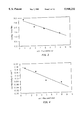
- FIG. 1 is a graph illustrating the dependence of conductivity on the type and concentration of dopant anions present in polymerizable polypyrrole-based formulations
- FIG. 2 is a graph illustrating the dependence of electrical resistance of polymerized polypyrrole films on the electron acceptor:monomer mole ratio in the starting formulation
- FIG. 3 is a graph illustrating the dependence of curing time on the concentration of initiator
- FIG. 4 is a graph illustrating the dependence of conductivity on initiator concentration
- FIG. 5 is a graph illustrating the dependence of curing time on the amount of dodecyl sulfate used as flexibilizer
- FIG. 6 is a graph illustrating the dependence of curing time and conductivity on the amount of dodecyl sulfate used as flexibilizer
- FIG. 7 is a graph illustrating the dependence of resistivity of polymerized polypyrrole films on the ratios of pyrrole:aniline monomers
- FIG. 8 is a photograph of alumina substrates with laser and electron beam patterned lines of electronically conducting polypyrrole
- FIGS. 9A and 9B contains scanning electron micrographs of the cross-sections of polypyrrole films formed electrochemically and photochemically;
- FIGS. 10A to 10D contains scanning electron micrographs of the surfaces of polypyrrole films formed electrochemically and photochemically;
- FIG. 11 is a flow chart comparing the steps of conventional PWB fabrication with those of the present invention.
- FIG. 12 is a photograph of black conducting polypyrrole lines on a fiberglass/epoxy PWB substrate patterned using UV illumination through a shadow mask, wherein one line has been electrodeposited with copper;
- FIG. 13 is a photograph of a copper-on-polypyrrole plated 0.025 inch diameter through-hole.
- FIG. 14 is a perspective view of an inductor fabricated with polymerized conducting polymers in vertical paths through a dielectric layer;
- the present invention provides a novel polymerization process for the preparation of high-quality, passive electronic elements using electronically conducting organic polymer films.
- the process utilizes a simple formulation that consists of a pure monomer (such as pyrrole or aniline), a salt and a solvent.
- Polymerization is induced allowing thin polymer patterns to be polymerized on typical PWB substrates, such as fiberglass/epoxy or polyimide, and MCM substrates, such as alumina (Al 2 O 3 ), berillia (BeO), fiberglass/epoxy, silicon, polyimide and ceramic-filled polytetrafluoroethylene.
- the formulations of the present invention may be polymerized by several methods including electrochemical, chemical, thermal, oxidation and electrolysis.
- the preferred method to polymerize a formulation which will be described in detail below, is photopolymerization.
- Direct writing of patterns in photopolymerization can be performed with an argon laser or by electron beam irradiation for improved resolution.
- a contact mask having a desired pattern inscribed therein can be placed over the substrate to block out light from undesired areas.
- the mask/board assembly is then exposed to UV (or electron beam) irradiation, promoting photopolymerization of the cast formulation (or dry film) in regions where light passes through the pattern inscribed in the mask.
- the photopolymerizable thin film formulation not exposed to the radiation can then be removed by means of an appropriate solvent.
- the formulations of the present invention include a salt that serves both as an electron acceptor for oxidation of the monomer(s) and as a dopant to preserve electroneutrality in the oxidized polymer.
- Preferred electron acceptors undergo very slow oxidation of the monomer in the dark (1-2 days) and have the highest conductivities.
- Polypyrrole (PPY) can be chemically prepared using inorganic (Fe 3+ and Cu 2+ ions) or organic (chloranil) electron acceptors.
- inorganic acceptors When inorganic acceptors are added to pyrrole-containing solutions a powdery polymer material results almost immediately after the addition. Therefore, cations having too high an oxidation potential are not suitable for photopolymerization of polypyrrole.
- organic electron acceptors Several attempts were made to use organic electron acceptors, but photopolymerization of black conductive PPY films was unsuccessful. It has been shown that electron acceptors with proper oxidation potential (e.g. Ag + , Fe 3+ or Cu 2+ ions) and dopant (e.g.
- the preferred electron acceptors are the silver salts (such as AgNO 3 , AgClO 4 and AgNO 2 ), with the most preferred being silver nitrate, AgNO 3 .
- the conductivity (or resistivity) of a polymer film can be modified by changing the molar ratio of monomer to electron acceptor over a wide range.
- FIG. 2 shows the resistance of conducting polymer films at various ratios of monomer to electron acceptor above about 0.5. Monomer/electron acceptor ratios ranging between about 2 and about 100 are preferred for producing electronically conductive polymer films.
- the electrical conductivity of the polymers decreases (resistance increases) with decreasing concentration of electron acceptor (increasing monomer to electron acceptor ratio). High electron acceptor concentrations, such as monomer/electron acceptor molar ratios below about one, have been found to produce films that are thicker than desirable.
- a polymer network can be formed by promoting the polymerization of a monomer, oligomer, or mixtures of monomers and/or oligomers.
- Polymerization is a chain reaction that can develop very rapidly, especially when intense UV radiation is used to produce the initiating species. This UV-curing reaction leads ultimately to a three-dimensional polymer network. Since most of the monomers or oligomers commonly employed do not produce initiating species with a sufficiently high yield upon UV exposure, it is preferred to introduce a photoinitiator that will allow the polymerization to start.
- a typical UV-curable formulation therefore, will contain two basic components: (i) a photoinitiator, and (ii) a monomer, oligomer, or a mixture of monomers and/or oligomers.
- photoinitiator is of prime importance in light-induced polymerizations, since it directly governs the cure rate.
- a suitable photoinitiator system must possess high absorption in the emission range of the light source.
- the photoinitiator must also form an excited state having a short lifetime to avoid quenching by oxygen or the monomer and split into reactive radicals or ionic species with the highest possible quantum yield.
- Other factors to be considered in selecting the proper photoinitiator include solubility in the monomer, storage stability and the nature of the photo-products, which should not be colored, toxic or induce some degradation of the polymer upon aging.
- Photoinitiators can be classified into three major categories, depending on the kind of mechanism involved in their photolysis: (i) radical formation by photo-cleavage; (ii) radical generation by hydrogen abstraction, and (iii) cationic photoinitiators.
- Cationic photoinitiators have proven to be particularly useful in the photopolymerization of polypyrrole from pyrrole monomers in solution. Besides their specificity, cationic-initiated photopolymerizations have the advantage of being insensitive to atmospheric oxygen. In the absence of nucleophilic reagents, the chain reaction will thus continue to develop after the illumination has ceased and provide a beneficial post-cure effect that can be enhanced by thermal treatment.
- the preferred post-photopolymerization thermal treatment involves heating the polymer at temperatures between about 80 and about 120 degrees Celsius for about three hours, with the most preferred temperature being about 100 degrees Celsius.
- Thermally stable photoinitiators for cationic polymerizations of commercial significance include the onium salts, such as triarylsulfonium and diaryliodonium, with complex metal halide anions.
- a key feature of these photoinitiators is the low nucleophilicity of the anions which reduces termination processes and allows ambient temperature cationic polymerization to proceed. The absence of air inhibition represents a distinguishing feature of cationic, as compared to radical, polymerization.
- the photoinitiators investigated include a titanocene radical photoinitiator (such as IRGACURETM 784 available from Ciba Geigy, located in Ardsley, N.Y.), a cationic ferrocinium photoinitiator (such as a (h6-benzene)(h5-cyclopentadienyl)iron(II) -hexafluorophosphate available as IRGACURETM 261 from Ciba Geigy, located in Ardsley, N.Y.), triaryl sulphonium PF 6 - salts (such as CYRACURETM 6990, available from Union Carbide, located in Danbury, Conn.), triaryl sulphonium SbF 6 - salts (such as CYRACURETM 6974, available from Union Carbide, located in Danbury, Conn.).
- the photoinitiators are preferrably added to the monomer in amounts less than about 8 weight percent, with the most preferred amounts being between about
- Photopolymerization of pyrrole alone, or pyrrole mixed with a photoinitiator such as titanocene yields a transparent yellow film exhibiting insulating properties. Resistances of over 20 M ⁇ are measured by an ohmmeter. When AgNO 3 , an electron acceptor, is dissolved into the pyrrole prior to curing, a black polymer film characteristic of conducting polypyrrole is formed.
- both electropolymerized and photopolymerized polypyrrole films suffer from poor mechanical properties. They lack flexibility, either as stand alone films or as coatings.
- Three approaches have been found to improve the mechanical properties of photopolymerized polypyrrole: (i) incorporating large amphophilic (surfactant) organic anions into the polypyrrole structure, (ii) photo-copolymerizing a suitable comonomer material with pyrrole, and (iii) including commercial flexibilizers.
- the preferred surfactants are large anionic surfactants, such as the sodium salts of dodecyl sulfate (DDS) and dodecylbenzene sulfonate (DDBS).
- the preferred comonomer is aniline.
- the preferred flexibilizer is polyethylene glycol diglycidyl ether.
- formulations can include a mixture of monomers which can be photopolymerized to form copolymers. While photo-copolymerizations can be achieved with many monomer pairings, the preferred monomer pairs for the lithographic production of an electronically conducting copolymer on a non-conducting substrate are comprised of: (i) pyrrole in combination with: (ii) a sub-stoichiometric amount of silver nitrate (such as a molar ratio of pyrrole to silver nitrate of about 8:1) and with (iii) fifteen mole percent aniline relative to pyrrole. The mixed monomer formulation is then diluted with an equivalent volume of acetonitrile to provide good contact with the substrate.
- photopolymerizable solutions are mixed in a glass vial that excludes the penetration of light.
- the solutions are then sonicated to facilitate dissolution and homogenization of the formulation. Since a slow chemical polymerization of pyrrole takes place over a period of one to two days in the presence of Ag + ions, it is preferred that fresh photopolymerizable formulations be prepared immediately prior to polymerization.
- a thin layer of the formulation is then cast and evenly spread on the surface of a selected substrate typically having a surface area of between about 1 and about 4 square centimeters (cm 2 ).
- the preferred methods of spreading the formulation over the substrate to achieve a thin layer having uniform thickness include brush coating, spraying, dipping and spin coating, with the most preferred method being spin coating.
- the oxidation process is initiated by irradiation.
- the preferred irradiation methods are those which selectively expose only discrete regions or lines on the coated substrate, such as exposure by ultraviolet light through a contact mask, direct laser imaging, or electron beam imaging. Using these methods, thin polymer patterns (lines and through-holes) are readily polymerized on various conducting and nonconducting substrates. Multiple coating-curing cycles (providing up to 10 layers) can be carried out in order to produce thick uniform films.
- Photopolymerizations according to the present invention can be accomplished with a 200-Watt mercury-xenon lamp focused through a lens vertically downward onto a circular area of less than one centimeter in diameter. All the optical accessories should be made of fused silica in order to allow high energy UV as well as visible light to pass therethrough.
- the present invention uses the radiation as the driving force to induce electron transfer from the monomer species in a cast solution film to the electron acceptor, also present in the formulation.
- the concentration of oxidized monomer increases, coupling between the oxidized monomer units begins. This process continues, resulting in growth of the conducting polymer chains. Since the polymer is oxidized, the anion present in the formulation intercalates into the polymer, maintaining electroneutrality.
- the photopolymerization process does not require a conducting substrate for deposition to take place, and conducting polymer films and/or lines of various thickness, typically between about 5 and about 300 microns can be readily photopolymerized on typical PWB substrates (e.g., fiberglass/epoxy, polyimide) and MCM (e.g., alumina) as well as on metals, ceramic, silicon, GaAs, glass, paper, TEFLON (polytetrafluoroethylene), MYLAR (polyesterfilm) and polystyrene substrates.
- PWB substrates e.g., fiberglass/epoxy, polyimide
- MCM e.g., alumina
- metals ceramic, silicon, GaAs, glass, paper, TEFLON (polytetrafluoroethylene), MYLAR (polyesterfilm) and polystyrene substrates.
- TEFLON polytetrafluoroethylene
- MYLAR polystyrene substrates.
- the photopolymerization process of the invention includes the following steps:
- the illumination induces photopolymerization of the prepolymer film at exposed areas rendering the exposed areas insoluble
- non-polymerized (non-illuminated) areas are washed off with an environmentally safe solvent (acetone) or water, leaving a pattern of conducting polymer lines.
- the main advantage of the photopolymerization process compared to electrochemical and/or chemical polymerizations, is that it allows properties of conducting polymer films to be easily designed and optimized by incorporating molecular species into the polymer structure. For example, it is possible to change the conductivity of the polymer by controlling the amount of the electron acceptor and dopant anions present in the formulations.
- the same oxidatively coupled cationic polymer is formed through photopolymerization as through electrochemical polymerization, except that the anion/monomer ratio is much higher (1:1.3) compared to that found in electrochemically formed films (1:4). This is a desirable feature because with more anions in the polymer matrix, more charge can be introduced onto the polymer chains and, consequently, higher conductivities may be achieved.
- Thermally cured polymer films either with AgNO 3 or AgTs as an electron acceptor, were of very poor quality, rough and lacked a uniform color, indicating nonhomogeneous polypyrrole films.
- Thermal curing of the first layer proceeded with incomplete coverage of the exposed substrate surface and curing resembled that of simple drying of the solution.
- photopolymerization of the first layer resulted in a completely covered substrate surface.
- curing times became longer, because of the penetration of freshly added formulation into the existing layers. Curing times for films where silver tosylate was added as the electron acceptor salt were longer than for AgNO 3 -containing samples.
- FIG. 1 shows the dependence of electrical conductivity on the concentration of electron acceptors (AgNO 3 and AgTs) added to the formulations.
- Both curves exhibit a maximum conductivity value of approximately 0.1-0.3 S cm -1 at pyrrole:salt molar ratios between about 3:1 and about 8:1. A steep decrease in conductivity occurred at molar ratios higher than 15:1.
- the conductivities were several orders of magnitude lower than those for polymer films photopolymerized with AgNO 3 .
- the data shown in FIG. 1 includes films of different thicknesses, where all of them were photopolymerized and then peeled off from Al substrates. Although the thinner films were less brittle and less fragile, no improvement in mechanical properties was observed for films photopolymerized with tosylates.
- AgNO 3 added to photopolymerizable formulations in amounts corresponding to 10-15 mol %, provide the necessary electron acceptor properties for photopolymerization to take place, and gives the amount of NO 3 - anions required for charge balance inside the polymer.
- AgNO 3 is the optimal choice of electron acceptor for the photopolymerization of pyrrole.
- Simple tests of thick film curing were performed by simultaneous illumination of formulations containing photoinitiators added at 3 wt % to an 8:1 pyrrole:AgNO 3 solution. Exposure to UV light was brought about from the top of miniature glass vials (0.7 cm dia. and 1.1 cm height) containing different photoinitiators. The process of photopolymerization was closely followed under low illumination conditions (corresponding to a temperature of 30-32° C.), in order to determine the changes taking place during photopolymerization. In all four vials the polymerization process went through different stages which affected the color of the bulk and/or surface layers of the formulations and the speed of solidification.
- ferrocinium photoinitiator is more suitable for photopolymerization of pyrrole because it allows deeper light penetration through the black solidified surface layer.
- Ferrocinium photoinitiators have been found to be successful for the photopolymerization of epoxides, which have been used in this work as potential copolymers with polypyrrole.
- FIG. 3 The effect of ferrocinium photoinitiator concentration on the curing time of PPY films is shown in FIG. 3.
- Formulations containing increasing amounts of photoinitiator were applied at different thicknesses on aluminum and glass substrates, and were cured simultaneously. Curing time was determined by observing solidification and by the pencil hardness test. Increasing the amount of photoinitiator from 1 to 8 wt % decreased the curing time by approximately a factor of two.
- FIG. 4 shows that increasing amounts of photoinitiator present in the films causes a slight decrease in conductivity.
- Organic anions tested as film flexibilizing components were DDS (dodecyl sulfate, sodium salt) and DDBS (dodecyl-benzene sulfonate, sodium salt). They were added to the already optimized formulation to yield the highest conductivity, i.e., pyrrole:AgNO 3 ratio of 8:1 and 3 wt % of IRGACURETM 261 photoinitiator. Amounts added to the formulation are expressed as pyrrole/surfactant molar ratios. Polypyrrole films were photopolymerized from these formulations under different illumination conditions and on various substrates. A post-cure thermal treatment at the highest lamp radiance was applied after photocuring. This is recommended by Ciba-Geigy for completion of curing processes when IRGACURETM 261 photoinitiator is used.
- Photopolymerization along the area of the substrate covered by the formulation was followed by observing black solidifying zones smoothly spreading across the surface of the substrate. It was evident that these additives helped diffusion of polymerizing components in the thin formulation layer. Curing was generally slower than for the films without surfactant additives. Films obtained showed a significant improvement in mechanical properties. They were very flexible compared to the films that did not contain surfactant additives. It was possible to bend these films, whether coated on an aluminum sheet or on polystyrene, through angles greater than 90° without breaking them. Additives acting as surfactants greatly improved the adherence of the film to the substrate. More importantly, films so formulated retained good conductivity.
- DDBS was less soluble in pyrrole and gave rise to films of lower flexibility when compared to films with DDS as an additive.
- Table 3 compares conductivities for DDS- and DDBS-containing films, added as pyrrole:surfactant molar ratios of 15:1.
- FIGS. 5 and 6 show variations in curing time and conductivity of films photopolymerized with different concentrations of DDS additive. It was possible to follow the curing progress at two stages: corresponding to surface solidification and when curing was completed. Both plots exhibit the same slope, showing that the curing time is longer with increasing amounts of DDS in the films. Films with higher concentrations of surfactant additive became soft. The electrical conductivity of the films was within the range 0.1-0.5 S cm -1 . Minimum electrical conductivity, evident at ratios between 30:1 to 50:1, is probably due to an artifact in that the resistivity probe tips penetrated into the soft films at ratios greater than 30:1 and hence, displayed conductivity values higher than those for the films of measured thickness. It was found that films containing between 10:1 and 20:1 of pyrrole:DDS additive, possess the greatest flexibility and conductivity.
- Example 5 A series of experiments were performed under the conditions described in Example 5, for various copolymer materials such as an aqueous acrylic resin, bisphenol A diglycidyl ether, and perfluorinated sulfonic acid. The results are given below in Table 4.
- the waterborne acrylic resin did not undergo successful copolymerization with pyrrole. It was possible to make a film only if it was added at amounts less than 4 wt %, however, resulting in reduced conductivity. Acrylic resins undergo very little cationic polymerization (mostly radical induced), which is incompatible with the photo-polymerization of pyrrole.
- Copolymerization of pyrrole with bisphenol A diglycidyl ether which undergoes a cationic photopolymerization mechanism, resulted in good films covering a large range of pyrrole/copolymer ratios from 10:1 to 1:1. It may be noted that on using the ferrocinium photoinitiator and bisphenol A diglycidyl ether alone, a yellow nonconducting film was obtained. Conductivities of PPY/epoxide copolymers were approximately an order of magnitude lower than that of PPY films without a copolymer. Increasing the amount of epoxy copolymer up to a ratio of 1:1 resulted in an order of magnitude decrease in conductivity as shown in Table 4.
- PPY/epoxide copolymers possessed good flexibility and exhibited softness, the latter increasing when higher amounts of epoxide copolymer were added. Also, these films adhered very well to metallic and nonmetallic substrates, and it was difficult to peel them off, partly due to their softness.
- a test was performed using a high resolution laser and an electron-beam for the patterning of conducting polypyrrole lines.
- alumina substrates (bottom row, one inch by one inch substrates), have laser patterned lines formed from a 4:1 pyrrole:silver nitrate formulation spun at 500, 300, and 1000 RPM, respectively. Each alumina substrate contains several sets of 3-5 lines obtained with a different number of laser beam passes. Alumina substrates shown in the top row (one inch by one inch substrates) have laser patterned lines using an 8:1 pyrrole:silver nitrate formulation spun at 500 and 1000 RPM, respectively. The small alumina substrate has a patterned line formed from a 4:1 pyrrole:silver nitrate formulation photopolymerized by a 10 nm wide electron beam. Each of the formulations contained acetonitrile.
- An electron beam was used to fabricate both narrow lines (down to 1.5 microns wide) and wide lines (about 80 microns wide) (See FIG. 8), using the same exposure parameters, but two different techniques.
- the narrow lines were fabricated using a step and repeat technique, (i.e. the electron beam was moved across the sample and the sample moved between exposures) to form a number of parallel lines with approximately equal line widths and spacing.
- the wide lines were fabricated by exposing narrow lines together (side by side), with sufficient overlap to eliminate any visible rastering under SEM examination.
- FIGS. 9A and 9B Scanning electron micrographs of fracture surfaces of thick photopolymerized (70 microns) and electropolymerized (67 microns) polypyrrole films are shown in FIGS. 9A and 9B. It can be seen from FIG. 9A that electrochemically prepared polypyrrole is dense, non-fibrillar and volume-filling. The photopolymerized polypyrrole material of FIG. 9B is surprisingly compact, but more open-structured and contains some voids.
- FIGS. 10A and 10B Scanning electron micrographs at two magnifications of the outer surfaces of electropolymerized and photopolymerized polypyrrole films are presented in FIGS. 10A and 10B.
- an electrochemically prepared polypyrrole is shown to have nodular or "cauliflower" structures that are consistent with a nucleation/dendritic film growth mechanism. This surface topology is frequently observed for electrochemically prepared polypyrrole materials.
- the surface topography for the photopolymerized polypyrrole films shown in FIGS. 10B and 10D was rather featureless, being smooth and flat. As is observed in the micrograph of the fractured surface of photopolymerized PPY in FIG.
- the resistivity of electronically conducting polymer lines can be controlled by the concentration or type of dopant anions from an electron acceptor salt (See FIGS. 1 and 2) or the concentration and type of copolymers present in the starting formulation (See FIG. 7).
- concentration or type of dopant anions from an electron acceptor salt See FIGS. 1 and 2
- concentration and type of copolymers present in the starting formulation See FIG. 7.
- the pyrrole:comonomer ratio in the formulation particularly the pyrrole:aniline ratio
- the preferred copolymer is aniline and the prefered pyrrole:aniline mole ratios are between about 1 and about 100.
- concentration of electron acceptor salts including the dopant anions in the formulation be used to determine the approximate resistivity of the electronically conducting polymer lines produced upon photopolymerization of the formulation.
- the overall resistivity of an electronically conducting polymer resistor is a function of the resistivity of the photopolymerized formulation as well as the thickness, width and length of the resistor.
- a plurality of resistors can be formed on a common substrate, where the resistors have various overall resistances on the order of about 10 ohms ( ⁇ ) to about 10 M ⁇ .
- One preferred method for forming resistors with various resistances in a single layer on a substrate involves the preparation of a plurality of formulations having different concentrations of the electron acceptor salt. Each formulation can be used to form resistors having resistances within a certain range. Increasing the electron acceptor salt concentration, such as AgNO 3 , increases the conductivity and decreases the resistivity of the photopolymerized conducting polymer.
- a first formulation might be used to form about 10-100 ⁇ resistors and two more formulations might be used to form about 100-10,000 ⁇ and about 10K ⁇ -10 M ⁇ resistors, respectively. Only one formulation is applied, dried and photopolymerized at a time. Each individual formulation is spin-coated onto the substrate to form a film having substantially uniform thickness. After allowing time for the formulation to dry, select areas or lines are photopolymerized using any of the techniques previously described, e.g., masked UV light, laser light, or electron beams. The unpolymerized formulation is then washed from the substrate surface by a suitable solvent. Since the thickness of the resistor lines are substantially uniform, due to the spin-coating, of the formulation, and the length of the resistor must span between two conductor contact points, it is preferred that the width of the resistor be varied to achieve a desired resistance.
- each resistor be established by photopolymerizing resistor lines having a width that will form the desired resistance.
- the photopolymerization process may form lines having sides that are not entirely uniform or smooth, it may be difficult to obtain resistors having resistances within narrow tolerances without further processing.
- the overall resistance of a resistor may be increased by reducing the width of the resistor line through laser trimming. Therefore, in applications where a precise resistance is necessary or desirable, it is preferred to photopolymerize a resistor line having a width slightly greater than is needed to achieve the desired resistance, thereby forming a resistor having a resistance lower than desired, and then trim the width of the resistor with a laser until the resistance increases to the desired value.
- resistors having resistances within the first formulation's useful range After all the resistors having resistances within the first formulation's useful range have been formed, additional formulations may be used to obtain resistors within other ranges. Any number of formulations may be applied in this manner having wide or narrow resistance ranges.
- the preferred method of forming a plurality of resistors having various resistances involves spin-coating, drying, photopolymerizing and washing a first formulation, then repeating these steps for each remaining formulation. Only after all resistors have been photopolymerized will they receive a single thermal cure and each of the resistors, regardless of formulation, will be laser trimmed to a specific resistance.
- solid electrolytic capacitors in which an electronically conducting polymer is applied as an electrolyte, could be fabricated that would exhibit good frequency and thermal stability characteristics.
- the conducting polymers could be photopolymerized on the surface of dielectric materials, such as etched or anodized aluminum and tantalum, to form a solid state electrolytic capacitor in which a conductive polymer is applied as an electrolyte.
- a process for forming a solid state electrolytic capacitor might comprise the steps of applying a thin film of a formulation on a dielectric layer; photopolymerizing a portion of the film; removing the unpolymerized portion of the film from the substrate with a solvent; depositing a layer of palladium onto the surface of photopolymerized polymer by immersion in solution consisting of a palladium containing salt; and electrodepositing a layer of a metal conductor such as gold, copper or platinum on palladium precoat.
- a metal conductor such as gold, copper or platinum on palladium precoat.
- the preferred method of forming three-dimensional inductors comprises the steps of: (i) photopolymerizing a conducting polymer on a substrate with subsequent metallization, (ii) deposition of a dielectric layer whether by photopolymerization or other means, (iii) drilling holes (on the order of about 250 ⁇ m and smaller) in the dielectric layer by laser ablation, (iv) simultaneous photopolymerization of the through-holes and conducting lines on the top of the dielectric layer, and (v) metalization of the conducting polymer vias (both through-holes and conducting lines.
- the deposition of conducting polymers on through-hole walls can be achieved by coating the walls with a layer of photopolymerizable material (See FIG. 13), preferably in the same step that the material is coated on the top surface of the dielectric material. It is also preferred that the photopolymerization of the through-holes and conducting polymers on the top surface be carried out simultaneously.
- Spontaneous deposition of noble metals e.g. palladium (Pd) and silver (Ag) onto polypyrrole occurs simply by immersing the substrate in an aqueous solution containing the corresponding metal salt. It may also be possible to spontaneously deposit gold (Au), and other metals on photopolymerized polypyrrole.
- the preferred noble metal is palladium. While palladium may be used with any Pd 2+ salt, (i.e. PdBr 2 , PdCl 2 ) the most preferred metal salt is palladium bromide.
- the methods of the present invention may be used alone or in combination with other technology for forming multichip modules.
- the passive elements of the present invention may be incorporated into integrated circuits formed primarily using thin film or thick film technologies.
- a specific circuit may be optimized by using a resistor according to the present invention.
- the remainder of the integrated circuit, including logic elements, conductive lines and the like, may be formed on a substrate using chemical vapor deposition (CVD) and physical vapor deposition (PVD).
- CVD chemical vapor deposition
- PVD physical vapor deposition
- the integrated circuit is formed layer by layer until the resistor is needed.
- the underlying layer will preferrably provide a pair of conductive leads on which the resistor is formed.
- the surface of the substrate may be planarized and the resistor covered by conventional dielectric chemical vapor deposition (DCVD). Formation of integrated circuits may continue on the same or subsequent layers.
- DCVD dielectric chemical vapor deposition
Abstract
Description
                                  TABLE 1
__________________________________________________________________________
Comparison of photopolymerized and thermally polymerized polypyrrole
films
(pyrrole/electron acceptor molar ratio was 50:1; photoinitiator: 3 wt %
IRGACURE ™ 261)
              AgNO.sub.3      AgTs
LAYER
     ELECTRON PHOTO-  THERMALLY
                              PHOTO-  THERMALLY
NUMBER
     ACCEPTOR POLYMERIZED
                      POLYMERIZED
                              POLYMERIZED
                                      POLYMERIZED
__________________________________________________________________________
FIRST
     CURE     68      69      68      69
LAYER
     TEMPERATURE
     °C.
     CURING TIME
               2       3.5     3      18
     min
     POLYMER FILM
              smooth, incomplete
                              smooth, green-
                                      incomplete
     APPEARANCE
              black, brittle
                      coverage,
                              black, brittle
                                      coverage,
                      gray-black,     gray-green black,
                      rough, brittle  rough, brittle
FIFTH
     CONDUCTIVITY
               9.7 × 10.sup.-3
                       3.8 × 10.sup.-2
                               4.1 × 10.sup.-4
                                       6.0 × 10.sup.-5
LAYER
     S cm.sup.-1
     CURE     68      68      67      68
     TEMPERATURE
     °C.
     CURING TIME
               7       8       9      20
     min
     POLYMER FILM
              smooth, gray-white-black,
                              smooth, green-
                                      gray-white-black,
     APPEARANCE
              black, brittle
                      rough, brittle
                              black, brittle
                                      rough, brittle
__________________________________________________________________________
                                  TABLE 2
__________________________________________________________________________
Conductivity of photopolymerized PPY films containing different anions
(electron acceptor: Ag.sup.+ ; photoinitiator: 3 wt % IRGACURE ™ 261;
pyrrole/salt ratio = 8:1).
ELECTRON
       STAND ALONE FILMS
                       FILMS ON POLYSTYRENE
ACCEPTOR
       CONDUCTIVITY
                THICKNESS
                       CONDUCTIVITY
                                THICKNESS
SALT   S cm.sup.-1
                μm  S cm.sup.-1
                                μm
__________________________________________________________________________
AgNO.sub.3
       0.425    62     0.158    34
AgTs   0.197    88     0.179    53
AgBF.sub.4             0.0018   57
AgNO.sub.3 /AgTs
       0.212    168
AgNO.sub.3 /AgBF.sub.4
       0.375    51
__________________________________________________________________________
                                  TABLE 3
__________________________________________________________________________
Conductivity of photopolymerized PPY films with large organic anions as
flexibilizers (polypyrrole/AgNO.sub.3 = 8:1; polypyrrole/surfactant =
15:1;
photoinitiator: 3 wt % IRGACURE ™ 261;
curing time: fast, 1.9 W cm.sup.-2 with thermal post-cure: 2.3 W
cm.sup.-2).
ADDITIVE DDS             DDBS
SUBSTRATE
         CONDUCTIVITY
                  THICKNESS
                         CONDUCTIVITY
                                  THICKNESS
MATERIAL S cm.sup.-1
                  μm  S cm.sup.-1
                                  μm
__________________________________________________________________________
STAND ALONE
         0.21     163    0.20     215
STAND ALONE
         0.51     61     0.59     75
STAND ALONE
         0.134    224
PPY/AgNO.sub.3 = 5/1
POLYSTYRENE
         0.48     39     0.32     62
POLYMER FILM
         smooth, black,  smooth, black,
APPEARANCE
         curing time: 1.3 min/layer,
                         curing time: 2 min/layer,
         very flexible   flexible
__________________________________________________________________________
                                  TABLE 4
__________________________________________________________________________
Conductivity of PPY films photo-copolymerized with different resins
(pyrrole/
AgNO.sub.3 = 8:1; photoinitiator: 3 wt % IRGACURE ™ 261; curing:
different conditions; average
1.2 W cm.sup.-2 ; for ARALDITE (epoxyresin available from Electron
Microscopy Sciences of
Fort Washington, PA.) 2.1 W cm.sup.-2 and thermal postcure at 2.3 W
cm.sup.-2).
COPOLYMER
        % (w/w)  THICKNESS
                        CONDUCTIVITY
MATERIAL
        OF COPOLYMER
                 μm  S cm.sup.-1
                                 COMMENT
__________________________________________________________________________
MAINCOTE
        50                       no polym., yellow precipitate
HG 54 D (1:1)
MAINCOTE
        4        65     0.074    black
HG 54 D
MAINCOTE
        4        119    0.072    "
HG 54 D
ARALDITE
        10       121    0.086    black, smooth, flexible
502     14       74     0.022    longer curing needed
polystyrene
        20       159    0.0092   at high lamp power
(on glass)
        14       41     0.063    t > 10-15 min/layer
        20       20     0.044    "
        34       14     0.015    "
        51       12     0.0068   "
NAFION  5        64     0.53     black, smooth, flexible
        10                       too resistive, voltage transients
                                 show saturation
__________________________________________________________________________
Claims (66)
Priority Applications (1)
| Application Number | Priority Date | Filing Date | Title |
|---|---|---|---|
| US08/881,107 US5948232A (en) | 1995-06-19 | 1997-06-23 | Method of manufacturing passive elements using conductive polypyrrole formulations |
Applications Claiming Priority (4)
| Application Number | Priority Date | Filing Date | Title |
|---|---|---|---|
| US08/492,235 US6210537B1 (en) | 1995-06-19 | 1995-06-19 | Method of forming electronically conducting polymers on conducting and nonconducting substrates |
| US08/491,625 US5545308A (en) | 1995-06-19 | 1995-06-19 | Method of using conductive polymers to manufacture printed circuit boards |
| US08/630,063 US5855755A (en) | 1995-06-19 | 1996-04-12 | Method of manufacturing passive elements using conductive polypyrrole formulations |
| US08/881,107 US5948232A (en) | 1995-06-19 | 1997-06-23 | Method of manufacturing passive elements using conductive polypyrrole formulations |
Related Parent Applications (1)
| Application Number | Title | Priority Date | Filing Date |
|---|---|---|---|
| US08/630,063 Continuation-In-Part US5855755A (en) | 1995-06-19 | 1996-04-12 | Method of manufacturing passive elements using conductive polypyrrole formulations |
Publications (1)
| Publication Number | Publication Date |
|---|---|
| US5948232A true US5948232A (en) | 1999-09-07 |
Family
ID=27413907
Family Applications (1)
| Application Number | Title | Priority Date | Filing Date |
|---|---|---|---|
| US08/881,107 Expired - Fee Related US5948232A (en) | 1995-06-19 | 1997-06-23 | Method of manufacturing passive elements using conductive polypyrrole formulations |
Country Status (1)
| Country | Link |
|---|---|
| US (1) | US5948232A (en) |
Cited By (10)
| Publication number | Priority date | Publication date | Assignee | Title |
|---|---|---|---|---|
| US6111685A (en) * | 1997-12-19 | 2000-08-29 | Rockwell Science Center, Llc | Reversible electrochemical mirror (REM) with improved electrolytic solution |
| US6400491B1 (en) * | 1997-12-19 | 2002-06-04 | Innovative Technology Licensing, Llc | Fast-switching reversible electrochemical mirror (REM) |
| US20030166831A1 (en) * | 2001-06-25 | 2003-09-04 | Massachusetts Institute Of Technology | Bioerodible conducting materials |
| US6737287B1 (en) * | 1999-02-17 | 2004-05-18 | Canon Kabushiki Kaisha | Ink used for ink jet, and methods for manufacturing conductive film, electron-emitting device, electron source and image-forming apparatus |
| US20050092612A1 (en) * | 2003-06-23 | 2005-05-05 | Canon Kabushiki Kaisha | Electrodeposition film forming method, and semiconductor apparatus |
| US20060118922A1 (en) * | 2002-10-31 | 2006-06-08 | Goodner Michael D | Selectively growing a polymeric material on a semiconductor substrate |
| US9586070B2 (en) | 2013-01-22 | 2017-03-07 | Miraculum, Inc. | Flame retardant and fire extinguishing product for fires in solid materials |
| US9597538B2 (en) | 2013-01-22 | 2017-03-21 | Miraculum, Inc. | Flame retardant and fire extinguishing product for fires in liquids |
| WO2018220072A1 (en) * | 2017-06-01 | 2018-12-06 | Mycronic AB | Method and system for manufacturing a workpiece by providing for a tackiness of a mixture of material adapted to modify its electrical conductivity when exposed with electromagnetic radiation |
| US20190109000A1 (en) * | 2017-10-11 | 2019-04-11 | Lawrence Livermore National Security, Llc | Localized electron beam induced deposition of silicon carbide |
Citations (5)
| Publication number | Priority date | Publication date | Assignee | Title |
|---|---|---|---|---|
| JPH01123228A (en) * | 1987-11-09 | 1989-05-16 | Res Dev Corp Of Japan | Method for forming pattern of conductive high polymer by photopolymerization |
| US5127989A (en) * | 1990-05-18 | 1992-07-07 | Kabushiki Kaisha Toshiba | Method of forming a thin film pattern with a trapezoidal cross section |
| EP0495549A2 (en) * | 1991-01-17 | 1992-07-22 | Dsm N.V. | Process for preparing polymers and moulding compounds based thereon |
| WO1994002886A1 (en) * | 1992-07-15 | 1994-02-03 | Dsm N.V. | Method for the preparation of a polymer composition containing an electrically conductive polymer |
| US5545308A (en) * | 1995-06-19 | 1996-08-13 | Lynntech, Inc. | Method of using conductive polymers to manufacture printed circuit boards |
-
1997
- 1997-06-23 US US08/881,107 patent/US5948232A/en not_active Expired - Fee Related
Patent Citations (5)
| Publication number | Priority date | Publication date | Assignee | Title |
|---|---|---|---|---|
| JPH01123228A (en) * | 1987-11-09 | 1989-05-16 | Res Dev Corp Of Japan | Method for forming pattern of conductive high polymer by photopolymerization |
| US5127989A (en) * | 1990-05-18 | 1992-07-07 | Kabushiki Kaisha Toshiba | Method of forming a thin film pattern with a trapezoidal cross section |
| EP0495549A2 (en) * | 1991-01-17 | 1992-07-22 | Dsm N.V. | Process for preparing polymers and moulding compounds based thereon |
| WO1994002886A1 (en) * | 1992-07-15 | 1994-02-03 | Dsm N.V. | Method for the preparation of a polymer composition containing an electrically conductive polymer |
| US5545308A (en) * | 1995-06-19 | 1996-08-13 | Lynntech, Inc. | Method of using conductive polymers to manufacture printed circuit boards |
Non-Patent Citations (6)
| Title |
|---|
| Kern et al., Photochemical Deposition of Electrically Conducting Polypyrrole, J. Chem. Soc. Chem. Commun., pp. 657 658, no month available/1989. * |
| Kern et al., Photochemical Deposition of Electrically Conducting Polypyrrole, J. Chem. Soc. Chem. Commun., pp. 657-658, no month available/1989. |
| Park, Yamamoto, Takeoka and Tsuchida; "Simultaneous Formation of a Polypyrrole Film and a Tantalum OxideLayer by Electrochemical Oxidation"; 1992 The Chemical Society of Japan; pp. 1860-1865 no month available. |
| Park, Yamamoto, Takeoka and Tsuchida; Simultaneous Formation of a Polypyrrole Film and a Tantalum OxideLayer by Electrochemical Oxidation ; 1992 The Chemical Society of Japan; pp. 1860 1865 no month available. * |
| Yoneyama et al., Photocatalytic Deposition of Light Localized Polypyrrole Film Pattern on N Type Silicon Wafer, Chem Let., pp. 657 660, 1986. * |
| Yoneyama et al., Photocatalytic Deposition of Light-Localized Polypyrrole Film Pattern on N-Type Silicon Wafer, Chem Let., pp. 657-660, 1986. |
Cited By (15)
| Publication number | Priority date | Publication date | Assignee | Title |
|---|---|---|---|---|
| US6400491B1 (en) * | 1997-12-19 | 2002-06-04 | Innovative Technology Licensing, Llc | Fast-switching reversible electrochemical mirror (REM) |
| US6111685A (en) * | 1997-12-19 | 2000-08-29 | Rockwell Science Center, Llc | Reversible electrochemical mirror (REM) with improved electrolytic solution |
| US6737287B1 (en) * | 1999-02-17 | 2004-05-18 | Canon Kabushiki Kaisha | Ink used for ink jet, and methods for manufacturing conductive film, electron-emitting device, electron source and image-forming apparatus |
| WO2001006312A1 (en) * | 1999-07-19 | 2001-01-25 | Rockwell Science Center, Llc | Reversible electrochemical mirror (rem) with improved electrolytic solution |
| US20030166831A1 (en) * | 2001-06-25 | 2003-09-04 | Massachusetts Institute Of Technology | Bioerodible conducting materials |
| US7291693B2 (en) | 2001-06-25 | 2007-11-06 | Massachusetts Institute Of Technology | Bioerodible conducting materials |
| US20060118922A1 (en) * | 2002-10-31 | 2006-06-08 | Goodner Michael D | Selectively growing a polymeric material on a semiconductor substrate |
| US7052991B2 (en) * | 2003-06-23 | 2006-05-30 | Canon Kabushiki Kaisha | Electrodeposition film forming method, and semiconductor apparatus |
| US20050092612A1 (en) * | 2003-06-23 | 2005-05-05 | Canon Kabushiki Kaisha | Electrodeposition film forming method, and semiconductor apparatus |
| US9586070B2 (en) | 2013-01-22 | 2017-03-07 | Miraculum, Inc. | Flame retardant and fire extinguishing product for fires in solid materials |
| US9597538B2 (en) | 2013-01-22 | 2017-03-21 | Miraculum, Inc. | Flame retardant and fire extinguishing product for fires in liquids |
| US9878190B2 (en) | 2013-01-22 | 2018-01-30 | Miraculum, Inc. | Flame retardant and fire extinguishing product for fires in solid materials |
| WO2018220072A1 (en) * | 2017-06-01 | 2018-12-06 | Mycronic AB | Method and system for manufacturing a workpiece by providing for a tackiness of a mixture of material adapted to modify its electrical conductivity when exposed with electromagnetic radiation |
| US20190109000A1 (en) * | 2017-10-11 | 2019-04-11 | Lawrence Livermore National Security, Llc | Localized electron beam induced deposition of silicon carbide |
| US10395923B2 (en) * | 2017-10-11 | 2019-08-27 | Lawrence Livermore National Security, Llc | Localized electron beam induced deposition of silicon carbide |
Similar Documents
| Publication | Publication Date | Title |
|---|---|---|
| US5855755A (en) | Method of manufacturing passive elements using conductive polypyrrole formulations | |
| US6210537B1 (en) | Method of forming electronically conducting polymers on conducting and nonconducting substrates | |
| US5545308A (en) | Method of using conductive polymers to manufacture printed circuit boards | |
| US5427841A (en) | Laminated structure of a metal layer on a conductive polymer layer and method of manufacturing such a structure | |
| US6709806B2 (en) | Method of forming composite member | |
| JP3530565B2 (en) | Method of producing conductive polymer pattern on substrate surface and method of metallizing such pattern | |
| EP1007349B1 (en) | Patterned conducting polymer surfaces and process for preparing the same and devices containing the same | |
| US8216503B2 (en) | Method for manufacturing printed circuit board using imprinting | |
| US5948232A (en) | Method of manufacturing passive elements using conductive polypyrrole formulations | |
| JP3766288B2 (en) | Composite member manufacturing method and electronic package | |
| EP1088121A2 (en) | Method for metal coating of substrates | |
| US5885711A (en) | Electrically conductive polymer compositions, production process and coated substrates | |
| Popall et al. | ORMOCER® S–Inorganic-organic hybrid materials for e/o-interconnection-technology | |
| EP0615257A2 (en) | Laminated structure of a metal layer on a conductive polymer layer and method of manufacturing such a structure | |
| WO2009080642A2 (en) | Process for manufacturing conductive tracks | |
| US6334965B1 (en) | Electronically conductive polymers | |
| TW200938601A (en) | Process for the preparation of coatings exhibiting increased conductivity based on polythiophene and its derivatives | |
| JP4314236B2 (en) | Method for manufacturing composite member, photosensitive composition, insulator for manufacturing composite member, composite member, multilayer wiring board, and electronic package | |
| US5045159A (en) | Derivatives of compounds containing a carbonyl group conjugated to an aromatic moiety and electrophilic methods of fabrication thereof | |
| JPH11246822A (en) | Polyaniline solution containing bicyclic terperne solvent | |
| US5859085A (en) | Stable powders made from photosensitive polycrystalline complexes of heterocyclic monomers and their polymers | |
| KR930010613A (en) | How to Form Solder Mask | |
| JPH06102718B2 (en) | Method for producing polypyrrole gel | |
| WO1994002886A1 (en) | Method for the preparation of a polymer composition containing an electrically conductive polymer | |
| JP2000191822A (en) | Porous polymer thin film and semiconductor device |
Legal Events
| Date | Code | Title | Description |
|---|---|---|---|
| AS | Assignment |
Owner name: LYNNTECH, INC., TEXAS Free format text: ASSIGNMENT OF ASSIGNORS INTEREST;ASSIGNORS:MURPHY, OLIVER M.;HITCHENS, G. DUNCAN;CLARKE, ERIC T.;AND OTHERS;REEL/FRAME:009090/0425;SIGNING DATES FROM 19971201 TO 19971205 |
|
| FEPP | Fee payment procedure |
Free format text: PAT HOLDER CLAIMS SMALL ENTITY STATUS, ENTITY STATUS SET TO SMALL (ORIGINAL EVENT CODE: LTOS); ENTITY STATUS OF PATENT OWNER: SMALL ENTITY |
|
| REFU | Refund |
Free format text: REFUND - PAYMENT OF MAINTENANCE FEE, 4TH YEAR, LARGE ENTITY (ORIGINAL EVENT CODE: R1551); ENTITY STATUS OF PATENT OWNER: SMALL ENTITY |
|
| FPAY | Fee payment |
Year of fee payment: 4 |
|
| AS | Assignment |
Owner name: AIR FORCE, UNITED STATES, NEW MEXICO Free format text: CONFIRMATORY LICENSE;ASSIGNOR:LYNNTECH, INC., F2601-94-C-0097;REEL/FRAME:017879/0101 Effective date: 20050913 |
|
| FPAY | Fee payment |
Year of fee payment: 8 |
|
| AS | Assignment |
Owner name: CITY BANK, TEXAS Free format text: SECURITY AGREEMENT;ASSIGNOR:LYNNTECH, INC.;REEL/FRAME:019035/0928 Effective date: 20070309 |
|
| REMI | Maintenance fee reminder mailed | ||
| LAPS | Lapse for failure to pay maintenance fees | ||
| STCH | Information on status: patent discontinuation |
Free format text: PATENT EXPIRED DUE TO NONPAYMENT OF MAINTENANCE FEES UNDER 37 CFR 1.362 |
|
| FP | Lapsed due to failure to pay maintenance fee |
Effective date: 20110907 |