US5902703A - Method for measuring dimensional anomalies in photolithographed integrated circuits using overlay metrology, and masks therefor - Google Patents
Method for measuring dimensional anomalies in photolithographed integrated circuits using overlay metrology, and masks therefor Download PDFInfo
- Publication number
- US5902703A US5902703A US08/826,482 US82648297A US5902703A US 5902703 A US5902703 A US 5902703A US 82648297 A US82648297 A US 82648297A US 5902703 A US5902703 A US 5902703A
- Authority
- US
- United States
- Prior art keywords
- circuit features
- width
- formation
- mask
- semiconductor wafer
- Prior art date
- Legal status (The legal status is an assumption and is not a legal conclusion. Google has not performed a legal analysis and makes no representation as to the accuracy of the status listed.)
- Expired - Fee Related
Links
Images


Classifications
-
- G—PHYSICS
- G03—PHOTOGRAPHY; CINEMATOGRAPHY; ANALOGOUS TECHNIQUES USING WAVES OTHER THAN OPTICAL WAVES; ELECTROGRAPHY; HOLOGRAPHY
- G03F—PHOTOMECHANICAL PRODUCTION OF TEXTURED OR PATTERNED SURFACES, e.g. FOR PRINTING, FOR PROCESSING OF SEMICONDUCTOR DEVICES; MATERIALS THEREFOR; ORIGINALS THEREFOR; APPARATUS SPECIALLY ADAPTED THEREFOR
- G03F7/00—Photomechanical, e.g. photolithographic, production of textured or patterned surfaces, e.g. printing surfaces; Materials therefor, e.g. comprising photoresists; Apparatus specially adapted therefor
- G03F7/70—Microphotolithographic exposure; Apparatus therefor
- G03F7/70483—Information management; Active and passive control; Testing; Wafer monitoring, e.g. pattern monitoring
- G03F7/70605—Workpiece metrology
- G03F7/70616—Monitoring the printed patterns
-
- G—PHYSICS
- G03—PHOTOGRAPHY; CINEMATOGRAPHY; ANALOGOUS TECHNIQUES USING WAVES OTHER THAN OPTICAL WAVES; ELECTROGRAPHY; HOLOGRAPHY
- G03F—PHOTOMECHANICAL PRODUCTION OF TEXTURED OR PATTERNED SURFACES, e.g. FOR PRINTING, FOR PROCESSING OF SEMICONDUCTOR DEVICES; MATERIALS THEREFOR; ORIGINALS THEREFOR; APPARATUS SPECIALLY ADAPTED THEREFOR
- G03F7/00—Photomechanical, e.g. photolithographic, production of textured or patterned surfaces, e.g. printing surfaces; Materials therefor, e.g. comprising photoresists; Apparatus specially adapted therefor
- G03F7/70—Microphotolithographic exposure; Apparatus therefor
- G03F7/70425—Imaging strategies, e.g. for increasing throughput or resolution, printing product fields larger than the image field or compensating lithography- or non-lithography errors, e.g. proximity correction, mix-and-match, stitching or double patterning
- G03F7/70433—Layout for increasing efficiency or for compensating imaging errors, e.g. layout of exposure fields for reducing focus errors; Use of mask features for increasing efficiency or for compensating imaging errors
- G03F7/70441—Optical proximity correction [OPC]
-
- G—PHYSICS
- G03—PHOTOGRAPHY; CINEMATOGRAPHY; ANALOGOUS TECHNIQUES USING WAVES OTHER THAN OPTICAL WAVES; ELECTROGRAPHY; HOLOGRAPHY
- G03F—PHOTOMECHANICAL PRODUCTION OF TEXTURED OR PATTERNED SURFACES, e.g. FOR PRINTING, FOR PROCESSING OF SEMICONDUCTOR DEVICES; MATERIALS THEREFOR; ORIGINALS THEREFOR; APPARATUS SPECIALLY ADAPTED THEREFOR
- G03F7/00—Photomechanical, e.g. photolithographic, production of textured or patterned surfaces, e.g. printing surfaces; Materials therefor, e.g. comprising photoresists; Apparatus specially adapted therefor
- G03F7/70—Microphotolithographic exposure; Apparatus therefor
- G03F7/70483—Information management; Active and passive control; Testing; Wafer monitoring, e.g. pattern monitoring
- G03F7/70605—Workpiece metrology
- G03F7/70616—Monitoring the printed patterns
- G03F7/70633—Overlay, i.e. relative alignment between patterns printed by separate exposures in different layers, or in the same layer in multiple exposures or stitching
-
- G—PHYSICS
- G03—PHOTOGRAPHY; CINEMATOGRAPHY; ANALOGOUS TECHNIQUES USING WAVES OTHER THAN OPTICAL WAVES; ELECTROGRAPHY; HOLOGRAPHY
- G03F—PHOTOMECHANICAL PRODUCTION OF TEXTURED OR PATTERNED SURFACES, e.g. FOR PRINTING, FOR PROCESSING OF SEMICONDUCTOR DEVICES; MATERIALS THEREFOR; ORIGINALS THEREFOR; APPARATUS SPECIALLY ADAPTED THEREFOR
- G03F7/00—Photomechanical, e.g. photolithographic, production of textured or patterned surfaces, e.g. printing surfaces; Materials therefor, e.g. comprising photoresists; Apparatus specially adapted therefor
- G03F7/70—Microphotolithographic exposure; Apparatus therefor
- G03F7/70483—Information management; Active and passive control; Testing; Wafer monitoring, e.g. pattern monitoring
- G03F7/70605—Workpiece metrology
- G03F7/70616—Monitoring the printed patterns
- G03F7/70641—Focus
Definitions
- This invention relates generally to the field of fabricating integrated circuits and more particularly to maintaining accuracy in the fabrication of such circuits having relatively long and extremely narrow line elements such as gates.
- the invention is also directed to the verification of stepper lens fabrication quality.
- each element is ordinarily produced by a lithographic process wherein an image of one or several of the individual circuit elements or features is projected onto the wafer at a time. Because of the small size of such elements and the importance of their being accurately sized and positioned, the fabrication equipment is frequently checked for a number of possible dimensional anomalies and aberrations. These checks include "best focus" at the center of the lens for both the x and y directions as well as the "best focus” at a number of locations displaced from the center, again for both the x and y directions. Likewise, it is checked for coma (comatic aberration) and other aberrations. Such aberrations are well known in the art. See, for instance, E. HECHT, OPTICS (2d ed. reprinted with corrections 1990) p.223 or OPTICAL SOCIETY of AMERICA, HANDBOOK OF OPTICS Vol. II (2d ed. 1995) Chapter 1.
- the usual way at the present time for making such checks and measuring discrepancies is with a traditional box in a box configuration having an outside box of about 20 ⁇ m square defined by a line or trench and a centrally disposed inside box of about 10 ⁇ m square similarly defined by a line or trench.
- one of the boxes is formed as a solid square rather than merely a line configuration.
- the boxes need not be limited to clear tone patterns but could be formed of a dark tone.
- the square in a square configuration utilizes a measurement between edges of the two squares. Such measurements can be taken with the aid of a scanning electronic microscope (SEM) and can be very accurate when measuring relatively large areas or verifying the position and dimensions of relatively large features. Even so, they may be quite time consuming since only about 40 individual measurements can be completed per hour.
- SEM scanning electronic microscope
- the shortening effect is increased when the projection is out of focus, thereby causing more light scatter. Consequently, the focus throughout the entire field of the projection must be considered.
- the length of the line may be reduced by coma and this aberration is also carefully monitored. In such cases, the accuracy of the lens projecting light through the particular mask to create the features becomes extremely important.
- the usual box in a box system does not accurately measure the length of the line. Rather, it merely measures the distances between the walls of the two boxes thereby ignoring any line shortening.
- measurements of the feature with an SEM is impractical because, in order to place the entire line in the measurement screen, only a very low magnification of about 10K to 20K can be employed. At such magnification the precision is only in the order to 20-25 nm.
- line shortening and other defects are measured, not directly, but by imprinting accuracy determinative patterns in the scribe lines or die margins of the mask field.
- the patterns are ideally formed in the general nature of the usual box in a box configuration, the outer box having a dimension of 20 ⁇ m square and the inner box having a dimension of 10 ⁇ m square together defining a square ring having a distance of 5 ⁇ m between the two boxes.
- one of the boxes is specially configured as described hereinafter.
- the invention recognizes the fact that, in photo-lithography, a very narrow line is produced on a resist with a length somewhat shorter than the actual length of the opening in the mask.
- the line width for the measurement in the invention is comparable to the line width of the gate material to be formed.
- at least one of the sides includes a series of lines and spaces having widths comparable to the width of the gate lines to be formed such as 0.20 ⁇ m or 0.40 ⁇ m.
- two adjacent sides of the box have such lines and spaces so that measurements can be made in both x and y directions with the same box.
- a pattern of lines and spaces a pattern of pillars (that is, small squares having sides of 0.20 ⁇ m or 0.40 ⁇ m with spaces between them of the same or an even lesser dimension) may be used.
- narrow lines provide the box in a box configuration with the same line shortening that the circuit feature will itself experience.
- the equally small spaces between the lines permit the standard measuring equipment to locate the ends of the lines.
- even narrower spacing may be required in some instances to adjust to the fact that the dimensions are small in both the x and the y directions.
- the distance between solid edges of the two boxes is measured and the distance between edges, at least one of which is formed by the ends of a line and space pattern, is also measured.
- the first measurement will reflect the distance with substantial accuracy compared with the mask dimension whereas the second measurement will show the discrepancy between the mask dimension and the actual projected dimension.
- this measurement comparison can be made not only for line shortening, but also for both horizontal and vertical aberrations of focus, right coma and left coma.
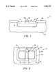
- FIG. 1 is a cross sectional view showing a portion of a typical integrated circuit element of the type which will benefit from the method and procedures of the present invention
- FIG. 2 is a plan view of the integrated circuit element shown in FIG. 1;
- FIG. 3 is a schematic plan view of a standard box in a box pattern useful for calibration purposes
- FIGS. 4 through 7 are schematic plan views showing preferred forms of test patterns used in accordance with the invention for measuring various forms of dimensional anomalies, specifically;
- FIG. 4 is a schematic plan view of a line and space test pattern used in accordance with the invention for measuring line shortening
- FIG. 5 is a schematic plan view of a line and space test pattern used in accordance with the invention for measuring right coma;
- FIG. 6 is a schematic plan view of a line and space test pattern used in accordance with the invention for measuring left coma;
- FIG. 7 is a schematic plan view of a pillar test pattern used in accordance with the invention for measuring focus
- FIG. 8 is a schematic plan view showing a configuration of nine pattern boxes which may be positioned in the margin of a die as well as the margin of the projected image;
- FIG. 9 is a schematic plan view of a complete die projection which may utilize multiple repetitions of the group of pattern boxes shown in FIG. 8 and which may be used to calibrate the optics of the system.
- a portion of a semiconductor wafer 11 which, for instance, may include an n-type substrate 13 having a p-type well 15 and n + implants 17 and 19.
- a bird beak 21 is formed in the field oxide 20.
- a gate 23 is formed with a gate oxide 25 and polysilicon 26 bridging the gap between the implants 17 and 19.
- the polysilicon of the gate should contact the field oxide 20, but just barely contact it.
- this overlap of the gate on the field oxide 20 should be in the neighborhood of 0.1 ⁇ m ⁇ 0.03 ⁇ m.
- the extension of the gate over the active regions represented by the implants 17 and 19 in FIGS. 1 and 2 should also be in the neighborhood of 0.1 ⁇ m ⁇ 0.06 ⁇ m.
- the pattern 27 includes the usual large square 28 with a small square 29 centrally disposed within the large square.
- the large square is ordinarily 20 ⁇ m on each side while the inner square is 10 ⁇ m on each side creating 5 ⁇ m spaces d 1 , d 2 , d 3 and d 4 between them. Since the large and small squares of the calibration pattern 27 are formed of solid lines, wide edges are provided against which the measurements of d 1 , d 2 , d 3 and d 4 can be made.
- the pattern of FIG. 3 provides a stable reference to focus values.
- test pattern 30 which can be used to determine line shortening.
- the measurement itself will reflect both focus and line shortening but, when it is compared with measurements from the test pattern 27 of FIG. 3, the degree of line shortening alone can be determined.
- the test pattern 27 includes an outer box 31 and an inner box 33.
- the outer box 31 may be 20 ⁇ m, with the inner box being 10 ⁇ m square.
- the distance d 5 between the left vertical side of the outer box and the left vertical side of the inner box is 5 ⁇ m.
- On the right side of the pattern there is no solid vertical line forming wide measurement edges from which the distance d 6 can be measured.
- the lines 35 each have a nominal length of 5 ⁇ m.
- the width of the lines 35 is selected to be the same as that of the lines of the semiconductor feature to be measured. For instance, referring to FIG. 2, if the gate 23 were to have a width D 2 of 0.35 ⁇ m, the width of the lines 35 in FIG. 4 would likewise be 0.35 ⁇ m.
- the lines are spaced from each other by a distance equal to the width of the lines.
- the test pattern 30 incorporates the dimensions as set forth above. However, when the pattern is projected onto the wafer and is photolithographed onto the wafer, the lines 35 will be shortened at both ends making the overall dimension d 6 of the imprinted pattern somewhat less than 5 ⁇ m. If there is any defocusing, the lines will be shortened even more.
- the degree of defocusing can be determined, the difference between the two being a measure of line shortening without regard to focus.
- Such measurements may easily be made using an overlay metrology tool such as Models 5100 or 5105 produced by KLA Instruments Corporation of Santa Clara, Calif. In making such measurements, the metrology tool recognizes the ends of the narrow horizontal lines just as it would a solid vertical side if the lines are spaced closely enough. However, its measurement will discern the line shortening and give an accurate measurement of the shortened lines.
- the measurements d 5 and d 6 will provide information leading to the measurement of line shortening and focus along the horizontal axis, but a comparison of the measurements d 7 and d 8 will provide the same quantitative analysis as to vertical axis.
- the test pattern 36 is the same size as the pattern 30 shown in FIG. 4 and differs from the pattern 30 only in that, instead of the lines 35, the test pattern of FIG. 5 includes shorter finger like elements 37 which extend from the right edge of the large square 39, but do not extend all the way to the small square 41. Preferably, the fingers 37 extend across half the distance between the inner and outer squares.
- the test pattern 36 includes a solid portion 43 extending from the inside end of the fingers 37 to the right side of the small square 41. Again, the width of the fingers 37 is comparable to the width of the lines 35 in the test pattern 30, dependent upon the size of the lines actually to be formed on the wafer.
- measurement d 9 will again be 5 ⁇ m.
- the measurement d 10 will be 5 ⁇ m as measured at the mask, but, depending upon the degree of defocus, line shortening and right coma aberration, the actual measurement of d 10 as projected onto the wafer is somewhat shorter.
- the test pattern 44 shown in FIG. 6 is identical to the pattern 36 except that the pattern 44 measures left coma as opposed to right coma. Measurements of left coma are made in the same fashion as those for right coma. After taking the measurement d 10 for right coma and the corresponding measurement for left coma, the reduced length of lines due to coma can be determined simply by comparing the two measurements. If the measurements from the test patterns 36 are equal, there is no coma. If the measurement of the test pattern 36 is shorter, there is right coma. Conversely, if the measurement of the test pattern 44 is shorter, there is left coma. The degree of coma is determined by the difference in the measurements of the two test patterns.
- the pattern 45 instead of the lines of the pattern 30 or the shorter fingers of the patterns 36 and 44, the pattern includes a series of squares 46 each having a length and width determined by the width of the lines being produced on the wafer.
- the squares 46 may be separated from each other by distances less than their individual lengths.
- the gate lines 23 of FIGS. 1 and 2 have a width of 0.35 ⁇ m
- the sides of each of the squares 46 should likewise be 0.35 ⁇ m.
- These small squares appear as microscopic towers or "pillars" since they are formed of resist material usually having a thickness three or more times greater than the side dimensions in the neighborhood of 0.2 ⁇ m to 0.4 ⁇ m.
- the measurements d 11 and d 12 are both 5 ⁇ m when considered at the mask, but when the measurement d 12 is projected onto the wafer it will be somewhat less due to the action of light around all sides of the small pillar, and thus the degree of defocusing can be even more critically determined.
- the large and the small boxes be imprinted separately. Rather, they can be both imprinted simultaneously since the measurement is related to the lens rather than the action of a stepper or the like. Thus a single exposure of a single mask will be sufficient.
- the mask can be provided not only for one of the patterns such as shown in FIGS. 3 thru 7, but a clump of such patterns may be provided as shown in FIG. 8. Referring specifically to FIG. 8, there is shown a mask 60 in accordance with the invention with nine different patterns.
- Patterns 61, 62, 63 and 64 may be made for use with lines having one width, such for instance, as 0.30 ⁇ m, whereas patterns 66 thru 69 may be used with a thicker line such as 0.35 ⁇ m.
- the patterns 61 and 66 are similar to the pattern of FIG. 4 and suitable for the measurement of focus; patterns 62 and 67 are for measuring right coma; patterns 63 and 68 are for measuring left coma; and patterns 64 and 69 are pillar patterns for more critical measure of focus.
- the central pattern 65 is a standard box in a box used for calibration purposes.
- the entire clump of patterns as shown in FIG. 8 can be imprinted at several locations in the margins of the die and in those instances where multiple dies are printed in a single shot, at several locations in the boarders between those dies.
- Each clump of patterns at the several locations will include test patterns 30 as shown in FIG. 4 and, at each of these sites, multiple measurements of the distances d 5 and d 6 are made at different degrees of defocus and at nominal focus. These measurements can be used to determine the amount of line shortening and the amount of correction required.
- curves can then be plotted to reflect the degree of misregistration for each focus setting. With the information as to the degree of misregistration at various sites on the mask, corrective measures may be taken such as tilting the table carrying the wafer or by adjusting the circuit mask itself with Optical Proximity Correction (OPC).
- OPC Optical Proximity Correction
- test patterns 27, 36, 44 and 45 of FIGS. 3, 5, 6 and 7 are also replicated at each of the various sites, and the corresponding measurements of those patterns are made at different degrees of defocus and at nominal focus. These measurements can be used to determine the amount of left and right coma as well as a more critical defocus determination. Again, the measurements may be used to determine the amount of correction required. For each site, curves can then be plotted to reflect the degree of misregistration for each focus setting.
- FIG. 9 wherein the entire mask 71 measuring 20 mm ⁇ 25 mm includes numerous patterns 60 as the type shown in FIG. 8. With such an arrangement, the operation of the lens throughout its entire projection area can be measured for all of the aforementioned aberrations.
Abstract
Description
Claims (22)
Priority Applications (3)
| Application Number | Priority Date | Filing Date | Title |
|---|---|---|---|
| US08/826,482 US5902703A (en) | 1997-03-27 | 1997-03-27 | Method for measuring dimensional anomalies in photolithographed integrated circuits using overlay metrology, and masks therefor |
| US08/951,396 US5962173A (en) | 1997-03-27 | 1997-10-16 | Method for measuring the effectiveness of optical proximity corrections |
| US09/264,742 US6301008B1 (en) | 1997-03-27 | 1999-03-08 | Arrangement and method for calibrating optical line shortening measurements |
Applications Claiming Priority (1)
| Application Number | Priority Date | Filing Date | Title |
|---|---|---|---|
| US08/826,482 US5902703A (en) | 1997-03-27 | 1997-03-27 | Method for measuring dimensional anomalies in photolithographed integrated circuits using overlay metrology, and masks therefor |
Related Child Applications (1)
| Application Number | Title | Priority Date | Filing Date |
|---|---|---|---|
| US08/951,396 Continuation-In-Part US5962173A (en) | 1997-03-27 | 1997-10-16 | Method for measuring the effectiveness of optical proximity corrections |
Publications (1)
| Publication Number | Publication Date |
|---|---|
| US5902703A true US5902703A (en) | 1999-05-11 |
Family
ID=25246653
Family Applications (1)
| Application Number | Title | Priority Date | Filing Date |
|---|---|---|---|
| US08/826,482 Expired - Fee Related US5902703A (en) | 1997-03-27 | 1997-03-27 | Method for measuring dimensional anomalies in photolithographed integrated circuits using overlay metrology, and masks therefor |
Country Status (1)
| Country | Link |
|---|---|
| US (1) | US5902703A (en) |
Cited By (36)
| Publication number | Priority date | Publication date | Assignee | Title |
|---|---|---|---|---|
| US6127075A (en) * | 1998-09-08 | 2000-10-03 | Mosel Vitelic Incorporated | Method for checking accuracy of a measuring instrument for overlay registration |
| EP1081483A3 (en) * | 1999-09-03 | 2001-08-16 | Oki Electric Industry Company, Limited | Stepper lens aberration measurement pattern and stepper lens aberration characteristics evaluating method |
| EP1162507A2 (en) * | 2000-06-08 | 2001-12-12 | Kabushiki Kaisha Toshiba | Alignment method, overlay deviation inspection method and photomask |
| US6462818B1 (en) | 2000-06-22 | 2002-10-08 | Kla-Tencor Corporation | Overlay alignment mark design |
| US6486954B1 (en) | 2000-09-01 | 2002-11-26 | Kla-Tencor Technologies Corporation | Overlay alignment measurement mark |
| US20030002043A1 (en) * | 2001-04-10 | 2003-01-02 | Kla-Tencor Corporation | Periodic patterns and technique to control misalignment |
| US20030044696A1 (en) * | 2001-08-29 | 2003-03-06 | Taiwan Semiconductor Manufacturing Co. Ltd. | Verification photomask |
| US20030048458A1 (en) * | 2001-06-26 | 2003-03-13 | Walter Mieher | Method for determining lithographic focus and exposure |
| US6602728B1 (en) * | 2001-01-05 | 2003-08-05 | International Business Machines Corporation | Method for generating a proximity model based on proximity rules |
| US20030223630A1 (en) * | 2002-02-15 | 2003-12-04 | Kla-Tencor Corporation | Overlay metrology and control method |
| US20030232253A1 (en) * | 2002-06-18 | 2003-12-18 | Pierre Leroux | Techniques to characterize iso-dense effects for microdevice manufacture |
| US6671396B1 (en) | 2000-09-18 | 2003-12-30 | Taiwan Semiconductor Manufacturing Company | Method to monitor stepper lens quality in color filter process |
| US6750961B2 (en) * | 2001-01-26 | 2004-06-15 | Timbre Technologies, Inc. | System and method for characterizing macro-grating test patterns in advanced lithography and etch processes |
| US6757629B2 (en) * | 2000-12-22 | 2004-06-29 | Fujitsu Limited | Calibration plate having accurately defined calibration pattern |
| US6766507B2 (en) | 2002-04-12 | 2004-07-20 | International Business Machines Corporation | Mask/wafer control structure and algorithm for placement |
| US20040190008A1 (en) * | 2003-01-17 | 2004-09-30 | Kla-Tencor Corporation | Method for process optimization and control by comparison between 2 or more measured scatterometry signals |
| US20040212796A1 (en) * | 2003-04-25 | 2004-10-28 | Michael Adel | Method and mark for metrology of phase errors on phase shift masks |
| WO2004097528A2 (en) | 2003-04-29 | 2004-11-11 | Koninklijke Philips Electronics N.V. | System and method for characterizing lithography effects on a wafer |
| WO2005013004A2 (en) * | 2003-08-01 | 2005-02-10 | Koninklijke Philips Electronics N.V. | Measuring the effect of flare on line width |
| US6921916B2 (en) | 2000-08-30 | 2005-07-26 | Kla -Tenocor Technologies Corporation | Overlay marks, methods of overlay mark design and methods of overlay measurements |
| US20050209636A1 (en) * | 2004-01-30 | 2005-09-22 | Nmt Medical, Inc. | Devices, systems, and methods for closure of cardiac openings |
| US20050250026A1 (en) * | 2004-05-07 | 2005-11-10 | Koninklijke Philips Electronics N.V. | Overlay box structure for measuring process induced line shortening effect |
| US20060078804A1 (en) * | 2004-10-13 | 2006-04-13 | David Ziger | Calibration of optical line shortening measurements |
| US20060080046A1 (en) * | 2004-10-13 | 2006-04-13 | David Ziger | Measuring flare in semiconductor lithography |
| US7346878B1 (en) | 2003-07-02 | 2008-03-18 | Kla-Tencor Technologies Corporation | Apparatus and methods for providing in-chip microtargets for metrology or inspection |
| US7557921B1 (en) | 2005-01-14 | 2009-07-07 | Kla-Tencor Technologies Corporation | Apparatus and methods for optically monitoring the fidelity of patterns produced by photolitographic tools |
| US7608468B1 (en) | 2003-07-02 | 2009-10-27 | Kla-Tencor Technologies, Corp. | Apparatus and methods for determining overlay and uses of same |
| CN1902501B (en) * | 2003-07-17 | 2010-06-09 | 凸版光掩膜公司 | Method and apparatus for calibrating a metrology tool |
| CN1641485B (en) * | 2004-01-16 | 2011-05-25 | 株式会社东芝 | Exposure system method for evaluating lithography process |
| US20120064666A1 (en) * | 2009-02-20 | 2012-03-15 | Sumitomo Metal Mining Co., Ltd. | Manufacturing method of substrate for a semiconductor package, manufacturing method of semiconductor package, substrate for a semiconductor package and semiconductor package |
| US8138498B2 (en) | 2000-08-30 | 2012-03-20 | Kla-Tencor Technologies Corporation | Apparatus and methods for determining overlay of structures having rotational or mirror symmetry |
| US8443309B2 (en) | 2011-03-04 | 2013-05-14 | International Business Machines Corporation | Multifeature test pattern for optical proximity correction model verification |
| US9927718B2 (en) | 2010-08-03 | 2018-03-27 | Kla-Tencor Corporation | Multi-layer overlay metrology target and complimentary overlay metrology measurement systems |
| US10451412B2 (en) | 2016-04-22 | 2019-10-22 | Kla-Tencor Corporation | Apparatus and methods for detecting overlay errors using scatterometry |
| US20200105764A1 (en) * | 2018-09-27 | 2020-04-02 | United Microelectronics Corp. | Method of forming layout definition of semiconductor device |
| US10890436B2 (en) | 2011-07-19 | 2021-01-12 | Kla Corporation | Overlay targets with orthogonal underlayer dummyfill |
Citations (7)
| Publication number | Priority date | Publication date | Assignee | Title |
|---|---|---|---|---|
| US5328807A (en) * | 1990-06-11 | 1994-07-12 | Hitichi, Ltd. | Method of forming a pattern |
| US5439765A (en) * | 1992-04-02 | 1995-08-08 | Nec Corporation | Photomask for semiconductor integrated circuit device |
| US5447810A (en) * | 1994-02-09 | 1995-09-05 | Microunity Systems Engineering, Inc. | Masks for improved lithographic patterning for off-axis illumination lithography |
| US5700602A (en) * | 1992-08-21 | 1997-12-23 | Intel Corporation | Method and apparatus for precision determination of phase-shift in a phase-shifted reticle |
| US5731109A (en) * | 1995-06-15 | 1998-03-24 | Hyundai Electronics Industries Co., Ltd. | Pattern structure of photomask comprising a sawtooth pattern |
| US5798195A (en) * | 1993-09-24 | 1998-08-25 | Nikon Corporation | Stepping accuracy measuring method |
| US5800951A (en) * | 1995-11-22 | 1998-09-01 | Nec Corporation | Exposure method and exposure mask with monitoring patterns |
-
1997
- 1997-03-27 US US08/826,482 patent/US5902703A/en not_active Expired - Fee Related
Patent Citations (7)
| Publication number | Priority date | Publication date | Assignee | Title |
|---|---|---|---|---|
| US5328807A (en) * | 1990-06-11 | 1994-07-12 | Hitichi, Ltd. | Method of forming a pattern |
| US5439765A (en) * | 1992-04-02 | 1995-08-08 | Nec Corporation | Photomask for semiconductor integrated circuit device |
| US5700602A (en) * | 1992-08-21 | 1997-12-23 | Intel Corporation | Method and apparatus for precision determination of phase-shift in a phase-shifted reticle |
| US5798195A (en) * | 1993-09-24 | 1998-08-25 | Nikon Corporation | Stepping accuracy measuring method |
| US5447810A (en) * | 1994-02-09 | 1995-09-05 | Microunity Systems Engineering, Inc. | Masks for improved lithographic patterning for off-axis illumination lithography |
| US5731109A (en) * | 1995-06-15 | 1998-03-24 | Hyundai Electronics Industries Co., Ltd. | Pattern structure of photomask comprising a sawtooth pattern |
| US5800951A (en) * | 1995-11-22 | 1998-09-01 | Nec Corporation | Exposure method and exposure mask with monitoring patterns |
Cited By (99)
| Publication number | Priority date | Publication date | Assignee | Title |
|---|---|---|---|---|
| US6127075A (en) * | 1998-09-08 | 2000-10-03 | Mosel Vitelic Incorporated | Method for checking accuracy of a measuring instrument for overlay registration |
| US6654107B1 (en) | 1999-09-03 | 2003-11-25 | Oki Electric Industry Co., Ltd. | Stepper lens aberration measurement pattern and stepper lens aberration characteristics evaluating method |
| EP1081483A3 (en) * | 1999-09-03 | 2001-08-16 | Oki Electric Industry Company, Limited | Stepper lens aberration measurement pattern and stepper lens aberration characteristics evaluating method |
| EP1162507A2 (en) * | 2000-06-08 | 2001-12-12 | Kabushiki Kaisha Toshiba | Alignment method, overlay deviation inspection method and photomask |
| EP1162507A3 (en) * | 2000-06-08 | 2005-01-05 | Kabushiki Kaisha Toshiba | Alignment method, overlay deviation inspection method and photomask |
| US6462818B1 (en) | 2000-06-22 | 2002-10-08 | Kla-Tencor Corporation | Overlay alignment mark design |
| US7102749B2 (en) | 2000-06-22 | 2006-09-05 | Kla-Tencor | Overlay alignment mark design |
| US20050174574A1 (en) * | 2000-06-22 | 2005-08-11 | Kla-Tencor Corporation | Overlay alignment mark design |
| US6894783B2 (en) | 2000-06-22 | 2005-05-17 | Kla-Tencor Corporation | Overlay alignment mark design |
| US6580505B1 (en) | 2000-06-22 | 2003-06-17 | Kla-Tencor Corporation | Overlay alignment mark design |
| US7181057B2 (en) | 2000-08-30 | 2007-02-20 | Kla-Tencor Technologies Corporation | Overlay marks, methods of overlay mark design and methods of overlay measurements |
| US6985618B2 (en) | 2000-08-30 | 2006-01-10 | Kla-Tencor Technologies Corporation | Overlay marks, methods of overlay mark design and methods of overlay measurements |
| US9702693B2 (en) | 2000-08-30 | 2017-07-11 | Kla-Tencor Corporation | Apparatus for measuring overlay errors |
| US9347879B2 (en) | 2000-08-30 | 2016-05-24 | Kla-Tencor Corporation | Apparatus and methods for detecting overlay errors using scatterometry |
| US9182680B2 (en) | 2000-08-30 | 2015-11-10 | Kla-Tencor Corporation | Apparatus and methods for determining overlay of structures having rotational or mirror symmetry |
| USRE45245E1 (en) | 2000-08-30 | 2014-11-18 | Kla-Tencor Corporation | Apparatus and methods for determining overlay of structures having rotational or mirror symmetry |
| US8330281B2 (en) | 2000-08-30 | 2012-12-11 | Kla-Tencor Technologies Corporation | Overlay marks, methods of overlay mark design and methods of overlay measurements |
| US8138498B2 (en) | 2000-08-30 | 2012-03-20 | Kla-Tencor Technologies Corporation | Apparatus and methods for determining overlay of structures having rotational or mirror symmetry |
| US7879627B2 (en) | 2000-08-30 | 2011-02-01 | Kla-Tencor Technologies Corporation | Overlay marks and methods of manufacturing such marks |
| US20090291513A1 (en) * | 2000-08-30 | 2009-11-26 | Kla-Tencor Corporation | Overlay marks, methods of overlay mark design and methods of overlay measurements |
| US7274814B2 (en) | 2000-08-30 | 2007-09-25 | Kla-Tencor Corporation | Overlay marks, methods of overlay mark design and methods of overlay measurements |
| US20080023855A1 (en) * | 2000-08-30 | 2008-01-31 | Kla-Tencor Corporation | Overlay marks, methods of overlay mark design and methods of overlay measurements |
| US7317824B2 (en) | 2000-08-30 | 2008-01-08 | Kla-Tencor Technologies Corporation | Overlay marks, methods of overlay mark design and methods of overlay measurements |
| US7355291B2 (en) | 2000-08-30 | 2008-04-08 | Kla-Tencor Technologies Corporation | Overlay marks, methods of overlay mark design and methods of overlay measurements |
| US7177457B2 (en) | 2000-08-30 | 2007-02-13 | Kla-Tencor Corporation | Overlay marks, methods of overlay mark design and methods of overlay measurements |
| US20060204073A1 (en) * | 2000-08-30 | 2006-09-14 | Kla-Tencor Corporation | Overlay marks, methods of overlay mark design and methods of overlay measurements |
| US20060177120A1 (en) * | 2000-08-30 | 2006-08-10 | Kla-Tencor Corporation | Overlay marks, methods of overlay mark design and methods of overlay measurements |
| US6921916B2 (en) | 2000-08-30 | 2005-07-26 | Kla -Tenocor Technologies Corporation | Overlay marks, methods of overlay mark design and methods of overlay measurements |
| US7068833B1 (en) | 2000-08-30 | 2006-06-27 | Kla-Tencor Corporation | Overlay marks, methods of overlay mark design and methods of overlay measurements |
| US20060039595A1 (en) * | 2000-08-30 | 2006-02-23 | Kla-Tencor Technologies Corporation | Overlay marks, methods of overlay mark design and methods of overlay measurements |
| US6486954B1 (en) | 2000-09-01 | 2002-11-26 | Kla-Tencor Technologies Corporation | Overlay alignment measurement mark |
| US6671396B1 (en) | 2000-09-18 | 2003-12-30 | Taiwan Semiconductor Manufacturing Company | Method to monitor stepper lens quality in color filter process |
| US6757629B2 (en) * | 2000-12-22 | 2004-06-29 | Fujitsu Limited | Calibration plate having accurately defined calibration pattern |
| US6602728B1 (en) * | 2001-01-05 | 2003-08-05 | International Business Machines Corporation | Method for generating a proximity model based on proximity rules |
| US6750961B2 (en) * | 2001-01-26 | 2004-06-15 | Timbre Technologies, Inc. | System and method for characterizing macro-grating test patterns in advanced lithography and etch processes |
| US9103662B2 (en) | 2001-04-10 | 2015-08-11 | Kla-Tencor Corporation | Periodic patterns and technique to control misalignment between two layers |
| US8570515B2 (en) | 2001-04-10 | 2013-10-29 | Kla-Tencor Corporation | Periodic patterns and technique to control misalignment between two layers |
| US9476698B2 (en) | 2001-04-10 | 2016-10-25 | Kla-Tencor Corporation | Periodic patterns and technique to control misalignment between two layers |
| US20060132807A1 (en) * | 2001-04-10 | 2006-06-22 | Ibrahim Abdulhalim | Periodic patterns and technique to control misalignment between two layers |
| US20040229471A1 (en) * | 2001-04-10 | 2004-11-18 | Ibrahim Abdulhalim | Periodic patterns and technique to control misalignment between two layers |
| US9835447B2 (en) | 2001-04-10 | 2017-12-05 | Kla-Tencor Corporation | Periodic patterns and technique to control misalignment between two layers |
| US9234745B2 (en) | 2001-04-10 | 2016-01-12 | Kla-Tencor Corporation | Periodic patterns and techniques to control misalignment between two layers |
| US7656528B2 (en) | 2001-04-10 | 2010-02-02 | Kla-Tencor Corporation | Periodic patterns and technique to control misalignment between two layers |
| US20030002043A1 (en) * | 2001-04-10 | 2003-01-02 | Kla-Tencor Corporation | Periodic patterns and technique to control misalignment |
| US8525994B2 (en) | 2001-04-10 | 2013-09-03 | Kla-Tencor Corporation | Periodic patterns and technique to control misaligment between two layers |
| US20090231584A1 (en) * | 2001-04-10 | 2009-09-17 | Kla-Tencor Technology Corporation | Periodic patterns and technique to control misaligment between two layers |
| US20060262326A1 (en) * | 2001-04-10 | 2006-11-23 | Ibrahim Abdulhalim | Periodic patterns and technique to control misalignment between two layers |
| US10151584B2 (en) | 2001-04-10 | 2018-12-11 | Kla-Tencor Corporation | Periodic patterns and technique to control misalignment between two layers |
| US20060065625A1 (en) * | 2001-04-10 | 2006-03-30 | Ibrahim Abdulhalim | Periodic patterns and technique to control misalignment between two layers |
| US20050208685A1 (en) * | 2001-04-10 | 2005-09-22 | Ibrahim Abdulhalim | Periodic patterns and technique to control misalignment |
| US20030048458A1 (en) * | 2001-06-26 | 2003-03-13 | Walter Mieher | Method for determining lithographic focus and exposure |
| US7382447B2 (en) | 2001-06-26 | 2008-06-03 | Kla-Tencor Technologies Corporation | Method for determining lithographic focus and exposure |
| US6824931B2 (en) * | 2001-08-29 | 2004-11-30 | Taiwan Semiconductor Manufacturing Co., Ltd | Verification photomask |
| US20030044696A1 (en) * | 2001-08-29 | 2003-03-06 | Taiwan Semiconductor Manufacturing Co. Ltd. | Verification photomask |
| US20030223630A1 (en) * | 2002-02-15 | 2003-12-04 | Kla-Tencor Corporation | Overlay metrology and control method |
| US7804994B2 (en) | 2002-02-15 | 2010-09-28 | Kla-Tencor Technologies Corporation | Overlay metrology and control method |
| US6766507B2 (en) | 2002-04-12 | 2004-07-20 | International Business Machines Corporation | Mask/wafer control structure and algorithm for placement |
| US20030232253A1 (en) * | 2002-06-18 | 2003-12-18 | Pierre Leroux | Techniques to characterize iso-dense effects for microdevice manufacture |
| US6800403B2 (en) | 2002-06-18 | 2004-10-05 | Koninklijke Philips Electronics N.V. | Techniques to characterize iso-dense effects for microdevice manufacture |
| US20040190008A1 (en) * | 2003-01-17 | 2004-09-30 | Kla-Tencor Corporation | Method for process optimization and control by comparison between 2 or more measured scatterometry signals |
| US7352453B2 (en) | 2003-01-17 | 2008-04-01 | Kla-Tencor Technologies Corporation | Method for process optimization and control by comparison between 2 or more measured scatterometry signals |
| US20040212796A1 (en) * | 2003-04-25 | 2004-10-28 | Michael Adel | Method and mark for metrology of phase errors on phase shift masks |
| US7075639B2 (en) | 2003-04-25 | 2006-07-11 | Kla-Tencor Technologies Corporation | Method and mark for metrology of phase errors on phase shift masks |
| US7368208B1 (en) | 2003-04-25 | 2008-05-06 | Kla-Tencor Technologies Corp. | Measuring phase errors on phase shift masks |
| WO2004097528A2 (en) | 2003-04-29 | 2004-11-11 | Koninklijke Philips Electronics N.V. | System and method for characterizing lithography effects on a wafer |
| US20070275329A1 (en) * | 2003-04-29 | 2007-11-29 | Koninklijke Philips Electronics N.V. | System and Method for Characterizing Lithography Effects on a Wafer |
| US7537939B2 (en) | 2003-04-29 | 2009-05-26 | Nxp B.V. | System and method for characterizing lithography effects on a wafer |
| US7876438B2 (en) | 2003-07-02 | 2011-01-25 | Kla-Tencor Technologies Corporation | Apparatus and methods for determining overlay and uses of same |
| US7346878B1 (en) | 2003-07-02 | 2008-03-18 | Kla-Tencor Technologies Corporation | Apparatus and methods for providing in-chip microtargets for metrology or inspection |
| US7608468B1 (en) | 2003-07-02 | 2009-10-27 | Kla-Tencor Technologies, Corp. | Apparatus and methods for determining overlay and uses of same |
| US20100005442A1 (en) * | 2003-07-02 | 2010-01-07 | Kla-Tencor Technologies Corporation | Apparatus and Methods for Determining Overlay and Uses of Same |
| CN1902501B (en) * | 2003-07-17 | 2010-06-09 | 凸版光掩膜公司 | Method and apparatus for calibrating a metrology tool |
| US20060210885A1 (en) * | 2003-08-01 | 2006-09-21 | David Ziger | Measuring the effect of flare on line width |
| WO2005013004A3 (en) * | 2003-08-01 | 2005-07-21 | Koninkl Philips Electronics Nv | Measuring the effect of flare on line width |
| CN1833205B (en) * | 2003-08-01 | 2011-02-16 | Nxp股份有限公司 | Measuring the effect of flare on line width |
| WO2005013004A2 (en) * | 2003-08-01 | 2005-02-10 | Koninklijke Philips Electronics N.V. | Measuring the effect of flare on line width |
| US7556900B2 (en) | 2003-08-01 | 2009-07-07 | Nxp B.V. | Measuring the effect of flare on line width |
| CN1641485B (en) * | 2004-01-16 | 2011-05-25 | 株式会社东芝 | Exposure system method for evaluating lithography process |
| US20050209636A1 (en) * | 2004-01-30 | 2005-09-22 | Nmt Medical, Inc. | Devices, systems, and methods for closure of cardiac openings |
| US20050250026A1 (en) * | 2004-05-07 | 2005-11-10 | Koninklijke Philips Electronics N.V. | Overlay box structure for measuring process induced line shortening effect |
| US7332255B2 (en) * | 2004-05-07 | 2008-02-19 | Nxp B.V. | Overlay box structure for measuring process induced line shortening effect |
| WO2006040347A1 (en) * | 2004-10-13 | 2006-04-20 | Infineon Technologies Ag | Calibration of optical line shortening measurements |
| US20060080046A1 (en) * | 2004-10-13 | 2006-04-13 | David Ziger | Measuring flare in semiconductor lithography |
| US8717539B2 (en) | 2004-10-13 | 2014-05-06 | Infineon Technologies Ag | Calibration of optical line shortening measurements |
| US20090198468A1 (en) * | 2004-10-13 | 2009-08-06 | David Ziger | Calibration of Optical Line Shortening Measurements |
| US20110035171A1 (en) * | 2004-10-13 | 2011-02-10 | David Ziger | Calibration of Optical Line Shortening Measurements |
| US7096127B2 (en) | 2004-10-13 | 2006-08-22 | Infineon Technologies Ag | Measuring flare in semiconductor lithography |
| US7842439B2 (en) | 2004-10-13 | 2010-11-30 | Infineon Technologies Ag | Calibration of optical line shortening measurements |
| US7541121B2 (en) * | 2004-10-13 | 2009-06-02 | Infineon Technologies Ag | Calibration of optical line shortening measurements |
| US20060078804A1 (en) * | 2004-10-13 | 2006-04-13 | David Ziger | Calibration of optical line shortening measurements |
| US7557921B1 (en) | 2005-01-14 | 2009-07-07 | Kla-Tencor Technologies Corporation | Apparatus and methods for optically monitoring the fidelity of patterns produced by photolitographic tools |
| US20120064666A1 (en) * | 2009-02-20 | 2012-03-15 | Sumitomo Metal Mining Co., Ltd. | Manufacturing method of substrate for a semiconductor package, manufacturing method of semiconductor package, substrate for a semiconductor package and semiconductor package |
| US9927718B2 (en) | 2010-08-03 | 2018-03-27 | Kla-Tencor Corporation | Multi-layer overlay metrology target and complimentary overlay metrology measurement systems |
| US10527954B2 (en) | 2010-08-03 | 2020-01-07 | Kla-Tencor Corporation | Multi-layer overlay metrology target and complimentary overlay metrology measurement systems |
| US8443309B2 (en) | 2011-03-04 | 2013-05-14 | International Business Machines Corporation | Multifeature test pattern for optical proximity correction model verification |
| US10890436B2 (en) | 2011-07-19 | 2021-01-12 | Kla Corporation | Overlay targets with orthogonal underlayer dummyfill |
| US10451412B2 (en) | 2016-04-22 | 2019-10-22 | Kla-Tencor Corporation | Apparatus and methods for detecting overlay errors using scatterometry |
| US20200105764A1 (en) * | 2018-09-27 | 2020-04-02 | United Microelectronics Corp. | Method of forming layout definition of semiconductor device |
| US10795255B2 (en) * | 2018-09-27 | 2020-10-06 | United Microelectronics Corp. | Method of forming layout definition of semiconductor device |
Similar Documents
| Publication | Publication Date | Title |
|---|---|---|
| US5902703A (en) | Method for measuring dimensional anomalies in photolithographed integrated circuits using overlay metrology, and masks therefor | |
| US6778275B2 (en) | Aberration mark and method for estimating overlay error and optical aberrations | |
| KR100189287B1 (en) | Registration accuracy measurement mark | |
| US7655369B2 (en) | Reticle set, method for designing a reticle set, exposure monitoring method, inspection method for reticle set and manufacturing method for a semiconductor device | |
| US6083807A (en) | Overlay measuring mark and its method | |
| JPH06132189A (en) | Method for optimizing measurement conditions of overlapping accuracy measuring device and method for optimizing alignment mark shape or alignment mark measurement system in exposure device | |
| US7078691B2 (en) | Standard reference for metrology and calibration method of electron-beam metrology system using the same | |
| JP3371852B2 (en) | Reticle | |
| JPH1069066A (en) | Mask and its inspection method and exposure method | |
| US7842439B2 (en) | Calibration of optical line shortening measurements | |
| US7008731B2 (en) | Method of manufacturing a photomask and method of manufacturing a semiconductor device using the photomask | |
| GB2287328A (en) | Method for fabricating a photomask | |
| JP2682523B2 (en) | Exposure method and monitor pattern | |
| JPH09166866A (en) | Mark for aligning photomask and semiconductor device | |
| US6536130B1 (en) | Overlay mark for concurrently monitoring alignment accuracy, focus, leveling and astigmatism and method of application thereof | |
| JPH11102061A (en) | Photomask pattern for projection exposure, photomask for projection exposure, focusing position detecting method, focusing position control method, and manufacture of semiconductor device | |
| JP3511552B2 (en) | Superposition measurement mark and measurement method | |
| KR20000047483A (en) | Exposure method and device manufacturing method using the same | |
| US6943458B2 (en) | Semiconductor device and manufacturing method thereof, and registration accuracy measurement enhancement method | |
| US20020031712A1 (en) | Photomask making method and alignment method | |
| US7136520B2 (en) | Method of checking alignment accuracy of patterns on stacked semiconductor layers | |
| CN1833205B (en) | Measuring the effect of flare on line width | |
| US8198105B2 (en) | Monitor for variation of critical dimensions (CDs) of reticles | |
| US5928820A (en) | Method for measuring pattern line width during manufacture of a semiconductor device | |
| US5552251A (en) | Reticle and method for measuring rotation error of reticle by use of the reticle |
Legal Events
| Date | Code | Title | Description |
|---|---|---|---|
| AS | Assignment |
Owner name: VLSI TECHNOLOGY, INC., CALIFORNIA Free format text: ASSIGNMENT OF ASSIGNORS INTEREST;ASSIGNORS:LEROUX, PIERRE;SATYENDRA, SETHI;ZIGER, DAVID;REEL/FRAME:008695/0523;SIGNING DATES FROM 19970326 TO 19970327 Owner name: VLSI TECHNOLOGY, INC., CALIFORNIA Free format text: ASSIGNMENT OF ASSIGNORS INTEREST;ASSIGNORS:LEROUX, PIERRE;SATYENDRA, SETHI;ZIGER, DAVID;REEL/FRAME:008496/0550;SIGNING DATES FROM 19970326 TO 19970327 |
|
| FEPP | Fee payment procedure |
Free format text: PAYOR NUMBER ASSIGNED (ORIGINAL EVENT CODE: ASPN); ENTITY STATUS OF PATENT OWNER: LARGE ENTITY |
|
| FPAY | Fee payment |
Year of fee payment: 4 |
|
| REMI | Maintenance fee reminder mailed | ||
| LAPS | Lapse for failure to pay maintenance fees | ||
| STCH | Information on status: patent discontinuation |
Free format text: PATENT EXPIRED DUE TO NONPAYMENT OF MAINTENANCE FEES UNDER 37 CFR 1.362 |