US5898548A - Shielded magnetic tunnel junction magnetoresistive read head - Google Patents
Shielded magnetic tunnel junction magnetoresistive read head Download PDFInfo
- Publication number
- US5898548A US5898548A US08/957,787 US95778797A US5898548A US 5898548 A US5898548 A US 5898548A US 95778797 A US95778797 A US 95778797A US 5898548 A US5898548 A US 5898548A
- Authority
- US
- United States
- Prior art keywords
- layer
- head
- shield
- spacer
- magnetic
- Prior art date
- Legal status (The legal status is an assumption and is not a legal conclusion. Google has not performed a legal analysis and makes no representation as to the accuracy of the status listed.)
- Expired - Lifetime
Links
Images


Classifications
-
- G—PHYSICS
- G11—INFORMATION STORAGE
- G11B—INFORMATION STORAGE BASED ON RELATIVE MOVEMENT BETWEEN RECORD CARRIER AND TRANSDUCER
- G11B5/00—Recording by magnetisation or demagnetisation of a record carrier; Reproducing by magnetic means; Record carriers therefor
- G11B5/127—Structure or manufacture of heads, e.g. inductive
- G11B5/33—Structure or manufacture of flux-sensitive heads, i.e. for reproduction only; Combination of such heads with means for recording or erasing only
- G11B5/332—Structure or manufacture of flux-sensitive heads, i.e. for reproduction only; Combination of such heads with means for recording or erasing only using thin films
-
- G—PHYSICS
- G11—INFORMATION STORAGE
- G11B—INFORMATION STORAGE BASED ON RELATIVE MOVEMENT BETWEEN RECORD CARRIER AND TRANSDUCER
- G11B5/00—Recording by magnetisation or demagnetisation of a record carrier; Reproducing by magnetic means; Record carriers therefor
- G11B5/127—Structure or manufacture of heads, e.g. inductive
- G11B5/33—Structure or manufacture of flux-sensitive heads, i.e. for reproduction only; Combination of such heads with means for recording or erasing only
- G11B5/39—Structure or manufacture of flux-sensitive heads, i.e. for reproduction only; Combination of such heads with means for recording or erasing only using magneto-resistive devices or effects
- G11B5/3903—Structure or manufacture of flux-sensitive heads, i.e. for reproduction only; Combination of such heads with means for recording or erasing only using magneto-resistive devices or effects using magnetic thin film layers or their effects, the films being part of integrated structures
- G11B5/3906—Details related to the use of magnetic thin film layers or to their effects
- G11B5/3909—Arrangements using a magnetic tunnel junction
-
- G—PHYSICS
- G11—INFORMATION STORAGE
- G11B—INFORMATION STORAGE BASED ON RELATIVE MOVEMENT BETWEEN RECORD CARRIER AND TRANSDUCER
- G11B5/00—Recording by magnetisation or demagnetisation of a record carrier; Reproducing by magnetic means; Record carriers therefor
- G11B5/127—Structure or manufacture of heads, e.g. inductive
- G11B5/33—Structure or manufacture of flux-sensitive heads, i.e. for reproduction only; Combination of such heads with means for recording or erasing only
- G11B5/39—Structure or manufacture of flux-sensitive heads, i.e. for reproduction only; Combination of such heads with means for recording or erasing only using magneto-resistive devices or effects
- G11B5/3903—Structure or manufacture of flux-sensitive heads, i.e. for reproduction only; Combination of such heads with means for recording or erasing only using magneto-resistive devices or effects using magnetic thin film layers or their effects, the films being part of integrated structures
- G11B5/3906—Details related to the use of magnetic thin film layers or to their effects
- G11B5/3912—Arrangements in which the active read-out elements are transducing in association with active magnetic shields, e.g. magnetically coupled shields
Definitions
- This invention relates in general to magnetic tunnel junction (MTJ) devices, and more particularly to an MTJ device for use as a magnetoresistive (MR) head for reading magnetically-recorded data.
- MTJ magnetic tunnel junction
- MR magnetoresistive
- a magnetic tunnel junction (MTJ) device is comprised of two ferromagnetic layers separated by a thin insulating tunnel barrier layer and is based on the phenomenon of spin-polarized electron tunneling.
- One of the ferromagnetic layers has a higher saturation field in one direction of an applied magnetic field, typically due to its higher coercivity than the other ferromagnetic layer.
- the insulating tunnel barrier layer is thin enough that quantum mechanical tunneling occurs between the ferromagnetic layers.
- the tunneling phenomenon is electron-spin dependent, making the magnetic response of the MTJ a function of the relative orientations and spin polarizations of the two ferromagnetic layers.
- the state of the MTJ memory cell is determined by measuring the resistance of the MTJ when a sense current is passed perpendicularly through the MTJ from one ferromagnetic layer to the other.
- the probability of tunneling of charge carriers across the insulating tunnel barrier layer depends on the relative alignment of the magnetic moments (magnetization directions) of the two ferromagnetic layers.
- the tunneling current is spin polarized, which means that the electrical current passing from one of the ferromagnetic layers, for example, a layer whose magnetic moment is fixed or prevented from rotation, is predominantly composed of electrons of one spin type (spin up or spin down, depending on the orientation of the magnetic moment of the ferromagnetic layer).
- the degree of spin polarization of the tunneling current is determined by the electronic band structure of the magnetic material comprising the ferromagnetic layer at the interface of the ferromagnetic layer with the tunnel barrier layer.
- the first ferromagnetic layer thus acts as a spin filter.
- the probability of tunneling of the charge carriers depends on the availability of electronic states of the same spin polarization as the spin polarization of the electrical current in the second ferromagnetic layer. Usually, when the magnetic moment of the second ferromagnetic layer is parallel to the magnetic moment of the first ferromagnetic layer, there are more available electronic states than when the magnetic moment of the second ferromagnetic layer is aligned antiparallel to that of the first ferromagnetic layer.
- the tunneling probability of the charge carriers is highest when the magnetic moments of both layers are parallel, and is lowest when the magnetic moments are antiparallel.
- the tunneling probability takes an intermediate value.
- the electrical resistance of the MTJ memory cell depends on both the spin polarization of the electrical current and the electronic states in both of the ferromagnetic layers.
- the two possible magnetization directions of the ferromagnetic layer whose magnetization direction is not fixed uniquely define two possible bit states (0 or 1) of the memory cell.
- a magnetoresistive (MR) sensor detects magnetic field signals through the resistance changes of a sensing element, fabricated of a magnetic material, as a function of the strength and direction of magnetic flux being sensed by the sensing element.
- Conventional MR sensors such as those used as a MR read heads for reading data in magnetic recording disk drives, operate on the basis of the anisotropic magnetoresistive (AMR) effect of the bulk magnetic material, which is typically permalloy (Ni 81 Fe 19 ).
- a component of the read element resistance varies as the square of the cosine of the angle between the magnetization direction in the read element and the direction of sense current through the read element.
- Recorded data can be read from a magnetic medium, such as the disk in a disk drive, because the external magnetic field from the recorded magnetic medium (the signal field) causes a change in the direction of magnetization in the read element, which in turn causes a change in resistance of the read element and a corresponding change in the sensed current or voltage.
- the sense current is in a direction parallel to the ferromagnetic layer of the read element.
- an MTJ device as a magnetoresistive read head for magnetic recording is described in U.S. Pat. No. 5,390,061.
- the electrical sense current to the MTJ device is applied by means of electrical conductors in the form of thin metal layers located above and below the MTJ device. These conductors typically have thicknesses of several hundred Angstroms.
- the magnetoresistive (MR) read elements are placed between thick highly permeable magnetic layers or shields from which the conductors must be electrically insulated by means of non-electrically conducting layers of sufficient thickness, as shown in FIG. 10 of the '061 patent.
- the size of the MR read head and related components have to be decreased as the size of the magnetic bits in which information is stored is decreased.
- the thickness of the spacing between the magnetic shields, between which the MR read head is typically located must be reduced in thickness to enable the MR read head to sense magnetic bits with decreased bit lengths.
- the thickness of the MTJ device and conducting leads and insulating layers cannot be made indefinitely smaller and thus a limit to the maximum possible areal density will eventually be reached.
- IBM's U.S. Pat. No. 5,729,410 describes an MTJ MR read head with longitudinal biasing wherein the MTJ device has electrical leads that connect to the MR sense circuitry. The leads are in contact with insulating gap material and the gap material is in contact with the magnetic shields so that the leads are electrically insulated from the shields.
- the invention is an MTJ MR read head for a magnetic recording system wherein the MTJ is located between two spaced-apart magnetic shields.
- the magnetic shields which allow the head to detect individual magnetic transitions from the magnetic recording medium without interference from neighboring transitions, also function as electrical leads for connection of the head to sense circuitry.
- Electrically conductive spacer layers are located at the top and bottom of the MTJ and connect the MTJ to the shields. The thickness of the spacer layers is selected to optimize the spacing between the shields, which is a parameter that controls the linear resolution of the data that can be read from the magnetic recording medium.
- each of the shields can have a pedestal region with the MTJ located between the two pedestals, so that the shield-to-shield spacing outside the pedestal regions is greater than in the pedestal regions.
- FIG. 1 is a simplified block diagram of a conventional magnetic recording disk drive for use with the recessed MTJ MR read head according to the present invention.
- FIG. 2 is a top view of the disk drive of FIG. 1 with the cover removed.
- FIG. 3 is a vertical cross-section of a conventional integrated inductive write head/MR read head with the MR read head located between shields and adjacent to the inductive write head for the purpose of illustrating where the MTJ MR read head of the present invention would be located.
- FIG. 4A is a sectional view taken through the MTJ of the MTJ MR read head of the present invention and illustrates the direction of sense current flow through the magnetic shields that serve as electrical leads and perpendicularly through the MTJ.
- FIG. 4B is a sectional view of the MTJ MR read head of the present invention illustrating the location of the MTJ and other layers relative to the sensing end of the head.
- FIG. 5 is a sectional view illustrating an embodiment of the MTJ MR read head of the present invention wherein the MTJ is located between pedestal regions of the magnetic shields.
- FIGS. 6A-6E illustrate steps in the fabrication of the MTJ MR read head of the present invention.
- FIG. 1 there is illustrated in sectional view a schematic of a prior art disk drive of the type using a MR sensor.
- the disk drive comprises a base 10 to which are secured a disk drive motor 12 and an actuator 14, and a cover 11.
- the base 10 and cover 11 provide a substantially sealed housing for the disk drive.
- a magnetic recording disk 16 is connected to drive motor 12 by means of hub 18 to which it is attached for rotation by the drive motor 12.
- a thin lubricant film 50 is maintained on the surface of disk 16.
- a read/write head or transducer 25 is formed on the trailing end of a head carrier, such as an air-bearing slider 20.
- Transducer 25 is a read/write head comprising an inductive write head portion and a MR read head portion, as will be described with respect to FIG. 3.
- the slider 20 is connected to the actuator 14 by means of a rigid arm 22 and a suspension 24.
- the suspension 24 provides a biasing force which urges the slider 20 onto the surface of the recording disk 16.
- the drive motor 12 rotates the disk 16 at a constant speed
- the actuator 14, which is typically a linear or rotary voice coil motor (VCM) moves the slider 20 generally radially across the surface of the disk 16 so that the read/write head 25 may access different data tracks on disk 16.
- VCM linear or rotary voice coil motor
- FIG. 2 is a top view of the interior of the disk drive with the cover 11 removed, and illustrates in better detail the suspension 24 which provides a force to the slider 20 to urge it toward the disk 16.
- the suspension may be a conventional type of suspension, such as the well-known Watrous suspension, as described in IBM's U.S. Pat. No. 4,167,765. This type of suspension also provides a gimbaled attachment of the slider which allows the slider to pitch and roll as it rides on the air bearing.
- the data detected from disk 16 by the transducer 25 is processed into a data readback signal by signal amplification and processing circuitry in the integrated circuit chip 15 located on arm 22.
- the signals from transducer 25 travel via flex cable 17 to chip 15, which sends its output signals to the disk drive electronics (not shown) via cable 19.
- FIG. 3 is a cross-sectional schematic view of the integrated read/write head 25 which includes a MR read head portion and an inductive write head portion.
- the head 25 is lapped to form a sensing surface of the head carrier, such as the air-bearing surface (ABS) of an air-bearing slider type of head carrier.
- ABS air-bearing surface
- the sensing surface or ABS is spaced from the surface of the rotating disk 16 (FIG. 1) by the air bearing as discussed above.
- the read head includes a MR sensor 40 sandwiched between first and second gap layers G1 and G2 which are, in turn, sandwiched between first and second magnetic shield layers S1 and S2.
- the electrical conductors (not shown) that lead out from the MR sensor 40 to connect with sense circuitry in chip 15 (FIG.
- the MR sensor 40 is an AMR sensor.
- the write head includes a coil layer C and insulation layer 12 which are sandwiched between insulation layers I1 and I3 which are, in turn, sandwiched between first and second pole pieces P1 and P2.
- a gap layer G3 is sandwiched between the first and second pole pieces P1, P2 at their pole tips adjacent to the ABS for providing a magnetic gap.
- This flux magnetizes circular tracks on the rotating disk 16 during a write operation.
- magnetized regions on the rotating disk 16 inject flux into the MR sensor 40 of the read head, causing resistance changes in the MR sensor 40. These resistance changes are detected by detecting voltage changes across the MR sensor 40.
- the voltage changes are processed by the chip 15 (FIG. 2) and drive electronics and converted into user data.
- the combined head 25 shown in FIG. 3 is a "merged" head in which the second shield layer S2 of the read head is employed as a first pole piece P1 for the write head.
- the second shield layer S2 and the first pole piece P1 are separate layers.
- Disk drives may contain a large number of disks and actuators, and each actuator may support a number of sliders.
- the head carrier may be one which maintains the head in contact or near contact with the disk, such as in liquid bearing and other contact and near-contact recording disk drives.
- the present invention is a MR read head with an MTJ sensor for use in place of the MR sensor 40 in the read/write head 25 of FIG. 3.
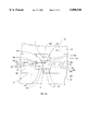
- FIG. 4A is a section view of an MTJ MR read head according to one embodiment of the present invention as it would appear if taken through a plane whose edge is shown as line 42 in FIG. 3 and viewed from the disk surface.
- the paper of FIG. 4A is a plane parallel to the ABS and through substantially the active sensing region, i.e., the tunnel junction, of the MTJ MR read head to reveal the layers that make up the head.
- FIG. 4B is a section view perpendicular to the view of FIG. 4A and with the sensing surface 200 or ABS to the right.
- the MTJ MR read head includes an electrically conductive spacer layer 102 formed directly on the first magnetic shield SI, an electrically conductive spacer layer 104 below and in direct contact with second magnetic shield S2, and the MTJ 100 formed as a stack of layers between electrical spacer layers 102, 104.
- the magnetic shields S1, S2 now serve both as magnetic shields and as the electrically conducting leads for connection of the MTJ 100 to sense circuitry. This is shown in FIG. 4A by the arrows showing the direction of current flow through the first shield S1, perpendicularly through spacer layer 102, MTJ 100, spacer layer 104 and out through the second shield S2.
- the MTJ 100 includes a first electrode multilayer stack 110, an insulating tunnel barrier layer 120, and a top electrode stack 130.
- Each of the electrodes includes a ferromagnetic layer in direct contact with tunnel barrier layer 120, i.e., ferromagnetic layers 118 and 132.
- the base electrode layer stack 110 formed on spacer layer 102 includes a seed or "template” layer 112 on the spacer layer 102, a layer of antiferromagnetic material 116 on the template layer 112, and a "fixed” ferromagnetic layer 118 formed on and exchange coupled with the underlying antiferromagnetic layer 116.
- the ferromagnetic layer 118 is called the fixed layer because its magnetic moment or magnetization direction is prevented from rotation in the presence of applied magnetic fields in the desired range of interest.
- the top electrode stack 130 includes a "free” or “sensing” ferromagnetic layer 132 and a protective or capping layer 134 formed on the sensing layer 132.
- the sensing ferromagnetic layer 132 is not exchange coupled to an antiferromagnetic layer, and its magnetization direction is thus free to rotate in the presence of applied magnetic fields in the range of interest.
- the sensing ferromagnetic layer 132 is fabricated so as to have its magnetic moment or magnetization direction (shown by arrow 133) oriented generally parallel to the ABS (the ABS is a plane parallel to the paper in FIG. 4A and is shown as 200 in FIG. 4B) and generally perpendicular to the magnetization direction of the fixed ferromagnetic layer 118 in the absence of an applied magnetic field.
- the fixed ferromagnetic layer 118 in electrode stack 110 just beneath the tunnel barrier layer 120 has its magnetization direction fixed by interfacial exchange coupling with the immediately underlying antiferromagnetic layer 116, which also forms part of bottom electrode stack 110.
- the magnetization direction of the fixed ferromagnetic layer 118 is oriented generally perpendicular to the ABS, i.e., out of or into the paper in FIG. 4A (as shown by arrow tail 119).
- biasing ferromagnetic layer 150 for longitudinally biasing the magnetization of the sensing ferromagnetic layer 132, and an insulating layer 160 separating and isolating the biasing layer 150 from the sensing ferromagnetic layer 132 and the other layers of the MTJ 100.
- the biasing ferromagnetic layer 150 is not shown in FIG. 4B.
- the biasing ferromagnetic layer 150 is a hard magnetic material, such as a CoPtCr alloy, that has its magnetic moment (shown by arrow 151) aligned in the same direction as the magnetic moment 133 of the sensing ferromagnetic layer 132 in the absence of an applied magnetic field.
- the insulating layer 160 which is preferably alumina (Al 2 O 3 ) or silica (SiO 2 ), has a thickness sufficient to electrically isolate the biasing ferromagnetic layer 150 from the MTJ 100 and the spacer layers 102, 104, but is still thin enough to permit magnetostatic coupling (shown by dashed arrow 153) with the sensing ferromagnetic layer 132.
- the product M*t (where M is the magnetic moment per unit area of the material in the ferromagnetic layer and t is the thickness of the ferromagnetic layer) of the biasing ferromagnetic layer 150 must be greater than or equal to the M*t of the sensing ferromagnetic layer 132 to assure stable longitudinal biasing.
- the thickness of the biasing ferromagnetic layer 150 is at least approximately twice that of the sensing ferromagnetic layer 132.
- a sense current I is directed from the electrically conductive material making up the first shield S1 to first spacer layer 102, perpendicularly through the antiferromagnetic layer 116, the fixed ferromagnetic layer 118, the tunnel barrier layer 120, and the sensing ferromagnetic layer 132 and then to second spacer layer 104 and out through second shield S2.
- the amount of tunneling current through the tunnel barrier layer 120 is a function of the relative orientations of the magnetizations of the fixed and sensing ferromagnetic layers 118, 132 that are adjacent to and in contact with the tunnel barrier layer 120.
- the magnetic field from the recorded data causes the magnetization direction of sensing ferromagnetic layer 132 to rotate away from the direction 133, i.e., either into or out of the paper of FIG. 4A.
- This change in resistance is detected by the disk drive electronics and processed into data read back from the disk.
- the sense current through shields S1 and S2 is prevented from reaching the biasing ferromagnetic layer 150 by the electrical insulating layer 160, which also insulates the biasing ferromagnetic layer 150 from the MTJ 100 and the spacer layers 102, 104.
- a representative set of materials for MTJ 100 (FIGS. 4A-4B) will now be described. All of the layers of the MTJ 100 are grown in the presence of a magnetic field applied parallel to the surface of the substrate. The magnetic field serves to orient the easy axis of all of the ferromagnetic layers.
- a 5 nm Ta seed layer (not shown) is first formed on a 10-50 nm Culayer that serves as the spacer layer 102.
- spacer layer materials are those which are electrically conducting but since the spacer layers are very thin there is no stringent requirement on the value of the conductivity. Thus metals much less conducting than Cu can be used provided that they form suitable layers with the appropriate degree of smoothness on which to subsequently grow the various thin layers which comprise the MTJ device 100.
- the seed layer is comprised of a material which encourages the (111) growth of the face-centered cubic (fcc) Ni 81 Fe 19 template layer 112.
- the template ferromagnetic layer 112 enhances the growth of the antiferromagnetic layer 116.
- Suitable seed layer materials include fcc metals, such as Cu, as well as Ta or a combination of layers, such as 3-5 nm Ta/3-5 nm Cu.
- the MTJ base electrode stack 110 comprises a stack of 4 nm Ni 81 Fe 19 /10 nm Fe 50 Mn 50 /8 nm Ni 81 Fe 19 (layers 112, 116, 118, respectively) grown on the Ta seed layer on the 10-20 nm Cu layer 102.
- the Cu spacer layer 102 is formed directly on the material forming first shield S1 that serves as the substrate.
- the tunnel barrier layer 120 is formed by depositing and then plasma oxidizing a 0.5-2 nm Al layer. This creates the Al 2 O 3 insulating tunnel barrier layer 120.
- the top electrode stack 130 is a 5 nm Ni--Fe/10 nm Ta stack (layers 132, 134, respectively).
- the Ta layer 134 serves as a capping layer for protection of the MTJ 100 during processing.
- the top electrode stack 130 is contacted by a 20 nm Au layer that serves as the spacer layer 104.
- the layers in the bottom electrode stack 110 be smooth, and that the Al 2 O 3 tunnel barrier layer 120 be free of pinholes which would electrically short the junction.
- growth by sputtering techniques known to produce good giant magnetoresistance effects in metallic multilayer stacks is sufficient.
- An alternative sensing ferromagnetic layer 132 may be comprised of a thin Co or Co.sub.(100-x) Fe.sub.(x) (x is approximately 70) or Ni.sub.(100-x) Fe x (x is approximately 60) layer at the interface between the sensing ferromagnetic layer 132 and the tunnel barrier layer 120, with the bulk of layer 132 being a low magnetostriction material, such as Ni.sub.(100-x) Fe x (x is approximately 19).
- the net magnetostriction of this type of sensing layer with a thin Co or Co.sub.(100-x) Fe.sub.(x) (x is approximately 70) or Ni.sub.(100-x) Fe x (x is approximately 60) interface layer is arranged to have a value close to zero by slight variations of the composition of the bulk of layer 132.
- An alternative fixed ferromagnetic layer 118 may be comprised largely of a bulk Ni.sub.(100-x) Fe.sub.(x) (x is approximately 19) layer with a thin layer of a Co or Co.sub.(100-x) Fe.sub.(x) (x is approximately 70) or Ni.sub.(100-x) Fe x (x is approximately 60) layer at the interface with the tunnel barrier layer 120.
- the largest signal is obtained with Co or with the highest polarization Ni.sub.(100-x) Fe x (x is approximately 60) or Co.sub.(100-x) Fe.sub.(x) alloy (x is approximately 70).
- the interface layer is optimally about 1-2 nm thick.
- the net magnetostriction of the combined layer is arranged to be close to zero by small variations of the composition. If the bulk of layer 118 is Ni--Fe, then the composition is Ni 81 Fe 19 , the composition for which bulk Ni--Fe has zero magnetostriction.
- the Fe--Mn antiferromagnetic layer 116 may be replaced with a Ni--Mn layer or other suitable antiferromagnetic layer which exchange biases the ferromagnetic material in the fixed layer 118 and which has a resistance which is substantially less than that of the Al 2 O 3 barrier layer 120.
- the fixed ferromagnetic layer has its magnetic moment fixed by interfacial exchange coupling with an antiferromagnetic layer
- the fixed ferromagnetic layer may be formed of a magnetically "hard" high coercivity material, thereby avoiding the need for an antiferromagnetic layer.
- the MTJ device described and shown in FIGS. 4A-4B has the fixed ferromagnetic layer on the bottom of MTJ 100
- the device can also be formed by depositing the sensing ferromagnetic layer first, followed by the tunnel barrier layer, the fixed ferromagnetic layer, and the antiferromagnetic layer. Such an MTJ device would then have the layers essentially inverted from the MTJ 100 shown in FIGS. 4A-4B.
- the MTJ 100 and its associated spacer layers 102, 104 are placed directly between the magnetic shields S1, S2, as shown in FIGS. 4A-4B, without the need for separate electrical lead layers and insulating gap material to separate the leads from the shields.
- the magnetic shields which are comprised of relatively thick highly permeable magnetic layers, allow the MR sensor to detect individual magnetic transitions without interference from neighboring transitions. Thus the MR sensor can detect magnetic bits with smaller bit lengths than otherwise would possible.
- the resolution of the MR sensor is determined by the separation s between the magnetic shield layers S1 and S2 (see FIG. 4B) and the distance between the sensing surface 200 and the magnetic film on the disk.
- the shields S1 and S2 must be electrically conducting and of suitably high magnetic permeability.
- the shields may be formed from various NiFeX alloys (where X is Ta, Rh, Pt, or Nb) or with CoZrNb alloys or with sendust (FeAlSi) alloys.
- the present invention allows the separation s to be reduced in thickness by the combined thicknesses of the insulating gap layers G1 and G2 (FIG. 3) which were used to electrically isolate the MR sensor.
- the spacing s may of course be reduced further in thickness by reducing the thicknesses of the spacer layers 102 and 104. While in principle any resistance in series with the MTJ device will reduce the magnitude of the signal of the MTJ device the resistance of the spacer layers 102 and 104 in the MTJ MR read head of the present invention is negligible.
- the thickness of a typical MTJ device 100 is ⁇ 66 nm (comprised of layers of 5 nm Ta+15 nm Pt+4 nm Ni 81 Fe 19 +10 nm Fe 50 Mn 50 +6 nm Ni 81 Fe 19 +1 nm Al 2 O 3 +5 nm Ni 81 Fe 19 +20 nm Ta).
- the minimum thicknesses of the insulating gap layers G1, G2 may be ⁇ 20 nm each.
- the separation between S1 and S2 is ⁇ 106 nm.
- the spacer layers 102, 104 are connected directly to the respective shields S1, S2 the gap layers G1 and G2 are removed and the separation between the shields will be reduced to ⁇ 66 nm.
- the linear resolution of the MR head will thus be increased to ⁇ 400,000 transitions per inch.
- the spacing distance s can be optimized to design the MTJ MR read head to operate at the desired linear resolution.
- the MTJ MR read head of the present invention is suitable for ultra dense magnetic recording applications.
- a structure comprised of 2 nm thick Cu spacer layers 102 and 104, a 5 nm thick IrMn exchange bias layer 116, a 2.5 nm thick Co fixed ferromagnetic layer 118, a 1 nm thick Al 2 O 3 tunneling barrier 120 and a 3 nm thick free Ni 81 Fe 19 free ferromagnetic layer
- a MTJ device and spacer layers with a combined thicknes of only 13.5 nm thick can be formed.
- linear densities exceeding 1,500,000 transitions per inch are made possible.
- the free ferromagnetic layer 132 can not be in direct contact with the magnetic shield S2 since the magnetic moment of this layer will then be fixed by exchange coupling to the magnetic moment of the shield and thus will not be able to respond optimally to the flux from the magnetic transitions in the magnetic disk medium.
- the antiferromagnetic exchange bias layer 116 not be in direct contact with the shield S1 since the magnetic properties of the shield will be altered. In particular the magnetic permeability of the shield will be reduced in the region of the antiferromagnetic layer.
- the spacer layers 102, 104 provide electrical connection with layers 116, 132, respectively, while isolating these layers from the shields S1,S2.
- the template layer 112 in contact with the antiferromagnetic layer 116 and the capping layer 134 in contact with the free ferromagnetic layer 132 may serve as spacer layers if made of appropriate materials and formed to suitable thicknesses.
- both the spacer layer 102 and the template 112 may be formed of Ta with a combined thickness of 5-10 nm.
- both layers 134 and 104 may be formed from Ta with a combined thickness of 5-10 nm.
- the combined thickness of the MTJ device 100 and the thicknesses of the spacer layers 102, 104 determines the separation distance s.
- each shield S1, S2 has a respective pedestal 161, 163 in the region where the MTJ 100 is formed so that the spacing s in this region can be made smaller than the spacing s' between the shields outside the region where the MTJ 100 is formed. In this manner the larger distance s' decreases the likelihood of an electrical short between the two shields S1, S2.
- Another advantage of the MTJ MR read head of the present invention is that the electrical resistance of the shields which now also act as the electrical leads to the MTJ device is small because the shields are very thick.
- these leads must be formed from thin conducting layers and separated from the shields by additional insulating layers.
- the shield to shield separation s must be kept small which limits the thickness of the electrical leads in the vicinity of the MTJ device.
- the voltage drop across the shields which now also act as the electrical leads is small.
- FIGS. 6A-6E the process for forming the MTJ MR read head of the present invention will be described.
- a process will be described for forming an MTJ MR head similar to that shown in FIG. 6, where the separation between the magnetic shields is greater in the region away from the MTJ device.
- the forming of the longitudinal bias regions 150 shown in FIG. 4A will not be described.
- the process begins, as shown in FIG. 6A, by depositing the material for spacer layer layer 102, the MTJ device 100 and the top spacer layer 104 on top of the shield S1.
- the spacer layer material 102 can be of a variety of conducting materials, such as Ta, Al, Cu, Au, W and Pt with a typical thickness in the range of 0 to 20 nm.
- the antiferromagnetic layer 116 can be selected from a variety of well-known materials, such as Fe--Mn, Ni--Mn, Pt--Mn, Ir--Mn and Pd--Mn.
- the typical thickness for the antiferromagnetic layer 116 is in the range of 7 to 30 nm.
- the fixed ferromagnetic layer 118 is preferably a Ni--Fe alloy or a bilayer of Ni--Fe alloy and a thin film of Co. Typical thicknesses for the Ni--Fe alloy layer are 2 to 10 nm and typical thicknesses for the Co layer are 0.2 to 2 nm.
- the thickness of the aluminum the tunnel barrier oxide layer 120 is typically in the range of 0.5 to 1.5 nm.
- the free ferromagnetic layer 132 is typically a Ni--Fe alloy or a bilayer of Co and a Ni--Fe alloy, with a thickness from 10 to 20 nm for the Ni--Fe alloy and a thickness of 0.2 to 2 nm for the Co.
- the spacer layer 104 is formed of similar materials and thicknesses as described for the spacer layer 102.
- the layers are lithographically patterned using the resist 230 shown in FIG. 6B. Ion milling then removes material not protected by the resist 230, as shown in FIG. 6C.
- the ion milling procedure is designed such that by choosing suitable conditions such as the time of the ion milling not only are the layers 102, 100 and 104 removed everywhere there is no resist 230 but in addition material is removed from the the top surface of the bottom shield S1 to a depth d.
- the resist layer 230 is typically a bilayer resist with an undercut.
- a layer 250 of insulating material is deposited by ion beam or RF sputtering to a thickness which is greater than at least the sum of d and the thicknesses of the spacer layer 102 and the MTJ device 100 and the spacer layer 104, as shown in FIG. 6D.
- the resist layer 230 is lifted off, removing the insulating material 250 that was deposited on top of the spacer layer 104.
- the top shield layer S2 is formed by either ion beam deposition or RF or DC magnetron sputtering, as shown in FIG. 6E.
- the above process can also be adapted to provide longitudinal biasing or stabilization for the free ferromagnetic layer 132 by incorporation of the hard magnetic material in regions 150, as shown in FIG. 4A.
- the total thickness of the spacer layers, free and fixed ferromagnetic layer, tunnel oxide layer, and antiferromagnetic layer may be in the range 50-80 nm.
- the lower shield S1 may be overmilled by a thickness d ⁇ 30 nm and the thickness of the insulating layer deposited in the step of FIG. 6D may be ⁇ 120 nm.
- this example using the fabrication sequence described in FIGS. 6A-6E leads to a MTJ MR read head with a resolution gap s of ⁇ 50-80 nm but a shield to shield s' separation away from the MTJ sensor of ⁇ 120 nm rather than 50-80 nm.
- the MTJ sensor After the definition and fabrication of the MTJ sensor it is still necessary to align the magnetization direction (magnetic moment) of the fixed ferromagnetic layer 118 in the proper direction.
- Fe--Mn is used as the antiferromagnetic layer 116 for exchange coupling with the fixed ferromagnetic layer 118 it is antiferromagnetic as deposited. However, its magnetization must be realigned so that it can exchange couple the fixed ferromagnetic layer 118 in the proper orientation.
- the structure is placed in an annealing oven and the temperature is raised to approximately 180° C., which is greater than the blocking temperature of Fe--Mn. At this temperature, the Fe--Mn layer no longer gives rise to an exchange anisotropy with the fixed ferromagnetic layer 118.
- An exchange anisotropy of the ferromagnetic layer 118 is developed by cooling the pair of layers 116, 118 in a magnetic field.
- the orientation of the magnetization of the fixed ferromagnetic layer 118 will be along the direction of the applied magnetic field.
- the applied magnetic field in the annealing oven thus causes the moment of the fixed ferromagnetic layer 118 to be fixed along the required direction perpendicular to the ABS, as shown by the arrow 119 in FIG. 4A.
- This is a result of cooling the Fe--Mn layer in the presence of the ferromagnetic layer 118, magnetized by the applied magnetic field, in the required direction.
- the magnetization of the fixed ferromagnetic layer 118 will not substantially rotate.
- While the embodiment of the present invention described in FIG. 5 has pedestals 161, 163 of the same area as the area of the MTJ device 100 and aligned with the MTJ device this is not a necessary requirement.
- the area of the pedestals can be made larger than the area of the MTJ device 100 and the MTJ device does not have to be centered within the pedestals although the boundaries of the MTJ device must lie within the area of the pedestals.
- only one pedestal on either side of the MTJ device is required to allow for increased separation of the shields S1, S2 away from the MTJ device.
- Such an alternative embodiment with only the upper pedestal may be formed by a similar process of fabrication as described in FIGS. 6A-6E.
- the MTJ device 100 and spacer layers 102 and 104 are not overmilled as shown in FIG. 6C but are milled through only as far as the surface of the shield S1. Thus no lower pedestal is formed. The rest of the process is otherwise identical.
- An embodiment in which only the lower pedestal is formed is fabricated by a similar set of fabrication steps as shown in FIGS. 6A-6E except that except that after removing the photoresist 230 after step FIG. 6D the resulting surface of the device is planarized by a process of chemical mechanical polishing. The shield S2 is then directly deposited on the planarized surface and no upper pedestal is formed.
Abstract
Description
Claims (26)
Priority Applications (9)
| Application Number | Priority Date | Filing Date | Title |
|---|---|---|---|
| US08/957,787 US5898548A (en) | 1997-10-24 | 1997-10-24 | Shielded magnetic tunnel junction magnetoresistive read head |
| KR1019980037936A KR100295288B1 (en) | 1997-10-24 | 1998-09-15 | Shielded magnetic tunnel junction magnetoresistive read head |
| MYPI98004347A MY116285A (en) | 1997-10-24 | 1998-09-22 | Shielded magnetic tunnel junction magnetoresistive read head |
| CNB981194036A CN1144183C (en) | 1997-10-24 | 1998-09-30 | Shielded magnetic tunnel junction magnetoresistive read head |
| JP28902098A JP3300291B2 (en) | 1997-10-24 | 1998-10-12 | Shielded magnetic tunnel junction magnetoresistive read head and assembly |
| SG1998004212A SG67574A1 (en) | 1997-10-24 | 1998-10-15 | Shielded magnetic tunnel junction magnetoresistive read head |
| EP98308587A EP0911811B1 (en) | 1997-10-24 | 1998-10-20 | Shielded magnetic tunnel junction magnetoresistive read head |
| DE69835410T DE69835410T2 (en) | 1997-10-24 | 1998-10-20 | Magnetoresistive read head with shielded magnetic tunnel junction |
| JP2001389357A JP2002304711A (en) | 1997-10-24 | 2001-12-21 | Shielded magnetic tunnel junction magneto-resistive read head and assembly |
Applications Claiming Priority (1)
| Application Number | Priority Date | Filing Date | Title |
|---|---|---|---|
| US08/957,787 US5898548A (en) | 1997-10-24 | 1997-10-24 | Shielded magnetic tunnel junction magnetoresistive read head |
Publications (1)
| Publication Number | Publication Date |
|---|---|
| US5898548A true US5898548A (en) | 1999-04-27 |
Family
ID=25500133
Family Applications (1)
| Application Number | Title | Priority Date | Filing Date |
|---|---|---|---|
| US08/957,787 Expired - Lifetime US5898548A (en) | 1997-10-24 | 1997-10-24 | Shielded magnetic tunnel junction magnetoresistive read head |
Country Status (8)
| Country | Link |
|---|---|
| US (1) | US5898548A (en) |
| EP (1) | EP0911811B1 (en) |
| JP (2) | JP3300291B2 (en) |
| KR (1) | KR100295288B1 (en) |
| CN (1) | CN1144183C (en) |
| DE (1) | DE69835410T2 (en) |
| MY (1) | MY116285A (en) |
| SG (1) | SG67574A1 (en) |
Cited By (117)
| Publication number | Priority date | Publication date | Assignee | Title |
|---|---|---|---|---|
| US6052263A (en) * | 1998-08-21 | 2000-04-18 | International Business Machines Corporation | Low moment/high coercivity pinned layer for magnetic tunnel junction sensors |
| WO2000028342A1 (en) * | 1998-11-09 | 2000-05-18 | International Business Machines Corporation | Disk drive with thermal asperity reduction circuitry using a magnetic tunnel junction sensor |
| US6084752A (en) * | 1996-02-22 | 2000-07-04 | Matsushita Electric Industrial Co., Ltd. | Thin film magnetic head |
| US6153062A (en) * | 1996-09-12 | 2000-11-28 | Alps Electric Co., Ltd. | Magnetoresistive sensor and head |
| US6178074B1 (en) * | 1998-11-19 | 2001-01-23 | International Business Machines Corporation | Double tunnel junction with magnetoresistance enhancement layer |
| US6181537B1 (en) * | 1999-03-29 | 2001-01-30 | International Business Machines Corporation | Tunnel junction structure with junction layer embedded in amorphous ferromagnetic layers |
| US6256178B1 (en) * | 1999-03-29 | 2001-07-03 | International Business Machines Corporation | Biasing for tunnel junction head |
| US20010033464A1 (en) * | 2000-04-19 | 2001-10-25 | Tdk Corporation | Tunnel magnetoresistive effective element, a thin film magnetic head, a magnetic head device and a magnetic disk drive device |
| US6333842B1 (en) * | 1997-12-05 | 2001-12-25 | Nec Corporation | Magneto-resistance effect type composite head and production method thereof |
| US20020008016A1 (en) * | 2000-05-15 | 2002-01-24 | Kazuhiko Hayashi | Magnetoresistive effect sensor, method for manufacturing a magnetoresistive effect sensor, magnetoresistive detection system, and magnetoresistive recording system |
| US6342993B1 (en) * | 1998-10-13 | 2002-01-29 | Tdk Corporation | Thin film magnetic head and method of manufacturing the same |
| US6344954B1 (en) | 1999-07-02 | 2002-02-05 | Tdk Corporation | Magneto-resistive tunnel junction head with specific flux guide structure |
| US6353318B1 (en) * | 2000-03-10 | 2002-03-05 | Read-Rite Corporation | Magnetoresistive sensor having hard biased current perpendicular to the plane sensor |
| US20020027751A1 (en) * | 2000-07-10 | 2002-03-07 | Koji Shimazawa | Magnetoresistive effect thin-film magnetic head and manufacturing method of magnetoresistive effect thin-film magnetic head |
| US6358635B1 (en) | 1999-12-20 | 2002-03-19 | Headway Technologies, Inc. | Magnetic recording sensor with stabilizing shield |
| US6411478B1 (en) | 1999-02-11 | 2002-06-25 | Seagate Technology Llc | Spin tunnel junction recording heads using an edge junction structure with CIP |
| US6414826B1 (en) * | 2000-02-18 | 2002-07-02 | International Business Machines Corporation | High sensitivity AP pinned head |
| US20020085316A1 (en) * | 2001-01-04 | 2002-07-04 | Richard Hsiao | Magnetic transducer with electrically conductive shield for reducing electromagnetic interference |
| US6421212B1 (en) * | 1999-09-21 | 2002-07-16 | Read-Rite Corporation | Thin film read head structure with improved bias magnet-to-magnetoresistive element interface and method of fabrication |
| US20020114972A1 (en) * | 1998-01-06 | 2002-08-22 | Anthony Thomas C | Ferromagnetic tunnel junctions with enhanced magneto-resistance |
| US6445552B1 (en) * | 2000-02-18 | 2002-09-03 | International Business Machines Corporation | Shield design for stable magnetoresistive head |
| US6466419B1 (en) * | 2000-03-31 | 2002-10-15 | Seagate Technology Llc | Current perpendicular to plane spin valve head |
| US6469874B1 (en) | 2000-03-13 | 2002-10-22 | Headway Technologies, Inc. | Method to make a stitched writer for a giant magneto-resistive head |
| WO2002086871A1 (en) * | 2001-04-18 | 2002-10-31 | Seagate Technology Llc | Non-magnetic metallic layer in a reader gap of a disc drive |
| US6493195B1 (en) * | 1999-09-01 | 2002-12-10 | Nec Corporation | Magnetoresistance element, with lower electrode anti-erosion/flaking layer |
| US6496337B1 (en) * | 2000-03-20 | 2002-12-17 | Headway Technologies, Inc. | Copper alloy GMR recording head |
| US6496334B1 (en) | 2000-05-26 | 2002-12-17 | Read-Rite Corportion | Data storage and retrieval apparatus with thin film read head having planarized extra gap and shield layers and method of fabrication thereof |
| US6501271B1 (en) * | 1998-05-11 | 2002-12-31 | Koninkiljke Philips Electronics N.V. | Robust giant magnetoresistive effect type multilayer sensor |
| US6510030B1 (en) | 1999-08-17 | 2003-01-21 | Seagate Technology, Llc | Transducing head and method for forming a recessed shield for a transducing head |
| US6519124B1 (en) | 2000-03-27 | 2003-02-11 | Tdk Corporation | Magnetic tunnel junction read head using a hybrid, low-magnetization flux guide |
| US20030030948A1 (en) * | 2001-08-13 | 2003-02-13 | Eiji Umetsu | CPP type magnetic sensor or magnetic sensor using tunnel effect, and manufacturing method therefor |
| US20030053266A1 (en) * | 2001-09-17 | 2003-03-20 | Headway Technologies, Inc. | Multilayered structures comprising magnetic nano-oxide layers for current perpendicular to plane GMR heads |
| US6542343B1 (en) | 2000-08-09 | 2003-04-01 | International Business Machines Corporation | Tunnel valve head design to lower resistance |
| US6542340B1 (en) * | 1999-09-01 | 2003-04-01 | Nec Corporation | Magnetoresistance element, manufacturing method thereof, magnetic field detection system and magnetic recording system |
| US6552882B1 (en) * | 1998-09-01 | 2003-04-22 | Nec Corporation | Information reproduction head apparatus and information recording/reproduction system |
| US6556391B1 (en) * | 1999-12-07 | 2003-04-29 | Fujitsu Limited | Biasing layers for a magnetoresistance effect magnetic head using perpendicular current flow |
| US6560077B2 (en) * | 2000-01-10 | 2003-05-06 | The University Of Alabama | CPP spin-valve device |
| US6563679B1 (en) * | 2000-08-08 | 2003-05-13 | Tdk Corporation | Current perpendicular-to-the-plane magnetoresistance read heads with transverse magnetic bias |
| US6567244B1 (en) | 2000-10-10 | 2003-05-20 | Hitachi Global Storage Technologies Netherlands | Differential yoke type read head |
| US20030106616A1 (en) * | 2000-04-12 | 2003-06-12 | Alps Electric Co., Ltd. | Method of producing exchange coupling film and method of producing magnetoresistive sensor by using exchange coupling film |
| US6587318B2 (en) * | 1998-04-30 | 2003-07-01 | Hitachi, Ltd. | Spin tunnel magneto-resistance effect type magnetic sensor and production method thereof |
| US6600636B1 (en) | 1999-10-12 | 2003-07-29 | Maxtor Corporation | Magnetic head with write element offset from read element |
| US20030165034A1 (en) * | 2002-03-01 | 2003-09-04 | Vladimir Nikitin | Reduction of interference pickup in heads for magnetic recording by minimizing parasitic capacitance |
| US6657829B2 (en) | 2000-02-04 | 2003-12-02 | Alps Electric Co., Ltd. | Tunneling magnetoresistive device |
| US6667862B2 (en) | 2001-02-20 | 2003-12-23 | Carnegie Mellon University | Magnetoresistive read head having permanent magnet on top of magnetoresistive element |
| US6671141B2 (en) | 2000-03-17 | 2003-12-30 | Tdk Corporation | Tunnel magnetoresistive effective element, a thin film magnetic head, a magnetic head device and a magnetic disk drive device |
| US6680832B2 (en) * | 2001-05-11 | 2004-01-20 | International Business Machines Corporation | CPP magnetoresistive sensors with in-stack longitudinal biasing and overlapping magnetic shield |
| US6680829B2 (en) | 2000-09-13 | 2004-01-20 | Seagate Technology Llc | MR structures for high areal density reader by using side shields |
| US20040019272A1 (en) * | 2002-07-23 | 2004-01-29 | Honeywell International Inc. | Magnetic sensing device |
| US6700752B2 (en) * | 2001-04-18 | 2004-03-02 | Seagate Technology Llc | Non-magnetic metallic layer in a reader gap of a disc drive |
| US6700759B1 (en) | 2000-06-02 | 2004-03-02 | Western Digital (Fremont), Inc. | Narrow track width magnetoresistive sensor and method of making |
| US20040047083A1 (en) * | 2000-07-17 | 2004-03-11 | Naoya Hasegawa | Tunneling magneoresistive element and method of manufacturing the same |
| US6721147B2 (en) | 1999-12-07 | 2004-04-13 | Fujitsu Limited | Longitudinally biased magnetoresistance effect magnetic head and magnetic reproducing apparatus |
| US20040080873A1 (en) * | 2002-10-29 | 2004-04-29 | Taku Shintani | Magnetic sensor |
| US6738234B1 (en) * | 2000-03-15 | 2004-05-18 | Tdk Corporation | Thin film magnetic head and magnetic transducer |
| US6744608B1 (en) * | 2002-05-14 | 2004-06-01 | Western Digital (Fremont), Inc. | Method and system for making TMR junctions |
| US6781801B2 (en) | 2001-08-10 | 2004-08-24 | Seagate Technology Llc | Tunneling magnetoresistive sensor with spin polarized current injection |
| US6795280B1 (en) | 1998-11-18 | 2004-09-21 | Seagate Technology Llc | Tunneling magneto-resistive read head with two-piece free layer |
| US6798621B2 (en) | 2002-08-15 | 2004-09-28 | International Business Machines Corporation | Shield electrical connections for tunnel valve sensors |
| US6801408B1 (en) | 2000-11-02 | 2004-10-05 | Western Digital (Fremont), Inc. | Data storage and retrieval apparatus with thin film read head having a planar sensor element and an extra gap and method of fabrication thereof |
| US20040207959A1 (en) * | 2003-04-18 | 2004-10-21 | Alps Electric Co., Ltd. | CPP giant magnetoresistive head with large-area metal film provided between shield and element |
| US20040207960A1 (en) * | 2003-04-18 | 2004-10-21 | Alps Electric Co., Ltd. | Self-pinned CPP giant magnetoresistive head with antiferromagnetic film absent from current path |
| US20040212932A1 (en) * | 2003-04-24 | 2004-10-28 | Tdk Corporation | Magnetoresistive effective element, thin film magnetic head, magnetic head device and magnetic recording/reproducing device |
| US20040223267A1 (en) * | 2002-06-17 | 2004-11-11 | Childress Jeffrey R. | Current-perpendicular-to-plane magnetoresistive device with oxidized free layer side regions and method for its fabrication |
| US6819530B2 (en) | 2002-09-25 | 2004-11-16 | International Business Machines Corporation | Current perpendicular to the planes (CPP) sensor with free layer stabilized by current field |
| US6847510B2 (en) | 2002-09-27 | 2005-01-25 | Hitachi Global Storage Technologies Netherlands B.V. | Magnetic tunnel junction device with bottom free layer and improved underlayer |
| US20050063104A1 (en) * | 2003-09-02 | 2005-03-24 | Kabushiki Kaisha Toshiba | Magnetic recording/reproducing apparatus |
| US6873502B2 (en) * | 2000-07-06 | 2005-03-29 | Sony Corporation | Magnetic tunnel effect type magnetic head, and method of producing same |
| US6888184B1 (en) * | 2001-02-23 | 2005-05-03 | Western Digital (Fremont), Inc. | Shielded magnetic ram cells |
| US20050110004A1 (en) * | 2003-11-24 | 2005-05-26 | International Business Machines Corporation | Magnetic tunnel junction with improved tunneling magneto-resistance |
| US20050163037A1 (en) * | 2000-07-25 | 2005-07-28 | Seagate Technology Llc | Magnetic anisotropy of soft-underlayer induced by magnetron field |
| US20050168877A1 (en) * | 2003-03-06 | 2005-08-04 | Fujitsu Limited | Magnetoresistive head |
| US20050188166A1 (en) * | 2001-08-10 | 2005-08-25 | Hitachi, Ltd. | Apparatus and method for online data migration with remote copy |
| US6950290B2 (en) * | 1998-11-30 | 2005-09-27 | Nec Corporation | Magnetoresistive effect transducer having longitudinal bias layer directly connected to free layer |
| US20050219765A1 (en) * | 2004-04-02 | 2005-10-06 | Tdk Corporation | Composite type thin-film magnetic head |
| US20060002022A1 (en) * | 2004-06-30 | 2006-01-05 | Michael Feldbaum | Magnetic head for hard disk drive having improved magnetic shield for MR sensor |
| US20060067014A1 (en) * | 2004-09-29 | 2006-03-30 | Hitachi Global Storage Technologies | Magnetoresistive sensor having a high coercivity hard magnetic bias layer deposited over a metallic layer |
| US20060067015A1 (en) * | 2004-09-29 | 2006-03-30 | Hitachi Global Storgage Technologies | Magnetic sensor having a seedlayer for providing improved hard magnet properties |
| US20060171069A1 (en) * | 2005-01-31 | 2006-08-03 | Hitachi Global Storage Technologies Netherlands B.V. | P1 write pole with shoulder formation and method of fabrication |
| US20060250726A1 (en) * | 2005-05-09 | 2006-11-09 | Hitachi Global Storage Technologies Netherlands B. V. | Shield structure in magnetic recording heads |
| US20060256481A1 (en) * | 2005-05-13 | 2006-11-16 | Tdk Corporation | Composite thin-film magnetic head, magnetic head assembly and magnetic disk drive apparatus |
| US20060279877A1 (en) * | 2005-06-14 | 2006-12-14 | Dian Song | Head to disc interface tunneling giant magnetoresistive sensor |
| US20070115595A1 (en) * | 2005-11-18 | 2007-05-24 | Alps Electric Co., Ltd. | Cpp-type thin-film magnetic head and manufacturing method thereof |
| US20070223147A1 (en) * | 2003-08-07 | 2007-09-27 | Tdk Corporation | Method of manufacturing thin-film magnetic head |
| US20080002307A1 (en) * | 2006-06-30 | 2008-01-03 | Fujitsu Limited | Thin film magnetic head and method of producing the same |
| US7356909B1 (en) | 2004-09-29 | 2008-04-15 | Headway Technologies, Inc. | Method of forming a CPP magnetic recording head with a self-stabilizing vortex configuration |
| CN100446086C (en) * | 2004-09-03 | 2008-12-24 | 株式会社东芝 | Magnetoresistive element, magnetic head, magnetic recording apparatus, and magnetic memory |
| US20090168214A1 (en) * | 2007-12-27 | 2009-07-02 | Satoru Araki | Verification of a fabrication process used to form read elements in magnetic heads |
| US20090168256A1 (en) * | 2007-12-27 | 2009-07-02 | Daniele Mauri | Magnetoresistance (mr) read elements having an active shield |
| US20110069413A1 (en) * | 2009-09-23 | 2011-03-24 | Hitachi Global Storage Technologies Netherlands B.V. | Current-perpendicular-to-the-plane (cpp) magnetoresistive read head with multiple sensing elements for patterned-media |
| US20130176022A1 (en) * | 2012-01-09 | 2013-07-11 | Voltafield Technology Corporation | Magnetoresistive sensing device |
| US20130265039A1 (en) * | 2012-02-10 | 2013-10-10 | Memsic, Inc. | Planar three-axis magnetometer |
| US20140197827A1 (en) * | 2013-01-15 | 2014-07-17 | Infineon Technologies Ag | XMR-Sensor and Method for Manufacturing the XMR-Sensor |
| US20150269955A1 (en) * | 2014-03-24 | 2015-09-24 | Kabushiki Kaisha Toshiba | Magnetic head, magnetic head assembly, and magnetic recording apparatus |
| US9263068B1 (en) | 2014-11-05 | 2016-02-16 | International Business Machines Corporation | Magnetic read head having a CPP MR sensor electrically isolated from a top shield |
| US9280991B1 (en) | 2015-01-07 | 2016-03-08 | International Business Machines Corporation | TMR head design with insulative layers for shorting mitigation |
| US9373779B1 (en) | 2014-12-08 | 2016-06-21 | Micron Technology, Inc. | Magnetic tunnel junctions |
| US9431600B2 (en) * | 2014-10-06 | 2016-08-30 | International Business Machines Corporation | Magnetic domain wall shift register memory devices with high magnetoresistance ratio structures |
| US9437267B2 (en) | 2011-11-30 | 2016-09-06 | Sony Corporation | Storage element and memory |
| US9502642B2 (en) * | 2015-04-10 | 2016-11-22 | Micron Technology, Inc. | Magnetic tunnel junctions, methods used while forming magnetic tunnel junctions, and methods of forming magnetic tunnel junctions |
| US9520553B2 (en) | 2015-04-15 | 2016-12-13 | Micron Technology, Inc. | Methods of forming a magnetic electrode of a magnetic tunnel junction and methods of forming a magnetic tunnel junction |
| US9530959B2 (en) | 2015-04-15 | 2016-12-27 | Micron Technology, Inc. | Magnetic tunnel junctions |
| US9553259B2 (en) | 2015-05-05 | 2017-01-24 | Micron Technology, Inc. | Magnetic tunnel junctions |
| US9596995B2 (en) | 2013-06-12 | 2017-03-21 | Kabushiki Kaisha Toshiba | Pressure sensor, acoustic microphone, blood pressure sensor, and touch panel |
| US9607635B1 (en) | 2016-04-22 | 2017-03-28 | International Business Machines Corporation | Current perpendicular-to-plane sensors having hard spacers |
| US9680089B1 (en) | 2016-05-13 | 2017-06-13 | Micron Technology, Inc. | Magnetic tunnel junctions |
| US9691817B2 (en) | 2013-09-10 | 2017-06-27 | Micron Technology, Inc. | Magnetic tunnel junctions and methods of forming magnetic tunnel junctions |
| US9853209B2 (en) | 2014-03-19 | 2017-12-26 | Kabushiki Kaisha Toshiba | Method of manufacturing pressure sensor, deposition system, and annealing system |
| US9947348B1 (en) | 2017-02-28 | 2018-04-17 | International Business Machines Corporation | Tunnel magnetoresistive sensor having leads supporting three-dimensional current flow |
| US9960346B2 (en) | 2015-05-07 | 2018-05-01 | Micron Technology, Inc. | Magnetic tunnel junctions |
| US9997180B1 (en) | 2017-03-22 | 2018-06-12 | International Business Machines Corporation | Hybrid dielectric gap liner and magnetic shield liner |
| US20190027679A1 (en) * | 2016-03-30 | 2019-01-24 | Intel Corporation | Approaches for strain engineering of perpendicular magnetic tunnel junctions (pmtjs) and the resulting structures |
| US10448845B2 (en) | 2013-09-20 | 2019-10-22 | Kabushiki Kaisha Toshiba | Strain sensing element, having a first and second magnetic layer and a third layer that is antiferrimagnetic |
| US10714125B2 (en) * | 2018-05-14 | 2020-07-14 | Sandisk Technologies Llc | Method of manufacturing a magnetic recording head |
| US10803889B2 (en) | 2019-02-21 | 2020-10-13 | International Business Machines Corporation | Apparatus with data reader sensors more recessed than servo reader sensor |
| US11074930B1 (en) | 2020-05-11 | 2021-07-27 | International Business Machines Corporation | Read transducer structure having an embedded wear layer between thin and thick shield portions |
| US11114117B1 (en) | 2020-05-20 | 2021-09-07 | International Business Machines Corporation | Process for manufacturing magnetic head having a servo read transducer structure with dielectric gap liner and a data read transducer structure with an embedded wear layer between thin and thick shield portions |
Families Citing this family (11)
| Publication number | Priority date | Publication date | Assignee | Title |
|---|---|---|---|---|
| JP2001176027A (en) | 1999-12-14 | 2001-06-29 | Nec Corp | Magnetoresistance effect head and magnetic memory device using the same |
| US6359289B1 (en) * | 2000-04-19 | 2002-03-19 | International Business Machines Corporation | Magnetic tunnel junction device with improved insulating tunnel barrier |
| JP2002025017A (en) | 2000-07-10 | 2002-01-25 | Tdk Corp | Magnetoresistance effect thin film magnetic head |
| JP2003178407A (en) | 2001-12-11 | 2003-06-27 | Hitachi Ltd | Magneto-resistance effect type head, its manufacturing method, and magnetic recording/reproducing device |
| FR2852400B1 (en) * | 2003-03-14 | 2005-06-24 | MAGNETORESISTIVE SENSOR COMPRISING A SENSITIVE FERROMAGNETIC / ANTIFERROMAGNETIC ELEMENT | |
| US6929957B2 (en) * | 2003-09-12 | 2005-08-16 | Headway Technologies, Inc. | Magnetic random access memory designs with patterned and stabilized magnetic shields |
| US7463459B2 (en) * | 2004-02-18 | 2008-12-09 | Hitachi Global Storage Technologies Netherlands B.V. | Self-pinned read sensor design with enhanced lead stabilizing mechanism |
| US8336194B2 (en) * | 2009-11-03 | 2012-12-25 | Western Digital (Fremont), Llc | Method of fabricating a tunneling magnetoresistive (TMR) reader |
| US9001473B1 (en) * | 2014-03-21 | 2015-04-07 | HGST Netherlands B.V. | TMR/CPP reader for narrow reader gap application |
| WO2015182645A1 (en) * | 2014-05-30 | 2015-12-03 | 株式会社村田製作所 | Magnetoresistive element, magnetic sensor and current sensor |
| US9747931B1 (en) | 2016-08-16 | 2017-08-29 | International Business Machines Corporation | Tunnel magnetoresistive sensor having stabilized magnetic shield and dielectric gap sensor |
Citations (7)
| Publication number | Priority date | Publication date | Assignee | Title |
|---|---|---|---|---|
| US5390061A (en) * | 1990-06-08 | 1995-02-14 | Hitachi, Ltd. | Multilayer magnetoresistance effect-type magnetic head |
| US5432734A (en) * | 1993-08-30 | 1995-07-11 | Mitsubishi Denki Kabushiki Kaisha | Magnetoresistive element and devices utilizing the same |
| US5629922A (en) * | 1995-02-22 | 1997-05-13 | Massachusetts Institute Of Technology | Electron tunneling device using ferromagnetic thin films |
| US5650958A (en) * | 1996-03-18 | 1997-07-22 | International Business Machines Corporation | Magnetic tunnel junctions with controlled magnetic response |
| US5712612A (en) * | 1996-01-02 | 1998-01-27 | Hewlett-Packard Company | Tunneling ferrimagnetic magnetoresistive sensor |
| US5729410A (en) * | 1996-11-27 | 1998-03-17 | International Business Machines Corporation | Magnetic tunnel junction device with longitudinal biasing |
| US5747859A (en) * | 1995-09-01 | 1998-05-05 | Kabushiki Kaisha Toshiba | Magnetic device and magnetic sensor using the same |
Family Cites Families (3)
| Publication number | Priority date | Publication date | Assignee | Title |
|---|---|---|---|---|
| EP0768642A3 (en) * | 1995-10-13 | 1998-12-16 | Read-Rite Corporation | Magnetic head with biased GMR element and sense current compensation |
| EP0782129A3 (en) * | 1995-12-29 | 1998-12-09 | Read-Rite Corporation | Magnetoresistive cpp mode transducer with multiple spin valve members |
| US6084752A (en) * | 1996-02-22 | 2000-07-04 | Matsushita Electric Industrial Co., Ltd. | Thin film magnetic head |
-
1997
- 1997-10-24 US US08/957,787 patent/US5898548A/en not_active Expired - Lifetime
-
1998
- 1998-09-15 KR KR1019980037936A patent/KR100295288B1/en not_active IP Right Cessation
- 1998-09-22 MY MYPI98004347A patent/MY116285A/en unknown
- 1998-09-30 CN CNB981194036A patent/CN1144183C/en not_active Expired - Fee Related
- 1998-10-12 JP JP28902098A patent/JP3300291B2/en not_active Expired - Fee Related
- 1998-10-15 SG SG1998004212A patent/SG67574A1/en unknown
- 1998-10-20 EP EP98308587A patent/EP0911811B1/en not_active Expired - Lifetime
- 1998-10-20 DE DE69835410T patent/DE69835410T2/en not_active Expired - Fee Related
-
2001
- 2001-12-21 JP JP2001389357A patent/JP2002304711A/en active Pending
Patent Citations (8)
| Publication number | Priority date | Publication date | Assignee | Title |
|---|---|---|---|---|
| US5390061A (en) * | 1990-06-08 | 1995-02-14 | Hitachi, Ltd. | Multilayer magnetoresistance effect-type magnetic head |
| US5726837A (en) * | 1990-06-08 | 1998-03-10 | Hitachi, Ltd. | Multilayer magnetoresistance effect-type magnetic head |
| US5432734A (en) * | 1993-08-30 | 1995-07-11 | Mitsubishi Denki Kabushiki Kaisha | Magnetoresistive element and devices utilizing the same |
| US5629922A (en) * | 1995-02-22 | 1997-05-13 | Massachusetts Institute Of Technology | Electron tunneling device using ferromagnetic thin films |
| US5747859A (en) * | 1995-09-01 | 1998-05-05 | Kabushiki Kaisha Toshiba | Magnetic device and magnetic sensor using the same |
| US5712612A (en) * | 1996-01-02 | 1998-01-27 | Hewlett-Packard Company | Tunneling ferrimagnetic magnetoresistive sensor |
| US5650958A (en) * | 1996-03-18 | 1997-07-22 | International Business Machines Corporation | Magnetic tunnel junctions with controlled magnetic response |
| US5729410A (en) * | 1996-11-27 | 1998-03-17 | International Business Machines Corporation | Magnetic tunnel junction device with longitudinal biasing |
Cited By (190)
| Publication number | Priority date | Publication date | Assignee | Title |
|---|---|---|---|---|
| US6400537B2 (en) * | 1996-02-22 | 2002-06-04 | Matsushita Electric Industrial Co., Ltd. | Thin film magnetic head |
| US6084752A (en) * | 1996-02-22 | 2000-07-04 | Matsushita Electric Industrial Co., Ltd. | Thin film magnetic head |
| US6352621B1 (en) | 1996-09-12 | 2002-03-05 | Alps Electric Co., Ltd. | Method of manufacturing film laminate having exchange anisotropic magnetic field |
| US6153062A (en) * | 1996-09-12 | 2000-11-28 | Alps Electric Co., Ltd. | Magnetoresistive sensor and head |
| US6333842B1 (en) * | 1997-12-05 | 2001-12-25 | Nec Corporation | Magneto-resistance effect type composite head and production method thereof |
| US6639766B2 (en) | 1997-12-05 | 2003-10-28 | Nec Corporation | Magneto-resistance effect type composite head and production method thereof |
| US6511855B2 (en) * | 1998-01-06 | 2003-01-28 | Hewlett-Packard Company | Method of forming ferromagnetic tunnel junctions with enhanced magneto-resistance |
| US20020114972A1 (en) * | 1998-01-06 | 2002-08-22 | Anthony Thomas C | Ferromagnetic tunnel junctions with enhanced magneto-resistance |
| US6587318B2 (en) * | 1998-04-30 | 2003-07-01 | Hitachi, Ltd. | Spin tunnel magneto-resistance effect type magnetic sensor and production method thereof |
| US6501271B1 (en) * | 1998-05-11 | 2002-12-31 | Koninkiljke Philips Electronics N.V. | Robust giant magnetoresistive effect type multilayer sensor |
| US6052263A (en) * | 1998-08-21 | 2000-04-18 | International Business Machines Corporation | Low moment/high coercivity pinned layer for magnetic tunnel junction sensors |
| US6552882B1 (en) * | 1998-09-01 | 2003-04-22 | Nec Corporation | Information reproduction head apparatus and information recording/reproduction system |
| US6342993B1 (en) * | 1998-10-13 | 2002-01-29 | Tdk Corporation | Thin film magnetic head and method of manufacturing the same |
| US6185079B1 (en) | 1998-11-09 | 2001-02-06 | International Business Machines Corporation | Disk drive with thermal asperity reduction circuitry using a magnetic tunnel junction sensor |
| WO2000028342A1 (en) * | 1998-11-09 | 2000-05-18 | International Business Machines Corporation | Disk drive with thermal asperity reduction circuitry using a magnetic tunnel junction sensor |
| US6795280B1 (en) | 1998-11-18 | 2004-09-21 | Seagate Technology Llc | Tunneling magneto-resistive read head with two-piece free layer |
| US6606781B1 (en) * | 1998-11-19 | 2003-08-19 | Hitachi Global Storage Technologies Netherlands B.V. | Method of making double tunnel junction with magnetoresistance enhancement layer |
| US6178074B1 (en) * | 1998-11-19 | 2001-01-23 | International Business Machines Corporation | Double tunnel junction with magnetoresistance enhancement layer |
| US6950290B2 (en) * | 1998-11-30 | 2005-09-27 | Nec Corporation | Magnetoresistive effect transducer having longitudinal bias layer directly connected to free layer |
| US6411478B1 (en) | 1999-02-11 | 2002-06-25 | Seagate Technology Llc | Spin tunnel junction recording heads using an edge junction structure with CIP |
| US6256178B1 (en) * | 1999-03-29 | 2001-07-03 | International Business Machines Corporation | Biasing for tunnel junction head |
| US6181537B1 (en) * | 1999-03-29 | 2001-01-30 | International Business Machines Corporation | Tunnel junction structure with junction layer embedded in amorphous ferromagnetic layers |
| US6344954B1 (en) | 1999-07-02 | 2002-02-05 | Tdk Corporation | Magneto-resistive tunnel junction head with specific flux guide structure |
| US6510030B1 (en) | 1999-08-17 | 2003-01-21 | Seagate Technology, Llc | Transducing head and method for forming a recessed shield for a transducing head |
| US6542340B1 (en) * | 1999-09-01 | 2003-04-01 | Nec Corporation | Magnetoresistance element, manufacturing method thereof, magnetic field detection system and magnetic recording system |
| US6493195B1 (en) * | 1999-09-01 | 2002-12-10 | Nec Corporation | Magnetoresistance element, with lower electrode anti-erosion/flaking layer |
| US6421212B1 (en) * | 1999-09-21 | 2002-07-16 | Read-Rite Corporation | Thin film read head structure with improved bias magnet-to-magnetoresistive element interface and method of fabrication |
| US6735850B1 (en) | 1999-09-21 | 2004-05-18 | Western Digital (Fremont), Inc. | Thin film read head structure with improved bias magnet-to-magnetoresistive element interface and method of fabrication |
| US6600636B1 (en) | 1999-10-12 | 2003-07-29 | Maxtor Corporation | Magnetic head with write element offset from read element |
| US6721147B2 (en) | 1999-12-07 | 2004-04-13 | Fujitsu Limited | Longitudinally biased magnetoresistance effect magnetic head and magnetic reproducing apparatus |
| US6556391B1 (en) * | 1999-12-07 | 2003-04-29 | Fujitsu Limited | Biasing layers for a magnetoresistance effect magnetic head using perpendicular current flow |
| US6358635B1 (en) | 1999-12-20 | 2002-03-19 | Headway Technologies, Inc. | Magnetic recording sensor with stabilizing shield |
| US6560077B2 (en) * | 2000-01-10 | 2003-05-06 | The University Of Alabama | CPP spin-valve device |
| US6657829B2 (en) | 2000-02-04 | 2003-12-02 | Alps Electric Co., Ltd. | Tunneling magnetoresistive device |
| US6445552B1 (en) * | 2000-02-18 | 2002-09-03 | International Business Machines Corporation | Shield design for stable magnetoresistive head |
| US6414826B1 (en) * | 2000-02-18 | 2002-07-02 | International Business Machines Corporation | High sensitivity AP pinned head |
| US6353318B1 (en) * | 2000-03-10 | 2002-03-05 | Read-Rite Corporation | Magnetoresistive sensor having hard biased current perpendicular to the plane sensor |
| US6608737B2 (en) | 2000-03-13 | 2003-08-19 | Headway Technologies, Inc. | Method to make a stitched writer for a giant magneto-resistive head |
| US6469874B1 (en) | 2000-03-13 | 2002-10-22 | Headway Technologies, Inc. | Method to make a stitched writer for a giant magneto-resistive head |
| US6738234B1 (en) * | 2000-03-15 | 2004-05-18 | Tdk Corporation | Thin film magnetic head and magnetic transducer |
| US6671141B2 (en) | 2000-03-17 | 2003-12-30 | Tdk Corporation | Tunnel magnetoresistive effective element, a thin film magnetic head, a magnetic head device and a magnetic disk drive device |
| US6496337B1 (en) * | 2000-03-20 | 2002-12-17 | Headway Technologies, Inc. | Copper alloy GMR recording head |
| US6519124B1 (en) | 2000-03-27 | 2003-02-11 | Tdk Corporation | Magnetic tunnel junction read head using a hybrid, low-magnetization flux guide |
| US6466419B1 (en) * | 2000-03-31 | 2002-10-15 | Seagate Technology Llc | Current perpendicular to plane spin valve head |
| US20030106616A1 (en) * | 2000-04-12 | 2003-06-12 | Alps Electric Co., Ltd. | Method of producing exchange coupling film and method of producing magnetoresistive sensor by using exchange coupling film |
| US7005014B2 (en) | 2000-04-12 | 2006-02-28 | Alps Electric Co., Ltd. | Method of producing exchange coupling film and method of producing magnetoresistive sensor by using exchange coupling film |
| US20030111335A1 (en) * | 2000-04-12 | 2003-06-19 | Alps Electric Co., Ltd. | Method of producing exchange coupling film and method of producing magnetoresistive sensor by using exchange coupling film |
| US7077936B2 (en) * | 2000-04-12 | 2006-07-18 | Alps Electric Co., Ltd. | Method of producing exchange coupling film and method of producing magnetoresistive sensor by using exchange coupling film |
| US20010033464A1 (en) * | 2000-04-19 | 2001-10-25 | Tdk Corporation | Tunnel magnetoresistive effective element, a thin film magnetic head, a magnetic head device and a magnetic disk drive device |
| US6943998B2 (en) | 2000-04-19 | 2005-09-13 | Tdk Corporation | Tunnel magnetoresistive effective element, and a thin film magnetic head, a magnetic head device and a magnetic disk drive device using same |
| US6903908B2 (en) * | 2000-05-15 | 2005-06-07 | Nec Corporation | Magnetoresistive effect sensor with barrier layer smoothed by composition of lower shield layer |
| US20020008016A1 (en) * | 2000-05-15 | 2002-01-24 | Kazuhiko Hayashi | Magnetoresistive effect sensor, method for manufacturing a magnetoresistive effect sensor, magnetoresistive detection system, and magnetoresistive recording system |
| US6496334B1 (en) | 2000-05-26 | 2002-12-17 | Read-Rite Corportion | Data storage and retrieval apparatus with thin film read head having planarized extra gap and shield layers and method of fabrication thereof |
| US7134185B1 (en) | 2000-06-02 | 2006-11-14 | Western Digital (Fremont), Inc. | Method of making narrow track width magnetoresistive sensor |
| US6700759B1 (en) | 2000-06-02 | 2004-03-02 | Western Digital (Fremont), Inc. | Narrow track width magnetoresistive sensor and method of making |
| US6873502B2 (en) * | 2000-07-06 | 2005-03-29 | Sony Corporation | Magnetic tunnel effect type magnetic head, and method of producing same |
| US7035057B2 (en) | 2000-07-10 | 2006-04-25 | Tdk Corporation | Magnetoresistive effect thin-film magnetic head and manufacturing method of magnetoresistive effect thin-film magnetic head |
| US20020027751A1 (en) * | 2000-07-10 | 2002-03-07 | Koji Shimazawa | Magnetoresistive effect thin-film magnetic head and manufacturing method of magnetoresistive effect thin-film magnetic head |
| US6751073B2 (en) | 2000-07-17 | 2004-06-15 | Alps Electric Co., Ltd. | Tunneling magnetoresistive element and method of manufacturing the same |
| US7178222B2 (en) | 2000-07-17 | 2007-02-20 | Alps Electric Co., Ltd. | Method of manufacturing a tunneling magnetoresistive element |
| US20040047083A1 (en) * | 2000-07-17 | 2004-03-11 | Naoya Hasegawa | Tunneling magneoresistive element and method of manufacturing the same |
| US20050163037A1 (en) * | 2000-07-25 | 2005-07-28 | Seagate Technology Llc | Magnetic anisotropy of soft-underlayer induced by magnetron field |
| US6563679B1 (en) * | 2000-08-08 | 2003-05-13 | Tdk Corporation | Current perpendicular-to-the-plane magnetoresistance read heads with transverse magnetic bias |
| US6542343B1 (en) | 2000-08-09 | 2003-04-01 | International Business Machines Corporation | Tunnel valve head design to lower resistance |
| US6680829B2 (en) | 2000-09-13 | 2004-01-20 | Seagate Technology Llc | MR structures for high areal density reader by using side shields |
| US6567244B1 (en) | 2000-10-10 | 2003-05-20 | Hitachi Global Storage Technologies Netherlands | Differential yoke type read head |
| US6801408B1 (en) | 2000-11-02 | 2004-10-05 | Western Digital (Fremont), Inc. | Data storage and retrieval apparatus with thin film read head having a planar sensor element and an extra gap and method of fabrication thereof |
| US20020085316A1 (en) * | 2001-01-04 | 2002-07-04 | Richard Hsiao | Magnetic transducer with electrically conductive shield for reducing electromagnetic interference |
| US6859347B2 (en) | 2001-01-04 | 2005-02-22 | Hitachi Global Storage Technologies Netherlands, B.V. | Magnetic transducer with electrically conductive shield for reducing electromagnetic interference |
| US6667862B2 (en) | 2001-02-20 | 2003-12-23 | Carnegie Mellon University | Magnetoresistive read head having permanent magnet on top of magnetoresistive element |
| US6888184B1 (en) * | 2001-02-23 | 2005-05-03 | Western Digital (Fremont), Inc. | Shielded magnetic ram cells |
| WO2002086871A1 (en) * | 2001-04-18 | 2002-10-31 | Seagate Technology Llc | Non-magnetic metallic layer in a reader gap of a disc drive |
| US6700752B2 (en) * | 2001-04-18 | 2004-03-02 | Seagate Technology Llc | Non-magnetic metallic layer in a reader gap of a disc drive |
| GB2388246A (en) * | 2001-04-18 | 2003-11-05 | Seagate Technology Llc | Non-magnetic metallic layer in a reader gap of a disc drive |
| US6680832B2 (en) * | 2001-05-11 | 2004-01-20 | International Business Machines Corporation | CPP magnetoresistive sensors with in-stack longitudinal biasing and overlapping magnetic shield |
| US6781801B2 (en) | 2001-08-10 | 2004-08-24 | Seagate Technology Llc | Tunneling magnetoresistive sensor with spin polarized current injection |
| US20050188166A1 (en) * | 2001-08-10 | 2005-08-25 | Hitachi, Ltd. | Apparatus and method for online data migration with remote copy |
| US20030030948A1 (en) * | 2001-08-13 | 2003-02-13 | Eiji Umetsu | CPP type magnetic sensor or magnetic sensor using tunnel effect, and manufacturing method therefor |
| US6826022B2 (en) | 2001-08-13 | 2004-11-30 | Alps Electric Co., Ltd. | CPP type magnetic sensor or magnetic sensor using tunnel effect, and manufacturing method therefor |
| US7006337B2 (en) | 2001-09-17 | 2006-02-28 | Headway Technologies, Inc. | Multilayered structures comprising magnetic nano-oxide layers for current perpendicular to plane GMR heads |
| US20030053266A1 (en) * | 2001-09-17 | 2003-03-20 | Headway Technologies, Inc. | Multilayered structures comprising magnetic nano-oxide layers for current perpendicular to plane GMR heads |
| US6999286B2 (en) | 2001-09-17 | 2006-02-14 | Headway Technologies, Inc. | Multilayered structures comprising magnetic nano-oxide layers for current perpendicular to plane GMR heads |
| US6888703B2 (en) | 2001-09-17 | 2005-05-03 | Headway Technologies, Inc. | Multilayered structures comprising magnetic nano-oxide layers for current perpindicular to plane GMR heads |
| US6987651B2 (en) | 2001-09-17 | 2006-01-17 | Headway Technologies, Inc. | Multilayered structures comprising magnetic nano-oxide layers for current perpendicular to plane GMR heads |
| US6985337B2 (en) | 2001-09-17 | 2006-01-10 | Headway Technologies, Inc. | Multilayered structures comprising magnetic nano-oxide layers for current perpendicular to plane GMR heads |
| US20050248888A1 (en) * | 2001-09-17 | 2005-11-10 | Headway Technologies, Inc. | Multilayered structures comprising magnetic nano-oxide layers for current perpendicular to plane gmr heads |
| US20050168879A1 (en) * | 2001-09-17 | 2005-08-04 | Headway Technologies, Inc. | Multilayered structures comprising magnetic nano-oxide layers for current perpendicular to plane GMR heads |
| US20050168881A1 (en) * | 2001-09-17 | 2005-08-04 | Headway Technologies, Inc. | Multilayered structures comprising magnetic nano-oxide layers for current perpendicular to plane GMR heads |
| US20050168880A1 (en) * | 2001-09-17 | 2005-08-04 | Headway Technologies, Inc. | Multilayered structures comprising magnetic nano-oxide layers for current perpendicular to plane GMR heads |
| US20030165034A1 (en) * | 2002-03-01 | 2003-09-04 | Vladimir Nikitin | Reduction of interference pickup in heads for magnetic recording by minimizing parasitic capacitance |
| US7573677B2 (en) * | 2002-03-01 | 2009-08-11 | International Business Machines Corporation | Reduction of interference pickup in heads for magnetic recording by minimizing parasitic capacitance |
| US6744608B1 (en) * | 2002-05-14 | 2004-06-01 | Western Digital (Fremont), Inc. | Method and system for making TMR junctions |
| US20040223267A1 (en) * | 2002-06-17 | 2004-11-11 | Childress Jeffrey R. | Current-perpendicular-to-plane magnetoresistive device with oxidized free layer side regions and method for its fabrication |
| US7043823B2 (en) | 2002-06-17 | 2006-05-16 | Ibm | Method of manufacturing a current-perpendicular-to-plane magnetoresistive device with oxidized free layer side regions |
| US20040019272A1 (en) * | 2002-07-23 | 2004-01-29 | Honeywell International Inc. | Magnetic sensing device |
| US7037604B2 (en) * | 2002-07-23 | 2006-05-02 | Honeywell International, Inc. | Magnetic sensing device |
| US6798621B2 (en) | 2002-08-15 | 2004-09-28 | International Business Machines Corporation | Shield electrical connections for tunnel valve sensors |
| US6819530B2 (en) | 2002-09-25 | 2004-11-16 | International Business Machines Corporation | Current perpendicular to the planes (CPP) sensor with free layer stabilized by current field |
| US6847510B2 (en) | 2002-09-27 | 2005-01-25 | Hitachi Global Storage Technologies Netherlands B.V. | Magnetic tunnel junction device with bottom free layer and improved underlayer |
| US7274542B2 (en) * | 2002-10-29 | 2007-09-25 | Hitachi Global Storage Technologies Japan, Ltd. | Magnetic sensor having a free layer containing a single magnetic domain |
| US20040080873A1 (en) * | 2002-10-29 | 2004-04-29 | Taku Shintani | Magnetic sensor |
| US20050168877A1 (en) * | 2003-03-06 | 2005-08-04 | Fujitsu Limited | Magnetoresistive head |
| US7327539B2 (en) * | 2003-04-18 | 2008-02-05 | Alps Electric Co., Ltd. | CPP giant magnetoresistive head with large-area metal film provided between shield and element |
| US20090316308A1 (en) * | 2003-04-18 | 2009-12-24 | Tdk Corporation | Self-pinned cpp giant magnetoresistive head with antiferromagnetic film absent from current path |
| US7599155B2 (en) * | 2003-04-18 | 2009-10-06 | Tdk Corporation | Self-pinned CPP giant magnetoresistive head with antiferromagnetic film absent from current path |
| US20040207960A1 (en) * | 2003-04-18 | 2004-10-21 | Alps Electric Co., Ltd. | Self-pinned CPP giant magnetoresistive head with antiferromagnetic film absent from current path |
| US20040207959A1 (en) * | 2003-04-18 | 2004-10-21 | Alps Electric Co., Ltd. | CPP giant magnetoresistive head with large-area metal film provided between shield and element |
| US7800867B2 (en) | 2003-04-18 | 2010-09-21 | Tdk Corporation | CPP GMR head with antiferromagnetic layer disposed at rear of ferrimagnetic pinned layer |
| US7426096B2 (en) * | 2003-04-24 | 2008-09-16 | Tdk Corporation | Magnetoresistive effective element with high output stability and reduced read bleeding at track edges |
| US20040212932A1 (en) * | 2003-04-24 | 2004-10-28 | Tdk Corporation | Magnetoresistive effective element, thin film magnetic head, magnetic head device and magnetic recording/reproducing device |
| US7805828B2 (en) * | 2003-08-07 | 2010-10-05 | Tdk Corporation | Method of manufacturing thin-film magnetic head |
| US20070223147A1 (en) * | 2003-08-07 | 2007-09-27 | Tdk Corporation | Method of manufacturing thin-film magnetic head |
| US20050063104A1 (en) * | 2003-09-02 | 2005-03-24 | Kabushiki Kaisha Toshiba | Magnetic recording/reproducing apparatus |
| US7277262B2 (en) | 2003-09-02 | 2007-10-02 | Kabushiki Kaisha Toshiba | CPP magnetoresistive head including a pair of shields and a sense current preamplifier |
| CN1296895C (en) * | 2003-09-02 | 2007-01-24 | 株式会社东芝 | Magnetic recording/reproducing apparatus |
| US20050226043A1 (en) * | 2003-11-24 | 2005-10-13 | International Business Machines Corporation | Magnetic tunnel junctions with improved tunneling magneto-resistance |
| US20050110004A1 (en) * | 2003-11-24 | 2005-05-26 | International Business Machines Corporation | Magnetic tunnel junction with improved tunneling magneto-resistance |
| US7276384B2 (en) | 2003-11-24 | 2007-10-02 | International Business Machines Corporation | Magnetic tunnel junctions with improved tunneling magneto-resistance |
| US7274539B2 (en) | 2004-04-02 | 2007-09-25 | Tdk Corporation | Composite type thin film magnetic head having a low parasitic capacitance between a write coil and an upper read head shield |
| US20050219765A1 (en) * | 2004-04-02 | 2005-10-06 | Tdk Corporation | Composite type thin-film magnetic head |
| US7340824B2 (en) | 2004-06-30 | 2008-03-11 | Hitachi Global Storage Technologies Netherlands B.V. | Method for fabricating a magnetic head having an improved magnetic shield |
| US20060002022A1 (en) * | 2004-06-30 | 2006-01-05 | Michael Feldbaum | Magnetic head for hard disk drive having improved magnetic shield for MR sensor |
| CN100446086C (en) * | 2004-09-03 | 2008-12-24 | 株式会社东芝 | Magnetoresistive element, magnetic head, magnetic recording apparatus, and magnetic memory |
| US20080180865A1 (en) * | 2004-09-29 | 2008-07-31 | Headway Technologies, Inc. | CPP magnetic recording head with self-stabilizing vortex configuration |
| US20060067015A1 (en) * | 2004-09-29 | 2006-03-30 | Hitachi Global Storgage Technologies | Magnetic sensor having a seedlayer for providing improved hard magnet properties |
| US7356909B1 (en) | 2004-09-29 | 2008-04-15 | Headway Technologies, Inc. | Method of forming a CPP magnetic recording head with a self-stabilizing vortex configuration |
| US7310209B2 (en) * | 2004-09-29 | 2007-12-18 | Hitachi Global Storage Technologies Netherlands B.V. | Magnetoresistive sensor having a high coercivity hard magnetic bias layer deposited over a metallic layer |
| US20060067014A1 (en) * | 2004-09-29 | 2006-03-30 | Hitachi Global Storage Technologies | Magnetoresistive sensor having a high coercivity hard magnetic bias layer deposited over a metallic layer |
| US8018690B2 (en) | 2004-09-29 | 2011-09-13 | Headway Technologies, Inc. | CPP magnetic recording head with self-stabilizing vortex configuration |
| US7483246B2 (en) * | 2004-09-29 | 2009-01-27 | Hitachi Global Storage Technologies Netherlands B.V. | Magnetic sensor having a seedlayer for providing improved hard magnet properties |
| US20060171069A1 (en) * | 2005-01-31 | 2006-08-03 | Hitachi Global Storage Technologies Netherlands B.V. | P1 write pole with shoulder formation and method of fabrication |
| US7593186B2 (en) | 2005-01-31 | 2009-09-22 | Hitachi Global Storage Technologies Netherlands B.V. | P1 write pole with shoulder formation |
| US20060250726A1 (en) * | 2005-05-09 | 2006-11-09 | Hitachi Global Storage Technologies Netherlands B. V. | Shield structure in magnetic recording heads |
| US20060256481A1 (en) * | 2005-05-13 | 2006-11-16 | Tdk Corporation | Composite thin-film magnetic head, magnetic head assembly and magnetic disk drive apparatus |
| US7675716B2 (en) * | 2005-05-13 | 2010-03-09 | Tdk Corporation | Composite thin-film magnetic head, magnetic head assembly and magnetic disk drive apparatus |
| US20060279877A1 (en) * | 2005-06-14 | 2006-12-14 | Dian Song | Head to disc interface tunneling giant magnetoresistive sensor |
| US7522380B2 (en) | 2005-06-14 | 2009-04-21 | Seagate Technology Llc | Head to disc interface tunneling giant magnetoresistive sensor |
| US20070115595A1 (en) * | 2005-11-18 | 2007-05-24 | Alps Electric Co., Ltd. | Cpp-type thin-film magnetic head and manufacturing method thereof |
| US20080002307A1 (en) * | 2006-06-30 | 2008-01-03 | Fujitsu Limited | Thin film magnetic head and method of producing the same |
| US20090168256A1 (en) * | 2007-12-27 | 2009-07-02 | Daniele Mauri | Magnetoresistance (mr) read elements having an active shield |
| US20090168214A1 (en) * | 2007-12-27 | 2009-07-02 | Satoru Araki | Verification of a fabrication process used to form read elements in magnetic heads |
| US7919967B2 (en) | 2007-12-27 | 2011-04-05 | Hitachi Global Storage Technologies Netherlands, B.V. | Verification of a fabrication process used to form read elements in magnetic heads |
| US8305715B2 (en) | 2007-12-27 | 2012-11-06 | HGST Netherlands, B.V. | Magnetoresistance (MR) read elements having an active shield |
| US20110069413A1 (en) * | 2009-09-23 | 2011-03-24 | Hitachi Global Storage Technologies Netherlands B.V. | Current-perpendicular-to-the-plane (cpp) magnetoresistive read head with multiple sensing elements for patterned-media |
| US8208228B2 (en) | 2009-09-23 | 2012-06-26 | Hitachi Global Storage Technologies Netherlands B.V. | Current-perpendicular-to-the-plane (CPP) magnetoresistive read head with multiple sensing elements for patterned-media |
| US9437267B2 (en) | 2011-11-30 | 2016-09-06 | Sony Corporation | Storage element and memory |
| US9182458B2 (en) * | 2012-01-09 | 2015-11-10 | Voltafield Technology Corporation | Magnetoresistive sensing device |
| US20130176022A1 (en) * | 2012-01-09 | 2013-07-11 | Voltafield Technology Corporation | Magnetoresistive sensing device |
| US20130265039A1 (en) * | 2012-02-10 | 2013-10-10 | Memsic, Inc. | Planar three-axis magnetometer |
| US9116198B2 (en) * | 2012-02-10 | 2015-08-25 | Memsic, Inc. | Planar three-axis magnetometer |
| US20140197827A1 (en) * | 2013-01-15 | 2014-07-17 | Infineon Technologies Ag | XMR-Sensor and Method for Manufacturing the XMR-Sensor |
| US9581661B2 (en) * | 2013-01-15 | 2017-02-28 | Infineon Technologies Ag | XMR-sensor and method for manufacturing the XMR-sensor |
| US9244134B2 (en) * | 2013-01-15 | 2016-01-26 | Infineon Technologies Ag | XMR-sensor and method for manufacturing the XMR-sensor |
| US10234343B2 (en) | 2013-06-12 | 2019-03-19 | Kabushiki Kaisha Toshiba | Pressure sensor, acoustic microphone, blood pressure sensor, and touch panel |
| US9921114B2 (en) | 2013-06-12 | 2018-03-20 | Kabushiki Kaisha Toshiba | Pressure sensor, acoustic microphone, blood pressure sensor, and touch panel |
| US9596995B2 (en) | 2013-06-12 | 2017-03-21 | Kabushiki Kaisha Toshiba | Pressure sensor, acoustic microphone, blood pressure sensor, and touch panel |
| US9691817B2 (en) | 2013-09-10 | 2017-06-27 | Micron Technology, Inc. | Magnetic tunnel junctions and methods of forming magnetic tunnel junctions |
| US10448845B2 (en) | 2013-09-20 | 2019-10-22 | Kabushiki Kaisha Toshiba | Strain sensing element, having a first and second magnetic layer and a third layer that is antiferrimagnetic |
| US9853209B2 (en) | 2014-03-19 | 2017-12-26 | Kabushiki Kaisha Toshiba | Method of manufacturing pressure sensor, deposition system, and annealing system |
| US9208803B2 (en) * | 2014-03-24 | 2015-12-08 | Kabushiki Kaisha Toshiba | Magnetic head, magnetic head assembly, and magnetic recording apparatus |
| US20150269955A1 (en) * | 2014-03-24 | 2015-09-24 | Kabushiki Kaisha Toshiba | Magnetic head, magnetic head assembly, and magnetic recording apparatus |
| US9431600B2 (en) * | 2014-10-06 | 2016-08-30 | International Business Machines Corporation | Magnetic domain wall shift register memory devices with high magnetoresistance ratio structures |
| US9941465B2 (en) * | 2014-10-06 | 2018-04-10 | International Business Machines Corporation | Magnetic domain wall shift register memory devices with high magnetoresistance ratio structures |
| US20160343936A1 (en) * | 2014-10-06 | 2016-11-24 | International Business Machines Corporation | Magnetic domain wall shift register memory devices with high magnetoresistance ratio structures |
| US10121502B2 (en) | 2014-11-05 | 2018-11-06 | International Business Machines Corporation | Magnetic read head having a CPP MR sensor electrically isolated from a top shield |
| US9263068B1 (en) | 2014-11-05 | 2016-02-16 | International Business Machines Corporation | Magnetic read head having a CPP MR sensor electrically isolated from a top shield |
| US9779767B2 (en) | 2014-11-05 | 2017-10-03 | International Business Machines Corporation | Magnetic read head having a CPP MR sensor electrically isolated from a top shield |
| US9373779B1 (en) | 2014-12-08 | 2016-06-21 | Micron Technology, Inc. | Magnetic tunnel junctions |
| US9721597B2 (en) | 2015-01-07 | 2017-08-01 | International Business Machines Corporation | TMR head design with insulative layers for shorting mitigation |
| US9280991B1 (en) | 2015-01-07 | 2016-03-08 | International Business Machines Corporation | TMR head design with insulative layers for shorting mitigation |
| US9502642B2 (en) * | 2015-04-10 | 2016-11-22 | Micron Technology, Inc. | Magnetic tunnel junctions, methods used while forming magnetic tunnel junctions, and methods of forming magnetic tunnel junctions |
| US9520553B2 (en) | 2015-04-15 | 2016-12-13 | Micron Technology, Inc. | Methods of forming a magnetic electrode of a magnetic tunnel junction and methods of forming a magnetic tunnel junction |
| US9530959B2 (en) | 2015-04-15 | 2016-12-27 | Micron Technology, Inc. | Magnetic tunnel junctions |
| US9553259B2 (en) | 2015-05-05 | 2017-01-24 | Micron Technology, Inc. | Magnetic tunnel junctions |
| US9960346B2 (en) | 2015-05-07 | 2018-05-01 | Micron Technology, Inc. | Magnetic tunnel junctions |
| US10868233B2 (en) * | 2016-03-30 | 2020-12-15 | Intel Corporation | Approaches for strain engineering of perpendicular magnetic tunnel junctions (pMTJs) and the resulting structures |
| US20190027679A1 (en) * | 2016-03-30 | 2019-01-24 | Intel Corporation | Approaches for strain engineering of perpendicular magnetic tunnel junctions (pmtjs) and the resulting structures |
| US9892747B2 (en) | 2016-04-22 | 2018-02-13 | International Business Machines Corporation | Current perpendicular-to-plane sensors having hard spacers |
| US10014015B2 (en) | 2016-04-22 | 2018-07-03 | International Business Machines Corporation | Current perpendicular-to-plane sensors having hard spacers |
| US9607635B1 (en) | 2016-04-22 | 2017-03-28 | International Business Machines Corporation | Current perpendicular-to-plane sensors having hard spacers |
| US9680089B1 (en) | 2016-05-13 | 2017-06-13 | Micron Technology, Inc. | Magnetic tunnel junctions |
| US9947348B1 (en) | 2017-02-28 | 2018-04-17 | International Business Machines Corporation | Tunnel magnetoresistive sensor having leads supporting three-dimensional current flow |
| US10388308B2 (en) | 2017-02-28 | 2019-08-20 | International Business Machines Corporation | Tunnel magnetoresistive sensor having leads supporting three dimensional current flow |
| US10360933B2 (en) | 2017-03-22 | 2019-07-23 | International Business Machines Corporation | Hybrid dielectric gap liner and magnetic shield liner |
| US9997180B1 (en) | 2017-03-22 | 2018-06-12 | International Business Machines Corporation | Hybrid dielectric gap liner and magnetic shield liner |
| US10714125B2 (en) * | 2018-05-14 | 2020-07-14 | Sandisk Technologies Llc | Method of manufacturing a magnetic recording head |
| US11626129B2 (en) | 2018-05-14 | 2023-04-11 | Western Digital Technologies, Inc. | Plating based side shield define and application in magnetic head |
| US10803889B2 (en) | 2019-02-21 | 2020-10-13 | International Business Machines Corporation | Apparatus with data reader sensors more recessed than servo reader sensor |
| US11074930B1 (en) | 2020-05-11 | 2021-07-27 | International Business Machines Corporation | Read transducer structure having an embedded wear layer between thin and thick shield portions |
| US11114117B1 (en) | 2020-05-20 | 2021-09-07 | International Business Machines Corporation | Process for manufacturing magnetic head having a servo read transducer structure with dielectric gap liner and a data read transducer structure with an embedded wear layer between thin and thick shield portions |
Also Published As
| Publication number | Publication date |
|---|---|
| EP0911811A3 (en) | 1999-10-27 |
| CN1223431A (en) | 1999-07-21 |
| JP2002304711A (en) | 2002-10-18 |
| DE69835410T2 (en) | 2007-08-09 |
| KR19990036637A (en) | 1999-05-25 |
| JPH11213351A (en) | 1999-08-06 |
| JP3300291B2 (en) | 2002-07-08 |
| SG67574A1 (en) | 1999-09-21 |
| DE69835410D1 (en) | 2006-09-14 |
| EP0911811B1 (en) | 2006-08-02 |
| MY116285A (en) | 2003-12-31 |
| KR100295288B1 (en) | 2001-10-26 |
| CN1144183C (en) | 2004-03-31 |
| EP0911811A2 (en) | 1999-04-28 |
Similar Documents
| Publication | Publication Date | Title |
|---|---|---|
| US5898548A (en) | Shielded magnetic tunnel junction magnetoresistive read head | |
| EP0911810B1 (en) | Magnetic tunnel junction devices | |
| US5898547A (en) | Magnetic tunnel junction magnetoresistive read head with sensing layer as flux guide | |
| US6023395A (en) | Magnetic tunnel junction magnetoresistive sensor with in-stack biasing | |
| US5729410A (en) | Magnetic tunnel junction device with longitudinal biasing | |
| US5966012A (en) | Magnetic tunnel junction device with improved fixed and free ferromagnetic layers | |
| US6005753A (en) | Magnetic tunnel junction magnetoresistive read head with longitudinal and transverse bias | |
| US6473275B1 (en) | Dual hybrid magnetic tunnel junction/giant magnetoresistive sensor | |
| US6947264B2 (en) | Self-pinned in-stack bias structure for magnetoresistive read heads | |
| US6600638B2 (en) | Corrosion resistive GMR and MTJ sensors | |
| US5492720A (en) | Method of manufacturing a magnetoresistive sensor | |
| US6538859B1 (en) | Giant magnetoresistive sensor with an AP-coupled low Hk free layer | |
| US7330339B2 (en) | Structure providing enhanced self-pinning for CPP GMR and tunnel valve heads | |
| US20220013139A1 (en) | Method to Reduce Baseline Shift for a SOT Differential Reader | |
| KR20000016943A (en) | Low moment/high coercivity pinned layer for magnetic tunnel junction sensors | |
| US20040145835A1 (en) | Differential CPP GMR head | |
| US6788502B1 (en) | Co-Fe supermalloy free layer for magnetic tunnel junction heads | |
| US6724586B2 (en) | Bias structure for magnetic tunnel junction magnetoresistive sensor | |
| JP4191574B2 (en) | Magnetoresistive sensor with anti-parallel coupled wire / sensor overlap region | |
| US7237322B2 (en) | Method for making a tunnel valve head with a flux guide | |
| US6160687A (en) | Method of providing improvement in the prevention of shield-to-lead shorts in MR/GMR heads, MR/GMR heads produced thereby and storage devices using MR/GMR heads produced thereby | |
| US7133264B2 (en) | High resistance sense current perpendicular-to-plane (CPP) giant magnetoresistive (GMR) head |
Legal Events
| Date | Code | Title | Description |
|---|---|---|---|
| AS | Assignment |
Owner name: INTERNATIONAL BUSINESS MACHINES CORPORATION, NEW Y Free format text: ASSIGNMENT OF ASSIGNORS INTEREST;ASSIGNORS:DILL, FREDERICK HAYES;FONTANA, ROBERT EDWARD, JR.;PARKIN, STUART STEPHEN PAPWORTH;AND OTHERS;REEL/FRAME:009116/0371 Effective date: 19980416 |
|
| STCF | Information on status: patent grant |
Free format text: PATENTED CASE |
|
| FEPP | Fee payment procedure |
Free format text: PAYOR NUMBER ASSIGNED (ORIGINAL EVENT CODE: ASPN); ENTITY STATUS OF PATENT OWNER: LARGE ENTITY |
|
| FPAY | Fee payment |
Year of fee payment: 4 |
|
| AS | Assignment |
Owner name: MARIANA HDD B.V., NETHERLANDS Free format text: ASSIGNMENT OF ASSIGNORS INTEREST;ASSIGNOR:INTERNATIONAL BUSINESS MACHINES CORPORATION;REEL/FRAME:013663/0348 Effective date: 20021231 |
|
| AS | Assignment |
Owner name: HITACHI GLOBAL STORAGE TECHNOLOGIES NETHERLANDS B. Free format text: CHANGE OF NAME;ASSIGNOR:MARIANA HDD B.V.;REEL/FRAME:013746/0146 Effective date: 20021231 |
|
| FEPP | Fee payment procedure |
Free format text: PAYOR NUMBER ASSIGNED (ORIGINAL EVENT CODE: ASPN); ENTITY STATUS OF PATENT OWNER: LARGE ENTITY Free format text: PAYER NUMBER DE-ASSIGNED (ORIGINAL EVENT CODE: RMPN); ENTITY STATUS OF PATENT OWNER: LARGE ENTITY |
|
| FPAY | Fee payment |
Year of fee payment: 8 |
|
| FPAY | Fee payment |
Year of fee payment: 12 |
|
| AS | Assignment |
Owner name: HGST, NETHERLANDS B.V., NETHERLANDS Free format text: CHANGE OF NAME;ASSIGNOR:HGST, NETHERLANDS B.V.;REEL/FRAME:029341/0777 Effective date: 20120723 Owner name: HGST NETHERLANDS B.V., NETHERLANDS Free format text: CHANGE OF NAME;ASSIGNOR:HITACHI GLOBAL STORAGE TECHNOLOGIES NETHERLANDS B.V.;REEL/FRAME:029341/0777 Effective date: 20120723 |
|
| AS | Assignment |
Owner name: WESTERN DIGITAL TECHNOLOGIES, INC., CALIFORNIA Free format text: ASSIGNMENT OF ASSIGNORS INTEREST;ASSIGNOR:HGST NETHERLANDS B.V.;REEL/FRAME:040818/0551 Effective date: 20160831 |