US5883575A - RF-tags utilizing thin film bulk wave acoustic resonators - Google Patents
RF-tags utilizing thin film bulk wave acoustic resonators Download PDFInfo
- Publication number
- US5883575A US5883575A US08/909,677 US90967797A US5883575A US 5883575 A US5883575 A US 5883575A US 90967797 A US90967797 A US 90967797A US 5883575 A US5883575 A US 5883575A
- Authority
- US
- United States
- Prior art keywords
- resonator
- frequency
- electrode
- tag
- antenna
- Prior art date
- Legal status (The legal status is an assumption and is not a legal conclusion. Google has not performed a legal analysis and makes no representation as to the accuracy of the status listed.)
- Expired - Lifetime
Links
- 239000010409 thin film Substances 0.000 title description 5
- 239000000463 material Substances 0.000 claims abstract description 20
- 239000000758 substrate Substances 0.000 claims abstract description 13
- 239000012528 membrane Substances 0.000 claims description 12
- 230000004075 alteration Effects 0.000 claims 1
- 230000008878 coupling Effects 0.000 claims 1
- 238000010168 coupling process Methods 0.000 claims 1
- 238000005859 coupling reaction Methods 0.000 claims 1
- 229910052581 Si3N4 Inorganic materials 0.000 description 9
- HQVNEWCFYHHQES-UHFFFAOYSA-N silicon nitride Chemical compound N12[Si]34N5[Si]62N3[Si]51N64 HQVNEWCFYHHQES-UHFFFAOYSA-N 0.000 description 9
- 238000000034 method Methods 0.000 description 7
- XUIMIQQOPSSXEZ-UHFFFAOYSA-N Silicon Chemical compound [Si] XUIMIQQOPSSXEZ-UHFFFAOYSA-N 0.000 description 5
- 229910052710 silicon Inorganic materials 0.000 description 5
- 239000010703 silicon Substances 0.000 description 5
- 238000010586 diagram Methods 0.000 description 4
- 238000010521 absorption reaction Methods 0.000 description 3
- 238000004519 manufacturing process Methods 0.000 description 3
- 101100079986 Caenorhabditis elegans nrfl-1 gene Proteins 0.000 description 2
- 238000010276 construction Methods 0.000 description 2
- 238000001514 detection method Methods 0.000 description 2
- 230000005684 electric field Effects 0.000 description 2
- 239000004065 semiconductor Substances 0.000 description 2
- XAGFODPZIPBFFR-UHFFFAOYSA-N aluminium Chemical compound [Al] XAGFODPZIPBFFR-UHFFFAOYSA-N 0.000 description 1
- 229910052782 aluminium Inorganic materials 0.000 description 1
- 238000013459 approach Methods 0.000 description 1
- 239000003990 capacitor Substances 0.000 description 1
- PMHQVHHXPFUNSP-UHFFFAOYSA-M copper(1+);methylsulfanylmethane;bromide Chemical compound Br[Cu].CSC PMHQVHHXPFUNSP-UHFFFAOYSA-M 0.000 description 1
- 238000013461 design Methods 0.000 description 1
- 238000005530 etching Methods 0.000 description 1
- 238000001914 filtration Methods 0.000 description 1
- 238000009472 formulation Methods 0.000 description 1
- 230000000873 masking effect Effects 0.000 description 1
- 230000010358 mechanical oscillation Effects 0.000 description 1
- 239000000203 mixture Substances 0.000 description 1
- 238000012986 modification Methods 0.000 description 1
- 230000004048 modification Effects 0.000 description 1
- 230000010363 phase shift Effects 0.000 description 1
- 230000001902 propagating effect Effects 0.000 description 1
- 238000002310 reflectometry Methods 0.000 description 1
- 238000000926 separation method Methods 0.000 description 1
- 238000012358 sourcing Methods 0.000 description 1
- 230000009466 transformation Effects 0.000 description 1
- XLYOFNOQVPJJNP-UHFFFAOYSA-N water Substances O XLYOFNOQVPJJNP-UHFFFAOYSA-N 0.000 description 1
Images


Classifications
-
- H—ELECTRICITY
- H03—ELECTRONIC CIRCUITRY
- H03H—IMPEDANCE NETWORKS, e.g. RESONANT CIRCUITS; RESONATORS
- H03H9/00—Networks comprising electromechanical or electro-acoustic devices; Electromechanical resonators
- H03H9/46—Filters
- H03H9/54—Filters comprising resonators of piezo-electric or electrostrictive material
- H03H9/58—Multiple crystal filters
- H03H9/582—Multiple crystal filters implemented with thin-film techniques
- H03H9/583—Multiple crystal filters implemented with thin-film techniques comprising a plurality of piezoelectric layers acoustically coupled
- H03H9/585—Stacked Crystal Filters [SCF]
-
- G—PHYSICS
- G08—SIGNALLING
- G08B—SIGNALLING OR CALLING SYSTEMS; ORDER TELEGRAPHS; ALARM SYSTEMS
- G08B13/00—Burglar, theft or intruder alarms
- G08B13/22—Electrical actuation
- G08B13/24—Electrical actuation by interference with electromagnetic field distribution
- G08B13/2402—Electronic Article Surveillance [EAS], i.e. systems using tags for detecting removal of a tagged item from a secure area, e.g. tags for detecting shoplifting
- G08B13/2405—Electronic Article Surveillance [EAS], i.e. systems using tags for detecting removal of a tagged item from a secure area, e.g. tags for detecting shoplifting characterised by the tag technology used
- G08B13/2414—Electronic Article Surveillance [EAS], i.e. systems using tags for detecting removal of a tagged item from a secure area, e.g. tags for detecting shoplifting characterised by the tag technology used using inductive tags
- G08B13/2417—Electronic Article Surveillance [EAS], i.e. systems using tags for detecting removal of a tagged item from a secure area, e.g. tags for detecting shoplifting characterised by the tag technology used using inductive tags having a radio frequency identification chip
-
- G—PHYSICS
- G08—SIGNALLING
- G08B—SIGNALLING OR CALLING SYSTEMS; ORDER TELEGRAPHS; ALARM SYSTEMS
- G08B13/00—Burglar, theft or intruder alarms
- G08B13/22—Electrical actuation
- G08B13/24—Electrical actuation by interference with electromagnetic field distribution
- G08B13/2402—Electronic Article Surveillance [EAS], i.e. systems using tags for detecting removal of a tagged item from a secure area, e.g. tags for detecting shoplifting
- G08B13/2405—Electronic Article Surveillance [EAS], i.e. systems using tags for detecting removal of a tagged item from a secure area, e.g. tags for detecting shoplifting characterised by the tag technology used
- G08B13/2422—Electronic Article Surveillance [EAS], i.e. systems using tags for detecting removal of a tagged item from a secure area, e.g. tags for detecting shoplifting characterised by the tag technology used using acoustic or microwave tags
-
- G—PHYSICS
- G08—SIGNALLING
- G08B—SIGNALLING OR CALLING SYSTEMS; ORDER TELEGRAPHS; ALARM SYSTEMS
- G08B13/00—Burglar, theft or intruder alarms
- G08B13/22—Electrical actuation
- G08B13/24—Electrical actuation by interference with electromagnetic field distribution
- G08B13/2402—Electronic Article Surveillance [EAS], i.e. systems using tags for detecting removal of a tagged item from a secure area, e.g. tags for detecting shoplifting
- G08B13/2428—Tag details
- G08B13/2431—Tag circuit details
-
- G—PHYSICS
- G08—SIGNALLING
- G08B—SIGNALLING OR CALLING SYSTEMS; ORDER TELEGRAPHS; ALARM SYSTEMS
- G08B13/00—Burglar, theft or intruder alarms
- G08B13/22—Electrical actuation
- G08B13/24—Electrical actuation by interference with electromagnetic field distribution
- G08B13/2402—Electronic Article Surveillance [EAS], i.e. systems using tags for detecting removal of a tagged item from a secure area, e.g. tags for detecting shoplifting
- G08B13/2428—Tag details
- G08B13/2437—Tag layered structure, processes for making layered tags
- G08B13/2442—Tag materials and material properties thereof, e.g. magnetic material details
-
- H—ELECTRICITY
- H03—ELECTRONIC CIRCUITRY
- H03H—IMPEDANCE NETWORKS, e.g. RESONANT CIRCUITS; RESONATORS
- H03H9/00—Networks comprising electromechanical or electro-acoustic devices; Electromechanical resonators
- H03H9/15—Constructional features of resonators consisting of piezoelectric or electrostrictive material
- H03H9/17—Constructional features of resonators consisting of piezoelectric or electrostrictive material having a single resonator
- H03H9/171—Constructional features of resonators consisting of piezoelectric or electrostrictive material having a single resonator implemented with thin-film techniques, i.e. of the film bulk acoustic resonator [FBAR] type
-
- H—ELECTRICITY
- H03—ELECTRONIC CIRCUITRY
- H03H—IMPEDANCE NETWORKS, e.g. RESONANT CIRCUITS; RESONATORS
- H03H9/00—Networks comprising electromechanical or electro-acoustic devices; Electromechanical resonators
- H03H9/46—Filters
- H03H9/54—Filters comprising resonators of piezo-electric or electrostrictive material
- H03H9/58—Multiple crystal filters
- H03H9/582—Multiple crystal filters implemented with thin-film techniques
- H03H9/586—Means for mounting to a substrate, i.e. means constituting the material interface confining the waves to a volume
Definitions
- the present invention relates to RF communications, and more particularly, to transponders which broadcast response codes in response to receiving an interrogation signal.
- transponders to identify objects from a distance by associating a transponder with the object.
- the transponders are programmed with unique identification codes that identify the object.
- an interrogator transmits an interrogation signal.
- a transponder receives the interrogation signal, it responds by broadcasting its unique identification code.
- the interrogator identifies the transponder and the object with which it is associated by detecting this identification code.
- a highly reliable, small transponder which may be provided at such a low cost that it may be regarded as a simple "tag" is needed to permit these and many other applications to identify objects from a distance.
- These applications may include, for example, tags for identifying luggage, employees, vehicles, and goods in inventory.
- transponders that include a power source have improved range, these transponders are more expensive and less reliable than passive transponders.
- Passive transponders obtain the energy required for their operation from the interrogation signal itself
- the response signal may be broadcast by modulating the reflectivity of the transponder to the interrogation signal rather than by actively sourcing and radiating an RF signal.
- Such conventional transponders use an antenna printed on one portion of the circuit board and mount various discrete, individually packaged electrical components, such as semiconductor chips, diodes, resistors, capacitors, inductors and the like on remaining portions of the circuit board.
- the antenna size is limited by the available circuit board area which must be shared with the electrical components.
- An efficient antenna must have dimensions that are determined by the frequency of the interrogation signal. To provide a compact transponder, the transponder must operate at very high frequencies, typically in the GHz region. Individual components are poorly suited for operation at these high frequencies.
- each tag must respond with a response signal that identifies the tag.
- a number of identical tags may be deployed; in other applications, each tag must have a unique response signal. Accordingly, it would be advantageous to be able to provide a single tag design that can be easily programmed with its identification code.
- radio tags have limited the use of radio tags. It would be advantageous to be able to manufacture radio tags as single chips using conventional semiconductor manufacturing techniques.
- the present invention comprises an RF tag having an antenna for receiving an RF signal having a frequency band between first and second frequencies and an acoustical resonator having a resonant frequency related to the first and second frequencies.
- the acoustical resonator has first and second electrodes that sandwich a layer of piezoelectric material.
- the antenna is connected to one of these electrodes.
- the resonator filters the signal received on the antenna.
- the filter can function either as a notch filter or as a bandpass filter.
- a resonator that acts as a bandpass filter includes a third electrode and a second layer piezoelectric material sandwiched between the second electrode and the third electrode.
- a frequency multiplier circuit may be incorporated in the RF tag to provide a response signal that occupies a frequency band at a frequency above the second frequency.
- multiple resonators having different resonant frequencies are utilized to generate a response code.
- the resonators are suspended on a support member over a substrate at locations on the support member which differ in thickness.
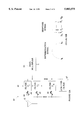
- FIG. 1 is a schematic drawing of one embodiment of a RF tag according to the present invention.
- FIG. 2 illustrates a typical interrogation signal which is a relatively broad-band signal.
- FIG. 3 illustrates a response signal that is generated by notch filtering the interrogation signal shown in FIG. 2.
- FIG. 4 is a schematic drawing of a cross-sectional view of one embodiment of an acoustical resonator according to the present invention.
- FIG. 5 is a schematic drawing of an embodiment of a RF tag according to the present invention which utilizes an acoustic resonator to process the interrogation signal received by an antenna.
- FIG. 6 illustrates a broad band interrogation signal
- FIG. 7 illustrates the output signal generated by the RF tag shown in FIG. 5.
- FIG. 8 is a block diagram of an RF tag according to the present invention having multiple FBAR resonators.
- FIG. 9 illustrates the output signal generated by the RF tag shown in FIG. 8.
- FIG. 10 is a cross-sectional view of a resonator that may be utilized to implement a bandpass filter.
- FIG. 11A is the electrical equivalent circuit of the bandpass filter shown in FIG. 10.
- FIG. 11B illustrates the transformation of an interrogation signal obtained by passing the signal through a bandpass filter of the type shown in FIG. 10.
- FIG. 12B illustrates the response of the RF tag shown in FIG. 12A to a broad-band interrogation signal.
- FIG. 13 is a cross-sectional view of two acoustical resonators constructed on a thin member having a tapered cross-section.
- FIGS. 14 and 15 are cross-sectional views of a silicon substrate at various stages of construction of a tapered member such as that shown in FIG. 13.
- FIG. 16 is a top, schematic view of the etchant flow pattern under a silicon nitride layer when pillars are utilized as baffles for slowing the flow.
- the present invention utilizes a thin film bulk acoustic resonator (FBAR) to modify the interrogation signal thereby providing a unique RF signal that identifies the tag.
- FIG. 1 is a schematic drawing of one embodiment of a RF tag according to the present invention.
- RF tag 10 receives an interrogation signal on antenna 12.
- the interrogation signal is a relatively broad-band signal extending from a low frequency of I L to a high frequency of I H as shown in FIG. 2.
- Antenna 12 is connected to a tank circuit 14 which absorbs energy at frequency F.
- the signal that is re-radiated by RF tag 10 is notch filtered as shown in FIG. 3.
- the interrogator identifies the RF tag by the position of the notch.
- the notch filter is constructed from a thin film bulk acoustic resonator (FBAR).
- FBAR 20 includes bottom and top electrodes 23 and 21, respectively, which sandwich a portion of a sheet of piezoelectric (PZ) material 22.
- PZ piezoelectric
- the preferred PZ material is aluminum nitride, AIN.
- the electrodes used in resonator 10 will be assumed to be made from aluminum; however, embodiments employing other materials may also be used.
- These devices use bulk longitudinal acoustic waves in the thin film PZ material.
- the PZ material converts some of the electrical energy into mechanical energy in the form of sound waves.
- the sound waves propagate in the same direction as the electric field and reflect off of the electrode/air interface.
- the device appears to be an electronic resonator; hence, the device can act as a notch filter.
- the mechanical resonant frequency is the frequency for which the half wavelength of the sound waves propagating in the device is equal to the total thickness of the device for a given phase velocity of sound in the material. Since the velocity of sound is many orders of magnitude smaller than the velocity of light, the resulting resonator can be quite compact.
- Resonators for applications in the GHz range may be constructed with physical dimensions less than 100 ⁇ m in diameter and few ⁇ m in thickness.
- FIG. 5 is a schematic drawing of an embodiment of a RF tag 30 according to the present invention which utilizes a resonator 31 and a frequency multiplier circuit 32 to process the interrogation signal received by an antenna 12.
- Resonator 31 is preferably an FBAR as described above.
- Frequency multiplier circuit 32 generates copies of the interrogation signal at integer multiples of the interrogation signal as shown in FIG. 6.
- Frequency multiplier 32 may be constructed from zero bias diodes, and hence, does not require a power source.
- the resonance frequency of resonator 31 is chosen to lie in one of the higher frequency images. For the purposes of the present discussion, it is assumed that resonator 31 has its resonant frequency, F, between 2I L and 2I H .
- the output signal generated by RF tag 30 is shown in FIG. 6.
- frequency multiplier 32 reduces any problems resulting from the frequency overlap between the interrogation signal and the response signal. If the RF tag is near an object which strongly reflects the interrogation signal, the reflected signal can reach the interrogator with an amplitude of the same order of magnitude as the response signal from the RF tag. This background signal can interfere with the detection of the response signal. By moving the response signal to a higher frequency, such interference is avoided.
- each radio tag has a unique identification number which can be detected by the interrogator.
- personnel ID badges can be constructed from such a set of RF tags.
- a set of RF tags could be constructed by using the embodiment shown in FIG. 5 with a different resonant frequency for each tag.
- the separation between the various frequencies becomes too small to provide reliable detection.
- each tag can be made to transmit a unique binary encoded identification signal.
- FIG. 8 is a block diagram of an RF tag 40 constructed from N FBAR resonators. Exemplary resonators are shown at 41-43. Each resonator absorbs energy at a unique frequency. The absorption frequency of the i th resonator is denoted by F i . For the purposes of this discussion, all of the resonant frequencies are assumed to be within one of the high frequency signal images generated by frequency multiplier 44.
- the output of RF tag 40 when all of the resonators are connected to antenna 12 is shown in FIG. 9.
- each of the resonators is connected to the antenna by a fuse 45 which may be blown by connecting the RF tag to an appropriate programming device.
- the lowest and highest frequency resonators are always connected.
- This arrangement provides two calibration peaks at the extremes of the frequency band in which the other peaks may be present or absent depending on the identification number. It is known that the resonant frequency of an FBAR will shift with temperature. These calibration peaks allow the interrogator to correct for any such shift. In this case, the actual identification number is limited to N-2 bits.
- FIG. 1 illustrates the equivalent circuit for an antenna connected to an FBAR.
- the antenna load, Z 0 must satisfy the condition: ##EQU1##
- the circuit parameters are related to the area of the FBAR layers.
- the device areas are chosen such that Eq(1) is satisfied.
- the device areas are chosen such that: ##EQU2##
- Bandpass filters may also be constructed from thin film bulk resonators.
- FIG. 10 is a cross-sectional view of bandpass filter 400.
- the electrically equivalent circuit is shown in FIG. 11A.
- Filter 400 is basically two FBAR filters that are mechanically coupled. A signal across electrodes 403 and 404 at the resonance frequency of PZ layer 401 will transmit acoustical energy to PZ layer 402. The mechanical oscillations in PZ layer 402 are converted to an electrical signal across electrodes 404 and 405 by the PZ material. Hence, a broadband interrogation signal such as that shown in FIG. 11B will be converted to a narrow band response signal at the resonant frequency of the resonators.
- One or more bandpass filters can be combined with an antenna and, optionally, a frequency multiplication circuit to form an RF tag which transmits an identification signal which includes a binary coded identification number.
- FIG. 12A is a block diagram of an RF tag 60 having N bandpass filters for implementing an N-2 bit identification code in a manner analogous to that described above with reference to FIGS. 8 and 9. Exemplary filters are shown at 63.
- the interrogation signal is a broadband signal occupying the frequencies between I L and I H .
- RF tag 60 utilizes bandpass filters having pass-bands between 2I L and 2I H , the center frequency of the pass-band of the i th filter being denoted by F i .
- the interrogation signal is received by antenna 12 and coupled to frequency multiplier 52 by low-pass filter 67.
- Low-pass filter 67 has an upper cut-off frequency between I H and 2I L , Frequency multiplier 52 generates images of the interrogation signal at integer multiples of the interrogation frequencies.
- the higher-order interrogation image signals are blocked from returning to antenna 12 by low-pass filter 67.
- the portion of the image between 2I L and 2I H that overlaps the pass-bands of the filters returns to antenna 12. All other images of the interrogation signal created by frequency multiplier 52 are blocked. Accordingly, a response signal such as that shown in FIG. 12B is created if all of the filters are connected to antenna 12.
- the above described embodiments of the present invention utilize the frequency of one or more resonators to provide the RF tag identification.
- the frequency is controlled primarily by controlling the thickness of the PZ layer.
- the resonance frequency can be shifted slightly by altering the area of the electrodes, and hence, the device.
- the area of the electrodes determines the phase shift introduced into the band-passed signal in bandpass embodiments of the present invention.
- the simplest method for constructing devices with different resonant frequencies is to utilize differences in the thickness of the devices.
- an FBAR or SBAR can be fabricated on a thin membrane. Since the device sits on this substrate, the device appears to be loaded with a mass that is related to the thickness of the membrane under the device. The loading of the device shifts the resonant frequency downward from the frequency that would be observed if the device was suspended in air. Accordingly, the resonant frequency of the device may be altered by changing the thickness of the membrane.
- FIG. 13 is a cross-sectional view of two FBARs 131 and 132 constructed on a thin member 133 having a tapered cross-section.
- member 133 is constructed by etching a cavity 134 in a substrate 135.
- the two FBARs are isolated from one another by a pillar 136 which extends to the bottom of the cavity.
- FIGS. 14-15 are cross-sectional views of a silicon substrate at various stages of construction of a tapered member such as that shown in FIG. 13.
- a pit is formed in a silicon substrate 140 and filled with a low temperature phospho-silica-glass (PSG).
- PSG is then planarized as shown at 141 and a layer of silicon nitride 142 is deposited and patterned over the filled pit such that an opening 143 at one end of the silicon nitride layer exposes part of the PSG.
- the substrate is then etched using a solution of HF and water as shown in FIG. 15.
- the etch rate of PSG is such that PSG is etched much faster than the silicon nitride.
- the ratio of the etch rates depends on the specific silicon nitride and PSG formulations; however, etch rate ratios of 1000:1 or greater are easily obtained.
- the portion of the silicon nitride layer nearest to opening 143 is exposed to the etchant much longer than the portions nearer to region 145. Hence, the resulting silicon nitride layer 144 will be tapered by an amount determined by the etch rate ratio.
- a pillar may be utilized to isolate the FBARs from one another on the supporting member. This can be accomplished by masking the silicon substrate so as to leave pillars in the pit shown in FIG. 13. The pillars must allow the etchant to move under the silicon nitride layer.
- the pillars can also be used to increase the etch ratio by slowing the advance of the etchant front as shown in FIG. 16 which is a top, schematic view of the etchant flow pattern under a silicon nitride layer.
- the layer which is not shown, is constructed over a pit 160 in substrate 161 having a plurality of pillars shown at 163.
- the etchant enters the pit at 164 and progressively dissolves the PSG fill 165.
- the flow of the etchant wave front is retarded by the pillars which restrict the flow of the etchant.
- This approach of selectively "thinning" the SiN creates local thickness variation, and thus a multiplicity of frequencies for use as an RF tag as shown in FIG. 8 or FIG. 12A.
- a device with its plurality of filters (or resonators) can be a template that is repeated across a wafer, yielding many RF-ID tags per silicon wafer.
- Uniqueness of ID can be accomplished by selectively connecting a unique set of filter/resonators via a fuse or other means.
- the present invention provides a method for constructing inexpensive RF ID tags.
Abstract
Description
Claims (13)
Priority Applications (1)
| Application Number | Priority Date | Filing Date | Title |
|---|---|---|---|
| US08/909,677 US5883575A (en) | 1997-08-12 | 1997-08-12 | RF-tags utilizing thin film bulk wave acoustic resonators |
Applications Claiming Priority (1)
| Application Number | Priority Date | Filing Date | Title |
|---|---|---|---|
| US08/909,677 US5883575A (en) | 1997-08-12 | 1997-08-12 | RF-tags utilizing thin film bulk wave acoustic resonators |
Publications (1)
| Publication Number | Publication Date |
|---|---|
| US5883575A true US5883575A (en) | 1999-03-16 |
Family
ID=25427648
Family Applications (1)
| Application Number | Title | Priority Date | Filing Date |
|---|---|---|---|
| US08/909,677 Expired - Lifetime US5883575A (en) | 1997-08-12 | 1997-08-12 | RF-tags utilizing thin film bulk wave acoustic resonators |
Country Status (1)
| Country | Link |
|---|---|
| US (1) | US5883575A (en) |
Cited By (38)
| Publication number | Priority date | Publication date | Assignee | Title |
|---|---|---|---|---|
| US6044353A (en) * | 1998-03-10 | 2000-03-28 | Pugliese, Iii; Anthony V. | Baggage check-in and security system and method |
| US6104119A (en) * | 1998-03-06 | 2000-08-15 | Motorola, Inc. | Piezoelectric switch |
| EP1111780A3 (en) * | 1999-12-22 | 2001-07-04 | Philips Corporate Intellectual Property GmbH | Filter |
| US6306313B1 (en) | 2000-02-04 | 2001-10-23 | Agere Systems Guardian Corp. | Selective etching of thin films |
| US6323744B1 (en) | 2000-02-04 | 2001-11-27 | Agere Systems Guardian Corp. | Grounding of TFR ladder filters |
| US6355498B1 (en) | 2000-08-11 | 2002-03-12 | Agere Systems Guartian Corp. | Thin film resonators fabricated on membranes created by front side releasing |
| US6377137B1 (en) | 2000-09-11 | 2002-04-23 | Agilent Technologies, Inc. | Acoustic resonator filter with reduced electromagnetic influence due to die substrate thickness |
| US6377136B1 (en) | 2000-02-04 | 2002-04-23 | Agere Systems Guardian Corporation | Thin film resonator filter having at least one component with different resonant frequency sets or electrode capacitance |
| US6396075B1 (en) * | 1998-05-27 | 2002-05-28 | Texas Instruments Incorporated | Transient fuse for change-induced damage detection |
| US6424237B1 (en) | 2000-12-21 | 2002-07-23 | Agilent Technologies, Inc. | Bulk acoustic resonator perimeter reflection system |
| US6437667B1 (en) | 2000-02-04 | 2002-08-20 | Agere Systems Guardian Corp. | Method of tuning thin film resonator filters by removing or adding piezoelectric material |
| US6486751B1 (en) | 2000-09-26 | 2002-11-26 | Agere Systems Inc. | Increased bandwidth thin film resonator having a columnar structure |
| US20020185936A1 (en) * | 1999-11-01 | 2002-12-12 | Barber Bradley Paul | Incremental tuning process for electrical resonators based on mechanical motion |
| US20030001726A1 (en) * | 1999-08-09 | 2003-01-02 | Micron Technology, Inc. | RFID material tracking method and apparatus |
| US6524971B1 (en) | 1999-12-17 | 2003-02-25 | Agere Systems, Inc. | Method of deposition of films |
| US6587212B1 (en) | 2000-10-31 | 2003-07-01 | Agere Systems Inc. | Method and apparatus for studying vibrational modes of an electro-acoustic device |
| US6600389B2 (en) * | 2001-05-30 | 2003-07-29 | Intel Corporation | Tapered structures for generating a set of resonators with systematic resonant frequencies |
| US6603241B1 (en) | 2000-05-23 | 2003-08-05 | Agere Systems, Inc. | Acoustic mirror materials for acoustic devices |
| US6674291B1 (en) | 2000-10-30 | 2004-01-06 | Agere Systems Guardian Corp. | Method and apparatus for determining and/or improving high power reliability in thin film resonator devices, and a thin film resonator device resultant therefrom |
| US6743731B1 (en) | 2000-11-17 | 2004-06-01 | Agere Systems Inc. | Method for making a radio frequency component and component produced thereby |
| US6746577B1 (en) | 1999-12-16 | 2004-06-08 | Agere Systems, Inc. | Method and apparatus for thickness control and reproducibility of dielectric film deposition |
| US6782750B1 (en) * | 1999-10-19 | 2004-08-31 | Terje Melandso | Device for hidden coding of an object and method for reading |
| US20040189473A1 (en) * | 2003-01-27 | 2004-09-30 | Mickle Marlin H. | RFID radio frequency identification or property monitoring method and associated apparatus |
| US20040217171A1 (en) * | 2003-04-29 | 2004-11-04 | Devos John A. | Electronic identification label and interrogator for use therewith |
| WO2005031637A1 (en) * | 2003-09-29 | 2005-04-07 | Koninklijke Philips Electronics N.V. | System, station, device and method for obtaining quantities |
| US20050137890A1 (en) * | 2003-12-22 | 2005-06-23 | Endicott Interconnect Technologies, Inc. | Item identification and control system |
| EP1126601A3 (en) * | 2000-02-04 | 2006-03-22 | Lucent Technologies Inc. | Method of isolation for acoustic resonator devices |
| US20060244436A1 (en) * | 2005-04-29 | 2006-11-02 | Trutna William R Jr | Resonator based spectrum analyzer and method |
| US20070058707A1 (en) * | 2005-09-15 | 2007-03-15 | Trutna William R Jr | Detecting wireless channel status from acoustic discrimination of spectral content |
| US20070290767A1 (en) * | 2006-06-19 | 2007-12-20 | Maxim Integrated Products, Inc. | Impedance transformation and filter using bulk acoustic wave technology |
| US20080117052A1 (en) * | 2005-05-26 | 2008-05-22 | Robert Tiernay | Intermodulation mitigation technique in an RFID system |
| US20080231410A1 (en) * | 2004-04-20 | 2008-09-25 | Frank Anthony Doljack | RFID Open Fuse Indicator, System, and Method |
| US7435613B2 (en) | 2001-02-12 | 2008-10-14 | Agere Systems Inc. | Methods of fabricating a membrane with improved mechanical integrity |
| US20090001595A1 (en) * | 2007-06-29 | 2009-01-01 | Ulrike Roessner | Integrated Circuit, Intermediate Structure and a Method of Fabricating a Semiconductor Structure |
| US20090179714A1 (en) * | 2006-06-19 | 2009-07-16 | Ali-Ahmad Walid Y | Harmonic Termination Of Power Amplifiers Using BAW Filter Output Matching Circuits |
| WO2018004669A1 (en) * | 2016-07-01 | 2018-01-04 | Intel Corporation | Techniques for monolithic co-integration of thin-film bulk acoustic resonator devices and iii-n semiconductor transistor devices |
| WO2018004668A3 (en) * | 2016-07-01 | 2018-02-22 | Intel Corporation | Techniques for forming thin-film bulk acoustic resonator devices |
| US20220123729A1 (en) * | 2019-07-31 | 2022-04-21 | QXONIX Inc. | Acoustic devices structures, filters and systems |
Citations (7)
| Publication number | Priority date | Publication date | Assignee | Title |
|---|---|---|---|---|
| US2976501A (en) * | 1959-07-30 | 1961-03-21 | Oskar E Mattiat | Impedance transformer |
| US3755803A (en) * | 1969-04-02 | 1973-08-28 | Unisearch Ltd | Electronic surveillance system |
| US5034753A (en) * | 1989-06-01 | 1991-07-23 | Weber Robert J | Acoustically coupled antenna |
| US5359250A (en) * | 1992-03-04 | 1994-10-25 | The Whitaker Corporation | Bulk wave transponder |
| US5382930A (en) * | 1992-12-21 | 1995-01-17 | Trw Inc. | Monolithic multipole filters made of thin film stacked crystal filters |
| US5446306A (en) * | 1993-12-13 | 1995-08-29 | Trw Inc. | Thin film voltage-tuned semiconductor bulk acoustic resonator (SBAR) |
| US5587620A (en) * | 1993-12-21 | 1996-12-24 | Hewlett-Packard Company | Tunable thin film acoustic resonators and method for making the same |
-
1997
- 1997-08-12 US US08/909,677 patent/US5883575A/en not_active Expired - Lifetime
Patent Citations (7)
| Publication number | Priority date | Publication date | Assignee | Title |
|---|---|---|---|---|
| US2976501A (en) * | 1959-07-30 | 1961-03-21 | Oskar E Mattiat | Impedance transformer |
| US3755803A (en) * | 1969-04-02 | 1973-08-28 | Unisearch Ltd | Electronic surveillance system |
| US5034753A (en) * | 1989-06-01 | 1991-07-23 | Weber Robert J | Acoustically coupled antenna |
| US5359250A (en) * | 1992-03-04 | 1994-10-25 | The Whitaker Corporation | Bulk wave transponder |
| US5382930A (en) * | 1992-12-21 | 1995-01-17 | Trw Inc. | Monolithic multipole filters made of thin film stacked crystal filters |
| US5446306A (en) * | 1993-12-13 | 1995-08-29 | Trw Inc. | Thin film voltage-tuned semiconductor bulk acoustic resonator (SBAR) |
| US5587620A (en) * | 1993-12-21 | 1996-12-24 | Hewlett-Packard Company | Tunable thin film acoustic resonators and method for making the same |
Cited By (75)
| Publication number | Priority date | Publication date | Assignee | Title |
|---|---|---|---|---|
| US6104119A (en) * | 1998-03-06 | 2000-08-15 | Motorola, Inc. | Piezoelectric switch |
| US6044353A (en) * | 1998-03-10 | 2000-03-28 | Pugliese, Iii; Anthony V. | Baggage check-in and security system and method |
| US6586267B2 (en) * | 1998-05-27 | 2003-07-01 | Texas Instruments Incorporated | Transient fuse for charge-induced damage detection |
| US6396075B1 (en) * | 1998-05-27 | 2002-05-28 | Texas Instruments Incorporated | Transient fuse for change-induced damage detection |
| US7808367B2 (en) * | 1999-08-09 | 2010-10-05 | Round Rock Research, Llc | RFID material tracking method and apparatus |
| US20030001726A1 (en) * | 1999-08-09 | 2003-01-02 | Micron Technology, Inc. | RFID material tracking method and apparatus |
| US6782750B1 (en) * | 1999-10-19 | 2004-08-31 | Terje Melandso | Device for hidden coding of an object and method for reading |
| US20050224450A1 (en) * | 1999-11-01 | 2005-10-13 | Lucent Technologies Inc. | Incremental tuning process for electrical resonators based on mechanical motion |
| US7631412B2 (en) | 1999-11-01 | 2009-12-15 | Agere Systems Inc. | Incremental tuning process for electrical resonators based on mechanical motion |
| US20080028584A1 (en) * | 1999-11-01 | 2008-02-07 | Agere Systems Inc. | Incremental tuning process for electrical resonators based on mechanical motion |
| US20020185936A1 (en) * | 1999-11-01 | 2002-12-12 | Barber Bradley Paul | Incremental tuning process for electrical resonators based on mechanical motion |
| US7328497B2 (en) | 1999-11-01 | 2008-02-12 | Agere Systems Inc. | Incremental tuning process for electrical resonators based on mechanical motion |
| US6746577B1 (en) | 1999-12-16 | 2004-06-08 | Agere Systems, Inc. | Method and apparatus for thickness control and reproducibility of dielectric film deposition |
| US6524971B1 (en) | 1999-12-17 | 2003-02-25 | Agere Systems, Inc. | Method of deposition of films |
| US6768396B2 (en) | 1999-12-22 | 2004-07-27 | Koninklijke Philips Electronics N.V. | Filter arrangement |
| EP1111780A3 (en) * | 1999-12-22 | 2001-07-04 | Philips Corporate Intellectual Property GmbH | Filter |
| US6377136B1 (en) | 2000-02-04 | 2002-04-23 | Agere Systems Guardian Corporation | Thin film resonator filter having at least one component with different resonant frequency sets or electrode capacitance |
| US6306313B1 (en) | 2000-02-04 | 2001-10-23 | Agere Systems Guardian Corp. | Selective etching of thin films |
| US6323744B1 (en) | 2000-02-04 | 2001-11-27 | Agere Systems Guardian Corp. | Grounding of TFR ladder filters |
| US7296329B1 (en) | 2000-02-04 | 2007-11-20 | Agere Systems Inc. | Method of isolation for acoustic resonator device |
| US6437667B1 (en) | 2000-02-04 | 2002-08-20 | Agere Systems Guardian Corp. | Method of tuning thin film resonator filters by removing or adding piezoelectric material |
| US8631547B2 (en) | 2000-02-04 | 2014-01-21 | Agere Systems Inc. | Method of isolation for acoustic resonator device |
| EP1126601A3 (en) * | 2000-02-04 | 2006-03-22 | Lucent Technologies Inc. | Method of isolation for acoustic resonator devices |
| US6603241B1 (en) | 2000-05-23 | 2003-08-05 | Agere Systems, Inc. | Acoustic mirror materials for acoustic devices |
| US6355498B1 (en) | 2000-08-11 | 2002-03-12 | Agere Systems Guartian Corp. | Thin film resonators fabricated on membranes created by front side releasing |
| US6377137B1 (en) | 2000-09-11 | 2002-04-23 | Agilent Technologies, Inc. | Acoustic resonator filter with reduced electromagnetic influence due to die substrate thickness |
| US6486751B1 (en) | 2000-09-26 | 2002-11-26 | Agere Systems Inc. | Increased bandwidth thin film resonator having a columnar structure |
| US6674291B1 (en) | 2000-10-30 | 2004-01-06 | Agere Systems Guardian Corp. | Method and apparatus for determining and/or improving high power reliability in thin film resonator devices, and a thin film resonator device resultant therefrom |
| US6675450B1 (en) | 2000-10-30 | 2004-01-13 | Agere Systems Guardian Corp. | Method of manufacturing and mounting electronic devices to limit the effects of parasitics |
| US20040163244A1 (en) * | 2000-10-30 | 2004-08-26 | Agere Systems Inc. | Method of manufacturing and mounting electronic devices to limit the effects of parasitics |
| US6587212B1 (en) | 2000-10-31 | 2003-07-01 | Agere Systems Inc. | Method and apparatus for studying vibrational modes of an electro-acoustic device |
| US20040195684A1 (en) * | 2000-11-17 | 2004-10-07 | Huggins Harold Alexis | Method for making a radio frequency component and component produced thereby |
| US6743731B1 (en) | 2000-11-17 | 2004-06-01 | Agere Systems Inc. | Method for making a radio frequency component and component produced thereby |
| US6424237B1 (en) | 2000-12-21 | 2002-07-23 | Agilent Technologies, Inc. | Bulk acoustic resonator perimeter reflection system |
| US7895720B2 (en) | 2001-02-12 | 2011-03-01 | Agere Systems Inc. | Methods of fabricating a membrane with improved mechanical integrity |
| US8225472B2 (en) | 2001-02-12 | 2012-07-24 | Agere Systems Inc. | Methods of fabricating a membrane with improved mechanical integrity |
| US7435613B2 (en) | 2001-02-12 | 2008-10-14 | Agere Systems Inc. | Methods of fabricating a membrane with improved mechanical integrity |
| US20110115338A1 (en) * | 2001-02-12 | 2011-05-19 | Agere Systems Inc. | Methods of Fabricating a Membrane With Improved Mechanical Integrity |
| US20090049670A1 (en) * | 2001-02-12 | 2009-02-26 | Agere Systems Inc. | Methods of fabricating a membrane with improved mechanical integrity |
| US6600389B2 (en) * | 2001-05-30 | 2003-07-29 | Intel Corporation | Tapered structures for generating a set of resonators with systematic resonant frequencies |
| US20040189473A1 (en) * | 2003-01-27 | 2004-09-30 | Mickle Marlin H. | RFID radio frequency identification or property monitoring method and associated apparatus |
| US7283053B2 (en) * | 2003-01-27 | 2007-10-16 | University Of Pittsburgh - Of The Commonwealth System Of Higher Education | RFID radio frequency identification or property monitoring method and associated apparatus |
| US7014112B2 (en) | 2003-04-29 | 2006-03-21 | Hewlett-Packard Development Company, L.P. | Electronic identification label and interrogator for use therewith |
| US20040217171A1 (en) * | 2003-04-29 | 2004-11-04 | Devos John A. | Electronic identification label and interrogator for use therewith |
| US20070064774A1 (en) * | 2003-09-29 | 2007-03-22 | Koninklijke Philips Electronics N.V. | System, station, device and method for obtaining quantities |
| WO2005031637A1 (en) * | 2003-09-29 | 2005-04-07 | Koninklijke Philips Electronics N.V. | System, station, device and method for obtaining quantities |
| US20050137890A1 (en) * | 2003-12-22 | 2005-06-23 | Endicott Interconnect Technologies, Inc. | Item identification and control system |
| US7801833B2 (en) | 2003-12-22 | 2010-09-21 | Endicott Interconnect Technologies, Inc. | Item identification control method |
| US8134445B2 (en) * | 2004-04-20 | 2012-03-13 | Cooper Technologies Company | RFID open fuse indicator, system, and method |
| US20080231410A1 (en) * | 2004-04-20 | 2008-09-25 | Frank Anthony Doljack | RFID Open Fuse Indicator, System, and Method |
| US7276892B2 (en) * | 2005-04-29 | 2007-10-02 | Avago Technologies Wireless Ip (Singapore) Pte. Ltd. | Resonator based spectrum analyzer and method |
| US20060244436A1 (en) * | 2005-04-29 | 2006-11-02 | Trutna William R Jr | Resonator based spectrum analyzer and method |
| US20140347167A1 (en) * | 2005-05-26 | 2014-11-27 | Amtech Systems, LLC | Intermodulation mitigation technique in an rfid system |
| US8237565B2 (en) | 2005-05-26 | 2012-08-07 | Amtech Systems, LLC | Intermodulation mitigation technique in an RFID system |
| US8810403B2 (en) * | 2005-05-26 | 2014-08-19 | Amtech Systems, LLC | Intermodulation mitigation technique in an RFID system |
| US7772977B2 (en) | 2005-05-26 | 2010-08-10 | Tc License Ltd. | Intermodulation mitigation technique in an RFID system |
| US20130119132A1 (en) * | 2005-05-26 | 2013-05-16 | Robert Tiernay | Intermodulation mitigation technique in an rfid system |
| US7518532B2 (en) * | 2005-05-26 | 2009-04-14 | Tc License Ltd. | Intermodulation mitigation technique in an RFID system |
| US20090206998A1 (en) * | 2005-05-26 | 2009-08-20 | Robert Tiernay | Intermodulation mitigation technique in an rfid system |
| US20110025470A1 (en) * | 2005-05-26 | 2011-02-03 | Robert Tiernay | Automatic mode detection in a dual mode rfid tag |
| US20080117052A1 (en) * | 2005-05-26 | 2008-05-22 | Robert Tiernay | Intermodulation mitigation technique in an RFID system |
| US9558383B2 (en) * | 2005-05-26 | 2017-01-31 | Amtech Systems, LLC | Intermodulation mitigation technique in an RFID system |
| US20070058707A1 (en) * | 2005-09-15 | 2007-03-15 | Trutna William R Jr | Detecting wireless channel status from acoustic discrimination of spectral content |
| US8094704B2 (en) | 2005-09-15 | 2012-01-10 | Avago Technologies Wiresless IP (Singapore) Pte. Ltd. | Detecting wireless channel status from acoustic discrimination of spectral content |
| US7728696B2 (en) | 2006-06-19 | 2010-06-01 | Maxim Integrated Products, Inc. | Harmonic termination of power amplifiers using BAW filter output matching circuits |
| US20070290767A1 (en) * | 2006-06-19 | 2007-12-20 | Maxim Integrated Products, Inc. | Impedance transformation and filter using bulk acoustic wave technology |
| US7586389B2 (en) | 2006-06-19 | 2009-09-08 | Maxim Integrated Products, Inc. | Impedance transformation and filter using bulk acoustic wave technology |
| US20090179714A1 (en) * | 2006-06-19 | 2009-07-16 | Ali-Ahmad Walid Y | Harmonic Termination Of Power Amplifiers Using BAW Filter Output Matching Circuits |
| US7598827B2 (en) | 2006-06-19 | 2009-10-06 | Maxim Integrated Products | Harmonic termination of power amplifiers using BAW filter output matching circuits |
| US7858514B2 (en) * | 2007-06-29 | 2010-12-28 | Qimonda Ag | Integrated circuit, intermediate structure and a method of fabricating a semiconductor structure |
| US20090001595A1 (en) * | 2007-06-29 | 2009-01-01 | Ulrike Roessner | Integrated Circuit, Intermediate Structure and a Method of Fabricating a Semiconductor Structure |
| WO2018004669A1 (en) * | 2016-07-01 | 2018-01-04 | Intel Corporation | Techniques for monolithic co-integration of thin-film bulk acoustic resonator devices and iii-n semiconductor transistor devices |
| WO2018004668A3 (en) * | 2016-07-01 | 2018-02-22 | Intel Corporation | Techniques for forming thin-film bulk acoustic resonator devices |
| US11043627B2 (en) | 2016-07-01 | 2021-06-22 | Intel Corporation | Techniques for monolithic co-integration of thin-film bulk acoustic resonator devices and III-N semiconductor transistor devices |
| US20220123729A1 (en) * | 2019-07-31 | 2022-04-21 | QXONIX Inc. | Acoustic devices structures, filters and systems |
Similar Documents
| Publication | Publication Date | Title |
|---|---|---|
| US5883575A (en) | RF-tags utilizing thin film bulk wave acoustic resonators | |
| US7095298B2 (en) | Film bulk acoustic resonator having supports and manufacturing method therefore | |
| US5446447A (en) | RF tagging system including RF tags with variable frequency resonant circuits | |
| US10361677B2 (en) | Transverse bulk acoustic wave filter | |
| EP1538747B1 (en) | Micromechanical electrostatic resonator | |
| US7005946B2 (en) | MEMS piezoelectric longitudinal mode resonator | |
| US4951057A (en) | Inductive input/output coupling for a surface acoustic wave device | |
| EP1469599B1 (en) | Air gap type FBAR, duplexer using the FBAR, and fabricating methods thereof | |
| KR100316383B1 (en) | Structure and Fabrication of Single-chip Radio Integrating Thin or Thick Film Piezoelectric Crystal Devices on Monolithic Integrated Circuits | |
| US6295247B1 (en) | Micromachined rayleigh, lamb, and bulk wave capacitive ultrasonic transducers | |
| US6601276B2 (en) | Method for self alignment of patterned layers in thin film acoustic devices | |
| US5552655A (en) | Low frequency mechanical resonator | |
| AU740252B2 (en) | Circuit chip mounted card and circuit chip module | |
| KR20030007587A (en) | Radio Frequency Detection and Identification System | |
| US20080252401A1 (en) | Evanescent Mode Resonator Including Tunable Capacitive Post | |
| JP2002094328A (en) | Communication signal mixing/filtering device and its manufacturing method | |
| US5359250A (en) | Bulk wave transponder | |
| CN100407227C (en) | Security element for radio frequency identification | |
| CN100511990C (en) | Piezoelectric resonator and electronic component provided therewith | |
| US7119638B2 (en) | Film bulk acoustic resonator having an air gap and a method for manufacturing the same | |
| KR100555762B1 (en) | Air-gap type ???? fabrication method and FBAR fabricated by the same, filter and duPlexer using the FBAR. | |
| US4028648A (en) | Tunable surface wave device resonator | |
| US6369374B1 (en) | Filter including a micro-mechanical resonator | |
| JP4940558B2 (en) | Wireless response device and wireless response communication system | |
| KR100616655B1 (en) | Method for forming idt electrode pattern of saw device using anti-fuse and saw device manufactured thereby |
Legal Events
| Date | Code | Title | Description |
|---|---|---|---|
| AS | Assignment |
Owner name: HEWLETT-PACKARD COMPANY, CALIFORNIA Free format text: ASSIGNMENT OF ASSIGNORS INTEREST;ASSIGNORS:RUBY, RICHARD C.;CANFIELD, PHILIP C.;REEL/FRAME:008741/0932;SIGNING DATES FROM 19970728 TO 19970813 |
|
| STCF | Information on status: patent grant |
Free format text: PATENTED CASE |
|
| AS | Assignment |
Owner name: HEWLETT-PACKARD COMPANY, A DELAWARE CORPORATION, C Free format text: MERGER;ASSIGNOR:HEWLETT-PACKARD COMPANY, A CALIFORNIA CORPORATION;REEL/FRAME:010841/0649 Effective date: 19980520 |
|
| AS | Assignment |
Owner name: AGILENT TECHNOLOGIES INC, CALIFORNIA Free format text: ASSIGNMENT OF ASSIGNORS INTEREST;ASSIGNOR:HEWLETT-PACKARD COMPANY;REEL/FRAME:010977/0540 Effective date: 19991101 |
|
| FEPP | Fee payment procedure |
Free format text: PAYOR NUMBER ASSIGNED (ORIGINAL EVENT CODE: ASPN); ENTITY STATUS OF PATENT OWNER: LARGE ENTITY |
|
| FPAY | Fee payment |
Year of fee payment: 4 |
|
| REMI | Maintenance fee reminder mailed | ||
| AS | Assignment |
Owner name: AVAGO TECHNOLOGIES GENERAL IP PTE. LTD., SINGAPORE Free format text: ASSIGNMENT OF ASSIGNORS INTEREST;ASSIGNOR:AGILENT TECHNOLOGIES, INC.;REEL/FRAME:017207/0020 Effective date: 20051201 |
|
| AS | Assignment |
Owner name: CITICORP NORTH AMERICA, INC.,DELAWARE Free format text: SECURITY AGREEMENT;ASSIGNOR:AVAGO TECHNOLOGIES GENERAL IP (SINGAPORE) PTE. LTD.;REEL/FRAME:017207/0882 Effective date: 20051201 Owner name: CITICORP NORTH AMERICA, INC., DELAWARE Free format text: SECURITY AGREEMENT;ASSIGNOR:AVAGO TECHNOLOGIES GENERAL IP (SINGAPORE) PTE. LTD.;REEL/FRAME:017207/0882 Effective date: 20051201 |
|
| AS | Assignment |
Owner name: AVAGO TECHNOLOGIES WIRELESS IP (SINGAPORE) PTE. LT Free format text: ASSIGNMENT OF ASSIGNORS INTEREST;ASSIGNOR:AVAGO TECHNOLOGIES GENERAL IP (SINGAPORE) PTE. LTD;REEL/FRAME:017675/0434 Effective date: 20060127 |
|
| FPAY | Fee payment |
Year of fee payment: 8 |
|
| FPAY | Fee payment |
Year of fee payment: 12 |
|
| AS | Assignment |
Owner name: AVAGO TECHNOLOGIES GENERAL IP (SINGAPORE) PTE. LTD Free format text: MERGER;ASSIGNOR:AVAGO TECHNOLOGIES WIRELESS IP (SINGAPORE) PTE. LTD.;REEL/FRAME:030369/0703 Effective date: 20121030 |
|
| AS | Assignment |
Owner name: AVAGO TECHNOLOGIES GENERAL IP (SINGAPORE) PTE. LTD Free format text: RELEASE BY SECURED PARTY;ASSIGNOR:CITICORP NORTH AMERICA, INC.;REEL/FRAME:030422/0001 Effective date: 20110331 |
|
| AS | Assignment |
Owner name: DEUTSCHE BANK AG NEW YORK BRANCH, AS COLLATERAL AGENT, NEW YORK Free format text: PATENT SECURITY AGREEMENT;ASSIGNOR:AVAGO TECHNOLOGIES GENERAL IP (SINGAPORE) PTE. LTD.;REEL/FRAME:032851/0001 Effective date: 20140506 Owner name: DEUTSCHE BANK AG NEW YORK BRANCH, AS COLLATERAL AG Free format text: PATENT SECURITY AGREEMENT;ASSIGNOR:AVAGO TECHNOLOGIES GENERAL IP (SINGAPORE) PTE. LTD.;REEL/FRAME:032851/0001 Effective date: 20140506 |
|
| AS | Assignment |
Owner name: AVAGO TECHNOLOGIES GENERAL IP (SINGAPORE) PTE. LTD., SINGAPORE Free format text: TERMINATION AND RELEASE OF SECURITY INTEREST IN PATENT RIGHTS (RELEASES RF 032851-0001);ASSIGNOR:DEUTSCHE BANK AG NEW YORK BRANCH, AS COLLATERAL AGENT;REEL/FRAME:037689/0001 Effective date: 20160201 Owner name: AVAGO TECHNOLOGIES GENERAL IP (SINGAPORE) PTE. LTD Free format text: TERMINATION AND RELEASE OF SECURITY INTEREST IN PATENT RIGHTS (RELEASES RF 032851-0001);ASSIGNOR:DEUTSCHE BANK AG NEW YORK BRANCH, AS COLLATERAL AGENT;REEL/FRAME:037689/0001 Effective date: 20160201 |
|
| AS | Assignment |
Owner name: BANK OF AMERICA, N.A., AS COLLATERAL AGENT, NORTH CAROLINA Free format text: PATENT SECURITY AGREEMENT;ASSIGNOR:AVAGO TECHNOLOGIES GENERAL IP (SINGAPORE) PTE. LTD.;REEL/FRAME:037808/0001 Effective date: 20160201 Owner name: BANK OF AMERICA, N.A., AS COLLATERAL AGENT, NORTH Free format text: PATENT SECURITY AGREEMENT;ASSIGNOR:AVAGO TECHNOLOGIES GENERAL IP (SINGAPORE) PTE. LTD.;REEL/FRAME:037808/0001 Effective date: 20160201 |
|
| AS | Assignment |
Owner name: AVAGO TECHNOLOGIES GENERAL IP (SINGAPORE) PTE. LTD Free format text: CORRECTIVE ASSIGNMENT TO CORRECT THE NAME OF THE ASSIGNEE PREVIOUSLY RECORDED ON REEL 017207 FRAME 0020. ASSIGNOR(S) HEREBY CONFIRMS THE ASSIGNMENT;ASSIGNOR:AGILENT TECHNOLOGIES, INC.;REEL/FRAME:038633/0001 Effective date: 20051201 |
|
| AS | Assignment |
Owner name: AVAGO TECHNOLOGIES GENERAL IP (SINGAPORE) PTE. LTD., SINGAPORE Free format text: TERMINATION AND RELEASE OF SECURITY INTEREST IN PATENTS;ASSIGNOR:BANK OF AMERICA, N.A., AS COLLATERAL AGENT;REEL/FRAME:041710/0001 Effective date: 20170119 Owner name: AVAGO TECHNOLOGIES GENERAL IP (SINGAPORE) PTE. LTD Free format text: TERMINATION AND RELEASE OF SECURITY INTEREST IN PATENTS;ASSIGNOR:BANK OF AMERICA, N.A., AS COLLATERAL AGENT;REEL/FRAME:041710/0001 Effective date: 20170119 |