US5872717A - Apparatus and method for verifying the timing performance of critical paths within a circuit using a static timing analyzer and a dynamic timing analyzer - Google Patents
Apparatus and method for verifying the timing performance of critical paths within a circuit using a static timing analyzer and a dynamic timing analyzer Download PDFInfo
- Publication number
- US5872717A US5872717A US08/705,398 US70539896A US5872717A US 5872717 A US5872717 A US 5872717A US 70539896 A US70539896 A US 70539896A US 5872717 A US5872717 A US 5872717A
- Authority
- US
- United States
- Prior art keywords
- timing
- circuit
- critical
- results
- path
- Prior art date
- Legal status (The legal status is an assumption and is not a legal conclusion. Google has not performed a legal analysis and makes no representation as to the accuracy of the status listed.)
- Expired - Lifetime
Links
Images


Classifications
-
- G—PHYSICS
- G06—COMPUTING; CALCULATING OR COUNTING
- G06F—ELECTRIC DIGITAL DATA PROCESSING
- G06F30/00—Computer-aided design [CAD]
- G06F30/30—Circuit design
- G06F30/32—Circuit design at the digital level
- G06F30/33—Design verification, e.g. functional simulation or model checking
- G06F30/3315—Design verification, e.g. functional simulation or model checking using static timing analysis [STA]
-
- G—PHYSICS
- G06—COMPUTING; CALCULATING OR COUNTING
- G06F—ELECTRIC DIGITAL DATA PROCESSING
- G06F30/00—Computer-aided design [CAD]
- G06F30/30—Circuit design
- G06F30/32—Circuit design at the digital level
- G06F30/33—Design verification, e.g. functional simulation or model checking
- G06F30/3308—Design verification, e.g. functional simulation or model checking using simulation
- G06F30/3312—Timing analysis
-
- G—PHYSICS
- G06—COMPUTING; CALCULATING OR COUNTING
- G06F—ELECTRIC DIGITAL DATA PROCESSING
- G06F30/00—Computer-aided design [CAD]
- G06F30/30—Circuit design
- G06F30/32—Circuit design at the digital level
- G06F30/327—Logic synthesis; Behaviour synthesis, e.g. mapping logic, HDL to netlist, high-level language to RTL or netlist
-
- G—PHYSICS
- G06—COMPUTING; CALCULATING OR COUNTING
- G06F—ELECTRIC DIGITAL DATA PROCESSING
- G06F2119/00—Details relating to the type or aim of the analysis or the optimisation
- G06F2119/12—Timing analysis or timing optimisation
Definitions
- This invention relates generally to the design of integrated circuits. More particularly, this invention relates to a technique for verifying and improving the timing performance of critical paths within an integrated circuit by relying upon redundant timing analyses of the critical paths.
- VLSI circuits are designed using a variety of Computer Aided Design (CAD) tools.
- CAD Computer Aided Design
- EDA Electronic Design Automation
- a VLSI circuit can be characterized by a netlist.
- a netlist is a list of circuit components and interconnections between the circuit components.
- An EDA tool known as a static timing analyzer is used to verify that the circuit described in the netlist meets timing requirements.
- a static timing analyzer accesses circuit timing performance by relying upon timing attributes, as specified in a library of timing models, for individual circuit components in the netlist.
- the library of timing models includes timing information for each circuit component in the netlist.
- the timing information includes such information as the input pin capacitance, input-to-output delay, and output drive strengths. Combining this library along with a design netlist, a static timing analyzer generates critical path timing information statically without knowledge of the design's logical functionality.
- timing estimates associated with a static timing analyzer are not as accurate as those provided by a circuit simulator.
- Circuit simulators such as SPICE or HSPICE can be considered dynamic timing analyzers, although they are used for more than timing analyses. Since a circuit simulator simulates the actual operation of a circuit at the transistor level, it is relatively time consuming to obtain results from a circuit simulator, compared to a static timing analyzer that does not simulate the operation of the component, but uses static timing information for the component.
- the method of the invention includes the step of producing a first set of timing results from a static timing analyzer operating on a netlist that characterizes a circuit.
- a critical timing path within the circuit is then identified from the first set of timing results.
- the critical timing path is then converted into an equivalent schematic circuit representation.
- a simulation of the equivalent schematic circuit representation on a circuit simulator produces a second set of timing results. Timing discrepancies are then located between the first set of timing results and the second set of timing results. Based upon the timing discrepancies, cells may be substituted into the critical timing path to improve the timing performance of the critical timing path.
- the use of a circuit simulator improves upon the timing information that is provided by the static timing analyzer.
- the invention efficiently utilizes the circuit simulator through a conversion of the critical timing path into an equivalent schematic circuit representation.
- the novel conversion process includes the use of ideal circuit elements to reduce the time required for circuit simulation.
- the conversion process features correct input sensitization, in accordance with a predetermined rule set, for unconnected input nodes in the equivalent schematic circuit representation in order for the circuit simulator to simulate the same signal transitions as those estimated by the static timing analyzer.
- the sensitization is preferably applied to all combinatorial gates, multiplexers, and register elements.
- FIG. 1 illustrates an apparatus constructed in accordance with an embodiment of the invention.
- FIG. 2 illustrates processing steps, and corresponding apparatus for performing the processing steps, in accordance with an embodiment of the invention.
- FIGS. 3(a)-3(c) illustrate an equivalent circuit schematic of a critical timing path, as constructed in accordance with an embodiment of the invention.
- FIG. 4 illustrates an ideal circuit element constructed in accordance with an embodiment of the invention.
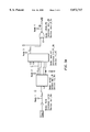
- FIG. 1 illustrates an apparatus 20 constructed in accordance with an embodiment of the invention.
- the apparatus 20 includes a Central Processing Unit (CPU) 22 that communicates with a set of input/output devices 24 over a system bus 26. Further, the CPU 22 communicates with a memory 28 via system bus 26.
- CPU Central Processing Unit
- the interaction between a CPU 22, input/output devices 24, a system bus 26, and memory 28 are known in the art.
- the present invention is directed toward the data and programs that are stored in the memory 28 and are processed by the CPU 22.
- the memory 28 stores a netlist 30, which is processed by a static timing analyzer 32.
- the static timing analyzer 32 may be implemented as the PEARLTM Timing Analyzer sold by CADENCE DESIGN AUTOMATION, Inc., San Jose, Calif.
- the static timing analyzer 32 generates a set of timing results, illustrated in FIG. 1 as a first set of timing results 34. In accordance with the prior art, this initial set of timing results is relied upon to verify that the circuit characterized by the netlist 30 meets selected timing constraints.
- the static timing analyzer 32 will identify different data paths through the circuit specified by the netlist. The data paths with the largest delays are identified by the static timing analyzer 32 as critical timing paths.
- One way to improve the timing performance of a critical timing path is to substitute relatively slow circuit components in the critical timing path with logically equivalent circuit components that are relatively fast.
- the present invention improves upon this process by obtaining more accurate timing information about a critical timing path.
- the present invention uses a circuit simulator to simulate the operation of the critical timing path. In order to achieve this benefit, a number of operations must be performed.
- FIG. 1 illustrates that the memory includes a schematic circuit constructor 36.
- the schematic circuit constructor is used to construct a schematic circuit for a critical timing path.
- the schematic circuit can then be simulated by a circuit simulator 46.
- the schematic circuit constructor 36 includes a cell matching routine 38.
- the cell matching routine 38 identifies the different cells in the critical timing path and matches each one with a corresponding schematic circuit from the schematic library 44.
- the floating node connection routine 40 establishes node connections for circuit elements in the critical timing path that include nodes that are not part of the critical timing path. In other words, the floating node connection routine 40 ties floating inputs to predetermined values so that the corresponding circuit element can be simulated accurately.
- the schematic circuit constructor 36 includes an ideal element constructor 42.
- the ideal element constructor 42 is used to establish an ideal element or circuit schematic for circuit elements that are so large that their simulation would result in an unjustified performance penalty.
- the schematic library 44 includes a set of schematic circuits for circuit elements of predetermined sizes. If a circuit element, for instance a large Arithmetic Logic Unit, exceeds that predetermined size, then the circuit element is not included in the schematic library 44. If the schematic circuit constructor 36 does not identify a match in the schematic library 44, then it constructs a corresponding ideal circuit element, as will be described below.
- the schematic circuit is simulated with a circuit simulator 46.
- the circuit simulator 46 generates a second set of timing results 48. Comparisons between the first set of timing results 34 and the second set of timing results 48 are then analyzed with a timing discrepancy analyzer 50. The discrepancies identified by this executable code are then used to provide a more accurate characterization of the timing performance of the critical timing path and the individual elements within the critical timing path. Based upon this refined information, a cell substituter 52 may be used to substitute poorly performing circuit elements in the critical timing path for logically equivalent, but faster circuit elements.
- FIG. 2 illustrates the processing steps associated with an embodiment of the invention
- FIGS. 3-4 illustrate circuit elements used to demonstrate an embodiment of the invention.
- the first processing step shown in the figure is to produce a first set of timing results (step 60). As shown on the right-hand side of the figure, this operation is performed by a static timing analyzer 32 of the type known in the art.
- the next processing step is to identify critical timing paths within the netlist (step 62). This operation is also performed with a standard static timing analyzer 32.
- the static timing analyzer 32 may report the critical timing paths in the form of a report.
- the following table is a report from a static timing analyzer for one critical timing path in a netlist.
- Table I Each row in Table I provides the following information. First, a delay value in nano-seconds is provided. Then, a node name to an instance of a circuit element is provided. Finally, the device name for the instance is provided.
- the first row of Table I lists a delay of 0.12 nano-seconds for the device or circuit element "buf -- 13x". This circuit element is a buffer available in a cell library. This circuit element may be used many times in a netlist, each "instance" of its use is assigned a different name, in this example the name is "cnln2". The input to the device is node "llclk", as shown in row 1.
- the next processing step of FIG. 2 is to convert the critical timing path into an equivalent circuit schematic (step 64).
- This operation is performed by the schematic circuit constructor 36.
- the schematic circuit constructor 36 is a set of executable instructions that identify each device in the critical timing path and then find an equivalent circuit schematic for the element in the schematic library 44.
- the first row of Table I specifies the buffer "buf -- 13x”.
- the schematic library 44 includes a netlist characterizing that buffer.
- the schematic circuit constructor 36 uses that netlist to form the first element of a schematic circuit representation of the critical path.
- the schematic circuit constructor 36 repeats this process for each element in the critical path timing report.
- FIGS. 3(a)-3(c) illustrates the schematic circuit constructed by the schematic circuit constructor 36 for the critical timing path specified in Table I. Note that each device that is specified in Table I has a schematic analog in FIGS. 3(a)-3(c).
- a floating node connection routine 40 is used to establish proper sensitization for these nodes so that the element's operation may be simulated accurately.
- the floating node connection routine relies upon a predetermined rule set and default values that are used to define connections for circuit element nodes that are not on the critical path.
- the schematic library 44 does not include schematics for relatively large devices. Such devices will substantially increase the processing time required to simulate the timing path. Thus, in accordance with the invention, such devices are preferably omitted from the schematic library 44. Instead, an ideal element constructor is used to characterize the omitted element.
- Element 80 in FIG. 3(b) is a device "sf -- m -- lbd64", which is a 64-bit leading bit detector. This relatively large element is characterized as an ideal element. That is, static timing information regarding the element is used to construct a schematic representation of the element that accurately reflects the timing properties of the element.
- the following code is an example of the data that a static timing analyzer would include for the device "sf -- m --lbd 64".
- Line (1) of the code specifies the device "sf -- m -- lbd64".
- the second line of code specifies that the device has 64 inputs "man 63:0! and that the capacitance of each input is "0.0860301" picoFarads.
- the third line of code specifies a 6-bit output bus with a corresponding output drive.
- Line (7) defines the output drive values as being "146.548" Ohms for a high output signal and "142.288" Ohms for a low output signal. Similar information is provided in lines (4) and (8).
- Line (5) specifies the inverted signal delay for the element.
- the value “0.76875” specifies a minimum low-to-high delay in nano-seconds, while the value “1.09” specifies a maximum low-to-high delay in nano-seconds.
- the value “0.76875” specifies a minimum high-to-low delay in nano-seconds, while the value “1.09” specifies a maximum high-to-low delay in nano-seconds.
- Line (8) describes similar values for a non-inverting signal.
- the foregoing information is used by a static timing analyzer 32 in a known manner to calculate a timing delay for the element "sf -- m -- lbd64" under various conditions.
- the ideal element constructor 42 fetches this information and uses it in constructing a schematic representation of the element.
- the schematic representation of the element provides accurate timing information that can be used by a circuit simulator along with the other elements in the critical timing path.
- FIG. 4 illustrates an ideal element 80 constructed in accordance with an embodiment of the invention.
- Each ideal element that is constructed may use the same schematic representation, but with different values that characterize the timing performance of the modeled element.
- the circuit schematic of FIG. 4 is described with a set of instructions. For example, the following set of instructions follow the syntax of the circuit simulator HSPICE.
- Line (10) defines a "delay” element with an "out” node and an "in” node.
- Line (11) establishes that the input capacitor “Cin”, shown in FIG. 4, has a value of 10 Farads.
- Line (12) defines the "Rout” resistor of FIG. 4 as having a value of 1 kilo-Ohm.
- Line (13) defines an ideal delay of 1 nano-second.
- the values in lines (11)-(13) are default values, substitute values are preferably passed to the code dependent upon the circuit element that is being modeled. In other words, the static timing information described in lines (1)-(8) above is used to establish values for "Cin", "rout", and "ideal -- delay". The "Cin" value is obtained from line (2) of the code.
- the "rout” value is obtained from line (7) or (8) of the code. In other words, dependent upon the operation to be performed by the circuit element, one of the values from line (7) or (8) is selected as the "rout” value. Similarly, the "ideal -- delay” value is obtained from line (5) or (6) of the code, dependent upon the operation to be performed by the circuit element.
- the ideal element constructor 42 includes a rule set for selecting these values from the static timing analyzer cell information.
- Line (14) defines an ohm value for the "rtrig” resistor shown in FIG. 4.
- line (15) defines an ohm value for the "rdelay” resistor shown in FIG. 4.
- Line (16) defines a voltage value that is used in subsequent code.
- Line (17) defines that an input capacitance "Cin” exists between the node “in” and ground ("0").
- Line (18) defines the current source “gtrig” shown in FIG. 4, which is connected between node “1” (shown in FIG. 4) and ground ("0").
- Line (18) also specifies a voltage controlled current source (VCCS) piece-wise linear (PWL) first order model.
- the control voltage is the voltage across the capacitor "Cin”, as defined with the instruction "in 0", meaning the element between the node "in” and "0".
- a scale factor of "1/rtrig" is also defined in line (18).
- Lines (19)-(22) define various output voltage values for different input voltage values.
- line (19) stipulates that if the input voltage is 0 volts, then the output voltage is set to a very low value "vlow”, which is defined as a global value.
- Line (21) states that if the input voltage is at a voltage midpoint level (say, Vdd/2), plus the previously defined “vdelta” value, then the output voltage is set to a very high value "vhigh”, which is also a global value.
- Line 23 defines the resistor "rtrig" between node 1 and ground (“0"), which is consistent with FIG. 4.
- lines (18)-(23) are used to generate a large gain around the voltage mid-point of the circuit.
- the large voltage change results in a large current across "gtrig”, which results in a large voltage across "Rtrig”.
- the voltage across "Rtrig” is used to control the voltage controlled current source “gdelay".
- the current source "gdelay” generates a current a certain time after it sees the voltage across "rtrig". That delay value is defined by the "ideal -- delay” variable, which is preferably obtained from the static timing information for this cell, as provided by lines (5) and (6) above.
- Line (24) defines the current source "gdelay” between the node "2" and ground ("0").
- the line also stipulates that the control voltage is the voltage across the element connected between node “1" and ground, which is the element "Rtrig”.
- the line defines the time delay "TD” as being equivalent to the previously discussed “ideal -- delay”.
- the same line defines a scale factor.
- Line (25) defines the "rdelay” resistor as being connected between node "2" and ground.
- Line (26) defines a voltage controlled voltage source "eout”, which is connected between node "3" and ground. The line also specifies that the control voltage is defined between node “2" and ground, which is equivalent to specifying the resistor "rdelay”. Line (27) states that the resistor "rout” is positioned between node "3" and the output node “out”.
- step 66 produces a set of timing results.
- the schematic circuit constructor 36 matches cells in the schematic library 44, connects floating nodes, and generates ideal elements, a schematic representation of the critical timing path exists. This critical timing path is then simulated by a circuit simulator to produce a set of timing results.
- An example set of timing results for the critical timing path discussed herein is shown in Table II.
- Each row of Table II defines timing information for a given node.
- Each node shown in Table II has a corresponding node shown in FIGS. 3(a)-3(b).
- the delay calculated by the static timing analyzer for that node is given in the column marked (S -- del).
- the delay calculated by the circuit simulator for a node is given in the column marked (D -- del).
- An error value is then specified in the final column. In this example, the error is defined through the following calculation:
- Timing error may be considered a step in locating timing discrepancies between the timing results, which is shown as step 68 in FIG. 2.
- a timing discrepancy analyzer 50 may be used to make these calculations and to flag large errors as candidates for cell substitution.
- the final processing step shown in FIG. 2 is to substitute cells in the critical timing path (step 70). This operation is performed with a cell substituter 52.
- the cell substituter 52 is a set of executable instructions that select a candidate cell for substitution, identifies logically equivalent cells in a cell library, and selects a logically equivalent cell that has improved timing performance.
- the use of a circuit simulator improves upon the timing accuracy that is provided by the static timing analyzer.
- the invention efficiently utilizes the circuit simulator through a novel conversion of the critical timing path into an equivalent schematic circuit representation.
- the conversion process includes the use of ideal circuit elements to reduce the time required for the dynamic timing analysis.
- the conversion process features a node connection operation to establish node connections, in accordance with a predetermined rule set, for unconnected nodes in the equivalent schematic circuit representation.
Abstract
Description
              TABLE I
______________________________________
STATIC TIMING ANALYZER CRITICAL PATH OUTPUT REPORT
Delay    Node        Instance    Device
______________________________________
0.12 ns  1lc1k       cnln2       buf.sub.-- 13x
0.12 ns  cnln2       buf.sub.-- i.sub.-- 16.sub.-- 3
                                 fs.sub.-- 16n
0.12 ns  sed.sub.-- cn1
                     cn1.sub.-- ff.sub.-- 36
                                 fs.sub.-- 8x
0.38 ns  I1930.sub.-- P8
                     xnor.sub.-- 36
                                 xnor2.sub.-- 3x
0.71 ns  lbd.sub.-- man 36!
                     sed.sub.-- lbd
                                 sf.sub.-- m.sub.-- lbd64
2.18 ns  norm.sub.-- n1 3!
                     upper.sub.-- i17
                                 not.sub.-- 12x
2.30 ns  hdr.sub.-- I.sub.-- 32
                     upper.sub.-- i18
                                 not.sub.-- 24x
2.45 ns  355.sub.-- P5
                     upper.sub.-- i10
                                 nand3.sub.-- 12x
2.73 ns  I.sub.-- 94.sub.-- P2
                     upper.sub.-- i11
                                 mnot.sub.-- 38x
2.97 ns  shift 6!.sub.-- sel2
                     byte.sub.-- shift 3!
                                 fmx8pl.sub.-- 8x
3.35 ns  I38.sub.-- p27
                     bit.sub.-- shift 10!
                                 fmx8pl.sub.-- 8x
3.62 ns  mux.sub.-- 10.sub.-- in3
                     n1.sub.-- mux.sub.-- 10
                                 mx51.sub.-- 8x
______________________________________
__________________________________________________________________________
(1)
   MODEL sf.sub.-- m.sub.-- lbd64
(2)
   INPUT "man 63:0!"
                   CAP=0.0860301
(3)
   OUTPUT "num.sub.-- ones 5:0!" DRVR=sf.sub.-- m.sub.-- lbd64.sub.--
   numones.sub.-- WCCOM
(4)
   OUTPUT "eq1.sub.-- l" DRVR=sf.sub.-- m.sub.-- lbd64.sub.-- eq1.sub.--
   WCCOM
(5)
   DELAY I "man 63:0!" *> "eq1.sub.-- l"
                         0.76875 1.09 0.76875 1.09
(6)
   DELAY E "man 63:0!"*> "num.sub.-- ones 5:0!"
                       0.58125 1.40 0.58125 1.40
(7)
   DEFDRIVER sf.sub.-- m.sub.-- lbd64.sub.-- numones.sub.-- WCCOM
                          RH=146.548 RL=142.288
(8)
   DEFDRIVER sf.sub.-- m.sub.-- lbd64.sub.-- eq1.sub.-- WCCOM
                         RH=282.306 RL=269.471
__________________________________________________________________________
______________________________________
(10)      .subckt delay out in
(11)      +cin=10F
(12)      + rout=1K
(13)      +ideal.sub.-- delay=1ns
(14)      .param rtrig = 1K
(15)      .param rdelay = 1K
(16)      .param vdelta = 0.1v
(17)      cin in 0 `cin`
(18)      gtrig 1 0 VCCS PWL(1) in 0 SCALE=`1/rtrig`
(19)      +       0v,            vlow,
(20)      +       `vmidpoint-vdelta`,
                                 vlow,
(21)      +       `vmidpoint+vdelta`,
                                 vhigh,
(22)      +       vhigh,         vhigh
(23)      rtrig 1 0 `rtrig`
(24)      gdelay 2 0 DELAY 1 0 TD=`ideal.sub.-- delay`
          SCALE=`1/rdelay`
(25)      rdelay 2 0 `rdelay`
(26)      eout 3 0 2 0 1
(27)      rout 3 out `rout`
(28)      .ends
______________________________________
              TABLE II
______________________________________
REDUNDANT TIMING REPORT
Stage    S.sub.-- del   D.sub.-- del
                                Error
______________________________________
Node1    0.000          0.363   N/A
Node2    0.000          0.527   N/A
Node3    0.260          0.220   -15.4
Node4    0.330          0.270   -18.2
Node5    1.470          1.440   -2.0
Node6    0.120          0.110   -8.3
Node7    0.150          0.130   -13.3
Node8    0.280          0.240   -14.3
Node9    0.240          0.250   4.2
Node10   0.380          0.410   7.9
Node11   0.270          0.240   -11.1
Node12   0.240          0.220   -8.3
______________________________________
(D.sub.-- del-S.sub.-- del)/S.sub.-- del*100.
Claims (3)
Priority Applications (1)
| Application Number | Priority Date | Filing Date | Title |
|---|---|---|---|
| US08/705,398 US5872717A (en) | 1996-08-29 | 1996-08-29 | Apparatus and method for verifying the timing performance of critical paths within a circuit using a static timing analyzer and a dynamic timing analyzer |
Applications Claiming Priority (1)
| Application Number | Priority Date | Filing Date | Title |
|---|---|---|---|
| US08/705,398 US5872717A (en) | 1996-08-29 | 1996-08-29 | Apparatus and method for verifying the timing performance of critical paths within a circuit using a static timing analyzer and a dynamic timing analyzer |
Publications (1)
| Publication Number | Publication Date |
|---|---|
| US5872717A true US5872717A (en) | 1999-02-16 |
Family
ID=24833281
Family Applications (1)
| Application Number | Title | Priority Date | Filing Date |
|---|---|---|---|
| US08/705,398 Expired - Lifetime US5872717A (en) | 1996-08-29 | 1996-08-29 | Apparatus and method for verifying the timing performance of critical paths within a circuit using a static timing analyzer and a dynamic timing analyzer |
Country Status (1)
| Country | Link |
|---|---|
| US (1) | US5872717A (en) |
Cited By (22)
| Publication number | Priority date | Publication date | Assignee | Title |
|---|---|---|---|---|
| US6047247A (en) * | 1996-12-11 | 2000-04-04 | Matsushita Electric Industrial Co., Ltd. | Method of estimating degradation with consideration of hot carrier effects |
| US6090149A (en) * | 1998-02-19 | 2000-07-18 | Advanced Micro Devices, Inc. | System and method for detecting floating nodes within a simulated integrated circuit |
| US6353916B1 (en) * | 1998-07-27 | 2002-03-05 | Kabushiki Kaisha Toshiba | Timing analysis method for use in verification of operating speed of semiconductor integrated circuits |
| US6427226B1 (en) * | 1999-05-25 | 2002-07-30 | Advanced Micro Devices, Inc. | Selectively reducing transistor channel length in a semiconductor device |
| US6601223B1 (en) | 2000-09-29 | 2003-07-29 | International Business Machines Corporation | System and method for fast interconnect delay estimation through iterative refinement |
| US6654937B1 (en) * | 2000-08-10 | 2003-11-25 | International Business Machines Corporation | Register file timing using static timing tools |
| US6728914B2 (en) * | 2000-12-22 | 2004-04-27 | Cadence Design Systems, Inc | Random path delay testing methodology |
| US20040088662A1 (en) * | 2002-10-30 | 2004-05-06 | Kidd David A. | Timing path detailer |
| US20040199879A1 (en) * | 2003-04-04 | 2004-10-07 | Bradfield Travis Alister | System and method for achieving timing closure in fixed placed designs after implementing logic changes |
| US20040243379A1 (en) * | 2003-05-29 | 2004-12-02 | Dominic Paulraj | Ideal machine simulator with infinite resources to predict processor design performance |
| US6829755B2 (en) * | 2001-08-16 | 2004-12-07 | International Business Machines Corporation | Variable detail automatic invocation of transistor level timing for application specific integrated circuit static timing analysis |
| US20050172250A1 (en) * | 2004-02-04 | 2005-08-04 | Synopsys, Inc. | System and method for providing distributed static timing analysis with merged results |
| US20060064665A1 (en) * | 2004-09-23 | 2006-03-23 | Xiaonan Zhang | Standard cell library having globally scalable transistor channel length |
| US7055121B1 (en) * | 2002-09-26 | 2006-05-30 | Cypress Semiconductor Corporation | Method, system, and computer program product for designing an integrated circuit using substitution of standard cells with substitute cells having differing electrical characteristics |
| WO2006084280A2 (en) * | 2005-02-03 | 2006-08-10 | Sage Software, Inc. | Static timing analysis and dynamic simulation for custom and asic designs |
| US20070113211A1 (en) * | 2005-11-17 | 2007-05-17 | Lizheng Zhang | Efficient statistical timing analysis of circuits |
| US7325207B1 (en) | 2004-12-09 | 2008-01-29 | Sun Microsystems, Inc. | Automatic device strength based sensitization generation for sequential elements |
| US20080077895A1 (en) * | 2006-09-26 | 2008-03-27 | International Business Machines Corporation | Method for generating a timing path software monitor for identifying a critical timing path in hardware devices coupled between components |
| US20080141198A1 (en) * | 2006-12-08 | 2008-06-12 | Faraday Technology Corp. | Methodology and system for setup/hold time characterization of analog ip |
| US20080263489A1 (en) * | 2007-04-23 | 2008-10-23 | Canada Miles G | Method to identify and generate critical timing path test vectors |
| US20090058457A1 (en) * | 2007-08-31 | 2009-03-05 | International Business Machines Corporation | Redundant critical path circuits to meet performance requirement |
| US20090144673A1 (en) * | 2007-08-31 | 2009-06-04 | International Business Machines Corporation | Partial good schema for integrated circuits having parallel execution units |
Citations (6)
| Publication number | Priority date | Publication date | Assignee | Title |
|---|---|---|---|---|
| US5095454A (en) * | 1989-05-25 | 1992-03-10 | Gateway Design Automation Corporation | Method and apparatus for verifying timing during simulation of digital circuits |
| US5396435A (en) * | 1993-02-10 | 1995-03-07 | Vlsi Technology, Inc. | Automated circuit design system and method for reducing critical path delay times |
| US5544071A (en) * | 1993-12-29 | 1996-08-06 | Intel Corporation | Critical path prediction for design of circuits |
| US5608645A (en) * | 1994-03-17 | 1997-03-04 | Vlsi Technology, Inc. | Method of finding a critical path in a circuit by considering the clock skew |
| US5638290A (en) * | 1995-04-06 | 1997-06-10 | Vlsi Technology, Inc. | Method for eliminating a false critical path in a logic circuit |
| US5654898A (en) * | 1993-05-10 | 1997-08-05 | Cascade Design Automation Corporation | Timing-driven integrated circuit layout through device sizing |
-
1996
- 1996-08-29 US US08/705,398 patent/US5872717A/en not_active Expired - Lifetime
Patent Citations (6)
| Publication number | Priority date | Publication date | Assignee | Title |
|---|---|---|---|---|
| US5095454A (en) * | 1989-05-25 | 1992-03-10 | Gateway Design Automation Corporation | Method and apparatus for verifying timing during simulation of digital circuits |
| US5396435A (en) * | 1993-02-10 | 1995-03-07 | Vlsi Technology, Inc. | Automated circuit design system and method for reducing critical path delay times |
| US5654898A (en) * | 1993-05-10 | 1997-08-05 | Cascade Design Automation Corporation | Timing-driven integrated circuit layout through device sizing |
| US5544071A (en) * | 1993-12-29 | 1996-08-06 | Intel Corporation | Critical path prediction for design of circuits |
| US5608645A (en) * | 1994-03-17 | 1997-03-04 | Vlsi Technology, Inc. | Method of finding a critical path in a circuit by considering the clock skew |
| US5638290A (en) * | 1995-04-06 | 1997-06-10 | Vlsi Technology, Inc. | Method for eliminating a false critical path in a logic circuit |
Cited By (51)
| Publication number | Priority date | Publication date | Assignee | Title |
|---|---|---|---|---|
| US6047247A (en) * | 1996-12-11 | 2000-04-04 | Matsushita Electric Industrial Co., Ltd. | Method of estimating degradation with consideration of hot carrier effects |
| US6285975B1 (en) | 1997-02-21 | 2001-09-04 | Legarity, Inc. | System and method for detecting floating nodes within a simulated integrated circuit |
| US6090149A (en) * | 1998-02-19 | 2000-07-18 | Advanced Micro Devices, Inc. | System and method for detecting floating nodes within a simulated integrated circuit |
| US6353916B1 (en) * | 1998-07-27 | 2002-03-05 | Kabushiki Kaisha Toshiba | Timing analysis method for use in verification of operating speed of semiconductor integrated circuits |
| US6427226B1 (en) * | 1999-05-25 | 2002-07-30 | Advanced Micro Devices, Inc. | Selectively reducing transistor channel length in a semiconductor device |
| US6654937B1 (en) * | 2000-08-10 | 2003-11-25 | International Business Machines Corporation | Register file timing using static timing tools |
| US6601223B1 (en) | 2000-09-29 | 2003-07-29 | International Business Machines Corporation | System and method for fast interconnect delay estimation through iterative refinement |
| US6728914B2 (en) * | 2000-12-22 | 2004-04-27 | Cadence Design Systems, Inc | Random path delay testing methodology |
| US6829755B2 (en) * | 2001-08-16 | 2004-12-07 | International Business Machines Corporation | Variable detail automatic invocation of transistor level timing for application specific integrated circuit static timing analysis |
| US7055121B1 (en) * | 2002-09-26 | 2006-05-30 | Cypress Semiconductor Corporation | Method, system, and computer program product for designing an integrated circuit using substitution of standard cells with substitute cells having differing electrical characteristics |
| US20040088662A1 (en) * | 2002-10-30 | 2004-05-06 | Kidd David A. | Timing path detailer |
| US6834379B2 (en) * | 2002-10-30 | 2004-12-21 | Broadcom Corporation | Timing path detailer |
| US20050039152A1 (en) * | 2002-10-30 | 2005-02-17 | Kidd David A. | Timing path detailer |
| US7000206B2 (en) * | 2002-10-30 | 2006-02-14 | Broadcom Corporation | Timing path detailer |
| US20040199879A1 (en) * | 2003-04-04 | 2004-10-07 | Bradfield Travis Alister | System and method for achieving timing closure in fixed placed designs after implementing logic changes |
| US6922817B2 (en) * | 2003-04-04 | 2005-07-26 | Lsi Logic Corporation | System and method for achieving timing closure in fixed placed designs after implementing logic changes |
| US20040243379A1 (en) * | 2003-05-29 | 2004-12-02 | Dominic Paulraj | Ideal machine simulator with infinite resources to predict processor design performance |
| US20050172250A1 (en) * | 2004-02-04 | 2005-08-04 | Synopsys, Inc. | System and method for providing distributed static timing analysis with merged results |
| US7739098B2 (en) * | 2004-02-04 | 2010-06-15 | Synopsys, Inc. | System and method for providing distributed static timing analysis with merged results |
| US20060064665A1 (en) * | 2004-09-23 | 2006-03-23 | Xiaonan Zhang | Standard cell library having globally scalable transistor channel length |
| US7185294B2 (en) | 2004-09-23 | 2007-02-27 | Verisilicon Holdings, Co Ltd | Standard cell library having globally scalable transistor channel length |
| US7325207B1 (en) | 2004-12-09 | 2008-01-29 | Sun Microsystems, Inc. | Automatic device strength based sensitization generation for sequential elements |
| US20060200786A1 (en) * | 2005-02-03 | 2006-09-07 | Mau-Chung Chang | Static timing analysis and dynamic simulation for custom and ASIC designs |
| WO2006084280A3 (en) * | 2005-02-03 | 2006-11-30 | Sage Software Inc | Static timing analysis and dynamic simulation for custom and asic designs |
| US7650583B2 (en) | 2005-02-03 | 2010-01-19 | Sage Software, Inc. | Method for determining maximum operating frequency of a filtered circuit |
| TWI406143B (en) * | 2005-02-03 | 2013-08-21 | Sage Software Inc | Static timing analysis and dynamic simulation for custom and asic designs |
| CN101137990B (en) * | 2005-02-03 | 2012-05-30 | 赛捷软件公司 | Static timing analysis and dynamic simulation for custom and asic designs |
| US8001502B2 (en) | 2005-02-03 | 2011-08-16 | Sage Software, Inc. | Method for performing timing analysis of a circuit |
| US7992116B2 (en) | 2005-02-03 | 2011-08-02 | Sage Software, Inc. | Method for verifying timing of a circuit |
| US20080307375A1 (en) * | 2005-02-03 | 2008-12-11 | Sage Software, Inc. | Method for Performing Timing Analysis of a Circuit |
| US20080307376A1 (en) * | 2005-02-03 | 2008-12-11 | Sage Software, Inc. | Method for Verifying Timing of a Multi-Phase, Multi-Frequency and Multi-Cycle Circuit |
| US20080307377A1 (en) * | 2005-02-03 | 2008-12-11 | Sage Software, Inc. | Method for Determining Maximum Operating Frequency of a Filtered Circuit |
| US7900175B2 (en) | 2005-02-03 | 2011-03-01 | Sage Software, Inc. | Method for verifying timing of a multi-phase, multi-frequency and multi-cycle circuit |
| US20080320425A1 (en) * | 2005-02-03 | 2008-12-25 | Sage Software, Inc. | Method for Verifying Timing of a Circuit with RLC Inputs and Outputs |
| US20080320426A1 (en) * | 2005-02-03 | 2008-12-25 | Sage Software, Inc. | Method for Verifying Timing of a Circuit with Crosstalk Victim and Aggressor |
| US20090055786A1 (en) * | 2005-02-03 | 2009-02-26 | Sage Software, Inc. | Method for Verifying Timing of a Circuit |
| US7895543B2 (en) | 2005-02-03 | 2011-02-22 | Sage Software, Inc. | Method for verifying timing of a circuit with RLC inputs and outputs |
| US7861201B2 (en) | 2005-02-03 | 2010-12-28 | Sage Software, Inc. | Method for verifying timing of a circuit with crosstalk victim and aggressor |
| US7590953B2 (en) | 2005-02-03 | 2009-09-15 | Sage Software, Inc. | Static timing analysis and dynamic simulation for custom and ASIC designs |
| WO2006084280A2 (en) * | 2005-02-03 | 2006-08-10 | Sage Software, Inc. | Static timing analysis and dynamic simulation for custom and asic designs |
| US20070113211A1 (en) * | 2005-11-17 | 2007-05-17 | Lizheng Zhang | Efficient statistical timing analysis of circuits |
| US7350171B2 (en) | 2005-11-17 | 2008-03-25 | Lizheng Zhang | Efficient statistical timing analysis of circuits |
| US7467366B2 (en) | 2006-09-26 | 2008-12-16 | International Business Machines Corporation | Method for generating a timing path software monitor for identifying a critical timing path in hardware devices coupled between components |
| US20080077895A1 (en) * | 2006-09-26 | 2008-03-27 | International Business Machines Corporation | Method for generating a timing path software monitor for identifying a critical timing path in hardware devices coupled between components |
| US7596772B2 (en) * | 2006-12-08 | 2009-09-29 | Faraday Technology Corp. | Methodology and system for setup/hold time characterization of analog IP |
| US20080141198A1 (en) * | 2006-12-08 | 2008-06-12 | Faraday Technology Corp. | Methodology and system for setup/hold time characterization of analog ip |
| US20080263489A1 (en) * | 2007-04-23 | 2008-10-23 | Canada Miles G | Method to identify and generate critical timing path test vectors |
| US7716615B2 (en) * | 2007-08-31 | 2010-05-11 | International Business Machines Corporation | Redundant critical path circuits to meet performance requirement |
| US7739637B2 (en) | 2007-08-31 | 2010-06-15 | International Business Machines Corporation | Partial good schema for integrated circuits having parallel execution units |
| US20090144673A1 (en) * | 2007-08-31 | 2009-06-04 | International Business Machines Corporation | Partial good schema for integrated circuits having parallel execution units |
| US20090058457A1 (en) * | 2007-08-31 | 2009-03-05 | International Business Machines Corporation | Redundant critical path circuits to meet performance requirement |
Similar Documents
| Publication | Publication Date | Title |
|---|---|---|
| US5872717A (en) | Apparatus and method for verifying the timing performance of critical paths within a circuit using a static timing analyzer and a dynamic timing analyzer | |
| US8205177B2 (en) | Non-linear receiver model for gate-level delay calculation | |
| JPH05167046A (en) | System and method for manufacturing factory- programmed device | |
| JPH05143674A (en) | Automatic logic-model forming method based on circuit graphic database | |
| US5946475A (en) | Method for performing transistor-level static timing analysis of a logic circuit | |
| US11361133B2 (en) | Method of reporting circuit performance for high-level synthesis | |
| US6604227B1 (en) | Minimal level sensitive timing abstraction model capable of being used in general static timing analysis tools | |
| US6112022A (en) | Method for simulating ULSI/VLSI circuit designs | |
| US7448015B2 (en) | Method and system for unfolding/replicating logic paths to facilitate modeling of metastable value propagation | |
| KR100749753B1 (en) | Simulation method and apparatus at gate level, method of desiging ics, method of designing ics including voltage islands, and method of designing chips | |
| US6898767B2 (en) | Method and apparatus for custom design in a standard cell design environment | |
| US20040015338A1 (en) | Method and apparatus for automated signal integrity checking | |
| US8893068B1 (en) | Techniques to generate a more accurate simulation model | |
| US6668356B2 (en) | Method for designing circuits with sections having different supply voltages | |
| US20060026479A1 (en) | Verification vector creating method, and electronic circuit verifying method using the former method | |
| US6502223B1 (en) | Method for simulating noise on the input of a static gate and determining noise on the output | |
| US7689953B1 (en) | Method and apparatus for determining cell-based timing elements from a transistor-level design | |
| Jidin et al. | Automatic generation of user-defined test algorithm description file for memory BIST implementation | |
| Stroud | AUSIM: Auburn University SIMulator-Version L2. 2 | |
| JP2776263B2 (en) | Delay simulator and delay value calculation method | |
| Acken et al. | Part 1: Logic circuit simulation | |
| Katz et al. | The impact of software and CAE tools on SEU in field programmable gate arrays | |
| TW202349209A (en) | On-chip automation of clock-to-q access time measurement of a memory device | |
| Fischer et al. | NETHDL: abstraction of schematics to high-level HDL | |
| JPH1063693A (en) | Signal delay time calculating method for logic circuit and display method for delay time |
Legal Events
| Date | Code | Title | Description |
|---|---|---|---|
| AS | Assignment |
Owner name: SUN MICROSYSTEMS, INC., CALIFORNIA Free format text: ASSIGNMENT OF ASSIGNORS INTEREST;ASSIGNORS:YIP, PAUL;DORESWAMY, MANJUNATH;REEL/FRAME:008379/0206 Effective date: 19961120 Owner name: SUN MICROSYSTEMS, INC., CALIFORNIA Free format text: ASSIGNMENT OF ASSIGNORS INTEREST;ASSIGNOR:YU, ROBERT;REEL/FRAME:008379/0190 Effective date: 19961118 |
|
| STCF | Information on status: patent grant |
Free format text: PATENTED CASE |
|
| REMI | Maintenance fee reminder mailed | ||
| FPAY | Fee payment |
Year of fee payment: 4 |
|
| SULP | Surcharge for late payment | ||
| FPAY | Fee payment |
Year of fee payment: 8 |
|
| FPAY | Fee payment |
Year of fee payment: 12 |
|
| AS | Assignment |
Owner name: ORACLE AMERICA, INC., CALIFORNIA Free format text: MERGER AND CHANGE OF NAME;ASSIGNORS:ORACLE USA, INC.;SUN MICROSYSTEMS, INC.;ORACLE AMERICA, INC.;REEL/FRAME:037270/0148 Effective date: 20100212 |