US5872315A - Pressure detecting apparatus - Google Patents

Pressure detecting apparatus Download PDF

Info

Publication number
US5872315A
US5872315A US08/805,171 US80517197A US5872315A US 5872315 A US5872315 A US 5872315A US 80517197 A US80517197 A US 80517197A US 5872315 A US5872315 A US 5872315A
Authority
US
United States
Prior art keywords
thin portion
diffusion
stress
detecting apparatus
pressure detecting
Prior art date
Legal status (The legal status is an assumption and is not a legal conclusion. Google has not performed a legal analysis and makes no representation as to the accuracy of the status listed.)
Expired - Fee Related
Application number
US08/805,171
Inventor
Kazuyoshi Nagase
Hironobu Baba
Masahito Imai
Yukihiko Tanizawa
Current Assignee (The listed assignees may be inaccurate. Google has not performed a legal analysis and makes no representation or warranty as to the accuracy of the list.)
Denso Corp
Original Assignee
Denso Corp
Priority date (The priority date is an assumption and is not a legal conclusion. Google has not performed a legal analysis and makes no representation as to the accuracy of the date listed.)
Filing date
Publication date
Application filed by Denso Corp filed Critical Denso Corp
Assigned to DENSO CORPORATION reassignment DENSO CORPORATION ASSIGNMENT OF ASSIGNORS INTEREST (SEE DOCUMENT FOR DETAILS). Assignors: BABA, HIRONOBU, IMAI, MASAHITO, NAGASE, KAZUYOSHI, TANIZAWA, YUKIHIKO
Application granted granted Critical
Publication of US5872315A publication Critical patent/US5872315A/en
Anticipated expiration legal-status Critical
Expired - Fee Related legal-status Critical Current

Links

Images

Classifications

    • GPHYSICS
    • G01MEASURING; TESTING
    • G01LMEASURING FORCE, STRESS, TORQUE, WORK, MECHANICAL POWER, MECHANICAL EFFICIENCY, OR FLUID PRESSURE
    • G01L19/00Details of, or accessories for, apparatus for measuring steady or quasi-steady pressure of a fluent medium insofar as such details or accessories are not special to particular types of pressure gauges
    • G01L19/14Housings
    • G01L19/147Details about the mounting of the sensor to support or covering means
    • GPHYSICS
    • G01MEASURING; TESTING
    • G01LMEASURING FORCE, STRESS, TORQUE, WORK, MECHANICAL POWER, MECHANICAL EFFICIENCY, OR FLUID PRESSURE
    • G01L19/00Details of, or accessories for, apparatus for measuring steady or quasi-steady pressure of a fluent medium insofar as such details or accessories are not special to particular types of pressure gauges
    • G01L19/0007Fluidic connecting means
    • G01L19/0038Fluidic connecting means being part of the housing
    • GPHYSICS
    • G01MEASURING; TESTING
    • G01LMEASURING FORCE, STRESS, TORQUE, WORK, MECHANICAL POWER, MECHANICAL EFFICIENCY, OR FLUID PRESSURE
    • G01L19/00Details of, or accessories for, apparatus for measuring steady or quasi-steady pressure of a fluent medium insofar as such details or accessories are not special to particular types of pressure gauges
    • G01L19/0061Electrical connection means
    • G01L19/0084Electrical connection means to the outside of the housing
    • GPHYSICS
    • G01MEASURING; TESTING
    • G01LMEASURING FORCE, STRESS, TORQUE, WORK, MECHANICAL POWER, MECHANICAL EFFICIENCY, OR FLUID PRESSURE
    • G01L19/00Details of, or accessories for, apparatus for measuring steady or quasi-steady pressure of a fluent medium insofar as such details or accessories are not special to particular types of pressure gauges
    • G01L19/14Housings
    • G01L19/148Details about the circuit board integration, e.g. integrated with the diaphragm surface or encapsulation
    • GPHYSICS
    • G01MEASURING; TESTING
    • G01LMEASURING FORCE, STRESS, TORQUE, WORK, MECHANICAL POWER, MECHANICAL EFFICIENCY, OR FLUID PRESSURE
    • G01L9/00Measuring steady of quasi-steady pressure of fluid or fluent solid material by electric or magnetic pressure-sensitive elements; Transmitting or indicating the displacement of mechanical pressure-sensitive elements, used to measure the steady or quasi-steady pressure of a fluid or fluent solid material, by electric or magnetic means
    • G01L9/0041Transmitting or indicating the displacement of flexible diaphragms
    • G01L9/0051Transmitting or indicating the displacement of flexible diaphragms using variations in ohmic resistance
    • G01L9/0052Transmitting or indicating the displacement of flexible diaphragms using variations in ohmic resistance of piezoresistive elements

Landscapes

  • Physics & Mathematics (AREA)
  • General Physics & Mathematics (AREA)
  • Chemical & Material Sciences (AREA)
  • Analytical Chemistry (AREA)
  • Measuring Fluid Pressure (AREA)
  • Pressure Sensors (AREA)

Abstract

A pressure detecting apparatus includes a sensing body with a diaphragm to which pressure is applied and a strain gauge plate having a {100} silicon substrate and a glass base, which is bonded on the sensing body. A thin portion and through holes are formed in the silicon substrate so that the thin portion has a beam structure on which strain gauges are formed. When the pressure is applied, the resistances of the strain gauges change in a positive direction, while the resistances of the strain gauges change in a negative direction. Accordingly, the linearity of the output from the pressure detecting apparatus can be improved.

Description

CROSS REFERENCE TO RELATED APPLICATION
This application is based upon and claims the benefit of priority of the prior Japanese Patent Application No. 8-38377 filed on Feb. 26, 1996, the contents of which are incorporated herein by reference.
BACKGROUND OF THE INVENTION Field of the Invention
The present invention relates to a pressure detecting apparatus capable of detecting pressure of high pressure fluid or the like.
Related Arts
JP-B2-7-11461 proposes a pressure detecting apparatus for detecting pressure of high pressure fluid. The pressure detecting apparatus includes a sensing body having a metallic diaphragm and a strain gauge plate laminated on the sensing body through a glass layer. The strain gauge plate has a {110} silicon substrate. Semiconductor strain gauges (diffusion gauges) are formed on the surface of the silicon substrate.
The inventors of the present invention studied and experimented generation of stress in the above-mentioned pressure detecting apparatus.
As shown in FIG. 15A, a strain gauge plate 3 is bonded through a glass layer on a diaphragm 2a of a sensing body 2, and on the strain gauge plate 3 are formed four strain gauges indicated by black bold lines in the figure. When pressure is applied to the diaphragm 2a, as shown in FIG. 15B, tensile stress occurs at the center of the strain gauge plate 3 and compressive stress occurs at the periphery thereof. The resistance of each strain gauge changes in response to the magnitude of the tensile stress or the compressive stress.
The strain gauges form a bridge circuit, from which a signal is output in response to changes in the resistances of the strain gauges. If the magnitude of the tensile stress is equal to the magnitude of the compressive stress, the output characteristics of the bridge circuit have linearity with respect to the changes in the resistances of the strain gauges.
In the pressure detecting apparatus shown in FIGS. 15A and 15B, however, because the absolute value of the tensile stress at the center of the strain gauge plate 3 is larger than that of the compressive stress at the periphery thereof, the output characteristics of the bridge circuit indicate non-linearity.
The tendency of non-linearity of the output characteristics becomes more outstanding when the strain gauge plate 3 becomes thick, the diaphragm 2 becomes thick, or the diameter of the diaphragm 2 becomes large. In these cases, the compressive stress becomes small compared with the tensile stress as shown in FIGS. 15c and 15D.
To realize the linearity of the output characteristics in the constitution shown in FIGS. 15A and 15C, it is necessary that the strain gauge plate 3 and the diaphragm 2a are as thin as possible. On the other hand, the strain gauge plate 3 and the diaphragm 2a need to have a certain thickness, respectively. Therefore, it is not effective to thin the strain gauge plate 3 and the diaphragm 2a.
Further, in the pressure detecting apparatus having the constitution shown in FIGS. 15A and 15C, thermal stress generates on the basis of a difference in thermal expansion coefficient between the sensing body 2 and the strain gauge plate 3 to affect sensitivity of the pressure detecting apparatus. Even if the materials of the sensing body 2 and the strain gauge plate 3 are chosen to minimize the difference in the thermal expansion coefficient therebetween, it is impossible to eliminate the difference in the thermal expansion coefficient. Therefore, the strain gauge plate 3 is thinned so that the adverse effect of the thermal stress becomes small and the sensitivity thereof is improved. Because it is, however, impossible to thin the strain gauge plate 3 to a desired thickness, the adverse effect of the thermal stress can not be eliminated completely.
SUMMARY OF THE INVENTION
The present invention has been made in view of the above-mentioned problems and an object of the present invention is to provide a pressure detecting apparatus having enough linearity of the output characteristics when detecting the pressure applied thereto. Further, another object of the present invention is to substantially eliminate adverse effect of thermal stress in the pressure detecting apparatus.
According to the present invention, a pressure detecting apparatus has a diaphragm to which pressure is applied and a silicon substrate provided on the diaphragm. The silicon substrate has a thin portion which is displaced in response to the displacement of the diaphragm. The thin portion has a through hole for determining a direction in which stress occurs. Further, a first and a second diffusion gauges are formed on the thin portion so that resistances of the first and the second diffusion gauges change in a positive and a negative directions, respectively, in response to the stress occurring at the thin portion.
When the pressure is applied to the diaphragm, tensile stress occurs at the thin portion, so that the resistances of the first and the second diffusion gauges change. Although resistances of diffusion gauges in the conventional art shown in FIGS. 15A and 15c change in response to tensile stress and compressive stress, the resistances of the first and the second diffusion gauges in the present invention change in response to only the tensile stress. As a result, the absolute values of the magnitudes of changes in the resistances of the first and the second diffusion gauges can be set to be equal to each other, whereby the linearity of the output characteristics of the pressure detecting apparatus can be improved.
Further, because the thin portion has the through hole to determine a direction of the stress occurring at the thin portion, it becomes easy to provide the first and the second diffusion gauges on the thin portion so that each resistance thereof changes in the opposite direction each other.
Preferably, the silicon substrate has a {100} face, and the first and the second diffusion gauges are formed on the {100} silicon substrate so that each main current thereof flows in the <110> direction of the silicon substrate. As a result, rates of changes in the resistance of the first and the second diffusion gauges become maximum, respectively, whereby the sensitivity of the pressure detecting apparatus is improved.
Preferably, the pressure detecting apparatus has diffusion leads formed on the thin portion so as to connect to the diffusion gauges. Main current of each diffusion lead substantially flows in the <100> direction of the silicon substrate. In this case, because the piezoresistance effect on the {100} silicon substrate is minimum in the <100> direction, the change in the resistance of each diffusion lead becomes small, whereby the linearity of the output characteristics is further improved.
More preferably, each diffusion lead has a square shape so that the resistance thereof becomes small, whereby the sensitivity of the pressure detecting apparatus is improved.
Other objects and features of the present invention will become more readily apparent from a better understanding of the preferred embodiments described below with reference to the following drawings.
BRIEF DESCRIPTION OF THE DRAWINGS
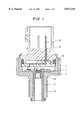
FIG. 1 is a cross-sectional view showing a pressure detecting apparatus in a first embodiment according to the present invention;
FIG. 2 is a fragmentary cross-sectional perspective view showing a sensing body and a strain gauge plate of the pressure detecting apparatus in the first embodiment;
FIG. 3A is a plane view showing a silicon substrate of the strain gauge plate in the first embodiment;
FIG. 3B is a cross-sectional view taken along a IIIB--IIIB line in FIG. 3A, showing the silicon substrate in the first embodiment;
FIG. 4 is a plane view showing diffusion gauges and diffusion leads formed on the silicon substrate in the first embodiment;
FIG. 5 is an explanatory view for explaining generation of stress with respect to a current direction when a diffusion gauge is formed on a {100} silicon substrate;
FIG. 6 is an electric connection view showing a Wheatstone bridge circuit composed of the diffusion gauges;
FIG. 7 is a plane view showing a silicon substrate of a strain gauge plate having a thin portion and a through hole in a modified embodiment;
FIG. 8 is a plane view showing a silicon substrate of a strain gauge plate having a thin portion and four through holes in a modified embodiment;
FIG. 9 is a cross-sectional view showing a silicon substrate of a strain gauge plate having a thin portion in a modified embodiment;
FIG. 10 is a cross-sectional view showing a sensing body and a strain gauge plate used in experiments to obtain a relationship in FIG. 11;
FIG. 11 is a graph showing a relationship between a magnitude of stress generated at the center of the strain gauge plate and a thickness of a glass base;
FIG. 12 is a fragmentary cross-sectional perspective view showing a sensing body and a strain gauge plate in the other embodiment;
FIG. 13 is a fragmentary cross-sectional perspective view showing a sensing body and a strain gauge plate in the other embodiment;
FIG. 14 is a fragmentary cross-sectional perspective view showing a sensing body and a strain gauge plate in the other embodiment;
FIG. 15A is a cross-sectional perspective view showing a sensing body and a strain gauge plate of a pressure detecting apparatus according to a prior art;
FIG. 15B is a graph showing a relationship between stress and a position of the strain gauge plate;
FIG. 15C is a cross-sectional perspective view showing sensing body and a strain gauge plate of a pressure detecting apparatus according to a prior art; and
FIG. 15D is a graph showing a relationship between stress and a position of the strain gauge plate.
DETAILED DESCRIPTION OF THE PREFERRED EMBODIMENTS
Embodiments according to the present invention will be described hereinunder with reference to the drawings.
A pressure detecting apparatus in a first embodiment detects pressure of fuel in a high pressure fuel injection apparatus, or of high pressure (10-200 MPa) fluid such as brake fluid, or the like.
As shown in FIG. 1, the pressure detecting apparatus has a metallic housing 1 and a cylindrical sensing body 2 inserted into the housing 1 and fixed at an opening end of the housing 1 by welding. The sensing body 2 is made of metal having low thermal expansion coefficient (covar, 42-alloy, or the like, the thermal expansion coefficient of which is close to that of silicon). A thin diaphragm 2a for receiving pressure is formed at the center of an upper face of the sensing body 2.
On the upper face of the diaphragm 2a is bonded a strain gauge plate 3 through a glass layer, or by utilizing a hard adhesive or the like. The strain gauge plate 3 has diffusion gauges for detecting the pressure applied to the diaphragm 2a.
A ring-shaped ceramic substrate 7 having an amplification circuit for amplifying an electric signal from the strain gauge plate 3 is disposed on the top of the housing 1 so as to surround the strain gauge plate 3. The electric signal amplified by the amplification circuit is output to the outside of the pressure detecting apparatus through a connector pin 8. The amplification circuit may be formed on the strain gauge plate 3.
A connector 9 made of resin is fixed to the housing 1 through an O-shaped ring 10 by caulking. The housing 1 has a threaded portion 1a, which is to be fixed by screwing to a pressure measurement portion of a measurement object.
FIG. 2 shows the sensing body 2 and the strain gauge plate 3 in cross-section perspectively. The strain gauge plate 3 includes a silicon substrate 31 and a glass base 32. The silicon substrate 31 is to be bonded by anode joining to the glass base 31 which is bonded on the diaphragm 2a through a glass layer 33 having a low melting point.
The silicon substrate 31 is an n-type or a p-type {100} semiconductor substrate (n-type in the embodiment) as shown in FIGS. 3A and 3B. The thickness of the silicon substrate 31 is approximately in the range of 0.2 mm-0.6 mm, and the area thereof is approximately in the range of 2 mm2 -5 mm2.
The silicon substrate 31 is etched from its back side to form a thin portion 311a (for example, the thickness of which is approximately 15-100 μm) by an anisotropic etching using a potassium hydroxide (KOH) based etching solution. The side face of the silicon substrate 31 formed by the etching approximately makes an angle of 54.7° with the base of the silicon substrate 31 as shown in FIG. 3B.
Through holes 312a are formed on the right and the left sides of the thin portion 311a so that the thin portion 311a has a beam structure. When the diaphragm 2a is displaced, the beam structure determines the direction of the tensile stress generated in the thin portion 311a. That is, when pressure is applied to the diaphragm 2a (a circular portion indicated by a broken line in FIG. 3A) of the sensing body 2, the diaphragm 2a is so bent as to transmit the stress to the silicon substrate 31 through the glass base 32, whereby the tensile stress generates on the entire surface of the strain gauge plate 3. In this case, because the strain gauge plate 31 has through holes 312a, the stress in the longitudinal direction becomes large and predominant compared to the stress in the lateral direction on the surface of the thin portion 311a.
Further, as shown in FIG. 4, p-type diffusion gauges 4a to 4d and diffusion leads 5a to 5h are formed on the surface of the silicon substrate 31 by diffusing an impurity. It is not necessary that the impurity concentration in the diffusion gauges 4a to 4d is equal to that in the diffusion leads 5a to 5h. The parts hatched in FIG. 4 are aluminum leads.
The longitudinal direction, that is, the direction in which a main current flows (hereinafter called a current direction), of the diffusion gauges 4a and 4d is parallel to the longitudinal direction (indicated by an arrow in FIG. 4) of the thin portion 311a. On the other hand, the current direction of the diffusion gauges 4b and 4c is parallel to the lateral direction of the thin portion 311a.
When a strip-shaped diffusion gauge is disposed on a {100} silicon substrate as shown in FIG. 5, a rate of change in resistance Δρ/ρ caused by piezoresistance effect is expressed by the following formula (1).
Δρ/ρ=π.sub.l σ.sub.l +π.sub.t σ.sub.t +π.sub.lt σ.sub.lt +π.sub.n σ.sub.n     (1)
wherein σl is a stress in the current direction (the longitudinal direction of the diffusion gauge), σt is a stress on the {100} face in a direction perpendicular to σl, σLt is a shearing stress on the {100} face, and σn is a stress in the normal direction of the {100} face.
Further, πl, πt, πlt, and πn are expressed by the following formulas (2).
π.sub.l =π.sub.l1 -2(π.sub.11 -π.sub.12 -π.sub.∴)·cos.sup.2 (φ+45°)·sin.sup.2 (φ+45°) π.sub.t =π.sub.l2 -2(π.sub.11 -π.sub.12 -π.sub.44)·cos.sup.2 (φ+45°)·sin.sup.2 (φ+45°) π.sub.lt =2(π.sub.11 -π.sub.12 -π.sub.44)·cos (φ+45°)·sin (φ+45°)·{-cos.sup.2 (φ+45°)+sin.sup.2 (φ+45°)}π.sub.n =π.sub.l2(2)
wherein φ is an angle between the <110> direction of the silicon substrate 31 and the current direction, and π11, π12, and π44 are coefficients for representing the piezoresistance effect, which changes in response to the conducting type of the diffusion gauge and the impurity concentration therein.
When the diffusion gauge is P type, π11, π12, π44 have the following relationship; π44 >>π11, πl2. Therefore, Δρ/ρ can be expressed by the following formula (3) by omitting π11 and π12 from the formulas (1) and (2).
Δρ/ρ=2π.sub.44 ·cos.sup.2 (φ+45°)·sin.sup.2 (φ+45°)·(σ.sub.l -σ.sub.t) -2π.sub.44 ·cos (φ+45°)·sin (φ+45°)·{-cos.sup.2 (φ+45°)+sin.sup.2 (φ+45°)}·σ.sub.lt               (3)
According to the formula (3), when φ is 0°, 90°, 180°, or 270° (that is, when the current direction is parallel to the <110> direction, Δρ/ρ is maximum and expressed by the following formula (4).
Δρ/ρ=π.sub.44 (σ.sub.l -σ.sub.t)/2(4)
When φ is 45°, 135°, 225°, or 315° (that is, when the current direction is parallel to the <100> direction), Δρ/ρ is minimum and expressed by the following formula (5).
Δρ/ρ=0                                       (5)
Therefore, when the diffusion gauges 4a to 4d are disposed so that each current direction of the diffusion gauges 4a to 4d is parallel to the <110> direction, the rate of change in the resistance caused by the piezoresistance effect Δρ/ρ can get its maximum value.
As mentioned above, the tensile stress occurs on the thin portion 311a in the direction indicated by an arrow in FIG. 4. The main currents of the diffusion gauges 4a and 4d flow in the stress direction in which the tensile stress occurs, respectively. Therefore, σl is larger than σt, whereby each resistance change rate of the diffusion gauges 4a and 4d gets a positive value according to the formula (4). As opposed to this, because the main currents of the diffusion gauges 4b and 4c flow in the direction perpendicular to the stress direction respectively, σl is smaller than σt. Therefore, each resistance change rate of the diffusion gauges 4b and 4c gets a negative value. As a result, when the stress occurs, the resistances of the diffusion gauges 4a and 4d increase, while the resistances of the diffusion gauges 4b and 4c decrease.
The diffusion gauges 4a to 4d form a Wheatstone bridge circuit shown in FIG. 6 to generate an output voltage VBC in response to the pressure applied to the diaphragm 2a. The output voltage VBC of the Wheatstone bridge can be expressed by the following formula (6) in the case that resistances re and rf of the diffusion leads 5e and 5f are very small enough to be ignored.
V.sub.BC =(Rb'·Rc'-Ra'·Rd')·V.sub.AD /(Ra'+Rb')·(Rc'+Rd')                             (6)
Further, Ra', Rb', Rc' and Rd' are expressed by the following formulas.
Ra'=Ra+ra.sub.1 +ra.sub.2
Rb'=Rb+rb.sub.1 +rb.sub.2
Rc'=Rc+rc.sub.1 +rc.sub.2
Rd'=Rd+rd.sub.1 +rd.sub.2
wherein Ra to Rd are resistances of the diffusion gauges 4a to 4d, respectively, and ra1 to rd1 are resistances of the diffusion leads 5a to 5d, respectively. Further, ra2 is a resistance of a portion where the diffusion lead 5g is connected to the diffusion gauge 4a, rb2 is a resistance of a portion where the diffusion lead 5g is connected to the diffusion gauge 4b, rc2 is a resistance of a portion where the diffusion lead 5h is connected to the diffusion gauge 4c, and rd2 is a resistance of a portion where the diffusion lead 5h is connected to the diffusion gauge 4d.
In the case that Ra' to Rd' are set to be R, respectively, when pressure is not applied to the diaphragm 2a, it is assumed that amounts of change of Ra' to Rd' in response to the change in pressure are ΔRa', ΔRd', -ΔRb', -ΔRC', respectively. All of ΔRa', ΔRd', ΔRb', and ΔRc' are positive values. In this case, ΔRa' to ΔRd' and R have the following relationship; ΔRa' to ΔRd'<<R. The output voltage VBC is expressed by the following formula (7).
V.sub.BC =-(ΔRa'+ΔRd'+ΔRb'+ΔRc')·R·V.sub.AD /(2R+ΔRa'-ΔRb')·(2R+ΔRd'-ΔRc')(7)
When ΔRa' to ΔRd' rectilinearly change with respect to the change in pressure, the numerator of the formula (7) indicates linearity. Therefore, when it is realized that; ΔRb'=ΔRa' and ΔRc'=ΔRd', the output voltage VBC has linearity with respect to the change in pressure. Accordingly, the amounts of the changes in the resistances of the diffusion gauges 4a and 4b are also set to be equal to each other and those of the diffusion gauges 4c and 4d are set to be equal to each other, thereby resulting in improvement of the linearity of the output voltage VBC.
In the above-mentioned constitution, in the case that the thin portion 311a is formed without having the through holes 312a, the stress occurs in the lateral direction with the same strength as in the longitudinal direction because of the symmetric property of the form. Therefore, the piezoresistance effect is set off, so that the output voltage VBC does not change.
In the embodiment, the through holes 312a are formed to form the thin portion 311a into the beam structure, whereby the direction in which the stress occurs is determined. Further, the direction in which the resistances of the diffusion gauges 4a and 4d change is set to be opposite to the direction in which the resistances of the diffusion gauges 4b and 4c change. As a result, the diffusion gauges can detect the pressure.
Because the diffusion leads 5a to 5h have a square shape, respectively, as shown in FIG. 4, the current flows in the diffusion leads 5a to 5h in the direction where a piezoresistance coefficient becomes minimum, that is, in the <100> direction of the silicon substrate. Accordingly, the changes in the resistances of the diffusion leads 5a to 5d with respect to the stress substantially become zero, resulting in improvement of the linearity of the output voltage VBC.
Only if the current flows within the diffusion leads 5a to 5h in the <100> direction, the linearity of the output voltage VBC is improved. Therefore, shapes of diffusion leads 5a to 5h are not limited to the square shape, and it may be the other shape. For example, a strip-shape elongating in parallel with the <100> direction of the silicon substrate may be adopted. The diffusion lead of the square shape, however, has small resistance compared with the diffusion lead of the strip-shape. Therefore, the voltage applied to the diffusion gauges through the diffusion lead having the square shape becomes large. As a result, the sensitivity of the sensor can be improved. To improve the linearity of the output voltage VBC, it is not necessary that the current flows exactly in the <100> direction in the diffusion leads. It is acceptable for the current to flow substantially in the <100> direction.
In the view that the current flows in the <100> direction in the diffusion leads, the diffusion leads arranged in this way may be adopted not only in the pressure sensor for detecting high pressure but in a pressure sensor for detecting low pressure or in an acceleration sensor with a beam formed on a {100} silicon substrate. Accordingly, the linearity of output voltage of the sensor can be improved.
Next, other embodiments having a thin portion of a different shape from that in the first embodiment will be described.
Although the thin portion 311a is formed so as to have two through holes 312a in the first embodiment, a thin portion 311b may be formed so as to have only one through hole 312b as shown in FIG. 7. In this case, the stress at the thin portion 311b is predominant in the longitudinal direction along the through hole 312b at the portion adjacent to the through hole 312b. The longer the distance to the through hole 312b becomes at the thin portion 311b, the larger the stress in the lateral direction becomes. Therefore, the diffusion gauges 4a to 4d are formed as adjacently to the through hole 312b as possible.
Further, as shown in FIG. 8, a thin portion 311c may be formed so as to have four through holes 312c. In this case, the stress occurs not only in the longitudinal direction but also in the lateral direction. In this constitution, when the diffusion gauges are disposed in the same arrangement as the first embodiment shown in FIG. 4, because each resistance of the diffusion gauges changes in the same direction from each other, the pressure can not be detected. Therefore, each diffusion gauge is formed on each beams, respectively, so that each longitudinal direction of the diffusion gauges is parallel to each other. As a result, the resistances of the diffusion gauges 4a and 4d change in the opposite direction to the direction in which the resistances of the diffusion gauges is 4b and 4c change, whereby the pressure can be detected.
In the embodiment shown in FIG. 7, because the thin portion 311b is supported at three sides, the thin portion 311b does not bend easily compared with the thin portion 311a in the first embodiment which is supported at only two sides as shown in FIG. 3. Therefore, the sensitivity of the thin portion 311b is inferior to that in the first embodiment.
Further, in the other embodiment shown in FIG. 8, because the diffusion gauges 4a to 4d are formed on the beams dispersively, it is difficult to connect wiring to each diffusion gauge. Further, if the accuracy processing the four through holes 312c is not sufficient, the sensitivity is lowered. Therefore, the sensitivity of the thin portion 311a having the two through holes 312a in the first embodiment is the best in the above mentioned three embodiments.
As shown in FIG. 9, in the case that a thin portion 311d is formed in the center being thinner than the periphery, the sensitivity with respect to the change in pressure can be improved.
In the present invention, it is not necessary that the silicon substrate 31 is bonded on the glass base 32. The silicon substrate 31 may be directly bonded on the sensing body 2 without the glass base 32 interposed therebetween.
Next, thermal stress caused by a difference in thermal expansion coefficient between the sensing body 2 and the strain gauge plate 3 will be explained. The inventors studied the relationship between the magnitude of the stress (thermal output) generated on the surface at the center of the strain gauge plate 3 and the thickness of the glass base 32, in a state that the strain gauge plate 3 was heated (ΔT=100° C.). The thickness of the silicon substrate 31 and the thickness of the diaphragm 2a were 0.3 mm, respectively, as shown in FIG. 10.
The result of the experiments is indicated in FIG. 11. Conventionally, it has been considered that the thermal output occurs even if the thickness of the glass base 32 is sufficiently thick. As indicated by a curved line A in FIG. 11, however, it was founded that there was a specific thickness of the glass base in which the thermal output became zero. In the case that the thickness of the glass base 32 is thinner than the specific thickness, the tensile stress is generated on the surface of the strain gauge plate 3 in response to the tensile stress generated on the diaphragm 2. In the case that the thickness of the glass base 32 is thicker than the specific thickness, the compressive stress is generated on the surface of the strain gauge plate 3 instead of the tensile stress. That is, the deformation mode of the strain gauge plate 3 changes on the basis of the thickness of the glass base 2.
The thicker the thickness of the glass base 32 becomes, the lower the sensitivity becomes as indicated by a curved line B in FIG. 11. However, when the thermal output which causes noise becomes zero the S/N ratio can be improved.
When the temperature of the strain gauge plate 3 and the sensing body 2 varies, the pattern of the curved line A changes, however, the thickness of the glass base 32 in which the thermal output becomes zero does not change. When the size of the silicon substrate 31 is changed, the curved line A moves in the left or the right direction in FIG. 11. Therefore, it is necessary that the ratio of the size of the silicon substrate 31 and the thickness of the glass base 32 are chosen appropriately so that the thermal output becomes zero.
To make the thermal output zero, as shown in FIGS. 12 and 13, a {110} silicon substrate without a thin portion as well as with the thin portion can be adopted to a pressure detecting apparatus. Further, as shown in FIG. 14, the {110} silicon substrate 31 without the thin portion may be directly bonded on the strain gauge plate 3 without the glass base 32.
In the above mentioned embodiments, the diffusion gauges 4a to 4d and the diffusion leads 5a to 5h may be n-type instead of p-type.
While the present invention has been shown and described with reference to the foregoing preferred embodiment, it will be apparent to those skilled in the art that changes in form and detail may be made therein without departing from the scope of the invention as defined in the appended claims.

Claims (22)

What is claimed is:
1. A pressure detecting apparatus comprising:
a diaphragm which is displaced in response to pressure applied thereto;
a silicon substrate provided on the diaphragm, said substrate having a thin portion which is displaced in response to the displacement of the diaphragm in order to generate stress therein, the thin portion having a through hole for determining a stress direction in which the stress occurs;
a first diffusion gauge disposed on the thin portion, a longitudinal direction of said first diffusion gauge being parallel to the stress direction so that a resistance of the first diffusion gauge changes in a positive direction in response to the stress; and
a second diffusion gauge disposed on the thin portion, a longitudinal direction of said second diffusion gauge being perpendicular to the stress direction so that a resistance of the second diffusion gauge changes in a negative direction in response to the same stress as imparted to the first diffusion gauge, wherein,
the pressure applied to the diaphragm is detected based on the resistances of the first and the second diffusion gauges.
2. A pressure detecting apparatus according to claim 1, a magnitude of change in the resistance of the first diffusion gauge is approximately equal to that of the second diffusion gauge.
3. A pressure detecting apparatus according to claim 1, further comprising diffusion leads connected with the first and the second diffusion gauges, respectively, for outputting an output value from the first and the second diffusion gauges, wherein,
the silicon substrate has {100} crystal orientation, and
main current of each of the diffusion leads flows in the <100> direction of the silicon substrate.
4. A pressure detecting apparatus according to claim 3 wherein the diffusion leads have a square-shape.
5. A pressure detecting apparatus according to claim 1, wherein:
the silicon substrate has {100} crystal orientation; and
main current of each of the first and the second diffusion gauges flows in the <110> direction of the silicon substrate.
6. A pressure detecting apparatus according to claim 1, wherein the thin portion has a beam structure, and the stress mainly occurs in a longitudinal direction of the thin portion.
7. A pressure detecting apparatus according to claim 6, wherein the through hole has a first and a second through holes so that the thin portion is formed therebetween.
8. A pressure detecting apparatus according to claim 6, wherein the silicon substrate has {100} crystal orientation, and the longitudinal direction of the thin portion is parallel to the <110> direction of the silicon substrate.
9. A pressure detecting apparatus comprising:
a diaphragm which is displaced in response to pressure applied thereto;
a silicon substrate provided on the diaphragm and having a thin portion which is displaced in response to the displacement of the diaphragm to generate stress, the thin portion having a through hole and being formed in a beam structure having a longitudinal direction in which the stress mainly occurs;
a first diffusion gauge formed on the thin portion, a main current thereof flowing in the longitudinal direction of the thin portion, and a resistance thereof changing in a positive direction in response to the stress; and
a second diffusion gauge formed on the thin portion, a main current thereof flowing in a direction perpendicular to the longitudinal direction of the thin portion, and a resistance thereof changing in a negative direction in response to the stress.
10. A pressure detecting apparatus comprising:
a diaphragm which is displaced in response to pressure applied thereto;
a substrate provided on the diaphragm and having a thin portion which is displaced in response to the displacement of the diaphragm to generate stress therein, the thin portion having a through hole for determining a direction in which the stress occurs, and being formed in a cross-shape with four beams; and
first and second diffusion gauges formed on the beams respectively, so that main current of each of the first and second diffusion gauges flows in parallel to each other,
wherein a resistance of the first diffusion gauge changes in a positive direction in response to the stress; and
a resistance of the second diffusion gauge changes in a negative direction in response to the stress.
11. A pressure detecting apparatus according to claim 10, wherein the first and the second diffusion gauges are formed so that main current of each of the diffusion gauges flows in parallel to the <110> direction of the silicon substrate.
12. A pressure detecting apparatus according to claim 1, wherein the thin portion has a beam structure, and the first and second diffusion gauges are perpendicular to each other.
13. A pressure detecting apparatus according to claim 1, wherein the thin portion has a cross-shape and the first and second diffusion gauges are parallel to each other.
14. A pressure detecting apparatus according to claim 9, wherein the silicon substrate has {100} crystal orientation, and the longitudinal direction of the thin portion is parallel to the <100> direction of the silicon substrate.
15. A pressure detecting apparatus according to claim 9, wherein the stress is tensile stress.
16. A pressure detecting apparatus according to claim 15, wherein a central portion of the thin portion is thinner than a peripheral portion thereof, and the first and second diffusion gauges are formed on the central portion of the thin portion.
17. A pressure detecting apparatus comprising:
a diaphragm which is displaced in response to pressure applied thereto;
a base disposed on the diaphragm;
a substrate disposed on the base and having a thin portion formed at a central portion thereof so that a gap is formed between the base and the substrate;
a through hole formed in the thin portion for determining a stress direction in which stress occurs in the thin portion when the thin portion is displaced in response to the displacement of the diaphragm transmitted via the base and a portion of the substrate surrounding the thin portion; and
a gauge provided on the thin portion, the gauge changing a resistance thereof in response to the stress of which a direction is determined by the through hole.
18. A pressure detecting apparatus according to claim 17, wherein:
the gauge includes first and second gauges;
a resistance of the first gauge increases in response to a change of the stress; and
a resistance of the second gauge decreases in response to the change of the stress.
19. A pressure detecting apparatus according to claim 18, wherein:
the thin portion has a beam shape by the through hole;
the first gauge is disposed to be parallel to a longitudinal direction of the thin portion; and
the second gauge is disposed to be perpendicular to the longitudinal direction of the thin portion.
20. A pressure detecting apparatus according to claim 19, wherein:
the substrate is a {100} crystal orientation silicon substrate; and
the longitudinal direction of the thin portion is parallel to the <110> direction of the silicon substrate.
21. A pressure detecting apparatus according to claim 18, wherein:
the thin portion has a cross-shape with four beams; and
the first and second gauges are respectively disposed on the beams to be parallel to each other.
22. A pressure detecting apparatus according to claim 21, wherein:
the substrate is a {100} crystal orientation silicon substrate; and
the beams of the thin portion are parallel to the <110> direction of the silicon substrate.
US08/805,171 1996-02-26 1997-02-24 Pressure detecting apparatus Expired - Fee Related US5872315A (en)

Applications Claiming Priority (2)

Application Number Priority Date Filing Date Title
JP8-38377 1996-02-26
JP8038377A JPH09232595A (en) 1996-02-26 1996-02-26 Pressure detection device

Publications (1)

Publication Number Publication Date
US5872315A true US5872315A (en) 1999-02-16

Family

ID=12523598

Family Applications (1)

Application Number Title Priority Date Filing Date
US08/805,171 Expired - Fee Related US5872315A (en) 1996-02-26 1997-02-24 Pressure detecting apparatus

Country Status (4)

Country Link
US (1) US5872315A (en)
EP (1) EP0793082B1 (en)
JP (1) JPH09232595A (en)
DE (1) DE69700021T2 (en)

Cited By (24)

* Cited by examiner, † Cited by third party
Publication number Priority date Publication date Assignee Title
US6595065B2 (en) 1997-07-25 2003-07-22 Denso Corporation Pressure detecting apparatus with metallic diaphragm
US20040007068A1 (en) * 2002-07-11 2004-01-15 Masaaki Tanaka Semiconductor dynamic quantity sensor
US6739199B1 (en) 2003-03-10 2004-05-25 Hewlett-Packard Development Company, L.P. Substrate and method of forming substrate for MEMS device with strain gage
US6782755B2 (en) * 2000-07-06 2004-08-31 California Institute Of Technology Surface-micromachined pressure sensor and high pressure application
US20040183150A1 (en) * 2003-03-19 2004-09-23 Asia Pacific Microsystems, Inc. Silicon pressure sensor and the manufacturing method thereof
US20060275143A1 (en) * 2005-05-20 2006-12-07 Copeland Corporation Sensor for hermetic machine
US20070095144A1 (en) * 2005-11-03 2007-05-03 Honeywell International Inc. Low cost high-pressure sensor
US20080202249A1 (en) * 2007-01-30 2008-08-28 Denso Corporation Semiconductor sensor and method of manufacturing the same
US20090060749A1 (en) * 2007-08-28 2009-03-05 Emerson Climate Technologies, Inc. Molded Plug For A Compressor
US20090212899A1 (en) * 2008-02-27 2009-08-27 Measurement Specialties, Inc. Low Pressure Transducer Using Beam and Diaphragm
US20090301212A1 (en) * 2006-07-19 2009-12-10 Continental Automotive Gmbh Pressure Sensing Device
US20110076162A1 (en) * 2009-03-27 2011-03-31 Heidecker Matthew J Compressor plug assembly
US20120075137A1 (en) * 2010-09-28 2012-03-29 Denso Corporation A/d converter circuit
US8262372B2 (en) 2007-05-10 2012-09-11 Emerson Climate Technologies, Inc. Compressor hermetic terminal
US9480177B2 (en) 2012-07-27 2016-10-25 Emerson Climate Technologies, Inc. Compressor protection module
US20160313199A1 (en) * 2013-11-20 2016-10-27 Hitachi Automotive Systems, Ltd. Pressure Sensor
CN106289624A (en) * 2016-11-07 2017-01-04 中国海洋大学 A kind of oceanic turbulence sensor based on MEMS
US20170038269A1 (en) * 2013-12-25 2017-02-09 Hitachi Automotive Systems ,Ltd. Pressure Measuring Device
US20170350782A1 (en) * 2016-06-03 2017-12-07 Honeywell International Inc. Fill fluid thermal expansion compensation for pressure sensors
CN108463704A (en) * 2016-01-14 2018-08-28 阿自倍尔株式会社 Pressure sensor
US20180310411A1 (en) * 2015-09-22 2018-10-25 At&S Austria Technologie & Systemtechnik Aktiengesellschaft Connection Panel for Electronic Components
US10704976B2 (en) 2015-12-28 2020-07-07 Azbil Corporation Pressure sensor
CN112484898A (en) * 2019-09-12 2021-03-12 威卡亚力山大维甘德欧洲两合公司 Bearing body with measuring element and method for producing a bearing body
US20210172816A1 (en) * 2019-12-04 2021-06-10 Siemens Aktiengesellschaft Multifunctional Sensor for the Process Industry

Families Citing this family (14)

* Cited by examiner, † Cited by third party
Publication number Priority date Publication date Assignee Title
DE10148859A1 (en) 2001-10-04 2003-04-10 Bosch Gmbh Robert Micromechanical component used in the production of a pressure sensor comprises a bellows-like structure with lateral twists parallel to both main surfaces of the component
JP2004101515A (en) * 2002-07-10 2004-04-02 Texas Instruments Inc Airtight pressure transducer
JP4828804B2 (en) * 2003-06-26 2011-11-30 京セラ株式会社 Ceramic diaphragm, manufacturing method thereof, and pressure sensor
JP4744088B2 (en) * 2004-02-24 2011-08-10 京セラ株式会社 Package for pressure detection device
DE102005058653A1 (en) * 2005-12-07 2007-06-28 Siemens Ag Medium pressure sensor e.g. relative pressure sensor, for air-conditioning system of motor vehicle, has sensor unit and circuit arrangement that are designed at side of sensor chip turned away from recess communicating with working medium
CN101379377B (en) * 2006-02-03 2011-05-11 弗兰霍菲尔运输应用研究公司 Deflectable micro-mechanical system and use thereof
JP5186725B2 (en) * 2006-03-15 2013-04-24 株式会社デンソー Pressure sensor
JP2008190394A (en) 2007-02-02 2008-08-21 Denso Corp Pressure sensor, and pressure control device
EP2138820B1 (en) 2008-06-25 2016-09-21 Sensata Technologies, Inc. A piezoresistive pressure-measuring plug for a combustion engine
JP5243988B2 (en) 2009-02-10 2013-07-24 本田技研工業株式会社 Multi-axis force sensor and acceleration sensor
DE102015104410B4 (en) 2015-03-24 2018-09-13 Tdk-Micronas Gmbh pressure sensor
US9964458B2 (en) * 2016-05-12 2018-05-08 Continental Automotive Systems, Inc. Pressure sensor device with anchors for die shrinkage and high sensitivity
DE102020105214A1 (en) * 2020-02-27 2021-09-02 Endress+Hauser SE+Co. KG Vibronic multi-sensor
DE102020105210A1 (en) 2020-02-27 2021-09-02 Tdk Electronics Ag Sensor and method of manufacturing a sensor

Citations (25)

* Cited by examiner, † Cited by third party
Publication number Priority date Publication date Assignee Title
US3922705A (en) * 1973-06-04 1975-11-25 Gen Electric Dielectrically isolated integral silicon diaphram or other semiconductor product
JPS5362581A (en) * 1976-11-17 1978-06-05 Hitachi Ltd Pressure detecting element
US4274423A (en) * 1977-12-15 1981-06-23 Kabushiki Kaisha Toyota Chuo Kenkyusho Catheter tip pressure transducer
US4498070A (en) * 1983-06-30 1985-02-05 Lirman Irving R Semi-conductor transducer and method of making the same
US4507170A (en) * 1980-01-07 1985-03-26 Myhre Kjell E Optimized stress and strain distribution diaphragms
JPS6188121A (en) * 1984-10-05 1986-05-06 Nippon Denso Co Ltd Pressure transducer
JPS6273131A (en) * 1985-09-26 1987-04-03 Nippon Soken Inc Pressure detector
US4712430A (en) * 1986-04-04 1987-12-15 Dynisco, Inc. Pressure transducer
JPS62291533A (en) * 1986-06-11 1987-12-18 Nippon Soken Inc Pressure detector
JPS635232A (en) * 1986-06-25 1988-01-11 Nippon Soken Inc Pressure detector
JPS6316240A (en) * 1986-07-08 1988-01-23 Nippon Soken Inc Pressure detector
JPS63196081A (en) * 1987-02-10 1988-08-15 Nippon Denso Co Ltd Semiconductor-type pressure detector
JPS63217671A (en) * 1987-03-05 1988-09-09 Nippon Denso Co Ltd Semiconductor pressure sensor
US4813286A (en) * 1986-07-18 1989-03-21 Vdo Adolf Schindling Ag Mechanical-electrical transducer
US4840067A (en) * 1986-06-13 1989-06-20 Nippon Soken, Inc. Semiconductor pressure sensor with method diaphragm
JPH01211986A (en) * 1988-02-19 1989-08-25 Matsushita Electric Ind Co Ltd Semiconductor pressure sensor
JPH02271234A (en) * 1989-04-12 1990-11-06 Nippon Soken Inc Pressure detector
JPH0328732A (en) * 1989-06-26 1991-02-06 Nippon Soken Inc Pressure detector and its manufacture
JPH0513782A (en) * 1991-07-04 1993-01-22 Nagano Keiki Seisakusho Ltd Metal diaphragm for pressure sensor
JPH0573551A (en) * 1991-09-11 1993-03-26 Toshiba Corp Electronic document review assistance device
US5207102A (en) * 1991-02-12 1993-05-04 Mitsubishi Denki Kabushiki Kaisha Semiconductor pressure sensor
US5291788A (en) * 1991-09-24 1994-03-08 Kabushiki Kaisha Toshiba Semiconductor pressure sensor
US5310610A (en) * 1988-05-07 1994-05-10 Sharp Kabushiki Kaisha Silicon micro sensor and manufacturing method therefor
US5483834A (en) * 1993-09-20 1996-01-16 Rosemount Inc. Suspended diaphragm pressure sensor
US5583296A (en) * 1993-01-19 1996-12-10 Fraunhofer-Gesellschaft Zur Forderung Der Angewandten Forschung E. V. Layered diaphragm pressure sensor with connecting channel

Patent Citations (26)

* Cited by examiner, † Cited by third party
Publication number Priority date Publication date Assignee Title
US3922705A (en) * 1973-06-04 1975-11-25 Gen Electric Dielectrically isolated integral silicon diaphram or other semiconductor product
JPS5362581A (en) * 1976-11-17 1978-06-05 Hitachi Ltd Pressure detecting element
US4274423A (en) * 1977-12-15 1981-06-23 Kabushiki Kaisha Toyota Chuo Kenkyusho Catheter tip pressure transducer
US4507170A (en) * 1980-01-07 1985-03-26 Myhre Kjell E Optimized stress and strain distribution diaphragms
US4498070A (en) * 1983-06-30 1985-02-05 Lirman Irving R Semi-conductor transducer and method of making the same
JPS6188121A (en) * 1984-10-05 1986-05-06 Nippon Denso Co Ltd Pressure transducer
JPS6273131A (en) * 1985-09-26 1987-04-03 Nippon Soken Inc Pressure detector
US4712430A (en) * 1986-04-04 1987-12-15 Dynisco, Inc. Pressure transducer
JPS62291533A (en) * 1986-06-11 1987-12-18 Nippon Soken Inc Pressure detector
US4986861A (en) * 1986-06-13 1991-01-22 Nippon Soken, Inc. Semiconductor pressure sensor and method for bonding semiconductor chip to metal diaphragm thereof
US4840067A (en) * 1986-06-13 1989-06-20 Nippon Soken, Inc. Semiconductor pressure sensor with method diaphragm
JPS635232A (en) * 1986-06-25 1988-01-11 Nippon Soken Inc Pressure detector
JPS6316240A (en) * 1986-07-08 1988-01-23 Nippon Soken Inc Pressure detector
US4813286A (en) * 1986-07-18 1989-03-21 Vdo Adolf Schindling Ag Mechanical-electrical transducer
JPS63196081A (en) * 1987-02-10 1988-08-15 Nippon Denso Co Ltd Semiconductor-type pressure detector
JPS63217671A (en) * 1987-03-05 1988-09-09 Nippon Denso Co Ltd Semiconductor pressure sensor
JPH01211986A (en) * 1988-02-19 1989-08-25 Matsushita Electric Ind Co Ltd Semiconductor pressure sensor
US5310610A (en) * 1988-05-07 1994-05-10 Sharp Kabushiki Kaisha Silicon micro sensor and manufacturing method therefor
JPH02271234A (en) * 1989-04-12 1990-11-06 Nippon Soken Inc Pressure detector
JPH0328732A (en) * 1989-06-26 1991-02-06 Nippon Soken Inc Pressure detector and its manufacture
US5207102A (en) * 1991-02-12 1993-05-04 Mitsubishi Denki Kabushiki Kaisha Semiconductor pressure sensor
JPH0513782A (en) * 1991-07-04 1993-01-22 Nagano Keiki Seisakusho Ltd Metal diaphragm for pressure sensor
JPH0573551A (en) * 1991-09-11 1993-03-26 Toshiba Corp Electronic document review assistance device
US5291788A (en) * 1991-09-24 1994-03-08 Kabushiki Kaisha Toshiba Semiconductor pressure sensor
US5583296A (en) * 1993-01-19 1996-12-10 Fraunhofer-Gesellschaft Zur Forderung Der Angewandten Forschung E. V. Layered diaphragm pressure sensor with connecting channel
US5483834A (en) * 1993-09-20 1996-01-16 Rosemount Inc. Suspended diaphragm pressure sensor

Cited By (44)

* Cited by examiner, † Cited by third party
Publication number Priority date Publication date Assignee Title
US6595065B2 (en) 1997-07-25 2003-07-22 Denso Corporation Pressure detecting apparatus with metallic diaphragm
US6782755B2 (en) * 2000-07-06 2004-08-31 California Institute Of Technology Surface-micromachined pressure sensor and high pressure application
US20040007068A1 (en) * 2002-07-11 2004-01-15 Masaaki Tanaka Semiconductor dynamic quantity sensor
US6898974B2 (en) 2002-07-11 2005-05-31 Denso Corporation Semiconductor dynamic quantity sensor
US6739199B1 (en) 2003-03-10 2004-05-25 Hewlett-Packard Development Company, L.P. Substrate and method of forming substrate for MEMS device with strain gage
US20040183150A1 (en) * 2003-03-19 2004-09-23 Asia Pacific Microsystems, Inc. Silicon pressure sensor and the manufacturing method thereof
US6838303B2 (en) * 2003-03-19 2005-01-04 Asia Pacific Microsystems, Inc. Silicon pressure sensor and the manufacturing method thereof
US7866964B2 (en) * 2005-05-20 2011-01-11 Emerson Climate Technologies, Inc. Sensor for hermetic machine
US20060275143A1 (en) * 2005-05-20 2006-12-07 Copeland Corporation Sensor for hermetic machine
US20070095144A1 (en) * 2005-11-03 2007-05-03 Honeywell International Inc. Low cost high-pressure sensor
US7260994B2 (en) 2005-11-03 2007-08-28 Honeywell International Inc. Low cost high-pressure sensor
CN101356426A (en) * 2005-11-03 2009-01-28 霍尼韦尔国际公司 Low cost high-voltage sensor
US20090301212A1 (en) * 2006-07-19 2009-12-10 Continental Automotive Gmbh Pressure Sensing Device
US7827867B2 (en) 2006-07-19 2010-11-09 Continental Automotive Gmbh Pressure sensing device
US7644623B2 (en) * 2007-01-30 2010-01-12 Denso Corporation Semiconductor sensor for measuring a physical quantity and method of manufacturing the same
US20080202249A1 (en) * 2007-01-30 2008-08-28 Denso Corporation Semiconductor sensor and method of manufacturing the same
US8262372B2 (en) 2007-05-10 2012-09-11 Emerson Climate Technologies, Inc. Compressor hermetic terminal
US8939734B2 (en) 2007-08-28 2015-01-27 Emerson Climate Technologies, Inc. Molded plug for a compressor
US20090060749A1 (en) * 2007-08-28 2009-03-05 Emerson Climate Technologies, Inc. Molded Plug For A Compressor
US20090212899A1 (en) * 2008-02-27 2009-08-27 Measurement Specialties, Inc. Low Pressure Transducer Using Beam and Diaphragm
WO2009108872A1 (en) * 2008-02-27 2009-09-03 Measurement Specialties, Inc. A low pressure transducer using beam and diaphragm
US20110076162A1 (en) * 2009-03-27 2011-03-31 Heidecker Matthew J Compressor plug assembly
US8939735B2 (en) 2009-03-27 2015-01-27 Emerson Climate Technologies, Inc. Compressor plug assembly
US8427352B2 (en) * 2010-09-28 2013-04-23 Denso Corporation A/D converter circuit including pulse circulation circuit with delay units coupled together in ring shape
US20120075137A1 (en) * 2010-09-28 2012-03-29 Denso Corporation A/d converter circuit
US9480177B2 (en) 2012-07-27 2016-10-25 Emerson Climate Technologies, Inc. Compressor protection module
US10485128B2 (en) 2012-07-27 2019-11-19 Emerson Climate Technologies, Inc. Compressor protection module
US10028399B2 (en) 2012-07-27 2018-07-17 Emerson Climate Technologies, Inc. Compressor protection module
US20160313199A1 (en) * 2013-11-20 2016-10-27 Hitachi Automotive Systems, Ltd. Pressure Sensor
US10060815B2 (en) * 2013-11-20 2018-08-28 Hitachi Automotive Systems, Ltd. Pressure sensor
US20170038269A1 (en) * 2013-12-25 2017-02-09 Hitachi Automotive Systems ,Ltd. Pressure Measuring Device
EP3088859A4 (en) * 2013-12-25 2017-04-19 Hitachi Automotive Systems, Ltd. Pressure measurement device
US10139300B2 (en) * 2013-12-25 2018-11-27 Hitachi Automotive Systems, Ltd. High pressure strain detection device with a base made of a first brittle material and a strain detection element bonded to the base via a second brittle material
US20180310411A1 (en) * 2015-09-22 2018-10-25 At&S Austria Technologie & Systemtechnik Aktiengesellschaft Connection Panel for Electronic Components
US10704976B2 (en) 2015-12-28 2020-07-07 Azbil Corporation Pressure sensor
CN108463704A (en) * 2016-01-14 2018-08-28 阿自倍尔株式会社 Pressure sensor
CN108463704B (en) * 2016-01-14 2020-02-07 阿自倍尔株式会社 Pressure sensor
US10890500B2 (en) 2016-01-14 2021-01-12 Azbil Corporation Pressure sensor
US20170350782A1 (en) * 2016-06-03 2017-12-07 Honeywell International Inc. Fill fluid thermal expansion compensation for pressure sensors
CN106289624A (en) * 2016-11-07 2017-01-04 中国海洋大学 A kind of oceanic turbulence sensor based on MEMS
CN112484898A (en) * 2019-09-12 2021-03-12 威卡亚力山大维甘德欧洲两合公司 Bearing body with measuring element and method for producing a bearing body
DE102019129411A1 (en) * 2019-09-12 2021-03-18 Wika Alexander Wiegand Se & Co. Kg Sensor body with a measuring element and manufacturing method for a sensor body
US20210172816A1 (en) * 2019-12-04 2021-06-10 Siemens Aktiengesellschaft Multifunctional Sensor for the Process Industry
US11703407B2 (en) * 2019-12-04 2023-07-18 Siemens Aktiengesellschaft Multifunctional sensor for the process industry

Also Published As

Publication number Publication date
EP0793082B1 (en) 1998-09-02
DE69700021D1 (en) 1998-10-08
EP0793082A1 (en) 1997-09-03
JPH09232595A (en) 1997-09-05
DE69700021T2 (en) 1999-01-21

Similar Documents

Publication Publication Date Title
US5872315A (en) Pressure detecting apparatus
JP2595829B2 (en) Differential pressure sensor and multifunction differential pressure sensor
US10724909B2 (en) Microelectromechanical scalable bulk-type piezoresistive force/pressure sensor
US5012677A (en) Differential pressure transmitter
JP5186725B2 (en) Pressure sensor
JPH0425735A (en) Semicondcutor diaphragm for measuring pressure and differential pressure
JP4337656B2 (en) Pressure sensor
US5537882A (en) Semiconductor sensor for detecting physical amount without thermal hypsteresis where output wiring is disposed in a stress insensitive direction
US3968466A (en) Pressure transducer
US20150276517A1 (en) Mechanical Quantity Measuring Device
US6097821A (en) Electrostatic capacitance type transducer
US5932809A (en) Sensor with silicon strain gage
US5412993A (en) Pressure detection gage for semiconductor pressure sensor
JPH09329516A (en) Semiconductor pressure sensor and composite transmitter using it
JP2009265012A (en) Semiconductor sensor
JPH0419495B2 (en)
JP2512220B2 (en) Multi-function sensor
JP2694593B2 (en) Semiconductor pressure sensor
JPH10142086A (en) Semiconductor pressure sensor, its manufacturing method, and differential pressure transmitter using the same
JPH1038731A (en) Semiconductor pressure detector
JP3105087B2 (en) Differential pressure detector
JPS6336155B2 (en)
JP2002350257A (en) Pressure sensor
JP2822613B2 (en) Semiconductor pressure sensor
JPH01114731A (en) Semiconductor pressure transducer

Legal Events

Date Code Title Description
AS Assignment

Owner name: DENSO CORPORATION, JAPAN

Free format text: ASSIGNMENT OF ASSIGNORS INTEREST;ASSIGNORS:NAGASE, KAZUYOSHI;BABA, HIRONOBU;IMAI, MASAHITO;AND OTHERS;REEL/FRAME:008410/0266

Effective date: 19970131

FEPP Fee payment procedure

Free format text: PAYOR NUMBER ASSIGNED (ORIGINAL EVENT CODE: ASPN); ENTITY STATUS OF PATENT OWNER: LARGE ENTITY

FPAY Fee payment

Year of fee payment: 4

FPAY Fee payment

Year of fee payment: 8

REMI Maintenance fee reminder mailed
LAPS Lapse for failure to pay maintenance fees
STCH Information on status: patent discontinuation

Free format text: PATENT EXPIRED DUE TO NONPAYMENT OF MAINTENANCE FEES UNDER 37 CFR 1.362

FP Lapsed due to failure to pay maintenance fee

Effective date: 20110216