US5871586A - Chemical vapor deposition - Google Patents
Chemical vapor deposition Download PDFInfo
- Publication number
- US5871586A US5871586A US08/833,766 US83376697A US5871586A US 5871586 A US5871586 A US 5871586A US 83376697 A US83376697 A US 83376697A US 5871586 A US5871586 A US 5871586A
- Authority
- US
- United States
- Prior art keywords
- chamber
- reaction chamber
- conduits
- precursors
- reactor
- Prior art date
- Legal status (The legal status is an assumption and is not a legal conclusion. Google has not performed a legal analysis and makes no representation as to the accuracy of the status listed.)
- Expired - Lifetime
Links
Images


Classifications
-
- C—CHEMISTRY; METALLURGY
- C23—COATING METALLIC MATERIAL; COATING MATERIAL WITH METALLIC MATERIAL; CHEMICAL SURFACE TREATMENT; DIFFUSION TREATMENT OF METALLIC MATERIAL; COATING BY VACUUM EVAPORATION, BY SPUTTERING, BY ION IMPLANTATION OR BY CHEMICAL VAPOUR DEPOSITION, IN GENERAL; INHIBITING CORROSION OF METALLIC MATERIAL OR INCRUSTATION IN GENERAL
- C23C—COATING METALLIC MATERIAL; COATING MATERIAL WITH METALLIC MATERIAL; SURFACE TREATMENT OF METALLIC MATERIAL BY DIFFUSION INTO THE SURFACE, BY CHEMICAL CONVERSION OR SUBSTITUTION; COATING BY VACUUM EVAPORATION, BY SPUTTERING, BY ION IMPLANTATION OR BY CHEMICAL VAPOUR DEPOSITION, IN GENERAL
- C23C16/00—Chemical coating by decomposition of gaseous compounds, without leaving reaction products of surface material in the coating, i.e. chemical vapour deposition [CVD] processes
- C23C16/44—Chemical coating by decomposition of gaseous compounds, without leaving reaction products of surface material in the coating, i.e. chemical vapour deposition [CVD] processes characterised by the method of coating
- C23C16/455—Chemical coating by decomposition of gaseous compounds, without leaving reaction products of surface material in the coating, i.e. chemical vapour deposition [CVD] processes characterised by the method of coating characterised by the method used for introducing gases into reaction chamber or for modifying gas flows in reaction chamber
- C23C16/45563—Gas nozzles
- C23C16/45574—Nozzles for more than one gas
-
- C—CHEMISTRY; METALLURGY
- C23—COATING METALLIC MATERIAL; COATING MATERIAL WITH METALLIC MATERIAL; CHEMICAL SURFACE TREATMENT; DIFFUSION TREATMENT OF METALLIC MATERIAL; COATING BY VACUUM EVAPORATION, BY SPUTTERING, BY ION IMPLANTATION OR BY CHEMICAL VAPOUR DEPOSITION, IN GENERAL; INHIBITING CORROSION OF METALLIC MATERIAL OR INCRUSTATION IN GENERAL
- C23C—COATING METALLIC MATERIAL; COATING MATERIAL WITH METALLIC MATERIAL; SURFACE TREATMENT OF METALLIC MATERIAL BY DIFFUSION INTO THE SURFACE, BY CHEMICAL CONVERSION OR SUBSTITUTION; COATING BY VACUUM EVAPORATION, BY SPUTTERING, BY ION IMPLANTATION OR BY CHEMICAL VAPOUR DEPOSITION, IN GENERAL
- C23C16/00—Chemical coating by decomposition of gaseous compounds, without leaving reaction products of surface material in the coating, i.e. chemical vapour deposition [CVD] processes
- C23C16/44—Chemical coating by decomposition of gaseous compounds, without leaving reaction products of surface material in the coating, i.e. chemical vapour deposition [CVD] processes characterised by the method of coating
- C23C16/455—Chemical coating by decomposition of gaseous compounds, without leaving reaction products of surface material in the coating, i.e. chemical vapour deposition [CVD] processes characterised by the method of coating characterised by the method used for introducing gases into reaction chamber or for modifying gas flows in reaction chamber
- C23C16/45514—Mixing in close vicinity to the substrate
-
- C—CHEMISTRY; METALLURGY
- C23—COATING METALLIC MATERIAL; COATING MATERIAL WITH METALLIC MATERIAL; CHEMICAL SURFACE TREATMENT; DIFFUSION TREATMENT OF METALLIC MATERIAL; COATING BY VACUUM EVAPORATION, BY SPUTTERING, BY ION IMPLANTATION OR BY CHEMICAL VAPOUR DEPOSITION, IN GENERAL; INHIBITING CORROSION OF METALLIC MATERIAL OR INCRUSTATION IN GENERAL
- C23C—COATING METALLIC MATERIAL; COATING MATERIAL WITH METALLIC MATERIAL; SURFACE TREATMENT OF METALLIC MATERIAL BY DIFFUSION INTO THE SURFACE, BY CHEMICAL CONVERSION OR SUBSTITUTION; COATING BY VACUUM EVAPORATION, BY SPUTTERING, BY ION IMPLANTATION OR BY CHEMICAL VAPOUR DEPOSITION, IN GENERAL
- C23C16/00—Chemical coating by decomposition of gaseous compounds, without leaving reaction products of surface material in the coating, i.e. chemical vapour deposition [CVD] processes
- C23C16/44—Chemical coating by decomposition of gaseous compounds, without leaving reaction products of surface material in the coating, i.e. chemical vapour deposition [CVD] processes characterised by the method of coating
- C23C16/455—Chemical coating by decomposition of gaseous compounds, without leaving reaction products of surface material in the coating, i.e. chemical vapour deposition [CVD] processes characterised by the method of coating characterised by the method used for introducing gases into reaction chamber or for modifying gas flows in reaction chamber
- C23C16/45563—Gas nozzles
- C23C16/45565—Shower nozzles
-
- C—CHEMISTRY; METALLURGY
- C23—COATING METALLIC MATERIAL; COATING MATERIAL WITH METALLIC MATERIAL; CHEMICAL SURFACE TREATMENT; DIFFUSION TREATMENT OF METALLIC MATERIAL; COATING BY VACUUM EVAPORATION, BY SPUTTERING, BY ION IMPLANTATION OR BY CHEMICAL VAPOUR DEPOSITION, IN GENERAL; INHIBITING CORROSION OF METALLIC MATERIAL OR INCRUSTATION IN GENERAL
- C23C—COATING METALLIC MATERIAL; COATING MATERIAL WITH METALLIC MATERIAL; SURFACE TREATMENT OF METALLIC MATERIAL BY DIFFUSION INTO THE SURFACE, BY CHEMICAL CONVERSION OR SUBSTITUTION; COATING BY VACUUM EVAPORATION, BY SPUTTERING, BY ION IMPLANTATION OR BY CHEMICAL VAPOUR DEPOSITION, IN GENERAL
- C23C16/00—Chemical coating by decomposition of gaseous compounds, without leaving reaction products of surface material in the coating, i.e. chemical vapour deposition [CVD] processes
- C23C16/44—Chemical coating by decomposition of gaseous compounds, without leaving reaction products of surface material in the coating, i.e. chemical vapour deposition [CVD] processes characterised by the method of coating
- C23C16/455—Chemical coating by decomposition of gaseous compounds, without leaving reaction products of surface material in the coating, i.e. chemical vapour deposition [CVD] processes characterised by the method of coating characterised by the method used for introducing gases into reaction chamber or for modifying gas flows in reaction chamber
- C23C16/45563—Gas nozzles
- C23C16/45572—Cooled nozzles
-
- C—CHEMISTRY; METALLURGY
- C30—CRYSTAL GROWTH
- C30B—SINGLE-CRYSTAL GROWTH; UNIDIRECTIONAL SOLIDIFICATION OF EUTECTIC MATERIAL OR UNIDIRECTIONAL DEMIXING OF EUTECTOID MATERIAL; REFINING BY ZONE-MELTING OF MATERIAL; PRODUCTION OF A HOMOGENEOUS POLYCRYSTALLINE MATERIAL WITH DEFINED STRUCTURE; SINGLE CRYSTALS OR HOMOGENEOUS POLYCRYSTALLINE MATERIAL WITH DEFINED STRUCTURE; AFTER-TREATMENT OF SINGLE CRYSTALS OR A HOMOGENEOUS POLYCRYSTALLINE MATERIAL WITH DEFINED STRUCTURE; APPARATUS THEREFOR
- C30B25/00—Single-crystal growth by chemical reaction of reactive gases, e.g. chemical vapour-deposition growth
- C30B25/02—Epitaxial-layer growth
- C30B25/14—Feed and outlet means for the gases; Modifying the flow of the reactive gases
Definitions
- This invention relates to chemical vapour deposition and more particularly, but not exclusively, is concerned with metal organic chemical vapour deposition (MOCVD).
- MOCVD metal organic chemical vapour deposition
- MOCVD is a well known technique which is ordinarily used to achieve epitaxial growth of semi-conductor and high temperature superconductor compounds such as GaAs, GaAlAs, InP and InGaAlP.
- appropriate precursors are mixed together and heated in the presence of a suitable substrate so that the compound is formed by reaction of the precursors and is deposited on the substrate such that the crystal orientation of the deposited layer is the same as that of the substrate.
- the resultant materials have a wide range of electronic and opto-electronic applications including the production of light emitting diodes (LEDs) and laser diodes.
- the wavelength of these devices is determined by the band gap of the deposited material which is dependent on its composition. Generally, for compositions containing Ga, Al, In, P and As, the emission is within the spectral range extending from green to the mid infra-red. Additionally, there is a requirement for emission in the blue region of the spectrum but there have been technological difficulties in fabricating devices within the group III-V semiconductor field despite the theoretical suitability of gallium nitride in particular. Consequently, other material systems have been used to manufacture blue devices such as SiC and ZnSe. These materials are not very efficient and there are process advantages in producing all devices from the same basic material system regardless of wavelength.
- a horizontal tube having an inlet zone at one end wherein the gaseous precursors are mixed and including a reaction chamber containing a heated horizontally disposed substrate so that the mixed precursors and a carrier gas from the inlet zone can pass over the substrate.
- the precursors are decomposed in the reaction chamber and deposit epitaxially on to the substrate.
- the reactor includes a vertical tube and the mixture of gaseous precursors is introduced in an inlet zone at the top. The gas mixture then passes down the tube and over a horizontally disposed substrate located in a reaction chamber and thence to an exhaust port in an outlet zone at the bottom of the tube. It is also known to provide multiple wafer designs wherein the substrate may be rotated to improve uniformity of thickness and composition of the deposited layer.
- the precursors used do not react together before the precursor mixture is heated.
- good mixing of the precursors (which is essential for good homogeneity in the deposited layer) can be achieved prior to the mixture being heated to form the desired material.
- the gaseous precursors are mixed together in a cold part of the reactor remotely from the heated substrate and are then conveyed together along a conduit to the heated substrate located in the reaction chamber.
- a first aspect of the present invention provides a reactor for producing a material from first and second gaseous precursors by chemical vapour deposition, which reactor comprises:
- reaction chamber for accommodating a heated substrate upon which said material is to be deposited by reaction of said precursors
- a method of producing a material by reaction of first and second gaseous precursors by chemical vapour deposition which method comprises cooling said first and second precursors, passing said cooled precursors separately along a plurality of discrete paths, and injecting said precursors into a reaction chamber containing a heated substrate upon which said material is to be deposited so that mixing of said precursors occurs in said reaction chamber in the presence of said substrate to form a deposit of said material on said substrate.
- One or both of the first and second precursors may be in the form of a single precursor or in the form of a mixture of substances which is chemically stable.
- the conduits of the first chamber pass through the second chamber in which case it is convenient for the first and second chambers to share a common dividing wall.
- the reactor includes an additional chamber for additional gas and a plurality of third conduits is provided between the third chamber and the reaction chamber to provide discrete paths along which the additional gas can pass to the reaction chamber.
- a plurality of third conduits is provided between the third chamber and the reaction chamber to provide discrete paths along which the additional gas can pass to the reaction chamber.
- reaction chamber may be such as to accommodate more than one substrate.
- FIG. 1 is a plan view of a MOCVD reactor in accordance with a first embodiment of the present invention
- FIG. 2 is a section through the reactor of FIG. 1 along the line B--B,
- FIG. 3 shows, on a larger scale, the part bounded by chain-dotted line X in FIG. 2,
- FIG. 4 is a section through the reactor of FIG. 1 along the line C--C,
- FIG. 5 is an underneath view of the reactor of FIG. 1 in the direction indicated by arrow A,
- FIG. 6 is a plan view of a reactor in accordance with a second embodiment of the present invention.
- FIG. 7 is a section through the reactor of FIG. 6 along line B--B,
- FIG. 8 is a section through the reactor of FIG. 6 along line C--C,
- FIG. 9 shows, on a larger scale, the part bounded by chain-dotted line Y in FIG. 8,
- FIG. 10 is an underneath view of the reactor of FIG. 6 in the direction of arrow A,
- FIG. 11 is a schematic vertical section through the upper part of a MOCVD reactor in accordance with a third embodiment of the present invention.
- FIG. 12 is a schematic vertical section through the lower part of the reactor of FIG. 11.
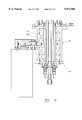
- the reactor comprises a generally vertical tube having cylindrical walls 1 typically formed of quartz. Located centrally within the tube is a susceptor (or thermal absorber) 2 mounted on a susceptor support 3.
- the susceptor 2 terminates in a horizontal surface upon which a substrate 4 (in the form of one or more wafers) is placed so that it can be heated by contact with the susceptor to a temperature above that at which the precursors decompose and react.
- the heating of the susceptor may be by, for example, induction heating, radiation heating or resistance heating as desired.
- the upper end of the reactor is closed by a closure assembly through which process and carrier gases may be introduced into the reactor chamber 5 located between the closure assembly and the horizontal surface of the susceptor where the MOCVD process takes place.
- the process and carrier gases are exhausted from the reactor chamber 5, typically at a reduced pressure, via a gap between a generally cylindrical liner 6 in the reactor and the susceptor support 3 and a means may be provided (not shown) to introduce a small flow of purging gas such as inert gas or hydrogen between the liner 6 and the reactor walls 1 and thence into the reactor chamber 5 for subsequent exhaustion between the liner 6 and the susceptor support 3.
- the purpose of the purge flow is to maintain the reactor chamber 5 in a clean condition and the liner 6 is suitably profiled so that the exhaust gases are symmetrically removed from the reactor chamber 5.
- the susceptor support 3 may include a means (not shown) of measuring the substrate temperature. If, however, the support is formed from quartz, the temperature may be measured optically. Also, if desired, the susceptor support 3 may be rotatable about the longitudinal axis of the tubular reactor so that the substrate is rotated during the MOCVD process. In this way, the uniformity of thickness and the uniformity of composition of the material deposited on the substrate can be improved.
- the closure assembly incorporates a means of introducing the carrier and precursor gases into the reactor chamber 5 while maintaining the gas integrity of the chamber.
- the closure assembly includes a top closure plate 7, an injector assembly 8, and a clamping ring 9.
- a seal 10, e.g. an O-ring seal is provided between the injector assembly 8 and the outer surface of the reactor wall 1
- a seal 11, e.g. an O-ring seal is provided between the injector assembly 8 and the free end of the reactor wall 1
- a seal 12 e.g. an O-ring seal
- the injector assembly 8 includes a tubular portion having cylindrical walls 14 and located co-axially with respect to reactor walls 1. Three plates which are preferably essentially circular, as shown, are sealed across the tubular portion 14 in spaced parallel relationship.
- the first (upper) plate 15 defines, with the top closure plate 7, a first chamber 16.
- the second (center) plate 17 defines, with the first plate 15 a second chamber 18.
- the third (lower) plate 19 forms, with the centre plate 17, a coolant chamber 20.
- the distance between the lower surface of plate 19 and the upper surface of the substrate 4 on the susceptor may be, for example, from 0.5 cm to 10 cm as desired.
- a plurality of first conduits 21 is provided between the first chamber 16 and the reaction chamber 5. They have inlets 22 located in the first chamber 16 and pass through chambers 18 and 20 without communicating therewith. They are bonded to the plates 15, 17 and 19 by, for example, vacuum brazing.
- the conduits terminate in outlets 23 in the form of injector nozzles in the reaction chamber 5 and provide a plurality of discrete paths from the first chamber 16 to the reaction chamber 5.
- a plurality of second conduits 24 is provided each having an inlet 25 in the second chamber 18 and an outlet 26 in the form of an injector nozzle in the reaction chamber 5. These conduits pass through the coolant chamber 20 without communicating with it and are bonded to the plates 17 and 19, by for example vacuum brazing.
- the outlets 23 and 26 of the first and second conduits 21 and 24 are uniformly distributed over the surface of the third plate 19 so that each outlet 23 is surrounded by several outlets 26 and vice versa.
- the injector assembly 8 includes (i) a first inlet 27 which is in communication with a gallery 28 in the injector assembly 8 which in turn communicates with the first chamber 16 (see FIG. 2) and (ii) a second inlet 29 which communicates with a gallery 30 in the injector assembly 8 which in turn communicates with the second chamber 18 (see FIG. 4).
- the first inlet 27 is for a first precursor (e.g. ammonia) and carrier gas and the second inlet 29 is for a second precursor (e.g. trimethyl or triethyl gallium) and carrier gas.
- the injector assembly 8 includes third and fourth inlets 31 and 32 for the introduction of coolant (e.g. water) into the assembly.
- the inlets 31 and 32 are in communication with galleries 33 and 34 respectively which in turn communicate with the coolant chamber 20.
- the injector assembly 8 also includes coolant outlets 35 and 36 which are similarly linked by galleries in the injector assembly 8 to the coolant chamber 20 whereby the coolant can be continuously passed through the injector assembly.
- the coolant passing through the coolant chamber 20 contacts the outer surfaces of the conduits 21 and 24 passing through the chamber 20 and thereby cools the gases passing through the conduits.
- the first precursor is injected into the reaction chamber 5 via inlet 27, first chamber 16 and first conduits 21 and the second precursor is injected into the reaction chamber 5 through inlet 29, second chamber 18 and second conduits 24.
- the precursors are separate and cool until they enter the reaction chamber 5.
- the conduit outlets over the bottom plate 19 the contact between the precursors can be minimized until they are close to the surface of the heated substrate 4. There they are rapidly mixed together to form a homogenous mixture because of the presence of the large number of injection points. This mixture is then presented to the heated substrate where the chemical vapour deposition reaction takes place. In the example, given, a uniform layer of gallium nitride is thus deposited on the surface of the substrate 4.
- FIGS. 6 to 10 parts corresponding to parts of FIGS. 1 to 5 are denoted by like reference numerals.
- the injector assembly 8 includes a further disc like plate 37 sealed across the tubular portion 14 so as to produce a third gas chamber 38 in the injector assembly.
- a plurality of third conduits 39 is provided having inlets 40 communicating with the third gas chamber 38 and outlets 41 in the form of nozzles communicating with the reaction chamber 5.
- the third conduits 39 are bonded to the plates through which they pass by, for example, vacuum brazing. Also, they do not communicate with chambers 16, 18 and 20.
- the injector assembly 8 includes a further inlet 42 communicating with a gallery 43 which in turn communicates with the chamber 38 whereby hydrogen or other suitable gas may be introduced into chamber 38.
- This gas then passes along the third conduits 39 and into the reaction chamber 5 without contact with the precursors until all three gases enter the reaction chamber 5.
- the location of the outlets 41 of the third conduits is such that the hydrogen emanating therefrom separates the precursor gas streams so that they do not contact one another at the injector nozzles 23 and 26. In this way, the possibility of surface enhanced reactions is reduced.
- FIGS. 11 and 12 parts corresponding to parts of FIGS. 1 to 10 are denoted by like reference numerals.
- the reactor comprises a generally vertical tube having cylindrical walls 1 formed of stainless steel provided with a quartz liner 6 suitably shaped to provide a uniform exhaust restriction 54.
- the walls 6 include water cooling chambers 50 linked to a water inlet and a water outlet whereby cooling water may be passed through the reactor walls.
- the upper end of the reactor is closed by a closure assembly of the general type described in FIGS. 2 to 5.
- the closure assembly includes a plurality of optical pyrometer ports 55 passing through the top closure plate 7 and through first plate 15, second plate 17, and third plate 19 and into the chamber 5.
- Each pyrometer port comprises a small diameter quartz rod 56 contained within a stainless steel tube 57 and used as an optical link to the pyrometer (not shown) for temperature measurement.
- the pyrometer is of a type which uses a broad band detector at wavelengths at which the substrate and deposited layers are transparent. In this way, interference effects are reduced. By having multiple pyrometer ports, temperature uniformity can be determined.
- Each port 55 includes an inlet 58 whereby a small quantity of hydrogen or inert gas can be introduced between the stainless steel tube 57 and the quartz rod 56 to prevent deposition (from the reactive gases used in the process) on the end of the quartz rod.
- the closure assembly includes first and second inlets 27 and 29, respectively, for introducing first and second gaseous precursors into the reaction chamber 5.
- First inlet 27 communicates with the first chamber 16 located between cover plate 7 and first plate 15 and linked to the reaction chamber 5 by first conduits 21.
- Second inlet 29 communicates with the second chamber 18 located between first plate 15 and second plate 17 and linked to the reaction chamber 5 by second conduits 24.
- the closure assembly includes an inlet 31 and an outlet 35 to enable water to be continuously passed through the injector assembly 8.
- a substrate 4 in the form of one or more wafers is located in the reaction chamber 5 and is mounted on a support hearth 61 manufactured from a material which is compatible with the reagents being used.
- a support hearth 61 manufactured from a material which is compatible with the reagents being used.
- graphite coated with silicone carbide is a typical material which may be used.
- the hearth 61 and any separate wafer holders which may be present are profiled so as to provide good temperature uniformity.
- the hearth 61 is mounted on a cylinder 62 attached to a rotating tube 63 of a double magnetic rotary seal 64 mounted for rotation on a static base plate 65.
- the support hearth 61, rotating tube 63, magnetic rotary seal 64 and base plate 65 effectively define an enclosure within which is contained a heater 66 manufactured from a refractory material, typically graphite.
- the heater is preferably in the form of a pancake induction coil and has a hot top surface to heat the support hearth 61 and robust integral terminals to enable electrical contact to be made at a cooler part of the heater.
- the heater may include separate sections so as to improve the temperature uniformity when large hearths are used to process multiple wafers.
- the enclosure protects the heater from the reagents being used and radiation shields 67 are provided to prevent heating of the magnetic rotary seal 64.
- the terminals of the heater 66 are electrically connected to water cooled electrical conductors 68.
- the enclosure for the heater 66 includes a port (not shown) in the base plate 65 whereby it may be purged with hydrogen or an inert gas.
- An exhaust port 69 is provided in communication with the reaction chamber 5 via the restriction 54. The exhaust port 69 may be in communication with the atmosphere or be connected to a low pressure exhaust system.
- the apparatus may be inverted so that the substrate 4 is facing downwards.
- first and second precursors are injected into the reaction chamber 5 via first and second inlets 27 and 29.
- the precursors are kept separate and cool until they enter the reaction chamber 5 and approach the surface of the heated wafer(s) where they are rapidly mixed together so that the chemical vapour deposition reaction takes place at the heated surface and a layer of the desired material is deposited on the surface.
Abstract
Description
Claims (4)
Priority Applications (1)
| Application Number | Priority Date | Filing Date | Title |
|---|---|---|---|
| US08/833,766 US5871586A (en) | 1994-06-14 | 1997-04-09 | Chemical vapor deposition |
Applications Claiming Priority (4)
| Application Number | Priority Date | Filing Date | Title |
|---|---|---|---|
| GB9411911 | 1994-06-14 | ||
| GB9411911A GB9411911D0 (en) | 1994-06-14 | 1994-06-14 | Improvements in or relating to chemical vapour deposition |
| US49031195A | 1995-06-14 | 1995-06-14 | |
| US08/833,766 US5871586A (en) | 1994-06-14 | 1997-04-09 | Chemical vapor deposition |
Related Parent Applications (1)
| Application Number | Title | Priority Date | Filing Date |
|---|---|---|---|
| US49031195A Continuation | 1994-06-14 | 1995-06-14 |
Publications (1)
| Publication Number | Publication Date |
|---|---|
| US5871586A true US5871586A (en) | 1999-02-16 |
Family
ID=10756709
Family Applications (1)
| Application Number | Title | Priority Date | Filing Date |
|---|---|---|---|
| US08/833,766 Expired - Lifetime US5871586A (en) | 1994-06-14 | 1997-04-09 | Chemical vapor deposition |
Country Status (5)
| Country | Link |
|---|---|
| US (1) | US5871586A (en) |
| EP (1) | EP0687749B1 (en) |
| JP (1) | JP3442536B2 (en) |
| DE (1) | DE69504762T2 (en) |
| GB (1) | GB9411911D0 (en) |
Cited By (266)
| Publication number | Priority date | Publication date | Assignee | Title |
|---|---|---|---|---|
| US6090210A (en) * | 1996-07-24 | 2000-07-18 | Applied Materials, Inc. | Multi-zone gas flow control in a process chamber |
| US6126753A (en) * | 1998-05-13 | 2000-10-03 | Tokyo Electron Limited | Single-substrate-processing CVD apparatus and method |
| US6153260A (en) * | 1997-04-11 | 2000-11-28 | Applied Materials, Inc. | Method for heating exhaust gas in a substrate reactor |
| EP1077274A1 (en) * | 1999-08-17 | 2001-02-21 | Applied Materials, Inc. | Lid cooling mechanism and method for optimized deposition of low-k dielectric using tri methylsilane-ozone based processes |
| WO2001057289A1 (en) * | 2000-02-04 | 2001-08-09 | Aixtron Ag | Device and method for depositing one or more layers onto a substrate |
| EP1134789A2 (en) * | 2000-03-16 | 2001-09-19 | Applied Materials, Inc. | One-piece dual gas faceplate for a showerhead in a semiconductor wafer processing system |
| US6402848B1 (en) * | 1999-04-23 | 2002-06-11 | Tokyo Electron Limited | Single-substrate-treating apparatus for semiconductor processing system |
| US6508197B1 (en) * | 1998-09-03 | 2003-01-21 | Cvc Products, Inc. | Apparatus for dispensing gas for fabricating substrates |
| WO2003071011A1 (en) * | 2002-02-22 | 2003-08-28 | Aixtron Ag | Method and device for depositing semi-conductor layers |
| US20040005731A1 (en) * | 2000-09-01 | 2004-01-08 | Holger Jurgensen | Device and method for the depostion of, in particular, crystalline layers on, in particular, crystalline substrates |
| WO2004097066A1 (en) | 2003-04-30 | 2004-11-11 | Aixtron Ag | Method and device for depositing semiconductor layers using two process gases, of which one is preconditioned |
| US20050020065A1 (en) * | 2002-02-06 | 2005-01-27 | Tokyo Electron Limited | Method of forming an oxidation-resistant TiSiN film |
| US20050106319A1 (en) * | 2002-04-22 | 2005-05-19 | Holger Jurgensen | Process and device for depositing thin layers on a substrate in a process chamber of adjustable height |
| US6916399B1 (en) * | 1999-06-03 | 2005-07-12 | Applied Materials Inc | Temperature controlled window with a fluid supply system |
| US20050263072A1 (en) * | 2004-05-26 | 2005-12-01 | Applied Materials, Inc. | Uniformity control for low flow process and chamber to chamber matching |
| US20050263248A1 (en) * | 2004-05-26 | 2005-12-01 | Applied Materials, Inc. | Blocker plate bypass to distribute gases in a chemical vapor deposition system |
| US20060021703A1 (en) * | 2004-07-29 | 2006-02-02 | Applied Materials, Inc. | Dual gas faceplate for a showerhead in a semiconductor wafer processing system |
| US20060021574A1 (en) * | 2004-08-02 | 2006-02-02 | Veeco Instruments Inc. | Multi-gas distribution injector for chemical vapor deposition reactors |
| US20060032736A1 (en) * | 2004-02-02 | 2006-02-16 | Lam Research Corporation | Deformation reduction at the main chamber |
| WO2006125777A1 (en) * | 2005-05-25 | 2006-11-30 | Lpe Spa | Device for introducing reaction gases into a reaction chamber and epitaxial reactor which uses said device |
| US7201942B2 (en) | 2000-02-16 | 2007-04-10 | Aixtron Ag | Coating method |
| DE102005055468A1 (en) * | 2005-11-22 | 2007-05-24 | Aixtron Ag | Coating one or more substrates comprises supplying gases to process chamber via chambers with gas outlet openings |
| US20070163440A1 (en) * | 2006-01-19 | 2007-07-19 | Atto Co., Ltd. | Gas separation type showerhead |
| US20070234956A1 (en) * | 2006-04-05 | 2007-10-11 | Dalton Jeremie J | Method and apparatus for providing uniform gas delivery to a reactor |
| US20080093341A1 (en) * | 2000-04-26 | 2008-04-24 | Unaxis Balzers Aktiengesellschaft | RF Plasma Reactor Having a Distribution Chamber with at Least One Grid |
| US20080156440A1 (en) * | 2001-09-10 | 2008-07-03 | Canon Anelva Corporation | Surface processing apparatus |
| WO2008148773A1 (en) | 2007-06-06 | 2008-12-11 | Aixtron Ag | Gas distributor comprising a plurality of diffusion-welded panes and a method for the production of such a gas distributor |
| US20080311294A1 (en) * | 2007-06-15 | 2008-12-18 | Hideki Ito | Vapor-phase growth apparatus and vapor-phase growth method |
| US20090013930A1 (en) * | 2005-01-31 | 2009-01-15 | Markus Reinhold | Gas distributor with pre-chambers disposed in planes |
| US20090095221A1 (en) * | 2007-10-16 | 2009-04-16 | Alexander Tam | Multi-gas concentric injection showerhead |
| US20090107403A1 (en) * | 2007-10-31 | 2009-04-30 | Moshtagh Vahid S | Brazed cvd shower head |
| US20090148704A1 (en) * | 2007-12-11 | 2009-06-11 | Sumitomo Electric Industries, Ltd. | Vapor-phase process apparatus, vapor-phase process method, and substrate |
| US20090149008A1 (en) * | 2007-10-05 | 2009-06-11 | Applied Materials, Inc. | Method for depositing group iii/v compounds |
| US20090159006A1 (en) * | 2006-05-09 | 2009-06-25 | Ulvac, Inc. | Thin film production apparatus and inner block for thin film production apparatus |
| US20090165713A1 (en) * | 2007-12-26 | 2009-07-02 | Samsung Electro-Mechanics Co, Ltd. | Chemical vapor deposition apparatus |
| US20090194024A1 (en) * | 2008-01-31 | 2009-08-06 | Applied Materials, Inc. | Cvd apparatus |
| US20090211707A1 (en) * | 2008-02-22 | 2009-08-27 | Hermes Systems Inc. | Apparatus for gas distribution and its applications |
| US20090260572A1 (en) * | 2008-04-18 | 2009-10-22 | Samsung Electro-Mechanics Co., Ltd. | Chemical vapor deposition apparatus |
| US20090260569A1 (en) * | 2008-04-18 | 2009-10-22 | Samsung Electro-Mechanics Co., Ltd. | Chemical vapor deposition apparatus |
| US20090266911A1 (en) * | 2008-04-24 | 2009-10-29 | Samsung Electro-Mechanics Co., Ltd. | Showerhead for chemical vapor deposition and chemical vapor deposition apparatus having the same |
| US20100071614A1 (en) * | 2008-09-22 | 2010-03-25 | Momentive Performance Materials, Inc. | Fluid distribution apparatus and method of forming the same |
| US20100215854A1 (en) * | 2007-06-24 | 2010-08-26 | Burrows Brian H | Hvpe showerhead design |
| US20100258049A1 (en) * | 2009-04-10 | 2010-10-14 | Applied Materials, Inc. | Hvpe chamber hardware |
| US20100263588A1 (en) * | 2009-04-15 | 2010-10-21 | Gan Zhiyin | Methods and apparatus for epitaxial growth of semiconductor materials |
| US20100273291A1 (en) * | 2009-04-28 | 2010-10-28 | Applied Materials, Inc. | Decontamination of mocvd chamber using nh3 purge after in-situ cleaning |
| US20100273318A1 (en) * | 2009-04-24 | 2010-10-28 | Applied Materials, Inc. | Substrate pretreatment for subsequent high temperature group iii depositions |
| US20100279020A1 (en) * | 2009-04-29 | 2010-11-04 | Applied Materials, Inc. | METHOD OF FORMING IN-SITU PRE-GaN DEPOSITION LAYER IN HVPE |
| US20110023782A1 (en) * | 2009-07-28 | 2011-02-03 | Ligadp Co., Ltd. | Gas injection unit for chemical vapor desposition apparatus |
| US20110030615A1 (en) * | 2009-08-04 | 2011-02-10 | Applied Materials, Inc. | Method and apparatus for dry cleaning a cooled showerhead |
| US20110143551A1 (en) * | 2008-04-28 | 2011-06-16 | Christophe Borean | Device and process for chemical vapor phase treatment |
| US20110277690A1 (en) * | 2010-05-14 | 2011-11-17 | Sierra Solar Power, Inc. | Multi-channel gas-delivery system |
| US20120045902A1 (en) * | 2007-03-30 | 2012-02-23 | Lam Research Corporation | Showerhead electrodes and showerhead electrode assemblies having low-particle performance for semiconductor material processing apparatuses |
| US20120067971A1 (en) * | 2009-06-01 | 2012-03-22 | Korea Institute of Industrial Tedhnology | Showerhead for film depositing vacuum equipment |
| US8183132B2 (en) | 2009-04-10 | 2012-05-22 | Applied Materials, Inc. | Methods for fabricating group III nitride structures with a cluster tool |
| US20120234945A1 (en) * | 2011-03-18 | 2012-09-20 | Applied Materials, Inc. | Multiple level showerhead design |
| US8298337B2 (en) | 2005-01-28 | 2012-10-30 | Aixtron, Inc. | Gas inlet element for a CVD reactor |
| US8361892B2 (en) | 2010-04-14 | 2013-01-29 | Applied Materials, Inc. | Multiple precursor showerhead with by-pass ports |
| US20130052804A1 (en) * | 2009-10-09 | 2013-02-28 | Applied Materials, Imn, | Multi-gas centrally cooled showerhead design |
| US20130118405A1 (en) * | 2011-11-10 | 2013-05-16 | Henry Ho | Fluid cooled showerhead with post injection mixing |
| CN103173742A (en) * | 2013-04-12 | 2013-06-26 | 光垒光电科技(上海)有限公司 | Spraying head and vapor deposition reaction cavity |
| US8778079B2 (en) | 2007-10-11 | 2014-07-15 | Valence Process Equipment, Inc. | Chemical vapor deposition reactor |
| CN103952685A (en) * | 2014-04-14 | 2014-07-30 | 南昌大学 | Metalorganic chemical vapor deposition (MOCVD) growth gas circuit capable of realizing free combination of indium gallium aluminum nitrogen material components and doping, and growth method |
| US20150007770A1 (en) * | 2013-07-03 | 2015-01-08 | Novellus Systems, Inc. | Multi-plenum, dual-temperature showerhead |
| US20150007771A1 (en) * | 2011-07-12 | 2015-01-08 | Aixtron Se | Gas inlet member of a cvd reactor |
| US20150187629A1 (en) * | 2013-12-31 | 2015-07-02 | Lam Research Ag | Apparatus for treating surfaces of wafer-shaped articles |
| US20150187624A1 (en) * | 2013-12-31 | 2015-07-02 | Lam Research Ag | Apparatus for treating surfaces of wafer-shaped articles |
| US9469542B2 (en) | 2014-06-06 | 2016-10-18 | Group Nanoxplore Inc. | Large scale production of thinned graphite, graphene, and graphite-graphene composites |
| US9586825B2 (en) | 2014-12-09 | 2017-03-07 | Group Nanoxplore Inc. | Large scale production of oxidized graphene |
| US20170096734A1 (en) * | 2012-05-18 | 2017-04-06 | Veeco Instruments Inc. | Rotating Disk Reactor With Ferrofluid Seal For Chemical Vapor Deposition |
| US9748434B1 (en) | 2016-05-24 | 2017-08-29 | Tesla, Inc. | Systems, method and apparatus for curing conductive paste |
| US9879359B2 (en) | 2013-06-21 | 2018-01-30 | Denso Corporation | Silicon carbide semiconductor film-forming apparatus and film-forming method using the same |
| US9954136B2 (en) | 2016-08-03 | 2018-04-24 | Tesla, Inc. | Cassette optimized for an inline annealing system |
| US9972740B2 (en) | 2015-06-07 | 2018-05-15 | Tesla, Inc. | Chemical vapor deposition tool and process for fabrication of photovoltaic structures |
| US10023959B2 (en) | 2015-05-26 | 2018-07-17 | Lam Research Corporation | Anti-transient showerhead |
| US10115856B2 (en) | 2016-10-31 | 2018-10-30 | Tesla, Inc. | System and method for curing conductive paste using induction heating |
| US10167552B2 (en) * | 2015-02-05 | 2019-01-01 | Lam Research Ag | Spin chuck with rotating gas showerhead |
| US10221482B2 (en) | 2013-02-15 | 2019-03-05 | Aixtron Se | Gas distributor for a CVD reactor |
| US10221483B2 (en) * | 2014-05-16 | 2019-03-05 | Applied Materials, Inc. | Showerhead design |
| US10316409B2 (en) | 2012-12-21 | 2019-06-11 | Novellus Systems, Inc. | Radical source design for remote plasma atomic layer deposition |
| CN110520966A (en) * | 2017-06-23 | 2019-11-29 | 昭和电工株式会社 | Film formation device |
| US10593546B2 (en) | 2015-08-14 | 2020-03-17 | Paragraf Ltd. | Method of producing a two-dimensional material |
| US10604841B2 (en) | 2016-12-14 | 2020-03-31 | Lam Research Corporation | Integrated showerhead with thermal control for delivering radical and precursor gas to a downstream chamber to enable remote plasma film deposition |
| US10808317B2 (en) | 2013-07-03 | 2020-10-20 | Lam Research Corporation | Deposition apparatus including an isothermal processing zone |
| US11015247B2 (en) | 2017-12-08 | 2021-05-25 | Lam Research Corporation | Integrated showerhead with improved hole pattern for delivering radical and precursor gas to a downstream chamber to enable remote plasma film deposition |
| US11164955B2 (en) | 2017-07-18 | 2021-11-02 | Asm Ip Holding B.V. | Methods for forming a semiconductor device structure and related semiconductor device structures |
| US11171025B2 (en) | 2019-01-22 | 2021-11-09 | Asm Ip Holding B.V. | Substrate processing device |
| US11168395B2 (en) | 2018-06-29 | 2021-11-09 | Asm Ip Holding B.V. | Temperature-controlled flange and reactor system including same |
| US20210384033A1 (en) * | 2020-06-03 | 2021-12-09 | Asm Ip Holding B.V. | Shower plate, substrate treatment device, and substrate treatment method |
| US11217444B2 (en) | 2018-11-30 | 2022-01-04 | Asm Ip Holding B.V. | Method for forming an ultraviolet radiation responsive metal oxide-containing film |
| US11222772B2 (en) | 2016-12-14 | 2022-01-11 | Asm Ip Holding B.V. | Substrate processing apparatus |
| USD940837S1 (en) | 2019-08-22 | 2022-01-11 | Asm Ip Holding B.V. | Electrode |
| US11227782B2 (en) | 2019-07-31 | 2022-01-18 | Asm Ip Holding B.V. | Vertical batch furnace assembly |
| US11227789B2 (en) | 2019-02-20 | 2022-01-18 | Asm Ip Holding B.V. | Method and apparatus for filling a recess formed within a substrate surface |
| US11230766B2 (en) | 2018-03-29 | 2022-01-25 | Asm Ip Holding B.V. | Substrate processing apparatus and method |
| US11233133B2 (en) | 2015-10-21 | 2022-01-25 | Asm Ip Holding B.V. | NbMC layers |
| US11232963B2 (en) | 2018-10-03 | 2022-01-25 | Asm Ip Holding B.V. | Substrate processing apparatus and method |
| US11242598B2 (en) | 2015-06-26 | 2022-02-08 | Asm Ip Holding B.V. | Structures including metal carbide material, devices including the structures, and methods of forming same |
| US11251035B2 (en) | 2016-12-22 | 2022-02-15 | Asm Ip Holding B.V. | Method of forming a structure on a substrate |
| US11251040B2 (en) | 2019-02-20 | 2022-02-15 | Asm Ip Holding B.V. | Cyclical deposition method including treatment step and apparatus for same |
| US11251068B2 (en) | 2018-10-19 | 2022-02-15 | Asm Ip Holding B.V. | Substrate processing apparatus and substrate processing method |
| USD944946S1 (en) | 2019-06-14 | 2022-03-01 | Asm Ip Holding B.V. | Shower plate |
| US11270899B2 (en) | 2018-06-04 | 2022-03-08 | Asm Ip Holding B.V. | Wafer handling chamber with moisture reduction |
| US11268192B2 (en) * | 2018-06-22 | 2022-03-08 | Samsung Display Co, Ltd. | Thin film processing apparatus and thin film processing method |
| US11274369B2 (en) | 2018-09-11 | 2022-03-15 | Asm Ip Holding B.V. | Thin film deposition method |
| US11282698B2 (en) | 2019-07-19 | 2022-03-22 | Asm Ip Holding B.V. | Method of forming topology-controlled amorphous carbon polymer film |
| US11286562B2 (en) | 2018-06-08 | 2022-03-29 | Asm Ip Holding B.V. | Gas-phase chemical reactor and method of using same |
| US11286558B2 (en) | 2019-08-23 | 2022-03-29 | Asm Ip Holding B.V. | Methods for depositing a molybdenum nitride film on a surface of a substrate by a cyclical deposition process and related semiconductor device structures including a molybdenum nitride film |
| US11289326B2 (en) | 2019-05-07 | 2022-03-29 | Asm Ip Holding B.V. | Method for reforming amorphous carbon polymer film |
| US11295980B2 (en) | 2017-08-30 | 2022-04-05 | Asm Ip Holding B.V. | Methods for depositing a molybdenum metal film over a dielectric surface of a substrate by a cyclical deposition process and related semiconductor device structures |
| US11296189B2 (en) | 2018-06-21 | 2022-04-05 | Asm Ip Holding B.V. | Method for depositing a phosphorus doped silicon arsenide film and related semiconductor device structures |
| USD947913S1 (en) | 2019-05-17 | 2022-04-05 | Asm Ip Holding B.V. | Susceptor shaft |
| US11306395B2 (en) | 2017-06-28 | 2022-04-19 | Asm Ip Holding B.V. | Methods for depositing a transition metal nitride film on a substrate by atomic layer deposition and related deposition apparatus |
| USD949319S1 (en) | 2019-08-22 | 2022-04-19 | Asm Ip Holding B.V. | Exhaust duct |
| US11315794B2 (en) | 2019-10-21 | 2022-04-26 | Asm Ip Holding B.V. | Apparatus and methods for selectively etching films |
| US11342216B2 (en) | 2019-02-20 | 2022-05-24 | Asm Ip Holding B.V. | Cyclical deposition method and apparatus for filling a recess formed within a substrate surface |
| US11339476B2 (en) | 2019-10-08 | 2022-05-24 | Asm Ip Holding B.V. | Substrate processing device having connection plates, substrate processing method |
| US11345999B2 (en) | 2019-06-06 | 2022-05-31 | Asm Ip Holding B.V. | Method of using a gas-phase reactor system including analyzing exhausted gas |
| US11355338B2 (en) | 2019-05-10 | 2022-06-07 | Asm Ip Holding B.V. | Method of depositing material onto a surface and structure formed according to the method |
| US11361990B2 (en) | 2018-05-28 | 2022-06-14 | Asm Ip Holding B.V. | Substrate processing method and device manufactured by using the same |
| US11374112B2 (en) | 2017-07-19 | 2022-06-28 | Asm Ip Holding B.V. | Method for depositing a group IV semiconductor and related semiconductor device structures |
| US11374172B2 (en) * | 2006-12-22 | 2022-06-28 | The Regents Of The University Of Michigan | Organic vapor jet deposition using an exhaust |
| US11378337B2 (en) | 2019-03-28 | 2022-07-05 | Asm Ip Holding B.V. | Door opener and substrate processing apparatus provided therewith |
| US11387120B2 (en) | 2017-09-28 | 2022-07-12 | Asm Ip Holding B.V. | Chemical dispensing apparatus and methods for dispensing a chemical to a reaction chamber |
| US11387106B2 (en) | 2018-02-14 | 2022-07-12 | Asm Ip Holding B.V. | Method for depositing a ruthenium-containing film on a substrate by a cyclical deposition process |
| US11390946B2 (en) | 2019-01-17 | 2022-07-19 | Asm Ip Holding B.V. | Methods of forming a transition metal containing film on a substrate by a cyclical deposition process |
| US11393690B2 (en) | 2018-01-19 | 2022-07-19 | Asm Ip Holding B.V. | Deposition method |
| US11390950B2 (en) | 2017-01-10 | 2022-07-19 | Asm Ip Holding B.V. | Reactor system and method to reduce residue buildup during a film deposition process |
| US11390945B2 (en) | 2019-07-03 | 2022-07-19 | Asm Ip Holding B.V. | Temperature control assembly for substrate processing apparatus and method of using same |
| US11398382B2 (en) | 2018-03-27 | 2022-07-26 | Asm Ip Holding B.V. | Method of forming an electrode on a substrate and a semiconductor device structure including an electrode |
| US11396702B2 (en) | 2016-11-15 | 2022-07-26 | Asm Ip Holding B.V. | Gas supply unit and substrate processing apparatus including the gas supply unit |
| US11401605B2 (en) | 2019-11-26 | 2022-08-02 | Asm Ip Holding B.V. | Substrate processing apparatus |
| US11411088B2 (en) | 2018-11-16 | 2022-08-09 | Asm Ip Holding B.V. | Methods for forming a metal silicate film on a substrate in a reaction chamber and related semiconductor device structures |
| US11410851B2 (en) | 2017-02-15 | 2022-08-09 | Asm Ip Holding B.V. | Methods for forming a metallic film on a substrate by cyclical deposition and related semiconductor device structures |
| US11414760B2 (en) | 2018-10-08 | 2022-08-16 | Asm Ip Holding B.V. | Substrate support unit, thin film deposition apparatus including the same, and substrate processing apparatus including the same |
| US11417545B2 (en) | 2017-08-08 | 2022-08-16 | Asm Ip Holding B.V. | Radiation shield |
| US11424119B2 (en) | 2019-03-08 | 2022-08-23 | Asm Ip Holding B.V. | Method for selective deposition of silicon nitride layer and structure including selectively-deposited silicon nitride layer |
| US11430674B2 (en) | 2018-08-22 | 2022-08-30 | Asm Ip Holding B.V. | Sensor array, apparatus for dispensing a vapor phase reactant to a reaction chamber and related methods |
| US11430640B2 (en) | 2019-07-30 | 2022-08-30 | Asm Ip Holding B.V. | Substrate processing apparatus |
| US11437241B2 (en) | 2020-04-08 | 2022-09-06 | Asm Ip Holding B.V. | Apparatus and methods for selectively etching silicon oxide films |
| US11443926B2 (en) | 2019-07-30 | 2022-09-13 | Asm Ip Holding B.V. | Substrate processing apparatus |
| US11447864B2 (en) | 2019-04-19 | 2022-09-20 | Asm Ip Holding B.V. | Layer forming method and apparatus |
| US11450529B2 (en) | 2019-11-26 | 2022-09-20 | Asm Ip Holding B.V. | Methods for selectively forming a target film on a substrate comprising a first dielectric surface and a second metallic surface |
| US11447861B2 (en) | 2016-12-15 | 2022-09-20 | Asm Ip Holding B.V. | Sequential infiltration synthesis apparatus and a method of forming a patterned structure |
| US11453943B2 (en) | 2016-05-25 | 2022-09-27 | Asm Ip Holding B.V. | Method for forming carbon-containing silicon/metal oxide or nitride film by ALD using silicon precursor and hydrocarbon precursor |
| USD965044S1 (en) | 2019-08-19 | 2022-09-27 | Asm Ip Holding B.V. | Susceptor shaft |
| USD965524S1 (en) | 2019-08-19 | 2022-10-04 | Asm Ip Holding B.V. | Susceptor support |
| US11469098B2 (en) | 2018-05-08 | 2022-10-11 | Asm Ip Holding B.V. | Methods for depositing an oxide film on a substrate by a cyclical deposition process and related device structures |
| US11476109B2 (en) | 2019-06-11 | 2022-10-18 | Asm Ip Holding B.V. | Method of forming an electronic structure using reforming gas, system for performing the method, and structure formed using the method |
| US11473195B2 (en) | 2018-03-01 | 2022-10-18 | Asm Ip Holding B.V. | Semiconductor processing apparatus and a method for processing a substrate |
| US11482418B2 (en) | 2018-02-20 | 2022-10-25 | Asm Ip Holding B.V. | Substrate processing method and apparatus |
| US11482412B2 (en) | 2018-01-19 | 2022-10-25 | Asm Ip Holding B.V. | Method for depositing a gap-fill layer by plasma-assisted deposition |
| US11482533B2 (en) | 2019-02-20 | 2022-10-25 | Asm Ip Holding B.V. | Apparatus and methods for plug fill deposition in 3-D NAND applications |
| US11488854B2 (en) | 2020-03-11 | 2022-11-01 | Asm Ip Holding B.V. | Substrate handling device with adjustable joints |
| US11488819B2 (en) | 2018-12-04 | 2022-11-01 | Asm Ip Holding B.V. | Method of cleaning substrate processing apparatus |
| US11492703B2 (en) | 2018-06-27 | 2022-11-08 | Asm Ip Holding B.V. | Cyclic deposition methods for forming metal-containing material and films and structures including the metal-containing material |
| US11495459B2 (en) | 2019-09-04 | 2022-11-08 | Asm Ip Holding B.V. | Methods for selective deposition using a sacrificial capping layer |
| US11499222B2 (en) | 2018-06-27 | 2022-11-15 | Asm Ip Holding B.V. | Cyclic deposition methods for forming metal-containing material and films and structures including the metal-containing material |
| US11501968B2 (en) | 2019-11-15 | 2022-11-15 | Asm Ip Holding B.V. | Method for providing a semiconductor device with silicon filled gaps |
| US11501973B2 (en) | 2018-01-16 | 2022-11-15 | Asm Ip Holding B.V. | Method for depositing a material film on a substrate within a reaction chamber by a cyclical deposition process and related device structures |
| US11501956B2 (en) | 2012-10-12 | 2022-11-15 | Asm Ip Holding B.V. | Semiconductor reaction chamber showerhead |
| US11499226B2 (en) | 2018-11-02 | 2022-11-15 | Asm Ip Holding B.V. | Substrate supporting unit and a substrate processing device including the same |
| US11515187B2 (en) | 2020-05-01 | 2022-11-29 | Asm Ip Holding B.V. | Fast FOUP swapping with a FOUP handler |
| US11515188B2 (en) | 2019-05-16 | 2022-11-29 | Asm Ip Holding B.V. | Wafer boat handling device, vertical batch furnace and method |
| US11521851B2 (en) | 2020-02-03 | 2022-12-06 | Asm Ip Holding B.V. | Method of forming structures including a vanadium or indium layer |
| US11527403B2 (en) | 2019-12-19 | 2022-12-13 | Asm Ip Holding B.V. | Methods for filling a gap feature on a substrate surface and related semiconductor structures |
| US11527400B2 (en) | 2019-08-23 | 2022-12-13 | Asm Ip Holding B.V. | Method for depositing silicon oxide film having improved quality by peald using bis(diethylamino)silane |
| US11530876B2 (en) | 2020-04-24 | 2022-12-20 | Asm Ip Holding B.V. | Vertical batch furnace assembly comprising a cooling gas supply |
| US11530483B2 (en) | 2018-06-21 | 2022-12-20 | Asm Ip Holding B.V. | Substrate processing system |
| US11532757B2 (en) | 2016-10-27 | 2022-12-20 | Asm Ip Holding B.V. | Deposition of charge trapping layers |
| US11551925B2 (en) | 2019-04-01 | 2023-01-10 | Asm Ip Holding B.V. | Method for manufacturing a semiconductor device |
| US11551912B2 (en) | 2020-01-20 | 2023-01-10 | Asm Ip Holding B.V. | Method of forming thin film and method of modifying surface of thin film |
| US11557474B2 (en) | 2019-07-29 | 2023-01-17 | Asm Ip Holding B.V. | Methods for selective deposition utilizing n-type dopants and/or alternative dopants to achieve high dopant incorporation |
| USD975665S1 (en) | 2019-05-17 | 2023-01-17 | Asm Ip Holding B.V. | Susceptor shaft |
| US11562901B2 (en) | 2019-09-25 | 2023-01-24 | Asm Ip Holding B.V. | Substrate processing method |
| US11572620B2 (en) | 2018-11-06 | 2023-02-07 | Asm Ip Holding B.V. | Methods for selectively depositing an amorphous silicon film on a substrate |
| US11581186B2 (en) | 2016-12-15 | 2023-02-14 | Asm Ip Holding B.V. | Sequential infiltration synthesis apparatus |
| US11587814B2 (en) | 2019-07-31 | 2023-02-21 | Asm Ip Holding B.V. | Vertical batch furnace assembly |
| US11587821B2 (en) | 2017-08-08 | 2023-02-21 | Asm Ip Holding B.V. | Substrate lift mechanism and reactor including same |
| US11587815B2 (en) | 2019-07-31 | 2023-02-21 | Asm Ip Holding B.V. | Vertical batch furnace assembly |
| USD979506S1 (en) | 2019-08-22 | 2023-02-28 | Asm Ip Holding B.V. | Insulator |
| US11594600B2 (en) | 2019-11-05 | 2023-02-28 | Asm Ip Holding B.V. | Structures with doped semiconductor layers and methods and systems for forming same |
| US11594450B2 (en) | 2019-08-22 | 2023-02-28 | Asm Ip Holding B.V. | Method for forming a structure with a hole |
| USD980813S1 (en) | 2021-05-11 | 2023-03-14 | Asm Ip Holding B.V. | Gas flow control plate for substrate processing apparatus |
| US11605528B2 (en) | 2019-07-09 | 2023-03-14 | Asm Ip Holding B.V. | Plasma device using coaxial waveguide, and substrate treatment method |
| USD980814S1 (en) | 2021-05-11 | 2023-03-14 | Asm Ip Holding B.V. | Gas distributor for substrate processing apparatus |
| US11610774B2 (en) | 2019-10-02 | 2023-03-21 | Asm Ip Holding B.V. | Methods for forming a topographically selective silicon oxide film by a cyclical plasma-enhanced deposition process |
| US11610775B2 (en) | 2016-07-28 | 2023-03-21 | Asm Ip Holding B.V. | Method and apparatus for filling a gap |
| USD981973S1 (en) | 2021-05-11 | 2023-03-28 | Asm Ip Holding B.V. | Reactor wall for substrate processing apparatus |
| US11615970B2 (en) | 2019-07-17 | 2023-03-28 | Asm Ip Holding B.V. | Radical assist ignition plasma system and method |
| US11626316B2 (en) | 2019-11-20 | 2023-04-11 | Asm Ip Holding B.V. | Method of depositing carbon-containing material on a surface of a substrate, structure formed using the method, and system for forming the structure |
| US11626308B2 (en) | 2020-05-13 | 2023-04-11 | Asm Ip Holding B.V. | Laser alignment fixture for a reactor system |
| US11629406B2 (en) | 2018-03-09 | 2023-04-18 | Asm Ip Holding B.V. | Semiconductor processing apparatus comprising one or more pyrometers for measuring a temperature of a substrate during transfer of the substrate |
| US11629407B2 (en) | 2019-02-22 | 2023-04-18 | Asm Ip Holding B.V. | Substrate processing apparatus and method for processing substrates |
| US11637014B2 (en) | 2019-10-17 | 2023-04-25 | Asm Ip Holding B.V. | Methods for selective deposition of doped semiconductor material |
| US11637011B2 (en) | 2019-10-16 | 2023-04-25 | Asm Ip Holding B.V. | Method of topology-selective film formation of silicon oxide |
| US11639548B2 (en) | 2019-08-21 | 2023-05-02 | Asm Ip Holding B.V. | Film-forming material mixed-gas forming device and film forming device |
| US11639811B2 (en) | 2017-11-27 | 2023-05-02 | Asm Ip Holding B.V. | Apparatus including a clean mini environment |
| US11643724B2 (en) | 2019-07-18 | 2023-05-09 | Asm Ip Holding B.V. | Method of forming structures using a neutral beam |
| US11646184B2 (en) | 2019-11-29 | 2023-05-09 | Asm Ip Holding B.V. | Substrate processing apparatus |
| US11646197B2 (en) | 2018-07-03 | 2023-05-09 | Asm Ip Holding B.V. | Method for depositing silicon-free carbon-containing film as gap-fill layer by pulse plasma-assisted deposition |
| US11644758B2 (en) | 2020-07-17 | 2023-05-09 | Asm Ip Holding B.V. | Structures and methods for use in photolithography |
| US11646204B2 (en) | 2020-06-24 | 2023-05-09 | Asm Ip Holding B.V. | Method for forming a layer provided with silicon |
| US11646205B2 (en) | 2019-10-29 | 2023-05-09 | Asm Ip Holding B.V. | Methods of selectively forming n-type doped material on a surface, systems for selectively forming n-type doped material, and structures formed using same |
| US11649546B2 (en) | 2016-07-08 | 2023-05-16 | Asm Ip Holding B.V. | Organic reactants for atomic layer deposition |
| US11658029B2 (en) | 2018-12-14 | 2023-05-23 | Asm Ip Holding B.V. | Method of forming a device structure using selective deposition of gallium nitride and system for same |
| US11658035B2 (en) | 2020-06-30 | 2023-05-23 | Asm Ip Holding B.V. | Substrate processing method |
| US11664267B2 (en) | 2019-07-10 | 2023-05-30 | Asm Ip Holding B.V. | Substrate support assembly and substrate processing device including the same |
| US11664245B2 (en) | 2019-07-16 | 2023-05-30 | Asm Ip Holding B.V. | Substrate processing device |
| US11664199B2 (en) | 2018-10-19 | 2023-05-30 | Asm Ip Holding B.V. | Substrate processing apparatus and substrate processing method |
| US11676812B2 (en) | 2016-02-19 | 2023-06-13 | Asm Ip Holding B.V. | Method for forming silicon nitride film selectively on top/bottom portions |
| US11674220B2 (en) | 2020-07-20 | 2023-06-13 | Asm Ip Holding B.V. | Method for depositing molybdenum layers using an underlayer |
| US11682572B2 (en) | 2017-11-27 | 2023-06-20 | Asm Ip Holdings B.V. | Storage device for storing wafer cassettes for use with a batch furnace |
| US11680839B2 (en) | 2019-08-05 | 2023-06-20 | Asm Ip Holding B.V. | Liquid level sensor for a chemical source vessel |
| USD990534S1 (en) | 2020-09-11 | 2023-06-27 | Asm Ip Holding B.V. | Weighted lift pin |
| US11685991B2 (en) | 2018-02-14 | 2023-06-27 | Asm Ip Holding B.V. | Method for depositing a ruthenium-containing film on a substrate by a cyclical deposition process |
| US11688603B2 (en) | 2019-07-17 | 2023-06-27 | Asm Ip Holding B.V. | Methods of forming silicon germanium structures |
| USD990441S1 (en) | 2021-09-07 | 2023-06-27 | Asm Ip Holding B.V. | Gas flow control plate |
| US11694892B2 (en) | 2016-07-28 | 2023-07-04 | Asm Ip Holding B.V. | Method and apparatus for filling a gap |
| US11705333B2 (en) | 2020-05-21 | 2023-07-18 | Asm Ip Holding B.V. | Structures including multiple carbon layers and methods of forming and using same |
| US11718913B2 (en) | 2018-06-04 | 2023-08-08 | Asm Ip Holding B.V. | Gas distribution system and reactor system including same |
| US11725277B2 (en) | 2011-07-20 | 2023-08-15 | Asm Ip Holding B.V. | Pressure transmitter for a semiconductor processing environment |
| US11725280B2 (en) | 2020-08-26 | 2023-08-15 | Asm Ip Holding B.V. | Method for forming metal silicon oxide and metal silicon oxynitride layers |
| US11735414B2 (en) | 2018-02-06 | 2023-08-22 | Asm Ip Holding B.V. | Method of post-deposition treatment for silicon oxide film |
| US11735445B2 (en) | 2018-10-31 | 2023-08-22 | Asm Ip Holding B.V. | Substrate processing apparatus for processing substrates |
| US11735422B2 (en) | 2019-10-10 | 2023-08-22 | Asm Ip Holding B.V. | Method of forming a photoresist underlayer and structure including same |
| US11742189B2 (en) | 2015-03-12 | 2023-08-29 | Asm Ip Holding B.V. | Multi-zone reactor, system including the reactor, and method of using the same |
| US11742198B2 (en) | 2019-03-08 | 2023-08-29 | Asm Ip Holding B.V. | Structure including SiOCN layer and method of forming same |
| US11749562B2 (en) | 2016-07-08 | 2023-09-05 | Asm Ip Holding B.V. | Selective deposition method to form air gaps |
| US11767589B2 (en) | 2020-05-29 | 2023-09-26 | Asm Ip Holding B.V. | Substrate processing device |
| US11769682B2 (en) | 2017-08-09 | 2023-09-26 | Asm Ip Holding B.V. | Storage apparatus for storing cassettes for substrates and processing apparatus equipped therewith |
| US11769670B2 (en) | 2018-12-13 | 2023-09-26 | Asm Ip Holding B.V. | Methods for forming a rhenium-containing film on a substrate by a cyclical deposition process and related semiconductor device structures |
| US11776846B2 (en) | 2020-02-07 | 2023-10-03 | Asm Ip Holding B.V. | Methods for depositing gap filling fluids and related systems and devices |
| US11781221B2 (en) | 2019-05-07 | 2023-10-10 | Asm Ip Holding B.V. | Chemical source vessel with dip tube |
| US11781243B2 (en) | 2020-02-17 | 2023-10-10 | Asm Ip Holding B.V. | Method for depositing low temperature phosphorous-doped silicon |
| US11795545B2 (en) | 2014-10-07 | 2023-10-24 | Asm Ip Holding B.V. | Multiple temperature range susceptor, assembly, reactor and system including the susceptor, and methods of using the same |
| US11804388B2 (en) | 2018-09-11 | 2023-10-31 | Asm Ip Holding B.V. | Substrate processing apparatus and method |
| US11802338B2 (en) | 2017-07-26 | 2023-10-31 | Asm Ip Holding B.V. | Chemical treatment, deposition and/or infiltration apparatus and method for using the same |
| US11804364B2 (en) | 2020-05-19 | 2023-10-31 | Asm Ip Holding B.V. | Substrate processing apparatus |
| US11810788B2 (en) | 2016-11-01 | 2023-11-07 | Asm Ip Holding B.V. | Methods for forming a transition metal niobium nitride film on a substrate by atomic layer deposition and related semiconductor device structures |
| US11814747B2 (en) | 2019-04-24 | 2023-11-14 | Asm Ip Holding B.V. | Gas-phase reactor system-with a reaction chamber, a solid precursor source vessel, a gas distribution system, and a flange assembly |
| US11823876B2 (en) | 2019-09-05 | 2023-11-21 | Asm Ip Holding B.V. | Substrate processing apparatus |
| US11821078B2 (en) | 2020-04-15 | 2023-11-21 | Asm Ip Holding B.V. | Method for forming precoat film and method for forming silicon-containing film |
| US11823866B2 (en) | 2020-04-02 | 2023-11-21 | Asm Ip Holding B.V. | Thin film forming method |
| US11828707B2 (en) | 2020-02-04 | 2023-11-28 | Asm Ip Holding B.V. | Method and apparatus for transmittance measurements of large articles |
| US11830738B2 (en) | 2020-04-03 | 2023-11-28 | Asm Ip Holding B.V. | Method for forming barrier layer and method for manufacturing semiconductor device |
| US11827981B2 (en) | 2020-10-14 | 2023-11-28 | Asm Ip Holding B.V. | Method of depositing material on stepped structure |
| US11830730B2 (en) | 2017-08-29 | 2023-11-28 | Asm Ip Holding B.V. | Layer forming method and apparatus |
| US11840761B2 (en) | 2019-12-04 | 2023-12-12 | Asm Ip Holding B.V. | Substrate processing apparatus |
| US11848200B2 (en) | 2017-05-08 | 2023-12-19 | Asm Ip Holding B.V. | Methods for selectively forming a silicon nitride film on a substrate and related semiconductor device structures |
| US11876356B2 (en) | 2020-03-11 | 2024-01-16 | Asm Ip Holding B.V. | Lockout tagout assembly and system and method of using same |
| US11873557B2 (en) | 2020-10-22 | 2024-01-16 | Asm Ip Holding B.V. | Method of depositing vanadium metal |
| US11885020B2 (en) | 2020-12-22 | 2024-01-30 | Asm Ip Holding B.V. | Transition metal deposition method |
| US11885013B2 (en) | 2019-12-17 | 2024-01-30 | Asm Ip Holding B.V. | Method of forming vanadium nitride layer and structure including the vanadium nitride layer |
| US11887857B2 (en) | 2020-04-24 | 2024-01-30 | Asm Ip Holding B.V. | Methods and systems for depositing a layer comprising vanadium, nitrogen, and a further element |
| US11885023B2 (en) | 2018-10-01 | 2024-01-30 | Asm Ip Holding B.V. | Substrate retaining apparatus, system including the apparatus, and method of using same |
| USD1012873S1 (en) | 2020-09-24 | 2024-01-30 | Asm Ip Holding B.V. | Electrode for semiconductor processing apparatus |
| US11891696B2 (en) | 2020-11-30 | 2024-02-06 | Asm Ip Holding B.V. | Injector configured for arrangement within a reaction chamber of a substrate processing apparatus |
| US11898243B2 (en) | 2020-04-24 | 2024-02-13 | Asm Ip Holding B.V. | Method of forming vanadium nitride-containing layer |
| US11901179B2 (en) | 2020-10-28 | 2024-02-13 | Asm Ip Holding B.V. | Method and device for depositing silicon onto substrates |
| US11923190B2 (en) | 2018-07-03 | 2024-03-05 | Asm Ip Holding B.V. | Method for depositing silicon-free carbon-containing film as gap-fill layer by pulse plasma-assisted deposition |
| US11923181B2 (en) | 2019-11-29 | 2024-03-05 | Asm Ip Holding B.V. | Substrate processing apparatus for minimizing the effect of a filling gas during substrate processing |
| US11929251B2 (en) | 2019-12-02 | 2024-03-12 | Asm Ip Holding B.V. | Substrate processing apparatus having electrostatic chuck and substrate processing method |
| US11939673B2 (en) | 2018-02-23 | 2024-03-26 | Asm Ip Holding B.V. | Apparatus for detecting or monitoring for a chemical precursor in a high temperature environment |
| US11946137B2 (en) | 2020-12-16 | 2024-04-02 | Asm Ip Holding B.V. | Runout and wobble measurement fixtures |
| US11956977B2 (en) | 2015-12-29 | 2024-04-09 | Asm Ip Holding B.V. | Atomic layer deposition of III-V compounds to form V-NAND devices |
| US11959171B2 (en) | 2022-07-18 | 2024-04-16 | Asm Ip Holding B.V. | Methods of forming a transition metal containing film on a substrate by a cyclical deposition process |
Families Citing this family (26)
| Publication number | Priority date | Publication date | Assignee | Title |
|---|---|---|---|---|
| KR100474791B1 (en) * | 1996-05-10 | 2005-06-27 | 스미또모 가가꾸 가부시키가이샤 | Manufacturing method of compound semiconductor |
| EP0946782A1 (en) * | 1996-11-27 | 1999-10-06 | Emcore Corporation | Chemical vapor deposition apparatus |
| GB9712400D0 (en) * | 1997-06-16 | 1997-08-13 | Trikon Equip Ltd | Shower head |
| US6148761A (en) * | 1998-06-16 | 2000-11-21 | Applied Materials, Inc. | Dual channel gas distribution plate |
| US6080241A (en) * | 1998-09-02 | 2000-06-27 | Emcore Corporation | Chemical vapor deposition chamber having an adjustable flow flange |
| US6364954B2 (en) | 1998-12-14 | 2002-04-02 | Applied Materials, Inc. | High temperature chemical vapor deposition chamber |
| DE10118130A1 (en) * | 2001-04-11 | 2002-10-17 | Aixtron Ag | Device for depositing crystalline layers on crystalline substrates in the gas phase comprises a heated reaction chamber with substrate holders arranged in a circular manner on a support, heated sources, and a hydride feed line |
| KR100408519B1 (en) * | 2001-05-03 | 2003-12-06 | 삼성전자주식회사 | Reaction chamber for atomic layer deposition |
| SG125069A1 (en) | 2001-05-17 | 2006-09-29 | Sumitomo Chemical Co | Method and system for manufacturing III-V group compound semiconductor and III-V group compound semiconductor |
| KR100782529B1 (en) * | 2001-11-08 | 2007-12-06 | 에이에스엠지니텍코리아 주식회사 | Apparatus for depositing |
| JP4324663B2 (en) * | 2002-09-05 | 2009-09-02 | 独立行政法人産業技術総合研究所 | Shower head and semiconductor heat treatment apparatus using shower head |
| JP5055044B2 (en) * | 2007-07-05 | 2012-10-24 | ニッコーシ株式会社 | Multi-shower head for multi-layer CVD |
| JP5143689B2 (en) * | 2007-09-27 | 2013-02-13 | シャープ株式会社 | Vapor phase growth apparatus and semiconductor device manufacturing method |
| JP5172617B2 (en) * | 2007-11-12 | 2013-03-27 | シャープ株式会社 | Vapor growth apparatus and vapor growth method |
| KR101376336B1 (en) | 2007-11-27 | 2014-03-18 | 한국에이에스엠지니텍 주식회사 | Atomic layer deposition apparatus |
| US8273178B2 (en) | 2008-02-28 | 2012-09-25 | Asm Genitech Korea Ltd. | Thin film deposition apparatus and method of maintaining the same |
| JP5015085B2 (en) * | 2008-07-15 | 2012-08-29 | シャープ株式会社 | Vapor growth equipment |
| JP4576466B2 (en) * | 2009-03-27 | 2010-11-10 | シャープ株式会社 | Vapor growth apparatus and vapor growth method |
| JP4699545B2 (en) * | 2009-07-06 | 2011-06-15 | シャープ株式会社 | Vapor growth apparatus and vapor growth method |
| DE102009043848A1 (en) | 2009-08-25 | 2011-03-03 | Aixtron Ag | CVD method and CVD reactor |
| JP4840832B2 (en) | 2010-04-28 | 2011-12-21 | シャープ株式会社 | Vapor phase growth apparatus, vapor phase growth method, and semiconductor device manufacturing method |
| KR101297933B1 (en) | 2010-07-12 | 2013-08-19 | 가부시키가이샤 알박 | Film-forming apparatus |
| JP2012216744A (en) * | 2010-11-10 | 2012-11-08 | Sharp Corp | Vapor growth device and vapor growth method |
| DE102011002145B4 (en) | 2011-04-18 | 2023-02-09 | Aixtron Se | Device and method for large-area deposition of semiconductor layers with gas-separated HCl feed |
| FR3029939A1 (en) | 2014-12-16 | 2016-06-17 | Saint-Gobain Lumilog | CHEMICAL VAPOR DEPOSITION REACTOR |
| DE202017105481U1 (en) | 2017-09-11 | 2018-12-12 | Aixtron Se | Gas inlet member for a CVD or PVD reactor |
Citations (21)
| Publication number | Priority date | Publication date | Assignee | Title |
|---|---|---|---|---|
| US3854443A (en) * | 1973-12-19 | 1974-12-17 | Intel Corp | Gas reactor for depositing thin films |
| US4051382A (en) * | 1975-07-18 | 1977-09-27 | Tokyo Shibaura Electric Co., Ltd. | Activated gas reaction apparatus |
| US4340568A (en) * | 1976-01-13 | 1982-07-20 | The Research Institute For Iron, Steel And Other Metals Of The Tohoku University | Super hard highly pure silicon nitrides and a process and apparatus for producing the same |
| US4368689A (en) * | 1980-12-29 | 1983-01-18 | Rockwell International Corporation | Beam source for deposition of thin film alloys |
| US4468283A (en) * | 1982-12-17 | 1984-08-28 | Irfan Ahmed | Method for etching and controlled chemical vapor deposition |
| JPS6065798A (en) * | 1983-09-19 | 1985-04-15 | Toyota Central Res & Dev Lab Inc | Growing of gallium nitride single crystal |
| JPS60175412A (en) * | 1984-02-21 | 1985-09-09 | Matsushita Electric Ind Co Ltd | Growing method of gallium nitride |
| JPS60207332A (en) * | 1984-03-30 | 1985-10-18 | Matsushita Electric Ind Co Ltd | Growth of gallium nitride |
| US4574093A (en) * | 1983-12-30 | 1986-03-04 | At&T Bell Laboratories | Deposition technique |
| JPS61101020A (en) * | 1984-10-24 | 1986-05-19 | Hitachi Ltd | Treating apparatus |
| JPH01223724A (en) * | 1988-03-02 | 1989-09-06 | Mitsubishi Electric Corp | Chemical vapor growth device |
| GB2219311A (en) * | 1988-05-06 | 1989-12-06 | Elektromat Veb | Gas inlet and discharge attachment for the gas-phase processing of workpieces |
| US4951603A (en) * | 1988-09-12 | 1990-08-28 | Daidousanso Co., Ltd. | Apparatus for producing semiconductors |
| JPH02234419A (en) * | 1989-03-07 | 1990-09-17 | Koujiyundo Kagaku Kenkyusho:Kk | Plasma electrode |
| US4997677A (en) * | 1987-08-31 | 1991-03-05 | Massachusetts Institute Of Technology | Vapor phase reactor for making multilayer structures |
| JPH03170675A (en) * | 1989-11-28 | 1991-07-24 | Mitsubishi Electric Corp | Chemical vapor growth method |
| US5226383A (en) * | 1992-03-12 | 1993-07-13 | Bell Communications Research, Inc. | Gas foil rotating substrate holder |
| US5322568A (en) * | 1985-12-28 | 1994-06-21 | Canon Kabushiki Kaisha | Apparatus for forming deposited film |
| US5422139A (en) * | 1990-04-12 | 1995-06-06 | Balzers Aktiengesellschaft | Method for a reactive surface treatment of a workpiece and a treatment chamber for practicing such method |
| US5505778A (en) * | 1990-07-13 | 1996-04-09 | Hitachi, Ltd. | Surface treating apparatus, surface treating method and semiconductor device manufacturing method |
| US5551982A (en) * | 1994-03-31 | 1996-09-03 | Applied Materials, Inc. | Semiconductor wafer process chamber with susceptor back coating |
-
1994
- 1994-06-14 GB GB9411911A patent/GB9411911D0/en active Pending
-
1995
- 1995-06-08 DE DE69504762T patent/DE69504762T2/en not_active Expired - Lifetime
- 1995-06-08 EP EP95303956A patent/EP0687749B1/en not_active Expired - Lifetime
- 1995-06-14 JP JP14778195A patent/JP3442536B2/en not_active Expired - Lifetime
-
1997
- 1997-04-09 US US08/833,766 patent/US5871586A/en not_active Expired - Lifetime
Patent Citations (21)
| Publication number | Priority date | Publication date | Assignee | Title |
|---|---|---|---|---|
| US3854443A (en) * | 1973-12-19 | 1974-12-17 | Intel Corp | Gas reactor for depositing thin films |
| US4051382A (en) * | 1975-07-18 | 1977-09-27 | Tokyo Shibaura Electric Co., Ltd. | Activated gas reaction apparatus |
| US4340568A (en) * | 1976-01-13 | 1982-07-20 | The Research Institute For Iron, Steel And Other Metals Of The Tohoku University | Super hard highly pure silicon nitrides and a process and apparatus for producing the same |
| US4368689A (en) * | 1980-12-29 | 1983-01-18 | Rockwell International Corporation | Beam source for deposition of thin film alloys |
| US4468283A (en) * | 1982-12-17 | 1984-08-28 | Irfan Ahmed | Method for etching and controlled chemical vapor deposition |
| JPS6065798A (en) * | 1983-09-19 | 1985-04-15 | Toyota Central Res & Dev Lab Inc | Growing of gallium nitride single crystal |
| US4574093A (en) * | 1983-12-30 | 1986-03-04 | At&T Bell Laboratories | Deposition technique |
| JPS60175412A (en) * | 1984-02-21 | 1985-09-09 | Matsushita Electric Ind Co Ltd | Growing method of gallium nitride |
| JPS60207332A (en) * | 1984-03-30 | 1985-10-18 | Matsushita Electric Ind Co Ltd | Growth of gallium nitride |
| JPS61101020A (en) * | 1984-10-24 | 1986-05-19 | Hitachi Ltd | Treating apparatus |
| US5322568A (en) * | 1985-12-28 | 1994-06-21 | Canon Kabushiki Kaisha | Apparatus for forming deposited film |
| US4997677A (en) * | 1987-08-31 | 1991-03-05 | Massachusetts Institute Of Technology | Vapor phase reactor for making multilayer structures |
| JPH01223724A (en) * | 1988-03-02 | 1989-09-06 | Mitsubishi Electric Corp | Chemical vapor growth device |
| GB2219311A (en) * | 1988-05-06 | 1989-12-06 | Elektromat Veb | Gas inlet and discharge attachment for the gas-phase processing of workpieces |
| US4951603A (en) * | 1988-09-12 | 1990-08-28 | Daidousanso Co., Ltd. | Apparatus for producing semiconductors |
| JPH02234419A (en) * | 1989-03-07 | 1990-09-17 | Koujiyundo Kagaku Kenkyusho:Kk | Plasma electrode |
| JPH03170675A (en) * | 1989-11-28 | 1991-07-24 | Mitsubishi Electric Corp | Chemical vapor growth method |
| US5422139A (en) * | 1990-04-12 | 1995-06-06 | Balzers Aktiengesellschaft | Method for a reactive surface treatment of a workpiece and a treatment chamber for practicing such method |
| US5505778A (en) * | 1990-07-13 | 1996-04-09 | Hitachi, Ltd. | Surface treating apparatus, surface treating method and semiconductor device manufacturing method |
| US5226383A (en) * | 1992-03-12 | 1993-07-13 | Bell Communications Research, Inc. | Gas foil rotating substrate holder |
| US5551982A (en) * | 1994-03-31 | 1996-09-03 | Applied Materials, Inc. | Semiconductor wafer process chamber with susceptor back coating |
Non-Patent Citations (7)
| Title |
|---|
| Fifth Biennial Workshop, Panama City Beach, Florida, Apr. 14 17, 1991 (article by Vernon et al. on Close Space MOCVD Reactors). * |
| Fifth Biennial Workshop, Panama City Beach, Florida, Apr. 14-17, 1991 (article by Vernon et al. on Close-Space MOCVD Reactors). |
| Journal of Crystal Growth 79 (1986) 900 908 (Article by Cox et al. on Vapour Levitation Epitaxy). * |
| Journal of Crystal Growth 79 (1986) 900-908 (Article by Cox et al. on Vapour Levitation Epitaxy). |
| Journal of Electronic Materials vol. 16 No. 6 1987 pp. 397 to 403 (Article by Osinski et al on Vapour Levitation Epitaxy). * |
| Solar Cells, 30 (1991) 323 335 (Article by Chinoy et al on Epitaxial Solar Cell Materials Reactor). * |
| Solar Cells, 30 (1991) 323-335 (Article by Chinoy et al on Epitaxial Solar Cell Materials Reactor). |
Cited By (367)
| Publication number | Priority date | Publication date | Assignee | Title |
|---|---|---|---|---|
| US6090210A (en) * | 1996-07-24 | 2000-07-18 | Applied Materials, Inc. | Multi-zone gas flow control in a process chamber |
| US6153260A (en) * | 1997-04-11 | 2000-11-28 | Applied Materials, Inc. | Method for heating exhaust gas in a substrate reactor |
| US6254686B1 (en) | 1997-04-11 | 2001-07-03 | Applied Materials, Inc. | Vented lower liner for heating exhaust gas from a single substrate reactor |
| US6126753A (en) * | 1998-05-13 | 2000-10-03 | Tokyo Electron Limited | Single-substrate-processing CVD apparatus and method |
| US6302964B1 (en) * | 1998-06-16 | 2001-10-16 | Applied Materials, Inc. | One-piece dual gas faceplate for a showerhead in a semiconductor wafer processing system |
| US6508197B1 (en) * | 1998-09-03 | 2003-01-21 | Cvc Products, Inc. | Apparatus for dispensing gas for fabricating substrates |
| US6692575B1 (en) | 1998-09-03 | 2004-02-17 | Cvc Products Inc. | Apparatus for supporting a substrate in a reaction chamber |
| US6402848B1 (en) * | 1999-04-23 | 2002-06-11 | Tokyo Electron Limited | Single-substrate-treating apparatus for semiconductor processing system |
| US6916399B1 (en) * | 1999-06-03 | 2005-07-12 | Applied Materials Inc | Temperature controlled window with a fluid supply system |
| US6899763B2 (en) * | 1999-08-17 | 2005-05-31 | Applied Materials, Inc. | Lid cooling mechanism and method for optimized deposition of low-K dielectric using TR methylsilane-ozone based processes |
| US20030066482A1 (en) * | 1999-08-17 | 2003-04-10 | Applied Materials, Inc. | Lid cooling mechanism and method for optimized deposition of low-K dielectric using TRI methylsilane-ozone based processes |
| US6528116B1 (en) | 1999-08-17 | 2003-03-04 | Applied Materials, Inc. | Lid cooling mechanism and method for optimized deposition of low-k dielectric using tri methylsilane-ozone based processes |
| EP1077274A1 (en) * | 1999-08-17 | 2001-02-21 | Applied Materials, Inc. | Lid cooling mechanism and method for optimized deposition of low-k dielectric using tri methylsilane-ozone based processes |
| US6849241B2 (en) | 2000-02-04 | 2005-02-01 | Aixtron Ag. | Device and method for depositing one or more layers on a substrate |
| US20030056720A1 (en) * | 2000-02-04 | 2003-03-27 | Martin Dauelsberg | Device and method for depositing one or more layers on a substrate |
| KR100780143B1 (en) * | 2000-02-04 | 2007-11-27 | 아익스트론 아게 | Device and method for depositing one or more layers onto a substrate |
| WO2001057289A1 (en) * | 2000-02-04 | 2001-08-09 | Aixtron Ag | Device and method for depositing one or more layers onto a substrate |
| US7201942B2 (en) | 2000-02-16 | 2007-04-10 | Aixtron Ag | Coating method |
| EP1134789A3 (en) * | 2000-03-16 | 2007-08-29 | Applied Materials, Inc. | One-piece dual gas faceplate for a showerhead in a semiconductor wafer processing system |
| EP1134789A2 (en) * | 2000-03-16 | 2001-09-19 | Applied Materials, Inc. | One-piece dual gas faceplate for a showerhead in a semiconductor wafer processing system |
| US20080093341A1 (en) * | 2000-04-26 | 2008-04-24 | Unaxis Balzers Aktiengesellschaft | RF Plasma Reactor Having a Distribution Chamber with at Least One Grid |
| US9045828B2 (en) * | 2000-04-26 | 2015-06-02 | Tel Solar Ag | RF plasma reactor having a distribution chamber with at least one grid |
| US20040005731A1 (en) * | 2000-09-01 | 2004-01-08 | Holger Jurgensen | Device and method for the depostion of, in particular, crystalline layers on, in particular, crystalline substrates |
| US7147718B2 (en) * | 2000-09-01 | 2006-12-12 | Aixtron Ag | Device and method for the deposition of, in particular, crystalline layers on, in particular, crystalline substrates |
| US20080156440A1 (en) * | 2001-09-10 | 2008-07-03 | Canon Anelva Corporation | Surface processing apparatus |
| US20050020065A1 (en) * | 2002-02-06 | 2005-01-27 | Tokyo Electron Limited | Method of forming an oxidation-resistant TiSiN film |
| US7105060B2 (en) * | 2002-02-06 | 2006-09-12 | Tokyo Electron Limited | Method of forming an oxidation-resistant TiSiN film |
| WO2003071011A1 (en) * | 2002-02-22 | 2003-08-28 | Aixtron Ag | Method and device for depositing semi-conductor layers |
| US7524532B2 (en) | 2002-04-22 | 2009-04-28 | Aixtron Ag | Process for depositing thin layers on a substrate in a process chamber of adjustable height |
| US20090178620A1 (en) * | 2002-04-22 | 2009-07-16 | Holger Juergensen | Process for Depositing Thin Layers on a Substrate in a Process Chamber of Adjustable Height |
| US20050106319A1 (en) * | 2002-04-22 | 2005-05-19 | Holger Jurgensen | Process and device for depositing thin layers on a substrate in a process chamber of adjustable height |
| WO2004097066A1 (en) | 2003-04-30 | 2004-11-11 | Aixtron Ag | Method and device for depositing semiconductor layers using two process gases, of which one is preconditioned |
| US7709398B2 (en) | 2003-04-30 | 2010-05-04 | Aixtron Ag | Process and apparatus for depositing semiconductor layers using two process gases, one of which is preconditioned |
| US20100012034A1 (en) * | 2003-04-30 | 2010-01-21 | Gerhard Karl Strauch | Process And Apparatus For Depositing Semiconductor Layers Using Two Process Gases, One Of Which is Preconditioned |
| US20060032736A1 (en) * | 2004-02-02 | 2006-02-16 | Lam Research Corporation | Deformation reduction at the main chamber |
| US7829145B2 (en) | 2004-05-26 | 2010-11-09 | Applied Materials, Inc. | Methods of uniformity control for low flow process and chamber to chamber matching |
| CN1989587B (en) * | 2004-05-26 | 2011-07-06 | 应用材料公司 | Blocker plate bypass to distribute gases in a chemical vapor deposition system |
| US20050263248A1 (en) * | 2004-05-26 | 2005-12-01 | Applied Materials, Inc. | Blocker plate bypass to distribute gases in a chemical vapor deposition system |
| US7622005B2 (en) | 2004-05-26 | 2009-11-24 | Applied Materials, Inc. | Uniformity control for low flow process and chamber to chamber matching |
| US7572337B2 (en) * | 2004-05-26 | 2009-08-11 | Applied Materials, Inc. | Blocker plate bypass to distribute gases in a chemical vapor deposition system |
| US20050263072A1 (en) * | 2004-05-26 | 2005-12-01 | Applied Materials, Inc. | Uniformity control for low flow process and chamber to chamber matching |
| US20090047446A1 (en) * | 2004-05-26 | 2009-02-19 | Ganesh Balasubramanian | Uniformity control for low flow process and chamber to chamber matching |
| US20060021703A1 (en) * | 2004-07-29 | 2006-02-02 | Applied Materials, Inc. | Dual gas faceplate for a showerhead in a semiconductor wafer processing system |
| US20100300359A1 (en) * | 2004-08-02 | 2010-12-02 | Veeco Instruments Inc. | Multi-gas distribution injector for chemical vapor deposition reactors |
| US20060021574A1 (en) * | 2004-08-02 | 2006-02-02 | Veeco Instruments Inc. | Multi-gas distribution injector for chemical vapor deposition reactors |
| US8298337B2 (en) | 2005-01-28 | 2012-10-30 | Aixtron, Inc. | Gas inlet element for a CVD reactor |
| US20090013930A1 (en) * | 2005-01-31 | 2009-01-15 | Markus Reinhold | Gas distributor with pre-chambers disposed in planes |
| US8349081B2 (en) | 2005-01-31 | 2013-01-08 | Aixtron Se | Gas distributor with pre-chambers arranged in planes |
| WO2006125777A1 (en) * | 2005-05-25 | 2006-11-30 | Lpe Spa | Device for introducing reaction gases into a reaction chamber and epitaxial reactor which uses said device |
| US20080202424A1 (en) * | 2005-05-25 | 2008-08-28 | Lpe Spa | Device For Introducing Reaction Gases Into A Reaction Chamber And Epitaxial Reactor Which Uses Said Device |
| CN101203633B (en) * | 2005-05-25 | 2012-05-23 | Lpe公司 | Device for introducing reaction gases into a reaction chamber and epitaxial reactor which uses said device |
| CN101313086B (en) * | 2005-11-22 | 2011-10-19 | 艾克斯特朗股份公司 | Method for depositing layers in a cvd reactor and gas inlet element for a cvd reactor |
| WO2007060159A1 (en) * | 2005-11-22 | 2007-05-31 | Aixtron Ag | Method for depositing layers in a cvd reactor and gas inlet element for a cvd reactor |
| DE102005055468A1 (en) * | 2005-11-22 | 2007-05-24 | Aixtron Ag | Coating one or more substrates comprises supplying gases to process chamber via chambers with gas outlet openings |
| US20100003405A1 (en) * | 2005-11-22 | 2010-01-07 | Kaeppeler Johannes | Method for depositing layers in a cvd reactor and gas inlet element for a cvd reactor |
| US20070163440A1 (en) * | 2006-01-19 | 2007-07-19 | Atto Co., Ltd. | Gas separation type showerhead |
| US20070234956A1 (en) * | 2006-04-05 | 2007-10-11 | Dalton Jeremie J | Method and apparatus for providing uniform gas delivery to a reactor |
| US20090324829A1 (en) * | 2006-04-05 | 2009-12-31 | Dalton Jeremie J | Method and apparatus for providing uniform gas delivery to a reactor |
| US7981472B2 (en) | 2006-04-05 | 2011-07-19 | Aixtron, Inc. | Methods of providing uniform gas delivery to a reactor |
| US20090159006A1 (en) * | 2006-05-09 | 2009-06-25 | Ulvac, Inc. | Thin film production apparatus and inner block for thin film production apparatus |
| US8747555B2 (en) * | 2006-05-09 | 2014-06-10 | Ulvac, Inc. | Thin film production apparatus and inner block for thin film production apparatus |
| US11374172B2 (en) * | 2006-12-22 | 2022-06-28 | The Regents Of The University Of Michigan | Organic vapor jet deposition using an exhaust |
| US8443756B2 (en) * | 2007-03-30 | 2013-05-21 | Lam Research Corporation | Showerhead electrodes and showerhead electrode assemblies having low-particle performance for semiconductor material processing apparatuses |
| US20120045902A1 (en) * | 2007-03-30 | 2012-02-23 | Lam Research Corporation | Showerhead electrodes and showerhead electrode assemblies having low-particle performance for semiconductor material processing apparatuses |
| US20100170438A1 (en) * | 2007-06-06 | 2010-07-08 | Victor Saywell | Gas distributor comprising a plurality of diffusion-welded panes and a method for the production of such a gas distributor |
| WO2008148773A1 (en) | 2007-06-06 | 2008-12-11 | Aixtron Ag | Gas distributor comprising a plurality of diffusion-welded panes and a method for the production of such a gas distributor |
| DE102007026349A1 (en) | 2007-06-06 | 2008-12-11 | Aixtron Ag | From a large number of diffusion-welded panes of existing gas distributors |
| US20080311294A1 (en) * | 2007-06-15 | 2008-12-18 | Hideki Ito | Vapor-phase growth apparatus and vapor-phase growth method |
| US20100215854A1 (en) * | 2007-06-24 | 2010-08-26 | Burrows Brian H | Hvpe showerhead design |
| US20090149008A1 (en) * | 2007-10-05 | 2009-06-11 | Applied Materials, Inc. | Method for depositing group iii/v compounds |
| US8778079B2 (en) | 2007-10-11 | 2014-07-15 | Valence Process Equipment, Inc. | Chemical vapor deposition reactor |
| US20090095221A1 (en) * | 2007-10-16 | 2009-04-16 | Alexander Tam | Multi-gas concentric injection showerhead |
| US8668775B2 (en) * | 2007-10-31 | 2014-03-11 | Toshiba Techno Center Inc. | Machine CVD shower head |
| US20090107403A1 (en) * | 2007-10-31 | 2009-04-30 | Moshtagh Vahid S | Brazed cvd shower head |
| US20120003142A1 (en) * | 2007-12-11 | 2012-01-05 | Sumitomo Electric Industries, Ltd. | Vapor-phase process apparatus, vapor-phase process method, and substrate |
| US8349083B2 (en) * | 2007-12-11 | 2013-01-08 | Sumitomo Electric Industries, Ltd. | Vapor-phase process apparatus, vapor-phase process method, and substrate |
| US8349403B2 (en) * | 2007-12-11 | 2013-01-08 | Sumitomo Electric Industries, Ltd. | Vapor-phase process apparatus, vapor-phase process method, and substrate |
| US20090148704A1 (en) * | 2007-12-11 | 2009-06-11 | Sumitomo Electric Industries, Ltd. | Vapor-phase process apparatus, vapor-phase process method, and substrate |
| US8628616B2 (en) | 2007-12-11 | 2014-01-14 | Sumitomo Electric Industries, Ltd. | Vapor-phase process apparatus, vapor-phase process method, and substrate |
| US20120024227A1 (en) * | 2007-12-11 | 2012-02-02 | Sumitomo Electric Industries, Ltd. | Vapor-phase process apparatus, vapor-phase process method, and substrate |
| US8298338B2 (en) | 2007-12-26 | 2012-10-30 | Samsung Electronics Co., Ltd. | Chemical vapor deposition apparatus |
| US20090165713A1 (en) * | 2007-12-26 | 2009-07-02 | Samsung Electro-Mechanics Co, Ltd. | Chemical vapor deposition apparatus |
| US20090194024A1 (en) * | 2008-01-31 | 2009-08-06 | Applied Materials, Inc. | Cvd apparatus |
| US20090211707A1 (en) * | 2008-02-22 | 2009-08-27 | Hermes Systems Inc. | Apparatus for gas distribution and its applications |
| US8277561B2 (en) | 2008-04-18 | 2012-10-02 | Samsung Electronics Co., Ltd. | Chemical vapor deposition apparatus |
| US20090260572A1 (en) * | 2008-04-18 | 2009-10-22 | Samsung Electro-Mechanics Co., Ltd. | Chemical vapor deposition apparatus |
| US20090260569A1 (en) * | 2008-04-18 | 2009-10-22 | Samsung Electro-Mechanics Co., Ltd. | Chemical vapor deposition apparatus |
| US20090266911A1 (en) * | 2008-04-24 | 2009-10-29 | Samsung Electro-Mechanics Co., Ltd. | Showerhead for chemical vapor deposition and chemical vapor deposition apparatus having the same |
| US8308865B2 (en) * | 2008-04-24 | 2012-11-13 | Samsung Electronics Co., Ltd. | Showerhead for chemical vapor deposition and chemical vapor deposition apparatus having the same |
| US20110143551A1 (en) * | 2008-04-28 | 2011-06-16 | Christophe Borean | Device and process for chemical vapor phase treatment |
| US8967081B2 (en) * | 2008-04-28 | 2015-03-03 | Altatech Semiconductor | Device and process for chemical vapor phase treatment |
| US20100071614A1 (en) * | 2008-09-22 | 2010-03-25 | Momentive Performance Materials, Inc. | Fluid distribution apparatus and method of forming the same |
| US8568529B2 (en) | 2009-04-10 | 2013-10-29 | Applied Materials, Inc. | HVPE chamber hardware |
| US20100258049A1 (en) * | 2009-04-10 | 2010-10-14 | Applied Materials, Inc. | Hvpe chamber hardware |
| US8183132B2 (en) | 2009-04-10 | 2012-05-22 | Applied Materials, Inc. | Methods for fabricating group III nitride structures with a cluster tool |
| US8491720B2 (en) | 2009-04-10 | 2013-07-23 | Applied Materials, Inc. | HVPE precursor source hardware |
| US20100258052A1 (en) * | 2009-04-10 | 2010-10-14 | Applied Materials, Inc. | Hvpe precursor source hardware |
| US20100263588A1 (en) * | 2009-04-15 | 2010-10-21 | Gan Zhiyin | Methods and apparatus for epitaxial growth of semiconductor materials |
| US20100273318A1 (en) * | 2009-04-24 | 2010-10-28 | Applied Materials, Inc. | Substrate pretreatment for subsequent high temperature group iii depositions |
| US8138069B2 (en) | 2009-04-24 | 2012-03-20 | Applied Materials, Inc. | Substrate pretreatment for subsequent high temperature group III depositions |
| US8110889B2 (en) | 2009-04-28 | 2012-02-07 | Applied Materials, Inc. | MOCVD single chamber split process for LED manufacturing |
| US20100273290A1 (en) * | 2009-04-28 | 2010-10-28 | Applied Materials, Inc. | Mocvd single chamber split process for led manufacturing |
| US20100273291A1 (en) * | 2009-04-28 | 2010-10-28 | Applied Materials, Inc. | Decontamination of mocvd chamber using nh3 purge after in-situ cleaning |
| US20100279020A1 (en) * | 2009-04-29 | 2010-11-04 | Applied Materials, Inc. | METHOD OF FORMING IN-SITU PRE-GaN DEPOSITION LAYER IN HVPE |
| US9315897B2 (en) * | 2009-06-01 | 2016-04-19 | Korea Institute Of Industrial Technology | Showerhead for film depositing vacuum equipment |
| US20120067971A1 (en) * | 2009-06-01 | 2012-03-22 | Korea Institute of Industrial Tedhnology | Showerhead for film depositing vacuum equipment |
| US8808454B2 (en) * | 2009-07-28 | 2014-08-19 | Ligadp Co., Ltd. | Gas injection unit for chemical vapor desposition apparatus |
| US20110023782A1 (en) * | 2009-07-28 | 2011-02-03 | Ligadp Co., Ltd. | Gas injection unit for chemical vapor desposition apparatus |
| US20110030615A1 (en) * | 2009-08-04 | 2011-02-10 | Applied Materials, Inc. | Method and apparatus for dry cleaning a cooled showerhead |
| US20130052804A1 (en) * | 2009-10-09 | 2013-02-28 | Applied Materials, Imn, | Multi-gas centrally cooled showerhead design |
| US9449859B2 (en) * | 2009-10-09 | 2016-09-20 | Applied Materials, Inc. | Multi-gas centrally cooled showerhead design |
| US10130958B2 (en) | 2010-04-14 | 2018-11-20 | Applied Materials, Inc. | Showerhead assembly with gas injection distribution devices |
| US8361892B2 (en) | 2010-04-14 | 2013-01-29 | Applied Materials, Inc. | Multiple precursor showerhead with by-pass ports |
| US9441295B2 (en) * | 2010-05-14 | 2016-09-13 | Solarcity Corporation | Multi-channel gas-delivery system |
| US20110277690A1 (en) * | 2010-05-14 | 2011-11-17 | Sierra Solar Power, Inc. | Multi-channel gas-delivery system |
| US20120234945A1 (en) * | 2011-03-18 | 2012-09-20 | Applied Materials, Inc. | Multiple level showerhead design |
| US9057128B2 (en) * | 2011-03-18 | 2015-06-16 | Applied Materials, Inc. | Multiple level showerhead design |
| US20150007771A1 (en) * | 2011-07-12 | 2015-01-08 | Aixtron Se | Gas inlet member of a cvd reactor |
| US9587312B2 (en) * | 2011-07-12 | 2017-03-07 | Aixtron Se | Gas inlet member of a CVD reactor |
| US11725277B2 (en) | 2011-07-20 | 2023-08-15 | Asm Ip Holding B.V. | Pressure transmitter for a semiconductor processing environment |
| US20130118405A1 (en) * | 2011-11-10 | 2013-05-16 | Henry Ho | Fluid cooled showerhead with post injection mixing |
| US20170096734A1 (en) * | 2012-05-18 | 2017-04-06 | Veeco Instruments Inc. | Rotating Disk Reactor With Ferrofluid Seal For Chemical Vapor Deposition |
| US10718052B2 (en) * | 2012-05-18 | 2020-07-21 | Veeco Instruments, Inc. | Rotating disk reactor with ferrofluid seal for chemical vapor deposition |
| US11501956B2 (en) | 2012-10-12 | 2022-11-15 | Asm Ip Holding B.V. | Semiconductor reaction chamber showerhead |
| US10316409B2 (en) | 2012-12-21 | 2019-06-11 | Novellus Systems, Inc. | Radical source design for remote plasma atomic layer deposition |
| US11053587B2 (en) | 2012-12-21 | 2021-07-06 | Novellus Systems, Inc. | Radical source design for remote plasma atomic layer deposition |
| US10221482B2 (en) | 2013-02-15 | 2019-03-05 | Aixtron Se | Gas distributor for a CVD reactor |
| CN103173742A (en) * | 2013-04-12 | 2013-06-26 | 光垒光电科技(上海)有限公司 | Spraying head and vapor deposition reaction cavity |
| US9879359B2 (en) | 2013-06-21 | 2018-01-30 | Denso Corporation | Silicon carbide semiconductor film-forming apparatus and film-forming method using the same |
| US20150007770A1 (en) * | 2013-07-03 | 2015-01-08 | Novellus Systems, Inc. | Multi-plenum, dual-temperature showerhead |
| US10808317B2 (en) | 2013-07-03 | 2020-10-20 | Lam Research Corporation | Deposition apparatus including an isothermal processing zone |
| US9677176B2 (en) * | 2013-07-03 | 2017-06-13 | Novellus Systems, Inc. | Multi-plenum, dual-temperature showerhead |
| US9657397B2 (en) * | 2013-12-31 | 2017-05-23 | Lam Research Ag | Apparatus for treating surfaces of wafer-shaped articles |
| US9597701B2 (en) * | 2013-12-31 | 2017-03-21 | Lam Research Ag | Apparatus for treating surfaces of wafer-shaped articles |
| US20150187629A1 (en) * | 2013-12-31 | 2015-07-02 | Lam Research Ag | Apparatus for treating surfaces of wafer-shaped articles |
| US20150187624A1 (en) * | 2013-12-31 | 2015-07-02 | Lam Research Ag | Apparatus for treating surfaces of wafer-shaped articles |
| CN103952685A (en) * | 2014-04-14 | 2014-07-30 | 南昌大学 | Metalorganic chemical vapor deposition (MOCVD) growth gas circuit capable of realizing free combination of indium gallium aluminum nitrogen material components and doping, and growth method |
| CN103952685B (en) * | 2014-04-14 | 2016-01-20 | 南昌大学 | The MOCVD of indium-gallium-aluminum-nitrogen material component and doping energy independent assortment grows gas circuit and method |
| US10626500B2 (en) * | 2014-05-16 | 2020-04-21 | Applied Materials, Inc. | Showerhead design |
| US10221483B2 (en) * | 2014-05-16 | 2019-03-05 | Applied Materials, Inc. | Showerhead design |
| US9469542B2 (en) | 2014-06-06 | 2016-10-18 | Group Nanoxplore Inc. | Large scale production of thinned graphite, graphene, and graphite-graphene composites |
| US10322935B2 (en) | 2014-06-06 | 2019-06-18 | Nanoxplore Inc. | Large scale production of thinned graphite, graphene, and graphite-graphene composites |
| US11367540B2 (en) | 2014-06-06 | 2022-06-21 | Nanoxplore Inc. | Large scale production of thinned graphite, graphene, and graphite-graphene composites |
| US11795545B2 (en) | 2014-10-07 | 2023-10-24 | Asm Ip Holding B.V. | Multiple temperature range susceptor, assembly, reactor and system including the susceptor, and methods of using the same |
| US11407643B2 (en) | 2014-12-09 | 2022-08-09 | Nanoxplore Inc. | Large scale production of oxidized graphene |
| US10519040B2 (en) | 2014-12-09 | 2019-12-31 | Nanoxplore Inc. | Large scale production of oxidized graphene |
| US9586825B2 (en) | 2014-12-09 | 2017-03-07 | Group Nanoxplore Inc. | Large scale production of oxidized graphene |
| US10167552B2 (en) * | 2015-02-05 | 2019-01-01 | Lam Research Ag | Spin chuck with rotating gas showerhead |
| US11742189B2 (en) | 2015-03-12 | 2023-08-29 | Asm Ip Holding B.V. | Multi-zone reactor, system including the reactor, and method of using the same |
| US10494717B2 (en) | 2015-05-26 | 2019-12-03 | Lam Research Corporation | Anti-transient showerhead |
| US10023959B2 (en) | 2015-05-26 | 2018-07-17 | Lam Research Corporation | Anti-transient showerhead |
| US9972740B2 (en) | 2015-06-07 | 2018-05-15 | Tesla, Inc. | Chemical vapor deposition tool and process for fabrication of photovoltaic structures |
| US11242598B2 (en) | 2015-06-26 | 2022-02-08 | Asm Ip Holding B.V. | Structures including metal carbide material, devices including the structures, and methods of forming same |
| US11456172B2 (en) | 2015-08-14 | 2022-09-27 | Paragraf Ltd. | Method of producing a two-dimensional material |
| US10593546B2 (en) | 2015-08-14 | 2020-03-17 | Paragraf Ltd. | Method of producing a two-dimensional material |
| US11848206B2 (en) | 2015-08-14 | 2023-12-19 | Paragraf Ltd. | Method of producing a two-dimensional material |
| US11217447B2 (en) | 2015-08-14 | 2022-01-04 | Paragraf Ltd. | Method of producing a two-dimensional material |
| US11233133B2 (en) | 2015-10-21 | 2022-01-25 | Asm Ip Holding B.V. | NbMC layers |
| US11956977B2 (en) | 2015-12-29 | 2024-04-09 | Asm Ip Holding B.V. | Atomic layer deposition of III-V compounds to form V-NAND devices |
| US11676812B2 (en) | 2016-02-19 | 2023-06-13 | Asm Ip Holding B.V. | Method for forming silicon nitride film selectively on top/bottom portions |
| US10074765B2 (en) | 2016-05-24 | 2018-09-11 | Tesla, Inc. | Systems, method and apparatus for curing conductive paste |
| US9748434B1 (en) | 2016-05-24 | 2017-08-29 | Tesla, Inc. | Systems, method and apparatus for curing conductive paste |
| US11453943B2 (en) | 2016-05-25 | 2022-09-27 | Asm Ip Holding B.V. | Method for forming carbon-containing silicon/metal oxide or nitride film by ALD using silicon precursor and hydrocarbon precursor |
| US11649546B2 (en) | 2016-07-08 | 2023-05-16 | Asm Ip Holding B.V. | Organic reactants for atomic layer deposition |
| US11749562B2 (en) | 2016-07-08 | 2023-09-05 | Asm Ip Holding B.V. | Selective deposition method to form air gaps |
| US11694892B2 (en) | 2016-07-28 | 2023-07-04 | Asm Ip Holding B.V. | Method and apparatus for filling a gap |
| US11610775B2 (en) | 2016-07-28 | 2023-03-21 | Asm Ip Holding B.V. | Method and apparatus for filling a gap |
| US9954136B2 (en) | 2016-08-03 | 2018-04-24 | Tesla, Inc. | Cassette optimized for an inline annealing system |
| US11532757B2 (en) | 2016-10-27 | 2022-12-20 | Asm Ip Holding B.V. | Deposition of charge trapping layers |
| US10115856B2 (en) | 2016-10-31 | 2018-10-30 | Tesla, Inc. | System and method for curing conductive paste using induction heating |
| US11810788B2 (en) | 2016-11-01 | 2023-11-07 | Asm Ip Holding B.V. | Methods for forming a transition metal niobium nitride film on a substrate by atomic layer deposition and related semiconductor device structures |
| US11396702B2 (en) | 2016-11-15 | 2022-07-26 | Asm Ip Holding B.V. | Gas supply unit and substrate processing apparatus including the gas supply unit |
| US11222772B2 (en) | 2016-12-14 | 2022-01-11 | Asm Ip Holding B.V. | Substrate processing apparatus |
| US10604841B2 (en) | 2016-12-14 | 2020-03-31 | Lam Research Corporation | Integrated showerhead with thermal control for delivering radical and precursor gas to a downstream chamber to enable remote plasma film deposition |
| US11101164B2 (en) | 2016-12-14 | 2021-08-24 | Lam Research Corporation | Integrated showerhead with thermal control for delivering radical and precursor gas to a downstream chamber to enable remote plasma film deposition |
| US11608559B2 (en) | 2016-12-14 | 2023-03-21 | Lam Research Corporation | Integrated showerhead with thermal control for delivering radical and precursor gas to a downstream chamber to enable remote plasma film deposition |
| US11581186B2 (en) | 2016-12-15 | 2023-02-14 | Asm Ip Holding B.V. | Sequential infiltration synthesis apparatus |
| US11851755B2 (en) | 2016-12-15 | 2023-12-26 | Asm Ip Holding B.V. | Sequential infiltration synthesis apparatus and a method of forming a patterned structure |
| US11447861B2 (en) | 2016-12-15 | 2022-09-20 | Asm Ip Holding B.V. | Sequential infiltration synthesis apparatus and a method of forming a patterned structure |
| US11251035B2 (en) | 2016-12-22 | 2022-02-15 | Asm Ip Holding B.V. | Method of forming a structure on a substrate |
| US11390950B2 (en) | 2017-01-10 | 2022-07-19 | Asm Ip Holding B.V. | Reactor system and method to reduce residue buildup during a film deposition process |
| US11410851B2 (en) | 2017-02-15 | 2022-08-09 | Asm Ip Holding B.V. | Methods for forming a metallic film on a substrate by cyclical deposition and related semiconductor device structures |
| US11848200B2 (en) | 2017-05-08 | 2023-12-19 | Asm Ip Holding B.V. | Methods for selectively forming a silicon nitride film on a substrate and related semiconductor device structures |
| CN110520966B (en) * | 2017-06-23 | 2023-08-15 | 株式会社力森诺科 | Film forming apparatus |
| US11424147B2 (en) * | 2017-06-23 | 2022-08-23 | Showa Denko K.K. | Deposition apparatus having particular arrangement of raw material supply port, partition plate, and opening for measuring a temperature |
| CN110520966A (en) * | 2017-06-23 | 2019-11-29 | 昭和电工株式会社 | Film formation device |
| US11306395B2 (en) | 2017-06-28 | 2022-04-19 | Asm Ip Holding B.V. | Methods for depositing a transition metal nitride film on a substrate by atomic layer deposition and related deposition apparatus |
| US11695054B2 (en) | 2017-07-18 | 2023-07-04 | Asm Ip Holding B.V. | Methods for forming a semiconductor device structure and related semiconductor device structures |
| US11164955B2 (en) | 2017-07-18 | 2021-11-02 | Asm Ip Holding B.V. | Methods for forming a semiconductor device structure and related semiconductor device structures |
| US11374112B2 (en) | 2017-07-19 | 2022-06-28 | Asm Ip Holding B.V. | Method for depositing a group IV semiconductor and related semiconductor device structures |
| US11802338B2 (en) | 2017-07-26 | 2023-10-31 | Asm Ip Holding B.V. | Chemical treatment, deposition and/or infiltration apparatus and method for using the same |
| US11417545B2 (en) | 2017-08-08 | 2022-08-16 | Asm Ip Holding B.V. | Radiation shield |
| US11587821B2 (en) | 2017-08-08 | 2023-02-21 | Asm Ip Holding B.V. | Substrate lift mechanism and reactor including same |
| US11769682B2 (en) | 2017-08-09 | 2023-09-26 | Asm Ip Holding B.V. | Storage apparatus for storing cassettes for substrates and processing apparatus equipped therewith |
| US11830730B2 (en) | 2017-08-29 | 2023-11-28 | Asm Ip Holding B.V. | Layer forming method and apparatus |
| US11581220B2 (en) | 2017-08-30 | 2023-02-14 | Asm Ip Holding B.V. | Methods for depositing a molybdenum metal film over a dielectric surface of a substrate by a cyclical deposition process and related semiconductor device structures |
| US11295980B2 (en) | 2017-08-30 | 2022-04-05 | Asm Ip Holding B.V. | Methods for depositing a molybdenum metal film over a dielectric surface of a substrate by a cyclical deposition process and related semiconductor device structures |
| US11387120B2 (en) | 2017-09-28 | 2022-07-12 | Asm Ip Holding B.V. | Chemical dispensing apparatus and methods for dispensing a chemical to a reaction chamber |
| US11639811B2 (en) | 2017-11-27 | 2023-05-02 | Asm Ip Holding B.V. | Apparatus including a clean mini environment |
| US11682572B2 (en) | 2017-11-27 | 2023-06-20 | Asm Ip Holdings B.V. | Storage device for storing wafer cassettes for use with a batch furnace |
| US11015247B2 (en) | 2017-12-08 | 2021-05-25 | Lam Research Corporation | Integrated showerhead with improved hole pattern for delivering radical and precursor gas to a downstream chamber to enable remote plasma film deposition |
| US11501973B2 (en) | 2018-01-16 | 2022-11-15 | Asm Ip Holding B.V. | Method for depositing a material film on a substrate within a reaction chamber by a cyclical deposition process and related device structures |
| US11482412B2 (en) | 2018-01-19 | 2022-10-25 | Asm Ip Holding B.V. | Method for depositing a gap-fill layer by plasma-assisted deposition |
| US11393690B2 (en) | 2018-01-19 | 2022-07-19 | Asm Ip Holding B.V. | Deposition method |
| US11735414B2 (en) | 2018-02-06 | 2023-08-22 | Asm Ip Holding B.V. | Method of post-deposition treatment for silicon oxide film |
| US11387106B2 (en) | 2018-02-14 | 2022-07-12 | Asm Ip Holding B.V. | Method for depositing a ruthenium-containing film on a substrate by a cyclical deposition process |
| US11685991B2 (en) | 2018-02-14 | 2023-06-27 | Asm Ip Holding B.V. | Method for depositing a ruthenium-containing film on a substrate by a cyclical deposition process |
| US11482418B2 (en) | 2018-02-20 | 2022-10-25 | Asm Ip Holding B.V. | Substrate processing method and apparatus |
| US11939673B2 (en) | 2018-02-23 | 2024-03-26 | Asm Ip Holding B.V. | Apparatus for detecting or monitoring for a chemical precursor in a high temperature environment |
| US11473195B2 (en) | 2018-03-01 | 2022-10-18 | Asm Ip Holding B.V. | Semiconductor processing apparatus and a method for processing a substrate |
| US11629406B2 (en) | 2018-03-09 | 2023-04-18 | Asm Ip Holding B.V. | Semiconductor processing apparatus comprising one or more pyrometers for measuring a temperature of a substrate during transfer of the substrate |
| US11398382B2 (en) | 2018-03-27 | 2022-07-26 | Asm Ip Holding B.V. | Method of forming an electrode on a substrate and a semiconductor device structure including an electrode |
| US11230766B2 (en) | 2018-03-29 | 2022-01-25 | Asm Ip Holding B.V. | Substrate processing apparatus and method |
| US11469098B2 (en) | 2018-05-08 | 2022-10-11 | Asm Ip Holding B.V. | Methods for depositing an oxide film on a substrate by a cyclical deposition process and related device structures |
| US11908733B2 (en) | 2018-05-28 | 2024-02-20 | Asm Ip Holding B.V. | Substrate processing method and device manufactured by using the same |
| US11361990B2 (en) | 2018-05-28 | 2022-06-14 | Asm Ip Holding B.V. | Substrate processing method and device manufactured by using the same |
| US11718913B2 (en) | 2018-06-04 | 2023-08-08 | Asm Ip Holding B.V. | Gas distribution system and reactor system including same |
| US11837483B2 (en) | 2018-06-04 | 2023-12-05 | Asm Ip Holding B.V. | Wafer handling chamber with moisture reduction |
| US11270899B2 (en) | 2018-06-04 | 2022-03-08 | Asm Ip Holding B.V. | Wafer handling chamber with moisture reduction |
| US11286562B2 (en) | 2018-06-08 | 2022-03-29 | Asm Ip Holding B.V. | Gas-phase chemical reactor and method of using same |
| US11530483B2 (en) | 2018-06-21 | 2022-12-20 | Asm Ip Holding B.V. | Substrate processing system |
| US11296189B2 (en) | 2018-06-21 | 2022-04-05 | Asm Ip Holding B.V. | Method for depositing a phosphorus doped silicon arsenide film and related semiconductor device structures |
| US11268192B2 (en) * | 2018-06-22 | 2022-03-08 | Samsung Display Co, Ltd. | Thin film processing apparatus and thin film processing method |
| US11499222B2 (en) | 2018-06-27 | 2022-11-15 | Asm Ip Holding B.V. | Cyclic deposition methods for forming metal-containing material and films and structures including the metal-containing material |
| US11952658B2 (en) | 2018-06-27 | 2024-04-09 | Asm Ip Holding B.V. | Cyclic deposition methods for forming metal-containing material and films and structures including the metal-containing material |
| US11492703B2 (en) | 2018-06-27 | 2022-11-08 | Asm Ip Holding B.V. | Cyclic deposition methods for forming metal-containing material and films and structures including the metal-containing material |
| US11814715B2 (en) | 2018-06-27 | 2023-11-14 | Asm Ip Holding B.V. | Cyclic deposition methods for forming metal-containing material and films and structures including the metal-containing material |
| US11168395B2 (en) | 2018-06-29 | 2021-11-09 | Asm Ip Holding B.V. | Temperature-controlled flange and reactor system including same |
| US11923190B2 (en) | 2018-07-03 | 2024-03-05 | Asm Ip Holding B.V. | Method for depositing silicon-free carbon-containing film as gap-fill layer by pulse plasma-assisted deposition |
| US11646197B2 (en) | 2018-07-03 | 2023-05-09 | Asm Ip Holding B.V. | Method for depositing silicon-free carbon-containing film as gap-fill layer by pulse plasma-assisted deposition |
| US11430674B2 (en) | 2018-08-22 | 2022-08-30 | Asm Ip Holding B.V. | Sensor array, apparatus for dispensing a vapor phase reactant to a reaction chamber and related methods |
| US11804388B2 (en) | 2018-09-11 | 2023-10-31 | Asm Ip Holding B.V. | Substrate processing apparatus and method |
| US11274369B2 (en) | 2018-09-11 | 2022-03-15 | Asm Ip Holding B.V. | Thin film deposition method |
| US11885023B2 (en) | 2018-10-01 | 2024-01-30 | Asm Ip Holding B.V. | Substrate retaining apparatus, system including the apparatus, and method of using same |
| US11232963B2 (en) | 2018-10-03 | 2022-01-25 | Asm Ip Holding B.V. | Substrate processing apparatus and method |
| US11414760B2 (en) | 2018-10-08 | 2022-08-16 | Asm Ip Holding B.V. | Substrate support unit, thin film deposition apparatus including the same, and substrate processing apparatus including the same |
| US11251068B2 (en) | 2018-10-19 | 2022-02-15 | Asm Ip Holding B.V. | Substrate processing apparatus and substrate processing method |
| US11664199B2 (en) | 2018-10-19 | 2023-05-30 | Asm Ip Holding B.V. | Substrate processing apparatus and substrate processing method |
| US11735445B2 (en) | 2018-10-31 | 2023-08-22 | Asm Ip Holding B.V. | Substrate processing apparatus for processing substrates |
| US11866823B2 (en) | 2018-11-02 | 2024-01-09 | Asm Ip Holding B.V. | Substrate supporting unit and a substrate processing device including the same |
| US11499226B2 (en) | 2018-11-02 | 2022-11-15 | Asm Ip Holding B.V. | Substrate supporting unit and a substrate processing device including the same |
| US11572620B2 (en) | 2018-11-06 | 2023-02-07 | Asm Ip Holding B.V. | Methods for selectively depositing an amorphous silicon film on a substrate |
| US11798999B2 (en) | 2018-11-16 | 2023-10-24 | Asm Ip Holding B.V. | Methods for forming a metal silicate film on a substrate in a reaction chamber and related semiconductor device structures |
| US11411088B2 (en) | 2018-11-16 | 2022-08-09 | Asm Ip Holding B.V. | Methods for forming a metal silicate film on a substrate in a reaction chamber and related semiconductor device structures |
| US11217444B2 (en) | 2018-11-30 | 2022-01-04 | Asm Ip Holding B.V. | Method for forming an ultraviolet radiation responsive metal oxide-containing film |
| US11488819B2 (en) | 2018-12-04 | 2022-11-01 | Asm Ip Holding B.V. | Method of cleaning substrate processing apparatus |
| US11769670B2 (en) | 2018-12-13 | 2023-09-26 | Asm Ip Holding B.V. | Methods for forming a rhenium-containing film on a substrate by a cyclical deposition process and related semiconductor device structures |
| US11658029B2 (en) | 2018-12-14 | 2023-05-23 | Asm Ip Holding B.V. | Method of forming a device structure using selective deposition of gallium nitride and system for same |
| US11390946B2 (en) | 2019-01-17 | 2022-07-19 | Asm Ip Holding B.V. | Methods of forming a transition metal containing film on a substrate by a cyclical deposition process |
| US11171025B2 (en) | 2019-01-22 | 2021-11-09 | Asm Ip Holding B.V. | Substrate processing device |
| US11251040B2 (en) | 2019-02-20 | 2022-02-15 | Asm Ip Holding B.V. | Cyclical deposition method including treatment step and apparatus for same |
| US11615980B2 (en) | 2019-02-20 | 2023-03-28 | Asm Ip Holding B.V. | Method and apparatus for filling a recess formed within a substrate surface |
| US11227789B2 (en) | 2019-02-20 | 2022-01-18 | Asm Ip Holding B.V. | Method and apparatus for filling a recess formed within a substrate surface |
| US11798834B2 (en) | 2019-02-20 | 2023-10-24 | Asm Ip Holding B.V. | Cyclical deposition method and apparatus for filling a recess formed within a substrate surface |
| US11342216B2 (en) | 2019-02-20 | 2022-05-24 | Asm Ip Holding B.V. | Cyclical deposition method and apparatus for filling a recess formed within a substrate surface |
| US11482533B2 (en) | 2019-02-20 | 2022-10-25 | Asm Ip Holding B.V. | Apparatus and methods for plug fill deposition in 3-D NAND applications |
| US11629407B2 (en) | 2019-02-22 | 2023-04-18 | Asm Ip Holding B.V. | Substrate processing apparatus and method for processing substrates |
| US11901175B2 (en) | 2019-03-08 | 2024-02-13 | Asm Ip Holding B.V. | Method for selective deposition of silicon nitride layer and structure including selectively-deposited silicon nitride layer |
| US11424119B2 (en) | 2019-03-08 | 2022-08-23 | Asm Ip Holding B.V. | Method for selective deposition of silicon nitride layer and structure including selectively-deposited silicon nitride layer |
| US11742198B2 (en) | 2019-03-08 | 2023-08-29 | Asm Ip Holding B.V. | Structure including SiOCN layer and method of forming same |
| US11378337B2 (en) | 2019-03-28 | 2022-07-05 | Asm Ip Holding B.V. | Door opener and substrate processing apparatus provided therewith |
| US11551925B2 (en) | 2019-04-01 | 2023-01-10 | Asm Ip Holding B.V. | Method for manufacturing a semiconductor device |
| US11447864B2 (en) | 2019-04-19 | 2022-09-20 | Asm Ip Holding B.V. | Layer forming method and apparatus |
| US11814747B2 (en) | 2019-04-24 | 2023-11-14 | Asm Ip Holding B.V. | Gas-phase reactor system-with a reaction chamber, a solid precursor source vessel, a gas distribution system, and a flange assembly |
| US11781221B2 (en) | 2019-05-07 | 2023-10-10 | Asm Ip Holding B.V. | Chemical source vessel with dip tube |
| US11289326B2 (en) | 2019-05-07 | 2022-03-29 | Asm Ip Holding B.V. | Method for reforming amorphous carbon polymer film |
| US11355338B2 (en) | 2019-05-10 | 2022-06-07 | Asm Ip Holding B.V. | Method of depositing material onto a surface and structure formed according to the method |
| US11515188B2 (en) | 2019-05-16 | 2022-11-29 | Asm Ip Holding B.V. | Wafer boat handling device, vertical batch furnace and method |
| USD947913S1 (en) | 2019-05-17 | 2022-04-05 | Asm Ip Holding B.V. | Susceptor shaft |
| USD975665S1 (en) | 2019-05-17 | 2023-01-17 | Asm Ip Holding B.V. | Susceptor shaft |
| US11345999B2 (en) | 2019-06-06 | 2022-05-31 | Asm Ip Holding B.V. | Method of using a gas-phase reactor system including analyzing exhausted gas |
| US11453946B2 (en) | 2019-06-06 | 2022-09-27 | Asm Ip Holding B.V. | Gas-phase reactor system including a gas detector |
| US11908684B2 (en) | 2019-06-11 | 2024-02-20 | Asm Ip Holding B.V. | Method of forming an electronic structure using reforming gas, system for performing the method, and structure formed using the method |
| US11476109B2 (en) | 2019-06-11 | 2022-10-18 | Asm Ip Holding B.V. | Method of forming an electronic structure using reforming gas, system for performing the method, and structure formed using the method |
| USD944946S1 (en) | 2019-06-14 | 2022-03-01 | Asm Ip Holding B.V. | Shower plate |
| US11746414B2 (en) | 2019-07-03 | 2023-09-05 | Asm Ip Holding B.V. | Temperature control assembly for substrate processing apparatus and method of using same |
| US11390945B2 (en) | 2019-07-03 | 2022-07-19 | Asm Ip Holding B.V. | Temperature control assembly for substrate processing apparatus and method of using same |
| US11605528B2 (en) | 2019-07-09 | 2023-03-14 | Asm Ip Holding B.V. | Plasma device using coaxial waveguide, and substrate treatment method |
| US11664267B2 (en) | 2019-07-10 | 2023-05-30 | Asm Ip Holding B.V. | Substrate support assembly and substrate processing device including the same |
| US11664245B2 (en) | 2019-07-16 | 2023-05-30 | Asm Ip Holding B.V. | Substrate processing device |
| US11615970B2 (en) | 2019-07-17 | 2023-03-28 | Asm Ip Holding B.V. | Radical assist ignition plasma system and method |
| US11688603B2 (en) | 2019-07-17 | 2023-06-27 | Asm Ip Holding B.V. | Methods of forming silicon germanium structures |
| US11643724B2 (en) | 2019-07-18 | 2023-05-09 | Asm Ip Holding B.V. | Method of forming structures using a neutral beam |
| US11282698B2 (en) | 2019-07-19 | 2022-03-22 | Asm Ip Holding B.V. | Method of forming topology-controlled amorphous carbon polymer film |
| US11557474B2 (en) | 2019-07-29 | 2023-01-17 | Asm Ip Holding B.V. | Methods for selective deposition utilizing n-type dopants and/or alternative dopants to achieve high dopant incorporation |
| US11430640B2 (en) | 2019-07-30 | 2022-08-30 | Asm Ip Holding B.V. | Substrate processing apparatus |
| US11443926B2 (en) | 2019-07-30 | 2022-09-13 | Asm Ip Holding B.V. | Substrate processing apparatus |
| US11587815B2 (en) | 2019-07-31 | 2023-02-21 | Asm Ip Holding B.V. | Vertical batch furnace assembly |
| US11227782B2 (en) | 2019-07-31 | 2022-01-18 | Asm Ip Holding B.V. | Vertical batch furnace assembly |
| US11876008B2 (en) | 2019-07-31 | 2024-01-16 | Asm Ip Holding B.V. | Vertical batch furnace assembly |
| US11587814B2 (en) | 2019-07-31 | 2023-02-21 | Asm Ip Holding B.V. | Vertical batch furnace assembly |
| US11680839B2 (en) | 2019-08-05 | 2023-06-20 | Asm Ip Holding B.V. | Liquid level sensor for a chemical source vessel |
| USD965044S1 (en) | 2019-08-19 | 2022-09-27 | Asm Ip Holding B.V. | Susceptor shaft |
| USD965524S1 (en) | 2019-08-19 | 2022-10-04 | Asm Ip Holding B.V. | Susceptor support |
| US11639548B2 (en) | 2019-08-21 | 2023-05-02 | Asm Ip Holding B.V. | Film-forming material mixed-gas forming device and film forming device |
| USD949319S1 (en) | 2019-08-22 | 2022-04-19 | Asm Ip Holding B.V. | Exhaust duct |
| US11594450B2 (en) | 2019-08-22 | 2023-02-28 | Asm Ip Holding B.V. | Method for forming a structure with a hole |
| USD979506S1 (en) | 2019-08-22 | 2023-02-28 | Asm Ip Holding B.V. | Insulator |
| USD940837S1 (en) | 2019-08-22 | 2022-01-11 | Asm Ip Holding B.V. | Electrode |
| US11898242B2 (en) | 2019-08-23 | 2024-02-13 | Asm Ip Holding B.V. | Methods for forming a polycrystalline molybdenum film over a surface of a substrate and related structures including a polycrystalline molybdenum film |
| US11527400B2 (en) | 2019-08-23 | 2022-12-13 | Asm Ip Holding B.V. | Method for depositing silicon oxide film having improved quality by peald using bis(diethylamino)silane |
| US11827978B2 (en) | 2019-08-23 | 2023-11-28 | Asm Ip Holding B.V. | Methods for depositing a molybdenum nitride film on a surface of a substrate by a cyclical deposition process and related semiconductor device structures including a molybdenum nitride film |
| US11286558B2 (en) | 2019-08-23 | 2022-03-29 | Asm Ip Holding B.V. | Methods for depositing a molybdenum nitride film on a surface of a substrate by a cyclical deposition process and related semiconductor device structures including a molybdenum nitride film |
| US11495459B2 (en) | 2019-09-04 | 2022-11-08 | Asm Ip Holding B.V. | Methods for selective deposition using a sacrificial capping layer |
| US11823876B2 (en) | 2019-09-05 | 2023-11-21 | Asm Ip Holding B.V. | Substrate processing apparatus |
| US11562901B2 (en) | 2019-09-25 | 2023-01-24 | Asm Ip Holding B.V. | Substrate processing method |
| US11610774B2 (en) | 2019-10-02 | 2023-03-21 | Asm Ip Holding B.V. | Methods for forming a topographically selective silicon oxide film by a cyclical plasma-enhanced deposition process |
| US11339476B2 (en) | 2019-10-08 | 2022-05-24 | Asm Ip Holding B.V. | Substrate processing device having connection plates, substrate processing method |
| US11735422B2 (en) | 2019-10-10 | 2023-08-22 | Asm Ip Holding B.V. | Method of forming a photoresist underlayer and structure including same |
| US11637011B2 (en) | 2019-10-16 | 2023-04-25 | Asm Ip Holding B.V. | Method of topology-selective film formation of silicon oxide |
| US11637014B2 (en) | 2019-10-17 | 2023-04-25 | Asm Ip Holding B.V. | Methods for selective deposition of doped semiconductor material |
| US11315794B2 (en) | 2019-10-21 | 2022-04-26 | Asm Ip Holding B.V. | Apparatus and methods for selectively etching films |
| US11646205B2 (en) | 2019-10-29 | 2023-05-09 | Asm Ip Holding B.V. | Methods of selectively forming n-type doped material on a surface, systems for selectively forming n-type doped material, and structures formed using same |
| US11594600B2 (en) | 2019-11-05 | 2023-02-28 | Asm Ip Holding B.V. | Structures with doped semiconductor layers and methods and systems for forming same |
| US11501968B2 (en) | 2019-11-15 | 2022-11-15 | Asm Ip Holding B.V. | Method for providing a semiconductor device with silicon filled gaps |
| US11626316B2 (en) | 2019-11-20 | 2023-04-11 | Asm Ip Holding B.V. | Method of depositing carbon-containing material on a surface of a substrate, structure formed using the method, and system for forming the structure |
| US11401605B2 (en) | 2019-11-26 | 2022-08-02 | Asm Ip Holding B.V. | Substrate processing apparatus |
| US11450529B2 (en) | 2019-11-26 | 2022-09-20 | Asm Ip Holding B.V. | Methods for selectively forming a target film on a substrate comprising a first dielectric surface and a second metallic surface |
| US11915929B2 (en) | 2019-11-26 | 2024-02-27 | Asm Ip Holding B.V. | Methods for selectively forming a target film on a substrate comprising a first dielectric surface and a second metallic surface |
| US11923181B2 (en) | 2019-11-29 | 2024-03-05 | Asm Ip Holding B.V. | Substrate processing apparatus for minimizing the effect of a filling gas during substrate processing |
| US11646184B2 (en) | 2019-11-29 | 2023-05-09 | Asm Ip Holding B.V. | Substrate processing apparatus |
| US11929251B2 (en) | 2019-12-02 | 2024-03-12 | Asm Ip Holding B.V. | Substrate processing apparatus having electrostatic chuck and substrate processing method |
| US11840761B2 (en) | 2019-12-04 | 2023-12-12 | Asm Ip Holding B.V. | Substrate processing apparatus |
| US11885013B2 (en) | 2019-12-17 | 2024-01-30 | Asm Ip Holding B.V. | Method of forming vanadium nitride layer and structure including the vanadium nitride layer |
| US11527403B2 (en) | 2019-12-19 | 2022-12-13 | Asm Ip Holding B.V. | Methods for filling a gap feature on a substrate surface and related semiconductor structures |
| US11551912B2 (en) | 2020-01-20 | 2023-01-10 | Asm Ip Holding B.V. | Method of forming thin film and method of modifying surface of thin film |
| US11521851B2 (en) | 2020-02-03 | 2022-12-06 | Asm Ip Holding B.V. | Method of forming structures including a vanadium or indium layer |
| US11828707B2 (en) | 2020-02-04 | 2023-11-28 | Asm Ip Holding B.V. | Method and apparatus for transmittance measurements of large articles |
| US11776846B2 (en) | 2020-02-07 | 2023-10-03 | Asm Ip Holding B.V. | Methods for depositing gap filling fluids and related systems and devices |
| US11781243B2 (en) | 2020-02-17 | 2023-10-10 | Asm Ip Holding B.V. | Method for depositing low temperature phosphorous-doped silicon |
| US11488854B2 (en) | 2020-03-11 | 2022-11-01 | Asm Ip Holding B.V. | Substrate handling device with adjustable joints |
| US11876356B2 (en) | 2020-03-11 | 2024-01-16 | Asm Ip Holding B.V. | Lockout tagout assembly and system and method of using same |
| US11837494B2 (en) | 2020-03-11 | 2023-12-05 | Asm Ip Holding B.V. | Substrate handling device with adjustable joints |
| US11823866B2 (en) | 2020-04-02 | 2023-11-21 | Asm Ip Holding B.V. | Thin film forming method |
| US11830738B2 (en) | 2020-04-03 | 2023-11-28 | Asm Ip Holding B.V. | Method for forming barrier layer and method for manufacturing semiconductor device |
| US11437241B2 (en) | 2020-04-08 | 2022-09-06 | Asm Ip Holding B.V. | Apparatus and methods for selectively etching silicon oxide films |
| US11821078B2 (en) | 2020-04-15 | 2023-11-21 | Asm Ip Holding B.V. | Method for forming precoat film and method for forming silicon-containing film |
| US11898243B2 (en) | 2020-04-24 | 2024-02-13 | Asm Ip Holding B.V. | Method of forming vanadium nitride-containing layer |
| US11887857B2 (en) | 2020-04-24 | 2024-01-30 | Asm Ip Holding B.V. | Methods and systems for depositing a layer comprising vanadium, nitrogen, and a further element |
| US11530876B2 (en) | 2020-04-24 | 2022-12-20 | Asm Ip Holding B.V. | Vertical batch furnace assembly comprising a cooling gas supply |
| US11515187B2 (en) | 2020-05-01 | 2022-11-29 | Asm Ip Holding B.V. | Fast FOUP swapping with a FOUP handler |
| US11798830B2 (en) | 2020-05-01 | 2023-10-24 | Asm Ip Holding B.V. | Fast FOUP swapping with a FOUP handler |
| US11626308B2 (en) | 2020-05-13 | 2023-04-11 | Asm Ip Holding B.V. | Laser alignment fixture for a reactor system |
| US11804364B2 (en) | 2020-05-19 | 2023-10-31 | Asm Ip Holding B.V. | Substrate processing apparatus |
| US11705333B2 (en) | 2020-05-21 | 2023-07-18 | Asm Ip Holding B.V. | Structures including multiple carbon layers and methods of forming and using same |
| US11767589B2 (en) | 2020-05-29 | 2023-09-26 | Asm Ip Holding B.V. | Substrate processing device |
| US20210384033A1 (en) * | 2020-06-03 | 2021-12-09 | Asm Ip Holding B.V. | Shower plate, substrate treatment device, and substrate treatment method |
| US11646204B2 (en) | 2020-06-24 | 2023-05-09 | Asm Ip Holding B.V. | Method for forming a layer provided with silicon |
| US11658035B2 (en) | 2020-06-30 | 2023-05-23 | Asm Ip Holding B.V. | Substrate processing method |
| US11644758B2 (en) | 2020-07-17 | 2023-05-09 | Asm Ip Holding B.V. | Structures and methods for use in photolithography |
| US11674220B2 (en) | 2020-07-20 | 2023-06-13 | Asm Ip Holding B.V. | Method for depositing molybdenum layers using an underlayer |
| US11725280B2 (en) | 2020-08-26 | 2023-08-15 | Asm Ip Holding B.V. | Method for forming metal silicon oxide and metal silicon oxynitride layers |
| USD990534S1 (en) | 2020-09-11 | 2023-06-27 | Asm Ip Holding B.V. | Weighted lift pin |
| USD1012873S1 (en) | 2020-09-24 | 2024-01-30 | Asm Ip Holding B.V. | Electrode for semiconductor processing apparatus |
| US11827981B2 (en) | 2020-10-14 | 2023-11-28 | Asm Ip Holding B.V. | Method of depositing material on stepped structure |
| US11873557B2 (en) | 2020-10-22 | 2024-01-16 | Asm Ip Holding B.V. | Method of depositing vanadium metal |
| US11901179B2 (en) | 2020-10-28 | 2024-02-13 | Asm Ip Holding B.V. | Method and device for depositing silicon onto substrates |
| US11891696B2 (en) | 2020-11-30 | 2024-02-06 | Asm Ip Holding B.V. | Injector configured for arrangement within a reaction chamber of a substrate processing apparatus |
| US11946137B2 (en) | 2020-12-16 | 2024-04-02 | Asm Ip Holding B.V. | Runout and wobble measurement fixtures |
| US11885020B2 (en) | 2020-12-22 | 2024-01-30 | Asm Ip Holding B.V. | Transition metal deposition method |
| US11961741B2 (en) | 2021-03-04 | 2024-04-16 | Asm Ip Holding B.V. | Method for fabricating layer structure having target topological profile |
| US11959168B2 (en) | 2021-04-26 | 2024-04-16 | Asm Ip Holding B.V. | Solid source precursor vessel |
| USD980813S1 (en) | 2021-05-11 | 2023-03-14 | Asm Ip Holding B.V. | Gas flow control plate for substrate processing apparatus |
| USD980814S1 (en) | 2021-05-11 | 2023-03-14 | Asm Ip Holding B.V. | Gas distributor for substrate processing apparatus |
| USD981973S1 (en) | 2021-05-11 | 2023-03-28 | Asm Ip Holding B.V. | Reactor wall for substrate processing apparatus |
| USD990441S1 (en) | 2021-09-07 | 2023-06-27 | Asm Ip Holding B.V. | Gas flow control plate |
| US11959171B2 (en) | 2022-07-18 | 2024-04-16 | Asm Ip Holding B.V. | Methods of forming a transition metal containing film on a substrate by a cyclical deposition process |
Also Published As
| Publication number | Publication date |
|---|---|
| GB9411911D0 (en) | 1994-08-03 |
| EP0687749A1 (en) | 1995-12-20 |
| JP3442536B2 (en) | 2003-09-02 |
| JPH0891989A (en) | 1996-04-09 |
| DE69504762T2 (en) | 1999-03-11 |
| EP0687749B1 (en) | 1998-09-16 |
| DE69504762D1 (en) | 1998-10-22 |
Similar Documents
| Publication | Publication Date | Title |
|---|---|---|
| US5871586A (en) | Chemical vapor deposition | |
| US4592933A (en) | High efficiency homogeneous chemical vapor deposition | |
| KR101390425B1 (en) | Temperature-controlled Purge gate valve for Chemical Vapor Deposition Chamber | |
| EP2084304B1 (en) | Method and apparatus for the epitaxial deposition of monocrystalline group iii-v semiconductor material using gallium trichloride | |
| US6197121B1 (en) | Chemical vapor deposition apparatus | |
| JP3068075B2 (en) | Horizontal reactor for compound semiconductor production | |
| EP2227576B1 (en) | Apparatus for delivering precursor gases to an epitaxial growth substrate | |
| US20100263588A1 (en) | Methods and apparatus for epitaxial growth of semiconductor materials | |
| US7479303B2 (en) | Method for chemical vapor deposition (CVD) with showerhead and method thereof | |
| EP2066496B1 (en) | Equipment for high volume manufacture of group iii-v semiconductor materials | |
| US4747368A (en) | Chemical vapor deposition apparatus with manifold enveloped by cooling means | |
| KR20100077008A (en) | Method for depositing group iii/v compounds | |
| KR20020088091A (en) | Horizontal reactor for compound semiconductor growth | |
| JP2011168492A (en) | Method and apparatus for epitaxially growing material on substrate | |
| US4439267A (en) | Vapor-phase method for growing mercury cadmium telluride | |
| US5275686A (en) | Radial epitaxial reactor for multiple wafer growth | |
| JP2004165445A (en) | Semiconductor manufacturing arrangement | |
| KR100297573B1 (en) | Reaction furnace for fabricating the third to the fifth group compound semiconductor | |
| JPH01224295A (en) | Gas source molecular beam crystal growing apparatus | |
| KR100334416B1 (en) | Horizontal Reactor for Compound Semiconductor Growth having a Gas Guiding Member | |
| SU1074161A1 (en) | Device for gas epitaxy of semiconductor connections | |
| KR950008843B1 (en) | Apparatus for producing semiconductors | |
| JPS62154617A (en) | Vapor growth apparatus | |
| JPH01230226A (en) | Semiconductor manufacturing apparatus | |
| JPH06132232A (en) | Gas phase epitaxial growing equipment |
Legal Events
| Date | Code | Title | Description |
|---|---|---|---|
| STCF | Information on status: patent grant |
Free format text: PATENTED CASE |
|
| FEPP | Fee payment procedure |
Free format text: PAYOR NUMBER ASSIGNED (ORIGINAL EVENT CODE: ASPN); ENTITY STATUS OF PATENT OWNER: LARGE ENTITY |
|
| AS | Assignment |
Owner name: THOMAS SWAN & CO., LIMITED, UNITED KINGDOM Free format text: ASSIGNMENT OF ASSIGNORS INTEREST;ASSIGNORS:CRAWLEY, JOHN;SAYWELL, VICTOR J.;REEL/FRAME:013056/0968 Effective date: 19950707 |
|
| FPAY | Fee payment |
Year of fee payment: 4 |
|
| AS | Assignment |
Owner name: THOMAS SWAN SCIENTIFIC EQUIPMENT LIMITED, UNITED K Free format text: CHANGE OF NAME;ASSIGNOR:ALPHAWHIZ LIMITED;REEL/FRAME:014344/0500 Effective date: 20010801 |
|
| AS | Assignment |
Owner name: ALPHAWHIZ LIMITED, UNITED KINGDOM Free format text: ASSIGNMENT OF ASSIGNORS INTEREST;ASSIGNOR:THOMAS SWAN & CO., LIMITED;REEL/FRAME:014363/0439 Effective date: 19990914 |
|
| FPAY | Fee payment |
Year of fee payment: 8 |
|
| FPAY | Fee payment |
Year of fee payment: 12 |