US5861743A - Hybrid scanner for use in an improved MDA tester - Google Patents
Hybrid scanner for use in an improved MDA tester Download PDFInfo
- Publication number
- US5861743A US5861743A US08/576,008 US57600895A US5861743A US 5861743 A US5861743 A US 5861743A US 57600895 A US57600895 A US 57600895A US 5861743 A US5861743 A US 5861743A
- Authority
- US
- United States
- Prior art keywords
- scanner
- switches
- circuit board
- path
- guard
- Prior art date
- Legal status (The legal status is an assumption and is not a legal conclusion. Google has not performed a legal analysis and makes no representation as to the accuracy of the status listed.)
- Expired - Lifetime
Links
- 238000012360 testing method Methods 0.000 claims abstract description 59
- 239000004065 semiconductor Substances 0.000 claims abstract description 22
- 239000011159 matrix material Substances 0.000 claims description 20
- 238000005259 measurement Methods 0.000 claims description 11
- 238000000034 method Methods 0.000 claims description 4
- 230000008878 coupling Effects 0.000 claims 5
- 238000010168 coupling process Methods 0.000 claims 5
- 238000005859 coupling reaction Methods 0.000 claims 5
- 238000012544 monitoring process Methods 0.000 claims 1
- 238000001228 spectrum Methods 0.000 abstract description 7
- 230000007547 defect Effects 0.000 description 9
- 238000010586 diagram Methods 0.000 description 7
- 230000009977 dual effect Effects 0.000 description 2
- 230000014509 gene expression Effects 0.000 description 2
- 238000002847 impedance measurement Methods 0.000 description 2
- 238000004519 manufacturing process Methods 0.000 description 2
- 239000000523 sample Substances 0.000 description 2
- 238000009825 accumulation Methods 0.000 description 1
- 230000002411 adverse Effects 0.000 description 1
- 238000004458 analytical method Methods 0.000 description 1
- 239000003990 capacitor Substances 0.000 description 1
- 230000015556 catabolic process Effects 0.000 description 1
- 238000006731 degradation reaction Methods 0.000 description 1
- 230000000694 effects Effects 0.000 description 1
- 238000012986 modification Methods 0.000 description 1
- 230000004048 modification Effects 0.000 description 1
- 238000004806 packaging method and process Methods 0.000 description 1
- 230000002787 reinforcement Effects 0.000 description 1
- 238000012552 review Methods 0.000 description 1
- 238000012358 sourcing Methods 0.000 description 1
- 238000012546 transfer Methods 0.000 description 1
Images


Classifications
-
- G—PHYSICS
- G01—MEASURING; TESTING
- G01R—MEASURING ELECTRIC VARIABLES; MEASURING MAGNETIC VARIABLES
- G01R31/00—Arrangements for testing electric properties; Arrangements for locating electric faults; Arrangements for electrical testing characterised by what is being tested not provided for elsewhere
- G01R31/28—Testing of electronic circuits, e.g. by signal tracer
- G01R31/317—Testing of digital circuits
- G01R31/3181—Functional testing
- G01R31/319—Tester hardware, i.e. output processing circuits
- G01R31/31917—Stimuli generation or application of test patterns to the device under test [DUT]
- G01R31/31926—Routing signals to or from the device under test [DUT], e.g. switch matrix, pin multiplexing
-
- G—PHYSICS
- G01—MEASURING; TESTING
- G01R—MEASURING ELECTRIC VARIABLES; MEASURING MAGNETIC VARIABLES
- G01R31/00—Arrangements for testing electric properties; Arrangements for locating electric faults; Arrangements for electrical testing characterised by what is being tested not provided for elsewhere
- G01R31/28—Testing of electronic circuits, e.g. by signal tracer
- G01R31/2801—Testing of printed circuits, backplanes, motherboards, hybrid circuits or carriers for multichip packages [MCP]
- G01R31/2806—Apparatus therefor, e.g. test stations, drivers, analysers, conveyors
-
- G—PHYSICS
- G01—MEASURING; TESTING
- G01R—MEASURING ELECTRIC VARIABLES; MEASURING MAGNETIC VARIABLES
- G01R1/00—Details of instruments or arrangements of the types included in groups G01R5/00 - G01R13/00 and G01R31/00
- G01R1/20—Modifications of basic electric elements for use in electric measuring instruments; Structural combinations of such elements with such instruments
- G01R1/206—Switches for connection of measuring instruments or electric motors to measuring loads
-
- G—PHYSICS
- G01—MEASURING; TESTING
- G01R—MEASURING ELECTRIC VARIABLES; MEASURING MAGNETIC VARIABLES
- G01R31/00—Arrangements for testing electric properties; Arrangements for locating electric faults; Arrangements for electrical testing characterised by what is being tested not provided for elsewhere
- G01R31/28—Testing of electronic circuits, e.g. by signal tracer
- G01R31/30—Marginal testing, e.g. by varying supply voltage
- G01R31/3004—Current or voltage test
Definitions
- the present invention is directed to automatic circuit testers and, in particular, to an improved manufacturing defect analyzer (MDA) having a hybrid scanner.
- MDA manufacturing defect analyzer
- test instruments For reasonably comprehensive testing of circuit boards, the number of circuit-board test points (“nodes") that test instruments must be connected at one time or another is typically quite large. But the number of points that have to be connected at any one time is relatively a smaller fraction of the total. The test instruments can therefore be multiplexed.
- the term used in this art for the multiplexing hardware is "scanner.”
- MDA circuit testers have used semiconductor switches to implement the scanner. Because of the accuracy costs that such switches' high impedances exact, however, they have been employed only in a few testers directed to a very limited region of the fault spectrum. By and large, more comprehensive testers use mechanical relays instead. With such scanners, considerable in-circuit measurement accuracy can be achieved. In addition, some circuit testers perform measurements on powered-up digital circuits, where it is sometimes necessary to force large currents through a pin channel. Semiconductor switches that carry high currents have high capacitance associated with them, making them unsuitable for use in scanners.
- the present invention is a hybrid scanner for switching internal analog buses to system pin channels.
- Semiconductor switches switch most scanner buses to system pin channels, but mechanical relays perform switching for at least one bus used for high-current test signals.
- the low impedance, high current bus is typically connectable to one or more overdriver circuits and a ground voltage potential through mechanical relays.
- the scanner of the present invention can be used in a tester that identifies defects such as short circuits, open circuits, missing, incorrect, and backwards components, some bent-lead and analog-specification defects, as well as defects in digital logic, the sum of which account for a significant portion of the PCB fault spectrum. Yet it can be realized in a structure that is much more reliable, lighter, smaller, and less demanding of power than scanners traditionally thought necessary to support such tests.
- FIG. 1 is a block-diagram form one of an exemplary automatic circuit tester in which the hybrid scanner of the present invention can be employed;
- FIG. 2 is a schematic block diagram of the hybrid scanner 112 of the present invention.
- FIG. 3 is a schematic block diagram of an exemplary impedance test using the hybrid circuit of the present invention.
- FIG. 1 represents in block-diagram form one of the many types of automatic circuit testers in which the teachings of the present invention can be employed.
- the tester 100 tests a device under test (DUT) 102 by using digital test instruments in the form of driver/sensors 104 to apply signals to the DUT and observe the resulting signals that appear on the DUT.
- a tester may also use overdrivers 106 and analog instruments such as a waveform generator 108, a digital voltmeter 110, and a guard path 111.
- automatic tester 100 To connect the test instruments to the DUT 102, automatic tester 100 employs a scanner 112 of the present invention and a fixture 114.
- the scanner 112 provides a large number of fixed-position system pins 116 to carry signals to and from the DUT. However, they are not physically positioned to line up with test points on any particular circuit board, and signals on the system pins 116 have to be directed to different physical positions for every board type or family.
- This is the purpose of the fixture 114 which provides connections between the system pins 116 and fixture pins ("nails") 118 specifically positioned for the desired test points on the DUT 102.
- the number of necessary nails 118 is very large, but only a small number of them are employed at any one time.
- a DUT may have a large number of components, which in total require a large number of test points, but each test of an individual component or circuit may involve only the test points that electrically communicate with the particular terminals of that component or circuit and a few others, whose operation must be affected in order to isolate that component or circuit, in a given component's test.
- the tester leaves all other test points idle. Subsequently, when the system tests other components or circuits on the board, it uses another small subset of the test points and thus another small subset of the nails 118.
- the tester therefore includes the scanner 112, which is a matrix of switches and other circuitry that switches the connections between instruments and system pins 116 between test applications so that individual instrument scan be used for different nails for different parts of a test.
- the control circuitry for the tester may be embodied in a computer 120 and a scanner driver 122.
- the computer 120 communicates with the scanner driver 122 by means of bus 124 to specify the connections that the scanner 112 is to make between the instruments and the system pins 116.
- the scanner driver 122 responds by applying scanner-control signals to the scanner by means of scanner bus 126.
- the bus 124 also serves as an instrument bus, carrying instrument-control signals by which the computer 120 programs, say, an analog instrument such as the digital voltmeter 10 if such an instrument is included as a standard part of the tester.
- the computer 120 reads the results from the driver/sensors 104 and, for instance, the digital voltmeter 110 and uses appropriate equipment such as a display 128 to produce an indication of the results, either then or after further tests have been completed.
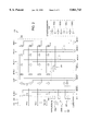
- FIG. 2 is a schematic block diagram of the hybrid scanner 112 of the present invention.
- Hybrid scanner 112 includes a matrix 202 for switching internal scanner buses to system pin channels. As will be discussed in detail below, semiconductor switches switch most scanner buses to system pin channels, but mechanical relays perform switching for at least one bus used for high-current test signals.
- Each of the scanner buses is connectable to one or more of the test instruments described above with reference to FIG. 1.
- Scanner 112 is connectable through mechanical relays (discussed below) to overdrivers 106, guard path 111, and driver/sensors 104, which in the preferred embodiment are located on one of the printed-circuit boards on which the scanner switches are mounted.
- the scanner is coupled to other analog instruments through one or more instrument buses, connected to one or more scanner buses, by mechanical relays 201.
- Matrix 202 is implemented with six scanner buses, Bus0-Bus5, preferably having a dual channel configuration.
- one channel of a scanner bus is connectable to some of the system pin channels 204 while the other channel of the same bus is connectable to some or all of the remaining system pin channels.
- this is implemented with each of the two channels of a scanner bus connectable to alternating system pin channels.
- matrix 202 is implemented with a majority of semiconductor switches which, as is well known, have an inherent capacitance which is high compared to the mechanical switches. The accumulation of this capacitance on any single scanner bus channel, which may interfere with the accuracy of test measurements, is avoided with the dual-bus structure of the preferred embodiment. By connecting one of the bus channels to a portion of the system pin channels, the bus channel is only connectable to a portion of the semiconductor switches.
- one of the six scanner buses, Bus 0 is dedicated to supporting low impedance guarding and high current backdriving test operations.
- mechanical relays 210 are used to connect both channels of Bus 0 to the system pin channels 204.
- overdrivers 106 and guard path 111 are coupled to Bus 0 with mechanical relays 205 and 207, respectively.
- one overdriver is coupled to each channel of the preferred dual channel Bus 0 by an independently controllable mechanical relay. This enables the dual-channel configuration of the matrix internal buses to provide greater flexibility in performing overdriving/backdriving operations by providing access to two adjacent system pins 203.
- Overdrivers 106 are digital drivers that momentarily force an IC input to a desired logic level regardless of what state that input is being held to by another IC.
- Overdrivers 106 preferably include two overdrivers: overdriver 205A to generate a logic high overdrive signal and overdriver 204B to generate a logic low overdrive signal.
- each overdriver 204A, 204B is coupled to both channels of Bus 0 through independently-controllable mechanical relays.
- the logic levels of overdrivers 204 are programmable in the range 0V to 5V with 8-bit resolution (approximately 25 mV).
- each overdriver 204 is configured to overdrive/backdrive one system pin at a given time.
- each overdriver 106 is capable of sinking or sourcing 500 mA, with a programmable current limit and a resolution of approximately 25 mA.
- the 500 mA capacity enables each ovedriver to backdrive more than one system pin 116.
- the overdrivers draw power from backdrive rails on the scanner backplane (not shown), which has a total current limit of 2 A to protect system power supplies. In FIG. 2 the leads to the scanner backplane are omitted for clarity.
- guard path 111 For low-impedance guarding, guard path 111 provides a ground voltage potential to either or both channels of Bus 0 by independently controllable mechanical relays 207.
- semiconductor switches 212 are DG445 CMOS switches, selected for a compromise between switch resistance and capacitance.
- CMOS switches 212 have a nominal resistance of approximately 35 ohms, but may be as high as 80 ohms. Two such switches in series will adversely affect measurement accuracy. To prevent this, it is preferable to include only one CMOS switch in a test channel. Accordingly, each of the driver/sensors 104 is connectable to a scanner bus with a mechanical relay such as mechanical relay 209.
- the driver/sensors 106 are provided for performing low-accuracy analog stimulus/measurements, and for digital sensing. Each driver can have an independently-programmable voltage level in the range 0V to 5V with 8-bit resolution (about 25mV).
- Two drivers 208A and 208C are configured to drive to high logic levels while the other two driver/sensors 208B and 208D are configured to drive to low logic levels.
- the drivers have a fixed current limit of approximately 25 mA, so each can drive up to 20 standard TTL loads, or 60 LSTTL loads, or a CMOS load with a total capacitance up to 2500 pF.
- the two pairs of drivers 208A/208B and 208C/208D can support 2 logic families (suitable for UUTs with mixed 5V/3V logic) or can be used in parallel to drive larger loads.
- the four sensors have independently-programmable reference voltages, again programmable in the range 0V to 5V with 8-bit resolution. Also, the sensors have a 100 kohm input resistance.
- FIG. 3 is a schematic block diagram of an exemplary impedance test. Review of this diagram reveals one of the considerations that gave rise to the present invention.
- Circuit 300 includes not only impedance Z x , whose value is to be measured, but also impedances Z a and Z b . This circuit may represent several situations, such as a three terminal standard capacitor where Z a and Z b represent stray capacitance at the case or guard (point C). Alternatively, the circuit may represent an impedance, Z x , included in a network where Z a and Z b represent actual circuit components shunting Z x . As another example, the circuit 300 may represent any passive three terminal network whose short circuit transfer impedance is desired.
- the hybrid scanner 112 of the present invention is used to effect a six-terminal measurement configuration.
- This is a typical measurement configuration long used by in-circuit testers.
- the instrument-to-probe connections have been made by relay-only scanners in order to minimize scanner switch resistance, the primary contributor to measurement errors. The reason for this can be appreciated by considering one error source, namely, guard lead error, which renders all-semiconductor switches unsuitable for many testing purposes, such as in low-impedance measurements.
- Guard lead error consists mainly of the product of the guard resistance and the impedance of Z x , divided by the product of Z a and Z b .
- the impedance of Z x is high as compared to Z a and Z b , then the contribution of this error term is significant.
- the illustrated hybrid scanner provides access to guard path 111 through mechanical relays, thereby reducing the guard lead error.
- guard terminal C of FIG. 3 is connected to guard path 111 through high-current, low-impedance scanner Bus 0 through relays 210 and 207.
- guard terminal C is connected to current meter 304 through scanner Bus 2 and a semiconductor switch 212. In the case of that connection, this error is acceptable because little current flows through it. But even most other higher current connections can be made by semiconductor switch, for example, as illustrated above in FIG. 3 with the use of separate sense and force connections.
- terminal A is connected to a voltage source 302 and DVM 110 through scanner Bus 1 and scanner Bus 5, respectively, through semiconductor switches 212.
- Terminal B is connected to the output of current meter 304 and DVM 110 via scanner Bus 3 and scanner Bus 4, respectively, through semiconductor switches 212.
- Terminal C is coupled to the guard sense input of the current meter through scanner Bus 2.
- the input of the current sensor 304 sense input
- the current meter resistor the force input
- the input of the current meter is connected to the DVM, and thus to node B through Bus 4 whereas the current meter input is coupled to node B through Bus 3. Since no current flows through the current meter input, it is preferably coupled to Bus 4 since there in no current flow to the DVM 110.
- the voltage source 302 has a sense input coupled to node A through Bus 5 whereas the force input is coupled to node A through Bus 1.
- the sense lines can be connected to the force lines and the voltage drop across the switch is not corrected for. Instead, the voltage drop across the nodes is measured and considered in the calculations. This configuration is particularly useful when the current through the switch is very high such as when low impedance measurements are performed.
- the hybrid scanner of the present invention is fully capable of supporting in-circuit tests covering the most significant regions of the fault spectrum with a limited number of mechanical relays. Because it supports backdriving and guarding test techniques, the scanner of the present invention can be used in a tester that identifies defects such as short circuits, open circuits, missing, incorrect, and backwards components, some bent-lead and analog-specification defects, and defects in digital logic, the sum of which account for a significant portion of the PCB fault spectrum.
- the scanner achieves this significant test-supporting capability while achieving greater reliability, reduced size, and lower cost than the scanners conventionally used in traditional broad spectrum testers.
- the novel implementation of a scanner matrix populated primarily by semiconductor switches rather than mechanical relays significantly reduces cost of the scanner, depending on the number of scanner buses dedicated to carrying low-impedance, high-current test signals.
- the significant reduction in switch size reduces the size of the supporting circuit board, thereby eliminating the need for additional mechanical structures to prevent the scanner circuit boards such as those used in all-relay scanners, from warping. Also, four semiconductor switches can fit into the scanner circuit board area of a single mechanical relay, thereby requiring fewer scanner circuit boards for a given scanner configuration as well as simplifying the mechanical packaging of the scanner.
- Another advantage is the increased reliability achieved by the hybrid scanner.
- the contact resistance of mechanical relays tends to increase with their use due to contact surfaces wear. This increased resistance eventually interferes with, and leads to, unreliable operations.
- semiconductor switches can operate for significantly longer periods of time without degradation.
- Another advantage of the hybrid scanner of the present invention is its significantly low power consumption.
- a relay coil dissipitates significant power when energized.
- a system with numerous mechanical relays requires large and often expensive power supplies, as well as associated power distribution cables.
- the use of semiconductor switches eliminates the need for such components.
- Another advantage of the present invention is the simplicity with which the scanner can be operated.
- a semiconductor switch can be driven by low-level logic signals whereas mechanical relays need to be driven by specific driver circuits for reliable operation.
- driver circuits add to the cost of the test system and consume broad space and power.
Abstract
Description
Claims (7)
Priority Applications (3)
| Application Number | Priority Date | Filing Date | Title |
|---|---|---|---|
| US08/576,008 US5861743A (en) | 1995-12-21 | 1995-12-21 | Hybrid scanner for use in an improved MDA tester |
| EP96309328A EP0780695A3 (en) | 1995-12-21 | 1996-12-18 | Hybrid scanner for use in a tester |
| JP34321096A JP4138041B2 (en) | 1995-12-21 | 1996-12-24 | Hybrid scanner for use with an improved MDA tester |
Applications Claiming Priority (1)
| Application Number | Priority Date | Filing Date | Title |
|---|---|---|---|
| US08/576,008 US5861743A (en) | 1995-12-21 | 1995-12-21 | Hybrid scanner for use in an improved MDA tester |
Publications (1)
| Publication Number | Publication Date |
|---|---|
| US5861743A true US5861743A (en) | 1999-01-19 |
Family
ID=24302605
Family Applications (1)
| Application Number | Title | Priority Date | Filing Date |
|---|---|---|---|
| US08/576,008 Expired - Lifetime US5861743A (en) | 1995-12-21 | 1995-12-21 | Hybrid scanner for use in an improved MDA tester |
Country Status (3)
| Country | Link |
|---|---|
| US (1) | US5861743A (en) |
| EP (1) | EP0780695A3 (en) |
| JP (1) | JP4138041B2 (en) |
Cited By (27)
| Publication number | Priority date | Publication date | Assignee | Title |
|---|---|---|---|---|
| US20030035416A1 (en) * | 2001-08-15 | 2003-02-20 | Srdan Zirojevic | Dynamically determining a route through one or more switch devices at program execution time |
| US20040150416A1 (en) * | 1999-06-30 | 2004-08-05 | Cowan Clarence E. | Probe station thermal chuck with shielding for capacitive current |
| US20040222807A1 (en) * | 2003-05-06 | 2004-11-11 | John Dunklee | Switched suspended conductor and connection |
| US20040232935A1 (en) * | 2003-05-23 | 2004-11-25 | Craig Stewart | Chuck for holding a device under test |
| US20050007581A1 (en) * | 2001-08-31 | 2005-01-13 | Harris Daniel L. | Optical testing device |
| US20050088191A1 (en) * | 2003-10-22 | 2005-04-28 | Lesher Timothy E. | Probe testing structure |
| US20050099192A1 (en) * | 2002-11-25 | 2005-05-12 | John Dunklee | Probe station with low inductance path |
| US20050140384A1 (en) * | 2003-12-24 | 2005-06-30 | Peter Andrews | Chuck with integrated wafer support |
| US20050184744A1 (en) * | 1992-06-11 | 2005-08-25 | Cascademicrotech, Inc. | Wafer probe station having a skirting component |
| US20050287685A1 (en) * | 2004-06-14 | 2005-12-29 | Mcfadden Bruce | Localizing a temperature of a device for testing |
| US20060028200A1 (en) * | 2000-09-05 | 2006-02-09 | Cascade Microtech, Inc. | Chuck for holding a device under test |
| US20060092505A1 (en) * | 2004-11-02 | 2006-05-04 | Umech Technologies, Co. | Optically enhanced digital imaging system |
| US20060103403A1 (en) * | 1995-04-14 | 2006-05-18 | Cascade Microtech, Inc. | System for evaluating probing networks |
| US20060132157A1 (en) * | 1992-06-11 | 2006-06-22 | Cascade Microtech, Inc. | Wafer probe station having environment control enclosure |
| US20060170441A1 (en) * | 2005-01-31 | 2006-08-03 | Cascade Microtech, Inc. | Interface for testing semiconductors |
| US20060169897A1 (en) * | 2005-01-31 | 2006-08-03 | Cascade Microtech, Inc. | Microscope system for testing semiconductors |
| US20070194778A1 (en) * | 2002-12-13 | 2007-08-23 | Cascade Microtech, Inc. | Guarded tub enclosure |
| US20080042669A1 (en) * | 2000-09-05 | 2008-02-21 | Cascade Microtech, Inc. | Probe station |
| US20080042675A1 (en) * | 2002-01-25 | 2008-02-21 | Cascade Microtech, Inc. | Probe station |
| US20080048693A1 (en) * | 1997-06-06 | 2008-02-28 | Cascade Microtech, Inc. | Probe station having multiple enclosures |
| US20080054922A1 (en) * | 2002-11-08 | 2008-03-06 | Cascade Microtech, Inc. | Probe station with low noise characteristics |
| US7656172B2 (en) | 2005-01-31 | 2010-02-02 | Cascade Microtech, Inc. | System for testing semiconductors |
| US20110078526A1 (en) * | 2006-02-22 | 2011-03-31 | Paul Mohr | Method and Circuit Configuration for Simulating Fault States in a Control Unit |
| US8319503B2 (en) | 2008-11-24 | 2012-11-27 | Cascade Microtech, Inc. | Test apparatus for measuring a characteristic of a device under test |
| US20180321317A1 (en) * | 2015-11-06 | 2018-11-08 | Divmac - Projectos, Automatismos E Perifericos Industriais, S.A | Automated test equipment and its operation method |
| US11219134B2 (en) * | 2019-01-28 | 2022-01-04 | Hefei Boe Vision-Electronic Technology Co., Ltd. | Device and method for detecting missing element on circuit board |
| EP4184186A4 (en) * | 2020-07-29 | 2024-01-24 | China Nuclear Power Operations Co Ltd | Intelligent test system and method for memory panel |
Families Citing this family (3)
| Publication number | Priority date | Publication date | Assignee | Title |
|---|---|---|---|---|
| CN107064693B (en) * | 2017-05-25 | 2023-06-16 | 贵州电网有限责任公司电力科学研究院 | Relay protection device outlet matrix test device and test method |
| CN108766089B (en) * | 2018-06-04 | 2020-10-30 | 浙江大学 | System and method for diagnosing wiring faults of electric circuit |
| CN115856588B (en) * | 2023-02-22 | 2023-08-04 | 长鑫存储技术有限公司 | Chip test board and test method |
Citations (11)
| Publication number | Priority date | Publication date | Assignee | Title |
|---|---|---|---|---|
| US3795860A (en) * | 1972-07-13 | 1974-03-05 | Teradyne Inc | Network tester employing latched test switching units |
| US3806800A (en) * | 1972-12-26 | 1974-04-23 | Ibm | Method and apparatus for determining the location of electrically conductive members on a structure |
| US3922537A (en) * | 1974-09-26 | 1975-11-25 | Instrumentation Engineering | Multiplex device for automatic test equipment |
| US4300207A (en) * | 1979-09-25 | 1981-11-10 | Grumman Aerospace Corporation | Multiple matrix switching system |
| US4390837A (en) * | 1980-08-25 | 1983-06-28 | Kevin Hotvedt | Test unit for a logic circuit analyzer |
| US4392107A (en) * | 1980-09-09 | 1983-07-05 | The Bendix Corporation | Switching equipment for testing apparatus |
| EP0143623A2 (en) * | 1983-11-25 | 1985-06-05 | Mars Incorporated | Automatic test equipment |
| EP0159907A2 (en) * | 1984-04-16 | 1985-10-30 | Mars Incorporated | Testing apparatus |
| US5124638A (en) * | 1991-02-22 | 1992-06-23 | Genrad, Inc. | Automatic circuit tester employing a three-dimensional switch-matrix layout |
| EP0494436A2 (en) * | 1991-01-11 | 1992-07-15 | ATG ELECTRONIC GmbH | Testing device |
| US5491427A (en) * | 1993-08-21 | 1996-02-13 | Hewlett-Packard Company | Probe and electrical part/circuit inspecting apparatus as well as electrical part/circuit inspecting method |
-
1995
- 1995-12-21 US US08/576,008 patent/US5861743A/en not_active Expired - Lifetime
-
1996
- 1996-12-18 EP EP96309328A patent/EP0780695A3/en not_active Withdrawn
- 1996-12-24 JP JP34321096A patent/JP4138041B2/en not_active Expired - Fee Related
Patent Citations (11)
| Publication number | Priority date | Publication date | Assignee | Title |
|---|---|---|---|---|
| US3795860A (en) * | 1972-07-13 | 1974-03-05 | Teradyne Inc | Network tester employing latched test switching units |
| US3806800A (en) * | 1972-12-26 | 1974-04-23 | Ibm | Method and apparatus for determining the location of electrically conductive members on a structure |
| US3922537A (en) * | 1974-09-26 | 1975-11-25 | Instrumentation Engineering | Multiplex device for automatic test equipment |
| US4300207A (en) * | 1979-09-25 | 1981-11-10 | Grumman Aerospace Corporation | Multiple matrix switching system |
| US4390837A (en) * | 1980-08-25 | 1983-06-28 | Kevin Hotvedt | Test unit for a logic circuit analyzer |
| US4392107A (en) * | 1980-09-09 | 1983-07-05 | The Bendix Corporation | Switching equipment for testing apparatus |
| EP0143623A2 (en) * | 1983-11-25 | 1985-06-05 | Mars Incorporated | Automatic test equipment |
| EP0159907A2 (en) * | 1984-04-16 | 1985-10-30 | Mars Incorporated | Testing apparatus |
| EP0494436A2 (en) * | 1991-01-11 | 1992-07-15 | ATG ELECTRONIC GmbH | Testing device |
| US5124638A (en) * | 1991-02-22 | 1992-06-23 | Genrad, Inc. | Automatic circuit tester employing a three-dimensional switch-matrix layout |
| US5491427A (en) * | 1993-08-21 | 1996-02-13 | Hewlett-Packard Company | Probe and electrical part/circuit inspecting apparatus as well as electrical part/circuit inspecting method |
Cited By (53)
| Publication number | Priority date | Publication date | Assignee | Title |
|---|---|---|---|---|
| US20080106290A1 (en) * | 1992-06-11 | 2008-05-08 | Cascade Microtech, Inc. | Wafer probe station having environment control enclosure |
| US20060132157A1 (en) * | 1992-06-11 | 2006-06-22 | Cascade Microtech, Inc. | Wafer probe station having environment control enclosure |
| US20050184744A1 (en) * | 1992-06-11 | 2005-08-25 | Cascademicrotech, Inc. | Wafer probe station having a skirting component |
| US20060103403A1 (en) * | 1995-04-14 | 2006-05-18 | Cascade Microtech, Inc. | System for evaluating probing networks |
| US20070109001A1 (en) * | 1995-04-14 | 2007-05-17 | Cascade Microtech, Inc. | System for evaluating probing networks |
| US20080048693A1 (en) * | 1997-06-06 | 2008-02-28 | Cascade Microtech, Inc. | Probe station having multiple enclosures |
| US20040150416A1 (en) * | 1999-06-30 | 2004-08-05 | Cowan Clarence E. | Probe station thermal chuck with shielding for capacitive current |
| US20070030021A1 (en) * | 1999-06-30 | 2007-02-08 | Cascade Microtech Inc. | Probe station thermal chuck with shielding for capacitive current |
| US7138813B2 (en) | 1999-06-30 | 2006-11-21 | Cascade Microtech, Inc. | Probe station thermal chuck with shielding for capacitive current |
| US20080042376A1 (en) * | 2000-09-05 | 2008-02-21 | Cascade Microtech, Inc. | Probe station |
| US20060028200A1 (en) * | 2000-09-05 | 2006-02-09 | Cascade Microtech, Inc. | Chuck for holding a device under test |
| US7969173B2 (en) | 2000-09-05 | 2011-06-28 | Cascade Microtech, Inc. | Chuck for holding a device under test |
| US7688062B2 (en) | 2000-09-05 | 2010-03-30 | Cascade Microtech, Inc. | Probe station |
| US20080054884A1 (en) * | 2000-09-05 | 2008-03-06 | Cascade Microtech, Inc. | Chuck for holding a device under test |
| US20080042642A1 (en) * | 2000-09-05 | 2008-02-21 | Cascade Microtech, Inc. | Chuck for holding a device under test |
| US20080042669A1 (en) * | 2000-09-05 | 2008-02-21 | Cascade Microtech, Inc. | Probe station |
| US20080042670A1 (en) * | 2000-09-05 | 2008-02-21 | Cascade Microtech, Inc. | Probe station |
| US20080042674A1 (en) * | 2000-09-05 | 2008-02-21 | John Dunklee | Chuck for holding a device under test |
| US7017138B2 (en) * | 2001-08-15 | 2006-03-21 | National Instruments Corporation | Dynamically determining a route through one or more switch devices at program execution time |
| US20030035416A1 (en) * | 2001-08-15 | 2003-02-20 | Srdan Zirojevic | Dynamically determining a route through one or more switch devices at program execution time |
| US20050007581A1 (en) * | 2001-08-31 | 2005-01-13 | Harris Daniel L. | Optical testing device |
| US20080042675A1 (en) * | 2002-01-25 | 2008-02-21 | Cascade Microtech, Inc. | Probe station |
| US20080054922A1 (en) * | 2002-11-08 | 2008-03-06 | Cascade Microtech, Inc. | Probe station with low noise characteristics |
| US20050099192A1 (en) * | 2002-11-25 | 2005-05-12 | John Dunklee | Probe station with low inductance path |
| US20070194778A1 (en) * | 2002-12-13 | 2007-08-23 | Cascade Microtech, Inc. | Guarded tub enclosure |
| US20040222807A1 (en) * | 2003-05-06 | 2004-11-11 | John Dunklee | Switched suspended conductor and connection |
| US20070205784A1 (en) * | 2003-05-06 | 2007-09-06 | Cascade Microtech, Inc. | Switched suspended conductor and connection |
| US7492172B2 (en) | 2003-05-23 | 2009-02-17 | Cascade Microtech, Inc. | Chuck for holding a device under test |
| US20040232935A1 (en) * | 2003-05-23 | 2004-11-25 | Craig Stewart | Chuck for holding a device under test |
| US7876115B2 (en) | 2003-05-23 | 2011-01-25 | Cascade Microtech, Inc. | Chuck for holding a device under test |
| US20090153167A1 (en) * | 2003-05-23 | 2009-06-18 | Craig Stewart | Chuck for holding a device under test |
| US20050088191A1 (en) * | 2003-10-22 | 2005-04-28 | Lesher Timothy E. | Probe testing structure |
| US8069491B2 (en) | 2003-10-22 | 2011-11-29 | Cascade Microtech, Inc. | Probe testing structure |
| US20080218187A1 (en) * | 2003-10-22 | 2008-09-11 | Cascade Microtech, Inc. | Probe testing structure |
| US20080157796A1 (en) * | 2003-12-24 | 2008-07-03 | Peter Andrews | Chuck with integrated wafer support |
| US20050140384A1 (en) * | 2003-12-24 | 2005-06-30 | Peter Andrews | Chuck with integrated wafer support |
| US7688091B2 (en) | 2003-12-24 | 2010-03-30 | Cascade Microtech, Inc. | Chuck with integrated wafer support |
| US20050287685A1 (en) * | 2004-06-14 | 2005-12-29 | Mcfadden Bruce | Localizing a temperature of a device for testing |
| US20060092505A1 (en) * | 2004-11-02 | 2006-05-04 | Umech Technologies, Co. | Optically enhanced digital imaging system |
| US20060169897A1 (en) * | 2005-01-31 | 2006-08-03 | Cascade Microtech, Inc. | Microscope system for testing semiconductors |
| US7656172B2 (en) | 2005-01-31 | 2010-02-02 | Cascade Microtech, Inc. | System for testing semiconductors |
| US20100097467A1 (en) * | 2005-01-31 | 2010-04-22 | Cascade Microtech, Inc. | System for testing semiconductors |
| US20060170441A1 (en) * | 2005-01-31 | 2006-08-03 | Cascade Microtech, Inc. | Interface for testing semiconductors |
| US7898281B2 (en) | 2005-01-31 | 2011-03-01 | Cascade Mircotech, Inc. | Interface for testing semiconductors |
| US20090134896A1 (en) * | 2005-01-31 | 2009-05-28 | Cascade Microtech, Inc. | Interface for testing semiconductors |
| US7940069B2 (en) | 2005-01-31 | 2011-05-10 | Cascade Microtech, Inc. | System for testing semiconductors |
| US20110078526A1 (en) * | 2006-02-22 | 2011-03-31 | Paul Mohr | Method and Circuit Configuration for Simulating Fault States in a Control Unit |
| US8589139B2 (en) * | 2006-02-22 | 2013-11-19 | Robert Bosch Gmbh | Method and circuit configuration for simulating fault states in a control unit |
| US8319503B2 (en) | 2008-11-24 | 2012-11-27 | Cascade Microtech, Inc. | Test apparatus for measuring a characteristic of a device under test |
| US20180321317A1 (en) * | 2015-11-06 | 2018-11-08 | Divmac - Projectos, Automatismos E Perifericos Industriais, S.A | Automated test equipment and its operation method |
| US10534035B2 (en) * | 2015-11-06 | 2020-01-14 | Divmac—Projectos, Automatismos E Perifericos Industrials, S.A. | Automated test equipment and its operation method |
| US11219134B2 (en) * | 2019-01-28 | 2022-01-04 | Hefei Boe Vision-Electronic Technology Co., Ltd. | Device and method for detecting missing element on circuit board |
| EP4184186A4 (en) * | 2020-07-29 | 2024-01-24 | China Nuclear Power Operations Co Ltd | Intelligent test system and method for memory panel |
Also Published As
| Publication number | Publication date |
|---|---|
| JPH09218245A (en) | 1997-08-19 |
| EP0780695A2 (en) | 1997-06-25 |
| JP4138041B2 (en) | 2008-08-20 |
| EP0780695A3 (en) | 1998-01-21 |
Similar Documents
| Publication | Publication Date | Title |
|---|---|---|
| US5861743A (en) | Hybrid scanner for use in an improved MDA tester | |
| US6677744B1 (en) | System for measuring signal path resistance for an integrated circuit tester interconnect structure | |
| US7245139B2 (en) | Tester channel to multiple IC terminals | |
| US6087843A (en) | Integrated circuit tester with test head including regulating capacitor | |
| JP3437872B2 (en) | Method and apparatus for testing integrated circuit under mixed signal | |
| US7453282B2 (en) | Input and output circuit of an integrated circuit and a method for testing the same | |
| US8872534B2 (en) | Method and apparatus for testing devices using serially controlled intelligent switches | |
| US7159159B2 (en) | Circuit and method for adding parametric test capability to digital boundary scan | |
| US6194911B1 (en) | Integrated circuit tester with compensation for leakage current | |
| KR20070097095A (en) | A method and apparatus for increasing the operating frequency of a system for testing electronic devices | |
| CN110910800A (en) | Source driver | |
| JP2008107216A (en) | Measuring method, switching device and measuring system equipped with the switching device | |
| US6429677B1 (en) | Method and apparatus for characterization of gate dielectrics | |
| US7256602B2 (en) | Electrical circuit and method for testing integrated circuits | |
| KR100906513B1 (en) | Electronic circuit and method for testing | |
| GB2149129A (en) | Automatic test equipment | |
| JPH11264853A (en) | Contact test device and semiconductor test device | |
| KR20010070252A (en) | Reference voltage setting method and apparatus for semiconductor ic tester | |
| KR100355716B1 (en) | Test method of low resistor for in-circuit tester | |
| US6411115B2 (en) | Apparatus for testing a semiconductor and process for the same | |
| JPH11304880A (en) | Semiconductor testing device | |
| JP2537030Y2 (en) | LSI tester | |
| JP2001296333A (en) | Ic tester | |
| KR20020064116A (en) | Ic test system | |
| JPH10206502A (en) | Analog boundary scanning-capable semiconductor integrated circuit device |
Legal Events
| Date | Code | Title | Description |
|---|---|---|---|
| AS | Assignment |
Owner name: GENRAD, INC., MASSACHUSETTS Free format text: ASSIGNMENT OF ASSIGNORS INTEREST;ASSIGNORS:PYE, RICHARD;KHAZAM, MOSES;REEL/FRAME:007943/0330 Effective date: 19960404 |
|
| STCF | Information on status: patent grant |
Free format text: PATENTED CASE |
|
| AS | Assignment |
Owner name: FLEET NATIONAL BANK, AS AGENT, MASSACHUSETTS Free format text: PATENT COLLATERAL ASSIGNMENT AND SECURITY AGREEMENT;ASSIGNOR:GENRAD, INC.;REEL/FRAME:010731/0078 Effective date: 20000324 |
|
| FPAY | Fee payment |
Year of fee payment: 4 |
|
| SULP | Surcharge for late payment | ||
| REMI | Maintenance fee reminder mailed | ||
| FPAY | Fee payment |
Year of fee payment: 8 |
|
| AS | Assignment |
Owner name: GENRAD, INC., MASSACHUSETTS Free format text: ASSIGNMENT OF ASSIGNORS INTEREST;ASSIGNOR:BANK OF AMERICA;REEL/FRAME:019733/0312 Effective date: 20070731 |
|
| FPAY | Fee payment |
Year of fee payment: 12 |
|
| AS | Assignment |
Owner name: BARCLAYS BANK PLC, NEW YORK Free format text: PATENT SECURITY AGREEMENT;ASSIGNORS:TERADYNE, INC.;LITEPOINT CORPORATION;REEL/FRAME:035507/0116 Effective date: 20150427 |
|
| AS | Assignment |
Owner name: LITEPOINT CORPORATION, CALIFORNIA Free format text: RELEASE OF SECURITY INTEREST IN INTELLECTUAL PROPERTY;ASSIGNOR:BARCLAYS BANK PLC, AS COLLATERAL AGENT;REEL/FRAME:049632/0940 Effective date: 20190627 Owner name: EAGLE TEST SYSTEMS, INC., ILLINOIS Free format text: RELEASE OF SECURITY INTEREST IN INTELLECTUAL PROPERTY;ASSIGNOR:BARCLAYS BANK PLC, AS COLLATERAL AGENT;REEL/FRAME:049632/0940 Effective date: 20190627 Owner name: NEXTEST SYSTEMS CORPORATION, CALIFORNIA Free format text: RELEASE OF SECURITY INTEREST IN INTELLECTUAL PROPERTY;ASSIGNOR:BARCLAYS BANK PLC, AS COLLATERAL AGENT;REEL/FRAME:049632/0940 Effective date: 20190627 Owner name: ENERGID TECHNOLOGIES CORPORATION, MASSACHUSETTS Free format text: RELEASE OF SECURITY INTEREST IN INTELLECTUAL PROPERTY;ASSIGNOR:BARCLAYS BANK PLC, AS COLLATERAL AGENT;REEL/FRAME:049632/0940 Effective date: 20190627 Owner name: GENRAD, LLC, MASSACHUSETTS Free format text: RELEASE OF SECURITY INTEREST IN INTELLECTUAL PROPERTY;ASSIGNOR:BARCLAYS BANK PLC, AS COLLATERAL AGENT;REEL/FRAME:049632/0940 Effective date: 20190627 Owner name: TERADYNE, INC., MASSACHUSETTS Free format text: RELEASE OF SECURITY INTEREST IN INTELLECTUAL PROPERTY;ASSIGNOR:BARCLAYS BANK PLC, AS COLLATERAL AGENT;REEL/FRAME:049632/0940 Effective date: 20190627 |
|
| AS | Assignment |
Owner name: TRUIST BANK, GEORGIA Free format text: SECURITY INTEREST;ASSIGNOR:TERADYNE, INC.;REEL/FRAME:052595/0632 Effective date: 20200501 |