US5859545A - Bidirectional buffer - Google Patents
Bidirectional buffer Download PDFInfo
- Publication number
- US5859545A US5859545A US08/777,000 US77700097A US5859545A US 5859545 A US5859545 A US 5859545A US 77700097 A US77700097 A US 77700097A US 5859545 A US5859545 A US 5859545A
- Authority
- US
- United States
- Prior art keywords
- buffer
- input
- output
- line
- low level
- Prior art date
- Legal status (The legal status is an assumption and is not a legal conclusion. Google has not performed a legal analysis and makes no representation as to the accuracy of the status listed.)
- Expired - Fee Related
Links
Images
Classifications
-
- H—ELECTRICITY
- H04—ELECTRIC COMMUNICATION TECHNIQUE
- H04L—TRANSMISSION OF DIGITAL INFORMATION, e.g. TELEGRAPHIC COMMUNICATION
- H04L25/00—Baseband systems
- H04L25/02—Details ; arrangements for supplying electrical power along data transmission lines
- H04L25/0264—Arrangements for coupling to transmission lines
- H04L25/028—Arrangements specific to the transmitter end
-
- H—ELECTRICITY
- H03—ELECTRONIC CIRCUITRY
- H03K—PULSE TECHNIQUE
- H03K19/00—Logic circuits, i.e. having at least two inputs acting on one output; Inverting circuits
- H03K19/0175—Coupling arrangements; Interface arrangements
- H03K19/01759—Coupling arrangements; Interface arrangements with a bidirectional operation
-
- H—ELECTRICITY
- H03—ELECTRONIC CIRCUITRY
- H03K—PULSE TECHNIQUE
- H03K19/00—Logic circuits, i.e. having at least two inputs acting on one output; Inverting circuits
- H03K19/02—Logic circuits, i.e. having at least two inputs acting on one output; Inverting circuits using specified components
- H03K19/173—Logic circuits, i.e. having at least two inputs acting on one output; Inverting circuits using specified components using elementary logic circuits as components
- H03K19/1731—Optimisation thereof
- H03K19/1732—Optimisation thereof by limitation or reduction of the pin/gate ratio
-
- H—ELECTRICITY
- H04—ELECTRIC COMMUNICATION TECHNIQUE
- H04L—TRANSMISSION OF DIGITAL INFORMATION, e.g. TELEGRAPHIC COMMUNICATION
- H04L25/00—Baseband systems
- H04L25/02—Details ; arrangements for supplying electrical power along data transmission lines
- H04L25/0264—Arrangements for coupling to transmission lines
- H04L25/0292—Arrangements specific to the receiver end
-
- H—ELECTRICITY
- H04—ELECTRIC COMMUNICATION TECHNIQUE
- H04L—TRANSMISSION OF DIGITAL INFORMATION, e.g. TELEGRAPHIC COMMUNICATION
- H04L5/00—Arrangements affording multiple use of the transmission path
- H04L5/14—Two-way operation using the same type of signal, i.e. duplex
- H04L5/16—Half-duplex systems; Simplex/duplex switching; Transmission of break signals non-automatically inverting the direction of transmission
Definitions
- This invention relates to bus line buffering and in particular to buffering for a two-way bus.
- the device may not be able to sink enough current to force the bus lines low.
- Such buffering is easy to implement if the device D has separate terminals for input and output, ie one terminal 2 for reading an open-collector bus line (external line 4) and a different terminal 3 for forcing the line low, as illustrated in FIG. 1.
- the symbol in buffer 6 denotes an open-collector output.
- the output buffer 6 must be able to distinguish between two different causes for a low level on the device side, ie on the internal line:
- the device D is pulling it low.
- the device D is not pulling it low but the input buffer 5 is.
- the present invention aims to provide a solution which does not suffer from the aforementioned disadvantages.
- a buffer circuit for use between a bus line and an input/output terminal of a device capable of reading the status of the bus line and driving it low
- the buffer circuit including a line which is connected in use to the terminal, an input buffer in parallel with an output buffer, the input of the input buffer being connected to the output of the output buffer and connected in use to the bus line, the output of the input buffer being connected to the input of the output buffer and to the line, and the buffer circuit being such that two logical levels of the same type which may be present on the line and have different sources are distinguishable from one another, characterised in that the output buffer is in the form of a comparator which compares any said logical level with a reference level and interprets it as arising from a first source if it is less that the reference level or as arising from a second source if it is greater than the reference level, and the output buffer is such as to distinguish between two logical low levels on the line, whose sources are the device or the input buffer, respectively, pulling the line low
- a method of buffering a connection between a bus line and a device capable of reading the status of the bus line and driving it low including the step of disposing a buffer circuit including an input buffer and an output buffer, between the bus line and an input/output terminal of the device, the buffer circuit being connected by a line to the terminal; and characterised in that the output buffer is in the form of a comparator, and comprising the steps of determining whether a logical low level on the line is caused by the device or the input buffer pulling it low by comparing, at the output buffer comparator, any said logical low level on the line with a reference level and interpreting it as arising from the device if it is on one side of the reference level and as arising from the input buffer if it is on the other side of the reference level; and pulling the bus line low by means of the output buffer when the device is pulling the line low.
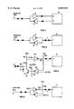
- FIG. 1 illustrates a first known buffer circuit
- FIG. 2 illustrates an impractical buffer circuit
- FIG. 3 illustrates a specific embodiment of the present invention
- FIG. 4 illustrates a more general arrangement of the embodiment of FIG. 3.
- the solution provided by the present invention does not involve the disadvantages associated with the prior art circuits and is suitable for use when there is a reasonable voltage margin between the low output level of the device D and the highest input voltage that the device D is guaranteed to interpret as low level.
- the solution distinguishes between cases A and B by comparing the two different low-level voltages on the internal line 7 with a reference.
- the line 7 will be at a high level when neither the device nor the input buffer is pulling it low.
- U a is defined as the low-level output voltage of the device D and U c is defined as the highest input voltage that the device D is guaranteed to recognise as low level.
- U b denote a voltage which is between U a and U c and is preferably closer to U c than U a .
- the input buffer is, according to the invention, designed so that its low-level output pulls down the internal line 7 to level U b when the device D is not pulling the internal line 7 low, and the output buffer is designed so that it interprets U a as low (Case A) and U b as high (Case B).
- the output buffer pulls the external (bus line) 4 low.
- the input and output buffers may be implemented by a low cost comparator, such as an LM339 comparator, with or without an extra transistor, depending upon requirements, as will be apparent from the following.
- a low cost comparator such as an LM339 comparator
- the first example, illustrated in FIG. 3, relates to an arrangement for use, for example, in a video monitor where the external line (bus) is an ACCESS bus or I 2 C bus.
- the device D consists of a local bus to which one or more integrated circuits with I 2 C ports are connected. It is assumed that all of the reasons 1, 2 and 3, as referred to above with respect to prior art arrangements, apply. If this is not the case, the implementation can be simplified.
- the I 2 C bus consists of two bus lines (a clock line and a data line) but FIG. 3 applies equally to either of them.
- the LM339 which is a low cost comparator integrated circuit with open-collector outputs, contains four comparators, two of which C1 and C2 are employed in the FIG. 3 embodiment. Thus only one LM339 is needed for the overall bus.
- the LM339 requires a +5V power supply and this may be supplied from a host PC associated with the video monitor or derived from the monitor supply itself, for example.
- the low-level output of I 2 C ports is ⁇ 0.4 volts at 3 mA sink current, so that with a 3.92K ohms load resistor R4, U a will be less than 0.4V and typically 0.2V.
- U c for I 2 C ports is 1.5V.
- the voltage divider R7/R4 (909 ohms/3.92 Kohms) will make U b nominally equal to 1.0V, which is safely below U c , and the output comparator C2 can safely distinguish between U a (Case A) and U b (Case B).
- the output transistor T1 (2N2369 or equivalent) can sink at least 20 mA.
- Reason 3 is safely taken care of if the signal BUFEN is high when the +5V power supply is stable only. The latter can be achieved by deriving BUFEN from the reset and/or power-watch circuitry that is normally present in a microprocessor system such as of a video monitor. If reason 3 is unimportant, then BUFEN can be simply replaced by a direct connection to +5V.
- Both the LM339 input (comparator C1) and the transistor T1 (2N2369) can withstand voltage transients up to +36V from the external line, whether the +5V is on or not. Negative transients are absorbed by diode D1 (1N4148), combined with the fact that the input to the LM339 will then be 0.9V more positive, because of the divider R3/R2, using the values 6.8K/39K, so that the LM339 comparator C1 never gets input levels that are negative enough to disturb proper operation.
- the reference voltages +2.4V and +0.65V may be obtained from the +5V supply by means of a three-resistor voltage divider.
- R1 is 51 ohms
- R5 is 4.7 Kohms
- R6 is 3.3 Kohms, when the values of R2, R3, R4 and R7 are as quoted above.
- FIG. 3 shows a basic implementation circuit which is sufficient if the chosen comparator integrated circuit is adequate as it is for the various requirements.
- the values of R8 and R9 can be the same as or different to the values of R4 and R7 referred to above.
Abstract
Description
Claims (10)
Applications Claiming Priority (3)
| Application Number | Priority Date | Filing Date | Title |
|---|---|---|---|
| GB9416380 | 1994-08-12 | ||
| GB9416380A GB2292277B (en) | 1994-08-12 | 1994-08-12 | Bus line buffering |
| PCT/EP1995/003178 WO1996005671A1 (en) | 1994-08-12 | 1995-08-10 | Bidirectional buffer |
Publications (1)
| Publication Number | Publication Date |
|---|---|
| US5859545A true US5859545A (en) | 1999-01-12 |
Family
ID=10759824
Family Applications (1)
| Application Number | Title | Priority Date | Filing Date |
|---|---|---|---|
| US08/777,000 Expired - Fee Related US5859545A (en) | 1994-08-12 | 1995-08-10 | Bidirectional buffer |
Country Status (6)
| Country | Link |
|---|---|
| US (1) | US5859545A (en) |
| EP (1) | EP0775399B1 (en) |
| DE (1) | DE69515315T2 (en) |
| ES (1) | ES2144138T3 (en) |
| GB (1) | GB2292277B (en) |
| WO (1) | WO1996005671A1 (en) |
Cited By (12)
| Publication number | Priority date | Publication date | Assignee | Title |
|---|---|---|---|---|
| US6078974A (en) * | 1998-04-08 | 2000-06-20 | Cybex Computer Products Corporation | Method and apparatus for extension of bi-directional open collector signals in a multiplexed data transmission system |
| US6172523B1 (en) * | 1998-09-30 | 2001-01-09 | Lucent Technologies Inc. | Apparatus and method for converting a non-logic-family signal level to a logic-family signal level |
| US6185643B1 (en) | 1997-11-15 | 2001-02-06 | Cybex Computer Products Corporation | Method and apparatus for extending the range between a computer and computer peripherals |
| US6265951B1 (en) | 1997-11-15 | 2001-07-24 | Cybex Computer Products Corporation | Method and apparatus for equalizing channel characteristics in a computer extension system |
| US6362654B1 (en) * | 2000-08-17 | 2002-03-26 | U.S. Philips Corporation | Bidirectional repeater using high and low threshold detection |
| US6664815B2 (en) * | 2000-12-08 | 2003-12-16 | Koninklijke Philips Electronics N.V. | Output driver circuit with current detection |
| US20040158675A1 (en) * | 2002-12-02 | 2004-08-12 | Elpida Memory, Inc. | Memory system and control method therefor |
| US20090153192A1 (en) * | 2007-12-17 | 2009-06-18 | Intersil Americas Inc. | Bi-directional buffer for open-drain or open-collector bus |
| US20090153193A1 (en) * | 2007-12-17 | 2009-06-18 | Intersil Americas Inc. | Bi-directional buffer with level shifting |
| US20090289693A1 (en) * | 2008-05-23 | 2009-11-26 | Intersil Americas Inc. | Bi-directional buffer and method for bi-directional buffering that reduce glitches due to feedback |
| US9183713B2 (en) | 2011-02-22 | 2015-11-10 | Kelly Research Corp. | Perimeter security system |
| CN113131920A (en) * | 2021-04-09 | 2021-07-16 | 成都芯源系统有限公司 | Fast low bias voltage bi-directional buffer |
Families Citing this family (3)
| Publication number | Priority date | Publication date | Assignee | Title |
|---|---|---|---|---|
| DE102008052403A1 (en) * | 2008-10-21 | 2010-04-22 | Continental Automotive Gmbh | circuitry |
| IT1391688B1 (en) * | 2008-10-30 | 2012-01-17 | Indesit Co Spa | ADAPTER DEVICE FOR BIDIRECTIONAL COMMUNICATION SYSTEM AND ITS RELATIVE SYSTEM |
| CN109018835A (en) * | 2018-09-05 | 2018-12-18 | 张晨光 | A kind of photo resistance belt indulges this protective device |
Citations (6)
| Publication number | Priority date | Publication date | Assignee | Title |
|---|---|---|---|---|
| EP0044397A1 (en) * | 1980-07-21 | 1982-01-27 | International Business Machines Corporation | Electronic switching circuit |
| JPS6064547A (en) * | 1983-09-19 | 1985-04-13 | Fujitsu Ltd | Two-way signal transmission system |
| US5214330A (en) * | 1991-07-30 | 1993-05-25 | Kabushiki Kaisha Toshiba | Bi-directional signal buffering circuit |
| US5248908A (en) * | 1990-10-03 | 1993-09-28 | Mitsubishi Denki Kabushiki Kaisha | 3-state bidirectional buffer and portable semiconductor storage device incorporating the same |
| US5587824A (en) * | 1991-07-26 | 1996-12-24 | Cybex Computer Products Corporation | Open collector communications link |
| US5736870A (en) * | 1995-12-28 | 1998-04-07 | Intel Corporation | Method and apparatus for bi-directional bus driver |
Family Cites Families (1)
| Publication number | Priority date | Publication date | Assignee | Title |
|---|---|---|---|---|
| JP3343947B2 (en) * | 1992-08-21 | 2002-11-11 | 井関農機株式会社 | Tractor steering angle detection device |
-
1994
- 1994-08-12 GB GB9416380A patent/GB2292277B/en not_active Expired - Fee Related
-
1995
- 1995-08-10 WO PCT/EP1995/003178 patent/WO1996005671A1/en active IP Right Grant
- 1995-08-10 ES ES95929841T patent/ES2144138T3/en not_active Expired - Lifetime
- 1995-08-10 DE DE69515315T patent/DE69515315T2/en not_active Expired - Fee Related
- 1995-08-10 EP EP95929841A patent/EP0775399B1/en not_active Expired - Lifetime
- 1995-08-10 US US08/777,000 patent/US5859545A/en not_active Expired - Fee Related
Patent Citations (6)
| Publication number | Priority date | Publication date | Assignee | Title |
|---|---|---|---|---|
| EP0044397A1 (en) * | 1980-07-21 | 1982-01-27 | International Business Machines Corporation | Electronic switching circuit |
| JPS6064547A (en) * | 1983-09-19 | 1985-04-13 | Fujitsu Ltd | Two-way signal transmission system |
| US5248908A (en) * | 1990-10-03 | 1993-09-28 | Mitsubishi Denki Kabushiki Kaisha | 3-state bidirectional buffer and portable semiconductor storage device incorporating the same |
| US5587824A (en) * | 1991-07-26 | 1996-12-24 | Cybex Computer Products Corporation | Open collector communications link |
| US5214330A (en) * | 1991-07-30 | 1993-05-25 | Kabushiki Kaisha Toshiba | Bi-directional signal buffering circuit |
| US5736870A (en) * | 1995-12-28 | 1998-04-07 | Intel Corporation | Method and apparatus for bi-directional bus driver |
Cited By (20)
| Publication number | Priority date | Publication date | Assignee | Title |
|---|---|---|---|---|
| US6185643B1 (en) | 1997-11-15 | 2001-02-06 | Cybex Computer Products Corporation | Method and apparatus for extending the range between a computer and computer peripherals |
| US6265951B1 (en) | 1997-11-15 | 2001-07-24 | Cybex Computer Products Corporation | Method and apparatus for equalizing channel characteristics in a computer extension system |
| US6078974A (en) * | 1998-04-08 | 2000-06-20 | Cybex Computer Products Corporation | Method and apparatus for extension of bi-directional open collector signals in a multiplexed data transmission system |
| US6172523B1 (en) * | 1998-09-30 | 2001-01-09 | Lucent Technologies Inc. | Apparatus and method for converting a non-logic-family signal level to a logic-family signal level |
| US6362654B1 (en) * | 2000-08-17 | 2002-03-26 | U.S. Philips Corporation | Bidirectional repeater using high and low threshold detection |
| US6522169B2 (en) * | 2000-08-17 | 2003-02-18 | Koninklijke Philips Electronics N.V. | Bidirectional repeater using high and low threshold detection |
| US6664815B2 (en) * | 2000-12-08 | 2003-12-16 | Koninklijke Philips Electronics N.V. | Output driver circuit with current detection |
| US20090164724A1 (en) * | 2002-12-02 | 2009-06-25 | Elpida Memory, Inc. | System and control method for hot swapping of memory modules configured in a ring bus |
| US20040158675A1 (en) * | 2002-12-02 | 2004-08-12 | Elpida Memory, Inc. | Memory system and control method therefor |
| US20090153192A1 (en) * | 2007-12-17 | 2009-06-18 | Intersil Americas Inc. | Bi-directional buffer for open-drain or open-collector bus |
| US20090153193A1 (en) * | 2007-12-17 | 2009-06-18 | Intersil Americas Inc. | Bi-directional buffer with level shifting |
| US7692450B2 (en) | 2007-12-17 | 2010-04-06 | Intersil Americas Inc. | Bi-directional buffer with level shifting |
| US7737727B2 (en) * | 2007-12-17 | 2010-06-15 | Intersil Americas Inc. | Bi-directional buffer for open-drain or open-collector bus |
| US20100207661A1 (en) * | 2007-12-17 | 2010-08-19 | Intersil Americas Inc. | Bi-directional buffer for open-drain or open-collector bus |
| US7852120B2 (en) | 2007-12-17 | 2010-12-14 | Intersil Americas Inc. | Bi-directional buffer for open-drain or open-collector bus |
| US20090289693A1 (en) * | 2008-05-23 | 2009-11-26 | Intersil Americas Inc. | Bi-directional buffer and method for bi-directional buffering that reduce glitches due to feedback |
| US7639045B2 (en) | 2008-05-23 | 2009-12-29 | Intersil Americas Inc. | Bi-directional buffer and method for bi-directional buffering that reduce glitches due to feedback |
| US9183713B2 (en) | 2011-02-22 | 2015-11-10 | Kelly Research Corp. | Perimeter security system |
| US9530296B2 (en) | 2011-02-22 | 2016-12-27 | Kelly Research Corp. | Graduated sensory alert for a perimeter security system |
| CN113131920A (en) * | 2021-04-09 | 2021-07-16 | 成都芯源系统有限公司 | Fast low bias voltage bi-directional buffer |
Also Published As
| Publication number | Publication date |
|---|---|
| WO1996005671A1 (en) | 1996-02-22 |
| GB9416380D0 (en) | 1994-10-05 |
| DE69515315T2 (en) | 2000-10-26 |
| EP0775399B1 (en) | 2000-03-01 |
| GB2292277B (en) | 1998-11-18 |
| EP0775399A1 (en) | 1997-05-28 |
| GB2292277A (en) | 1996-02-14 |
| ES2144138T3 (en) | 2000-06-01 |
| DE69515315D1 (en) | 2000-04-06 |
Similar Documents
| Publication | Publication Date | Title |
|---|---|---|
| US5859545A (en) | Bidirectional buffer | |
| KR100313367B1 (en) | Protection against voltage conversion and overvoltage | |
| EP0485102B1 (en) | Bus driver circuit | |
| KR100312929B1 (en) | Electronic device with overvoltage protection circuit | |
| EP0141681B1 (en) | Test input multiplexing circuit | |
| EP0716379B1 (en) | Interface voltage control apparatus and method | |
| US6879191B2 (en) | Voltage mismatch tolerant input/output buffer | |
| US8230151B2 (en) | Configurable data port for I2C or single-wire broadcast interface | |
| US20080082842A1 (en) | Power supply control circuit of subsystem and subsystem | |
| US10181852B1 (en) | Voltage translator with output slew rate control | |
| US6700407B1 (en) | Extended voltage range level shifter | |
| EP0546724B1 (en) | BiCMOS bus interface output driver compatible with a mixed voltage system environment | |
| EP1032132B1 (en) | An output buffer for a low voltage differential signaling receiver | |
| GB2075314A (en) | Signal transmission system | |
| US6853221B1 (en) | Power-up detection circuit with low current draw for dual power supply circuits | |
| JP3400294B2 (en) | Pull-up circuit and semiconductor device | |
| US5591984A (en) | Current sensing daisy-chain bypass arrangement | |
| CA1304805C (en) | Data transmission system | |
| US5819099A (en) | Voltage converting I/O driver circuit | |
| US6534806B1 (en) | System for generating a reference voltage | |
| JP4077524B2 (en) | Pad driver circuit and electronic circuit having pad driver circuit | |
| EP0585140A3 (en) | Motor drive circuit. | |
| EP0366083A2 (en) | Integrated circuit having output circuit | |
| KR101139135B1 (en) | Configurable data port for I2C or single-wire broadcast interface | |
| CN112953221A (en) | Voltage conversion device |
Legal Events
| Date | Code | Title | Description |
|---|---|---|---|
| AS | Assignment |
Owner name: INTERNATIONAL COMPUTERS LIMITED, UNITED KINGDOM Free format text: ASSIGNMENT OF ASSIGNORS INTEREST;ASSIGNOR:THOMBLAD, HANS;REEL/FRAME:008463/0395 Effective date: 19970204 |
|
| FEPP | Fee payment procedure |
Free format text: PAYOR NUMBER ASSIGNED (ORIGINAL EVENT CODE: ASPN); ENTITY STATUS OF PATENT OWNER: LARGE ENTITY |
|
| FPAY | Fee payment |
Year of fee payment: 4 |
|
| REMI | Maintenance fee reminder mailed | ||
| LAPS | Lapse for failure to pay maintenance fees | ||
| STCH | Information on status: patent discontinuation |
Free format text: PATENT EXPIRED DUE TO NONPAYMENT OF MAINTENANCE FEES UNDER 37 CFR 1.362 |
|
| FP | Lapsed due to failure to pay maintenance fee |
Effective date: 20070112 |
|
| FEPP | Fee payment procedure |
Free format text: PAYER NUMBER DE-ASSIGNED (ORIGINAL EVENT CODE: RMPN); ENTITY STATUS OF PATENT OWNER: LARGE ENTITY Free format text: PAYOR NUMBER ASSIGNED (ORIGINAL EVENT CODE: ASPN); ENTITY STATUS OF PATENT OWNER: LARGE ENTITY |