US5851900A - Method of manufacturing a shallow trench isolation for a semiconductor device - Google Patents
Method of manufacturing a shallow trench isolation for a semiconductor device Download PDFInfo
- Publication number
- US5851900A US5851900A US08/848,583 US84858397A US5851900A US 5851900 A US5851900 A US 5851900A US 84858397 A US84858397 A US 84858397A US 5851900 A US5851900 A US 5851900A
- Authority
- US
- United States
- Prior art keywords
- layer
- oxide layer
- forming
- silicon nitride
- sac
- Prior art date
- Legal status (The legal status is an assumption and is not a legal conclusion. Google has not performed a legal analysis and makes no representation as to the accuracy of the status listed.)
- Expired - Lifetime
Links
Images
Classifications
-
- H—ELECTRICITY
- H01—ELECTRIC ELEMENTS
- H01L—SEMICONDUCTOR DEVICES NOT COVERED BY CLASS H10
- H01L21/00—Processes or apparatus adapted for the manufacture or treatment of semiconductor or solid state devices or of parts thereof
- H01L21/70—Manufacture or treatment of devices consisting of a plurality of solid state components formed in or on a common substrate or of parts thereof; Manufacture of integrated circuit devices or of parts thereof
- H01L21/71—Manufacture of specific parts of devices defined in group H01L21/70
- H01L21/76—Making of isolation regions between components
- H01L21/762—Dielectric regions, e.g. EPIC dielectric isolation, LOCOS; Trench refilling techniques, SOI technology, use of channel stoppers
- H01L21/76224—Dielectric regions, e.g. EPIC dielectric isolation, LOCOS; Trench refilling techniques, SOI technology, use of channel stoppers using trench refilling with dielectric materials
Definitions
- the present invention relates to a method of isolation for integrated circuit (IC), and more specifically, to a method of forming a shallow trench isolation for a semiconductor device.
- IC integrated circuit
- LOCOS LOCal Oxidation of Silicon
- STI shallow trench isolation
- LOCOS structure The LOCOS involves the formation of Field OXides (FOX) in the nonactive regions of the substrate.
- FOX Field OXides
- conventional LOCOS isolation has a limitation. For example, the bird's beaks structure and shape causes unacceptably large encroachment of the field oxide into the device active regions. Further, the topography of the LOCOS is inadequate for submicron devices.
- Trench isolation is used primarily for isolating devices in VLSI and ULSI, and hence they can be considered as replacement for conventional LOCOS isolation. Further, shallow trench isolation is gaining popularity for quarter-micron technology. In the basic shallow trench isolation (STI) technology, shallow trenches are anisotropically etched into the silicon substrate. Next, a CVD oxide is deposited onto the substrate and is then be planarization by CMP (Chemical Mechanical Polishing) or etching back.
- CMP Chemical Mechanical Polishing
- LPD oxide Liquid Phase Deposition
- the LPD oxide is a technology for forming silicon dioxide in an aqueous solution at a temperature about 40° C. (room temperature is permissible).
- the LPD oxide can be formed by immersing a silicon substrate in supersaturated hydrofluorosilicic acid (H 2 SiF 6 ) solution with silica gel.
- H 2 SiF 6 supersaturated hydrofluorosilicic acid
- the chemical reaction for the treatment solution has been proposed by Nagayama et al. (see “A new process for silica coating", J. Electrochem. Soc., 135, 1988, pp2013).
- the reaction can be shown as H 2 SiF 6 +2H 2 O ⁇ 6HF+SiO 2 ⁇ .
- the LPD oxide can be selectively deposited against a silicon nitride film. In addition, it can be conformably formed on a substrate.
- a silicon substrate an be p type or n type silicon with ⁇ 100 >crystallographic orientation.
- a P-well and an N-well are generated by photolithography and implantation processes.
- a silicon oxide layer is then formed on the P-well and N-well to act as a pad layer.
- a silicon nitride layer is deposited on the pad layer to serve as a stop layer for subsequent chemical mechanical polishing (CMP).
- CMP chemical mechanical polishing
- a plurality of shallow trenches are formed by patterning and etching.
- An oxide layer is formed by thermal oxidation on the surfaces of the trenches and on the side wall of the silicon oxide.
- the silicon oxide layer is utilized for serving as a sacrificial oxide (SAC) layer.
- a photoresist is patterned on the on the N-well to expose the P-well.
- the SAC layer that is formed on the P-well is removed by using etching.
- a BSG layer is formed along the surface of the trenches.
- a thermal process is performed for driving boron ions to diffuse from the BSG layer into the P-well.
- a channel stop layer is formed in the P-well by the thermal process.
- the BSG layer is removed.
- the SAC layer is also removed.
- An oxide layer is formed on the surfaces of the trenches and on the silicon nitride layer.
- the oxide layer 22 that is formed on the silicon nitride layer 10 is dipped off.
- a LPD oxide layer is selectively deposited and refilled into the shallow trenches. Then, a CMP process is performed to remove a portion of the LPD oxide layer for planarization. Residual LPD oxide is remained in the trenches. Thus, the shallow trench isolations are formed. Subsequently, the silicon nitride layer and the silicon oxide layer are removed, respectively. A silicon oxide layer is formed on the substrate adjacent to the shallow trench isolations. The silicon oxide is used to act a gate oxide layer.
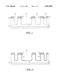
- FIG. 1 is a cross section view of a semiconductor wafer illustrating the steps of forming a P-well and a N-well in a substrate, forming a plurality of shallow trenches in the substrate in accordance with prior art;
- FIG. 2 is a cross section view of a semiconductor wafer illustrating the step of forming a SAC layer on the substrate in accordance with the present invention
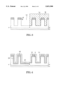
- FIG. 3 is a cross section view of a semiconductor wafer illustrating the step of removing the SAC layer that is formed on the P-well in accordance with the present invention
- FIG. 4 is a cross section view of a semiconductor wafer illustrating the steps of forming a BSG layer over the substrate and performing a thermal process to form a channel stop layer in the P-well in accordance with the present invention
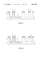
- FIG. 5 is a cross section view of a semiconductor wafer illustrating the step of removing the BSG layer in accordance with the present invention
- FIG. 6 is a cross section view of a semiconductor wafer illustrating the step of forming an oxide layer along the surface of the shallow trenches in accordance with the present invention
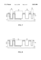
- FIG. 7 is a cross section view of a semiconductor wafer illustrating the step of forming a selective LPD-oxide in the shallow trenches for isolation in accordance with the present invention
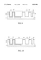
- FIG. 8 is a cross section view of a semiconductor wafer illustrating the step of performing a CMP process for planarization in accordance with the present invention
- FIG. 9 is a cross section view of a semiconductor wafer illustrating the step of removing the silicon nitride layer and the pad oxide layer in accordance with the present invention.
- FIG. 10 is a cross section view of a semiconductor wafer illustrating the step of forming a gate oxide layer on the substrate in accordance with the present invention.
- a method is disclose to create shallow trench isolations (STI) in a substrate by using LPD (Liquid Phase Deposition) oxide. Further, a BSG layer is also used for forming a channel stop in a P-well. As will be seen below, these techniques can be used for improving the planarization of the shallow trench isolations.
- LPD Liquid Phase Deposition
- a silicon substrate 2 can be p type or n type silicon with ⁇ 100 >crystallographic orientation.
- a P-well 4 and an N-well 6 are generated in a conventional manner. In other words, photolithography and ion implantation processes are used to form these two well.
- a photoresist is patterned on the N-well 6. Then, an ion implantation is used to form the P-well. The photoresist is stripped. Next, another photoresist is used to expose the P-well 6. Subsequently, the N-well is formed by ion implantation.
- a silicon oxide layer 8 is then formed on the P-well 4 and N-well 6 to act as a pad layer.
- the silicon oxide 8 is typically formed by using a thermal oxidation in an oxygen ambient.
- the silicon dioxide layer 8 is formed by using an oxygen-steam ambient, at a temperature of about 800°-1100° C.
- the oxide layer 4 may be formed using any suitable oxide chemical compositions and procedures.
- a silicon nitride layer 10 is deposited on the pad layer 8 to serve as a stop layer for subsequent chemical mechanical polishing (CMP).
- CMP chemical mechanical polishing
- the silicon nitride layer 10 can be deposited by any suitable process. For example, Low Pressure Chemical Vapor Deposition (LPCVD), Plasma Enhance Chemical Vapor Deposition (PECVD), High Density Plasma Chemical Vapor Deposition (HDPCVD).
- LPCVD Low Pressure Chemical Vapor Deposition
- PECVD Plasma Enhance Chemical Vapor Deposition
- HDPCVD High Density Plasma Chemical Vapor Deposition
- the thickness of the silicon nitride layer is about 1000 to 2000 angstroms.
- the reaction gases of the step to form silicon nitride layer 10 are SiH4, NH3, N2, N2O or SiH2Cl2, NH3, N2, N2O.
- a photoresist is patterned on the silicon nitride layer 10 to define shallow trench isolation regions. Then, an etching is used to etch the silicon nitride layer 10, the silicon oxide layer 8 and the substrate 2 by using the photoresist as an etching mask. A plurality of shallow trenches 12 are formed by this step. Typically, the depth of the shallow trenches 12 are about 2000 to 8000 angstroms from the surface of the silicon nitride layer 10. The photoresist is removed away after the trenches 12 are formed. Then, wet clean process is used to clean the substrate 2.
- an oxide layer 14 is formed by thermal oxidation on the surfaces of the trenches 12 and on the side wall of the silicon oxide 8.
- the silicon oxide layer 14 is utilized for serving as a sacrificial oxide (SAC) layer.
- the thickness of the oxide layer 14 is about 100 to 200 angstroms.
- a photoresist 16 is patterned on the on the N-well 6 to expose the P-well 4. Then, the SAC layer 14 that is formed on the P-well is removed by etching. Generally, the SAC layer 14 can be removed by using BHF solution. The photoresist 16 is then stripped away.
- a BSG layer 18 is formed along the surface of the trenches 12.
- the BSG layer 18 is formed on the substrate 2.
- the BSG layer 18 is formed on the SAC layer 14.
- a thermal process is performed in an inert ambient for driving boron ions in the BSG layer 18 to diffuse from the BSG layer 18 into the substrate 2.
- a channel stop layer 20 is formed in the P-well 4 by the thermal process.
- the SAC layer 14 on the N-well 6 can prevent the boron ions from diffusing into the N-well 6.
- the temperature of the thermal process is about 900°-1000° C.
- the BSG layer 18 is removed by using HF as the etchant.
- the SAC layer 14 is removed by using HF.
- an oxide layer 22 is formed on the surfaces of the trenches 12 and on the silicon nitride layer 10.
- the oxide layer 22 is preferably formed by thermal oxidation.
- the thickness of the oxide layer 22 is in the range of about 150 to 200 angstroms.
- the oxide layer 22 is used to provide the selective deposition of LPD oxide.
- the oxide 22 that is formed on the silicon mitride layer 10 is less than the oxide layer 22 that is in the trench 12.
- the oxide layer 22 that is formed on the silicon nitride layer 10 is then dipped off by using wet strip.
- a LPD oxide layer 24 selectively is deposited and refilled into the shallow trenches 12.
- the LPD oxide can not be formed on the silicon nitride layer 10.
- the thickness of the LPD oxide layer 14 is about 2000 to 8000 angstroms.
- the advantage of the LPD oxide layer 24 is that it can be conformably formed on a substrate 2. Further, the LPD oxide 24 is selectively deposited against the silicon nitride layer 10. Therefore, the LPD oxide layer 24 will not be formed on the silicon nitride layer 10.
- the chemical solution used to form the LPD oxide films is called "treatment solution”.
- the formation of the treatment solution according to the present invention is described as follows.
- 21 g of silica-gel powder with purity of 99.99% is added to 450 ml of industrial grade (4 mol/l) hydrofluorosilicic acid aqueous solution at the temperature of 23° C.
- the mixed solution is then stirred for 17 hours at the temperature of 23° C.
- the solution is filtered to remove the undissolved silica-gel.
- the hydrofluorosilicic acid solution saturated with silicon dioxide is obtained.
- the impurities of hydrofluorosilicic acid are listed as follows:
- the next step is the preparation of boric acid. 1.885 g of pure boric acid is added into 300 ml water. Then, the solution is stirred uniformity at 23° C. Therefore, the boric acid with concentration of 0.1 mol/l is obtained.
- 64 ml of the treatment solution (4 mol/l) is diluted with deionized water to be a concentration of 3.56 mol/l solution. Then, 5.6 ml of boric acid (0.1 mol/l) is added to the solution. The solution is uniformly stirred before the substrate is immersed into the solution. Next, the substrate is immersed into the solution at a temperature about 40° C. Thus, the LPD oxide layer 24 is formed over the substrate.
- a CMP process is performed to remove a portion of the LPD oxide layer 24 to the surface of the silicon nitride layer 10 for planarization. Residual LPD oxide 24 is remained in the trenches 12. Thus, the shallow trench isolations 24a are formed.
- the silicon nitride layer 10 and the silicon oxide layer 8 are removed, respectively.
- the silicon nitride layer 10 can be removed by hot phosphorus acid.
- the silicon oxide layer 8 is removed using HF solution.
- a further SAC layer 26 can be formed on the substrate 2 for subsequent processes. Then, the SAC layer 26 is removed.
- a silicon oxide layer 28 is formed on the substrate 2 adjacent to the shallow trench isolations 24a.
- the silicon oxide 28 is used to act a gate oxide layer 28.
Abstract
Description
______________________________________
impurity           assay
______________________________________
Fe                 0.01%
heavy metal (for example Pb)
                   0.003%
Chloride           0.005%
Sulfate(SO4)       0.01%
______________________________________
Claims (14)
Priority Applications (1)
| Application Number | Priority Date | Filing Date | Title |
|---|---|---|---|
| US08/848,583 US5851900A (en) | 1997-04-28 | 1997-04-28 | Method of manufacturing a shallow trench isolation for a semiconductor device |
Applications Claiming Priority (1)
| Application Number | Priority Date | Filing Date | Title |
|---|---|---|---|
| US08/848,583 US5851900A (en) | 1997-04-28 | 1997-04-28 | Method of manufacturing a shallow trench isolation for a semiconductor device |
Publications (1)
| Publication Number | Publication Date |
|---|---|
| US5851900A true US5851900A (en) | 1998-12-22 |
Family
ID=25303709
Family Applications (1)
| Application Number | Title | Priority Date | Filing Date |
|---|---|---|---|
| US08/848,583 Expired - Lifetime US5851900A (en) | 1997-04-28 | 1997-04-28 | Method of manufacturing a shallow trench isolation for a semiconductor device |
Country Status (1)
| Country | Link |
|---|---|
| US (1) | US5851900A (en) |
Cited By (19)
| Publication number | Priority date | Publication date | Assignee | Title |
|---|---|---|---|---|
| US5960276A (en) * | 1998-09-28 | 1999-09-28 | Taiwan Semiconductor Manufacturing Company, Ltd. | Using an extra boron implant to improve the NMOS reverse narrow width effect in shallow trench isolation process |
| US5994178A (en) * | 1997-12-31 | 1999-11-30 | Texas Instruments - Acer Incorporated | Method of fabricating CMOS transistors with a planar shallow trench isolation |
| US6069058A (en) * | 1997-05-14 | 2000-05-30 | United Semiconductor Corp. | Shallow trench isolation for semiconductor devices |
| US6133151A (en) * | 1999-05-10 | 2000-10-17 | Worldwide Semiconductor Manufacturing Corp. | HDP-CVD method for spacer formation |
| US6150235A (en) * | 2000-01-24 | 2000-11-21 | Worldwide Semiconductor Manufacturing Corp. | Method of forming shallow trench isolation structures |
| US6255190B1 (en) * | 1997-06-19 | 2001-07-03 | Austria Mikro Systeme International Ag | Method for dielectrically isolated deep pn-junctions in silicon substrates using deep trench sidewall predeposition technology |
| US20010012664A1 (en) * | 1999-09-01 | 2001-08-09 | Tran Luan C. | Semiconductor processing methods of forming transistors, semiconductor processing methods of forming dynamic random access memory circuitry, and related integrated circuitry |
| US6486517B2 (en) * | 2000-12-01 | 2002-11-26 | Samsung Electronics Co., Ltd. | Semiconductor device having shallow trench isolation structure and manufacturing method thereof |
| US20030098492A1 (en) * | 2001-11-29 | 2003-05-29 | Singh Rana P. | Semiconductor device structure and method for forming |
| US6599813B2 (en) | 2001-06-29 | 2003-07-29 | International Business Machines Corporation | Method of forming shallow trench isolation for thin silicon-on-insulator substrates |
| US6617224B2 (en) | 2000-11-03 | 2003-09-09 | Applied Materials, Inc. | Multiple stage deposition process for filling trenches |
| US20040029402A1 (en) * | 2000-08-31 | 2004-02-12 | William Budge | Use of linear injectors to deposit uniform selective ozone TEOS oxide film by pulsing reactants on and off |
| US20050035418A1 (en) * | 2000-08-31 | 2005-02-17 | Micron Technology, Inc. | Selectively deposited silicon oxide layers on a silicon substrate |
| US6888212B2 (en) * | 1997-08-22 | 2005-05-03 | Micron Technology, Inc. | Method for trench isolation by selective deposition of low temperature oxide films |
| US20050130387A1 (en) * | 2003-12-11 | 2005-06-16 | International Business Machines Corporation | Shallow trench isolation fill by liquid phase deposition of SiO2 |
| US20050215013A1 (en) * | 1999-05-25 | 2005-09-29 | Advanced Analogic Technologies, Inc. | Trench semiconductor device having gate oxide layer with mulitiple thicknesses and processes of fabricating the same |
| US20080040696A1 (en) * | 2003-12-11 | 2008-02-14 | International Business Machines Corporation | Design Structures Incorporating Shallow Trench Isolation Filled by Liquid Phase Deposition of SiO2 |
| US10910223B2 (en) | 2016-07-29 | 2021-02-02 | Taiwan Semiconductor Manufacturing Company, Ltd. | Doping through diffusion and epitaxy profile shaping |
| US11101165B2 (en) * | 2017-12-29 | 2021-08-24 | United Microelectronics Corp. | Method for fabricating semiconductor device comprising a deep trench isolation structure and a trap rich isolation structure in a substrate |
Citations (6)
| Publication number | Priority date | Publication date | Assignee | Title |
|---|---|---|---|---|
| US4666557A (en) * | 1984-12-10 | 1987-05-19 | Ncr Corporation | Method for forming channel stops in vertical semiconductor surfaces |
| US4745081A (en) * | 1985-10-31 | 1988-05-17 | International Business Machines Corporation | Method of trench filling |
| US4782036A (en) * | 1986-08-29 | 1988-11-01 | Siemens Aktiengesellschaft | Process for producing a predetermined doping in side walls and bases of trenches etched into semiconductor substrates |
| US5478776A (en) * | 1993-12-27 | 1995-12-26 | At&T Corp. | Process for fabricating integrated circuit containing shallow junction using dopant source containing organic polymer or ammonium silicate |
| US5482883A (en) * | 1993-12-01 | 1996-01-09 | International Business Machines Corporation | Method for fabricating low leakage substrate plate trench DRAM cells and devices formed thereby |
| US5726094A (en) * | 1994-02-15 | 1998-03-10 | Siemens Aktiengesellschaft | Process for producing a diffusion region adjacent to a recess in a substrate |
-
1997
- 1997-04-28 US US08/848,583 patent/US5851900A/en not_active Expired - Lifetime
Patent Citations (6)
| Publication number | Priority date | Publication date | Assignee | Title |
|---|---|---|---|---|
| US4666557A (en) * | 1984-12-10 | 1987-05-19 | Ncr Corporation | Method for forming channel stops in vertical semiconductor surfaces |
| US4745081A (en) * | 1985-10-31 | 1988-05-17 | International Business Machines Corporation | Method of trench filling |
| US4782036A (en) * | 1986-08-29 | 1988-11-01 | Siemens Aktiengesellschaft | Process for producing a predetermined doping in side walls and bases of trenches etched into semiconductor substrates |
| US5482883A (en) * | 1993-12-01 | 1996-01-09 | International Business Machines Corporation | Method for fabricating low leakage substrate plate trench DRAM cells and devices formed thereby |
| US5478776A (en) * | 1993-12-27 | 1995-12-26 | At&T Corp. | Process for fabricating integrated circuit containing shallow junction using dopant source containing organic polymer or ammonium silicate |
| US5726094A (en) * | 1994-02-15 | 1998-03-10 | Siemens Aktiengesellschaft | Process for producing a diffusion region adjacent to a recess in a substrate |
Non-Patent Citations (8)
| Title |
|---|
| K. Awaza, "Growth mechanisms of silica glasses using the liquid phase deposition (LPD)", J. Non-Cryst. Solids, 151, 1992, pp. 102-108. |
| K. Awaza, Growth mechanisms of silica glasses using the liquid phase deposition (LPD) , J. Non Cryst. Solids, 151, 1992, pp. 102 108. * |
| Nagayama et al., "A New Process for Silica Coating", J. Electrochem. Soc., 135, 1988, pp. 2013-2016. |
| Nagayama et al., A New Process for Silica Coating , J. Electrochem. Soc., 135, 1988, pp. 2013 2016. * |
| T. Goda, et al., "Physical and Chemical Properties of Silicon Dioxide Film Deposited by New Process", Mat. Res. Soc., Symp., 105, 1988, pp. 283-288. |
| T. Goda, et al., Physical and Chemical Properties of Silicon Dioxide Film Deposited by New Process , Mat. Res. Soc., Symp., 105, 1988, pp. 283 288. * |
| Wolf, S., "Silicon Processing for the VLSI Era: vol. 3, The Submicron Mosfet", Lattice Press, pp. 406-412, 1995. |
| Wolf, S., Silicon Processing for the VLSI Era: vol. 3, The Submicron Mosfet , Lattice Press, pp. 406 412, 1995. * |
Cited By (44)
| Publication number | Priority date | Publication date | Assignee | Title |
|---|---|---|---|---|
| US6069058A (en) * | 1997-05-14 | 2000-05-30 | United Semiconductor Corp. | Shallow trench isolation for semiconductor devices |
| US6255190B1 (en) * | 1997-06-19 | 2001-07-03 | Austria Mikro Systeme International Ag | Method for dielectrically isolated deep pn-junctions in silicon substrates using deep trench sidewall predeposition technology |
| US6888212B2 (en) * | 1997-08-22 | 2005-05-03 | Micron Technology, Inc. | Method for trench isolation by selective deposition of low temperature oxide films |
| US5994178A (en) * | 1997-12-31 | 1999-11-30 | Texas Instruments - Acer Incorporated | Method of fabricating CMOS transistors with a planar shallow trench isolation |
| US5960276A (en) * | 1998-09-28 | 1999-09-28 | Taiwan Semiconductor Manufacturing Company, Ltd. | Using an extra boron implant to improve the NMOS reverse narrow width effect in shallow trench isolation process |
| US6133151A (en) * | 1999-05-10 | 2000-10-17 | Worldwide Semiconductor Manufacturing Corp. | HDP-CVD method for spacer formation |
| US7238568B2 (en) * | 1999-05-25 | 2007-07-03 | Advanced Analogic Technologies, Inc. | Trench semiconductor device having gate oxide layer with multiple thicknesses and processes of fabricating the same |
| US20050215012A1 (en) * | 1999-05-25 | 2005-09-29 | Advanced Analogic Technologies, Inc. | Trench semiconductor device having gate oxide layer with multiple thicknesses and processes of fabricating the same |
| US20050215027A1 (en) * | 1999-05-25 | 2005-09-29 | Advanced Analogic Technologies, Inc. | Trench semiconductor device having gate oxide layer with multiple thicknesses and processes of fabricating the same |
| US20050215013A1 (en) * | 1999-05-25 | 2005-09-29 | Advanced Analogic Technologies, Inc. | Trench semiconductor device having gate oxide layer with mulitiple thicknesses and processes of fabricating the same |
| US7282412B2 (en) | 1999-05-25 | 2007-10-16 | Advanced Analogic Technologies, Inc. | Trench semiconductor device having gate oxide layer with multiple thicknesses and processes of fabricating the same |
| US7276411B2 (en) | 1999-05-25 | 2007-10-02 | Advanced Analogic Technologies, Inc. | Trench semiconductor device having gate oxide layer with multiple thicknesses and processes of fabricating the same |
| US7253047B2 (en) | 1999-09-01 | 2007-08-07 | Micron Technology, Inc. | Semiconductor processing methods of forming transistors, semiconductor processing methods of forming dynamic random access memory circuitry, and related integrated circuitry |
| US20060008977A1 (en) * | 1999-09-01 | 2006-01-12 | Tran Luan C | Semiconductor processing methods of forming transistors, semiconductor processing methods of forming dynamic random access memory circuitry, and related integrated circuitry |
| US7291880B2 (en) | 1999-09-01 | 2007-11-06 | Micron Technology, Inc. | Transistor assembly |
| US7057257B2 (en) | 1999-09-01 | 2006-06-06 | Micron Technology, Inc. | Semiconductor processing methods of forming transistors, semiconductor processing methods of forming dynamic random access memory circuitry, and related integrated circuitry |
| US20030020106A1 (en) * | 1999-09-01 | 2003-01-30 | Luan C. Tran | Semiconductor processing methods of forming transistors, semiconductor processing methods of forming dynamic random access memory circuitry, and related integrated circuitry |
| US20020195670A1 (en) * | 1999-09-01 | 2002-12-26 | Tran Luan C. | Semiconductor processing methods of forming transistors, semiconductor processing methods of forming dynamic random access memory circuitry, and related integrated circuitry |
| US7294903B2 (en) | 1999-09-01 | 2007-11-13 | Micron Technology, Inc. | Transistor assemblies |
| US6914287B2 (en) | 1999-09-01 | 2005-07-05 | Micron Technology, Inc | Semiconductor processing methods of forming transistors, semiconductor processing methods of forming dynamic random access memory circuitry, and related integrated circuitry |
| US20020072199A1 (en) * | 1999-09-01 | 2002-06-13 | Tran Luan C. | Semiconductor processing methods of forming transistors, semiconductor processing methods of forming dynamic random access memory circuitry, and related integrated circuitry |
| US20010012664A1 (en) * | 1999-09-01 | 2001-08-09 | Tran Luan C. | Semiconductor processing methods of forming transistors, semiconductor processing methods of forming dynamic random access memory circuitry, and related integrated circuitry |
| US20050287733A1 (en) * | 1999-09-01 | 2005-12-29 | Tran Luan C | Semiconductor processing methods of forming transistors, semiconductor processing methods of forming dynamic random access memory circuitry, and related integrated circuitry |
| US6150235A (en) * | 2000-01-24 | 2000-11-21 | Worldwide Semiconductor Manufacturing Corp. | Method of forming shallow trench isolation structures |
| US20050035418A1 (en) * | 2000-08-31 | 2005-02-17 | Micron Technology, Inc. | Selectively deposited silicon oxide layers on a silicon substrate |
| US20040029402A1 (en) * | 2000-08-31 | 2004-02-12 | William Budge | Use of linear injectors to deposit uniform selective ozone TEOS oxide film by pulsing reactants on and off |
| US7192893B2 (en) | 2000-08-31 | 2007-03-20 | Micron Technology Inc. | Use of linear injectors to deposit uniform selective ozone TEOS oxide film by pulsing reactants on and off |
| US7214979B2 (en) * | 2000-08-31 | 2007-05-08 | Micron Technology, Inc. | Selectively deposited silicon oxide layers on a silicon substrate |
| US6617224B2 (en) | 2000-11-03 | 2003-09-09 | Applied Materials, Inc. | Multiple stage deposition process for filling trenches |
| US6656783B2 (en) | 2000-12-01 | 2003-12-02 | Samsung Electronics Co., Ltd. | Semiconductor device having shallow trench isolation structure and manufacturing method thereof |
| US6486517B2 (en) * | 2000-12-01 | 2002-11-26 | Samsung Electronics Co., Ltd. | Semiconductor device having shallow trench isolation structure and manufacturing method thereof |
| US6599813B2 (en) | 2001-06-29 | 2003-07-29 | International Business Machines Corporation | Method of forming shallow trench isolation for thin silicon-on-insulator substrates |
| US20030098492A1 (en) * | 2001-11-29 | 2003-05-29 | Singh Rana P. | Semiconductor device structure and method for forming |
| US7208390B2 (en) * | 2001-11-29 | 2007-04-24 | Freescale Semiconductor, Inc. | Semiconductor device structure and method for forming |
| US20070228510A1 (en) * | 2003-12-11 | 2007-10-04 | International Business Machines Corporation | SHALLOW TRENCH ISOLATION FILL BY LIQUID PHASE DEPOSITION OF SiO2 |
| US7273794B2 (en) * | 2003-12-11 | 2007-09-25 | International Business Machines Corporation | Shallow trench isolation fill by liquid phase deposition of SiO2 |
| US20050130387A1 (en) * | 2003-12-11 | 2005-06-16 | International Business Machines Corporation | Shallow trench isolation fill by liquid phase deposition of SiO2 |
| US20080040696A1 (en) * | 2003-12-11 | 2008-02-14 | International Business Machines Corporation | Design Structures Incorporating Shallow Trench Isolation Filled by Liquid Phase Deposition of SiO2 |
| US20080197448A1 (en) * | 2003-12-11 | 2008-08-21 | International Business Machines Corporation | SHALLOW TRENCH ISOLATION FILL BY LIQUID PHASE DEPOSITION OF SiO2 |
| US7525156B2 (en) | 2003-12-11 | 2009-04-28 | International Business Machines Corporation | Shallow trench isolation fill by liquid phase deposition of SiO2 |
| US10910223B2 (en) | 2016-07-29 | 2021-02-02 | Taiwan Semiconductor Manufacturing Company, Ltd. | Doping through diffusion and epitaxy profile shaping |
| US11171003B2 (en) * | 2016-07-29 | 2021-11-09 | Taiwan Semiconductor Manufacturing Company, Ltd. | Doping through diffusion and epitaxy profile shaping |
| US11101165B2 (en) * | 2017-12-29 | 2021-08-24 | United Microelectronics Corp. | Method for fabricating semiconductor device comprising a deep trench isolation structure and a trap rich isolation structure in a substrate |
| US11521891B2 (en) | 2017-12-29 | 2022-12-06 | United Microelectronics Corp. | Semiconductor device comprising a deep trench isolation structure and a trap rich isolation structure in a substrate and a method of making the same |
Similar Documents
| Publication | Publication Date | Title |
|---|---|---|
| US5851900A (en) | Method of manufacturing a shallow trench isolation for a semiconductor device | |
| US5786262A (en) | Self-planarized gapfilling for shallow trench isolation | |
| KR100316221B1 (en) | Novel shallow trench isolation technique | |
| US7288814B2 (en) | Selective post-doping of gate structures by means of selective oxide growth | |
| KR100384761B1 (en) | N2o nitrided-oxide trench side walls and method of making isolation structure | |
| US5926722A (en) | Planarization of shallow trench isolation by differential etchback and chemical mechanical polishing | |
| US5930644A (en) | Method of forming a shallow trench isolation using oxide slope etching | |
| US6057210A (en) | Method of making a shallow trench isolation for ULSI formation via in-direct CMP process | |
| US5811345A (en) | Planarization of shallow- trench- isolation without chemical mechanical polishing | |
| US6015757A (en) | Method of oxide etching with high selectivity to silicon nitride by using polysilicon layer | |
| US6127244A (en) | Method of manufacturing semiconductor device | |
| US6331472B1 (en) | Method for forming shallow trench isolation | |
| US6599813B2 (en) | Method of forming shallow trench isolation for thin silicon-on-insulator substrates | |
| US5525535A (en) | Method for making doped well and field regions on semiconductor substrates for field effect transistors using liquid phase deposition of oxides | |
| US6987064B2 (en) | Method and composition to improve a nitride/oxide wet etching selectivity | |
| US6001704A (en) | Method of fabricating a shallow trench isolation by using oxide/oxynitride layers | |
| US5773335A (en) | Method for forming twin-tub wells in substrate | |
| US20020072196A1 (en) | Shallow trench isolation for thin silicon/silicon-on-insulator substrates by utilizing polysilicon | |
| US20040038493A1 (en) | Method for forming a trench isolation structure | |
| US6013559A (en) | Method of forming trench isolation | |
| KR100494117B1 (en) | The method for forming shallow trench isolation in semiconductor device | |
| KR100895825B1 (en) | Method for forming isolation layer in semiconductor device | |
| US20030181014A1 (en) | Method of manufacturing semiconductor device with STI | |
| KR100499630B1 (en) | Fabricating method of semiconductor device | |
| US7501326B2 (en) | Method for forming isolation layer of semiconductor device |
Legal Events
| Date | Code | Title | Description |
|---|---|---|---|
| AS | Assignment |
Owner name: MOSEL VITELIC INC., TAIWAN Free format text: ASSIGNMENT OF ASSIGNORS INTEREST;ASSIGNORS:CHU, CHIH-HSUN;YANG, CHING-NAN;REEL/FRAME:008520/0761 Effective date: 19970425 |
|
| STCF | Information on status: patent grant |
Free format text: PATENTED CASE |
|
| FEPP | Fee payment procedure |
Free format text: PAYOR NUMBER ASSIGNED (ORIGINAL EVENT CODE: ASPN); ENTITY STATUS OF PATENT OWNER: LARGE ENTITY Free format text: PAYER NUMBER DE-ASSIGNED (ORIGINAL EVENT CODE: RMPN); ENTITY STATUS OF PATENT OWNER: LARGE ENTITY |
|
| FPAY | Fee payment |
Year of fee payment: 4 |
|
| AS | Assignment |
Owner name: PROMOS TECHNOLOGIES INC., TAIWAN Free format text: ASSIGNMENT OF ASSIGNORS INTEREST;ASSIGNOR:MOSEL VITELIC, INC.;REEL/FRAME:015334/0772 Effective date: 20040427 |
|
| FPAY | Fee payment |
Year of fee payment: 8 |
|
| REMI | Maintenance fee reminder mailed | ||
| FPAY | Fee payment |
Year of fee payment: 12 |
|
| SULP | Surcharge for late payment |
Year of fee payment: 11 |
|
| FEPP | Fee payment procedure |
Free format text: PAYOR NUMBER ASSIGNED (ORIGINAL EVENT CODE: ASPN); ENTITY STATUS OF PATENT OWNER: LARGE ENTITY Free format text: PAYER NUMBER DE-ASSIGNED (ORIGINAL EVENT CODE: RMPN); ENTITY STATUS OF PATENT OWNER: LARGE ENTITY |
|
| AS | Assignment |
Owner name: CHANG LIAO HOLDINGS, LLC, DELAWARE Free format text: ASSIGNMENT OF ASSIGNORS INTEREST;ASSIGNOR:PROMOS TECHNOLOGIES INC.;REEL/FRAME:026795/0164 Effective date: 20110804 |
|
| AS | Assignment |
Owner name: HANGER SOLUTIONS, LLC, GEORGIA Free format text: ASSIGNMENT OF ASSIGNORS INTEREST;ASSIGNOR:INTELLECTUAL VENTURES ASSETS 158 LLC;REEL/FRAME:051486/0425 Effective date: 20191206 |
|
| AS | Assignment |
Owner name: INTELLECTUAL VENTURES ASSETS 158 LLC, DELAWARE Free format text: ASSIGNMENT OF ASSIGNORS INTEREST;ASSIGNOR:CHANG LIAO HOLDINGS, LLC;REEL/FRAME:051753/0925 Effective date: 20191126 Owner name: INTELLECTUAL VENTURES ASSETS 158 LLC, DELAWARE Free format text: ASSIGNMENT OF ASSIGNORS INTEREST;ASSIGNOR:CHANG LIAO HOLDINGS, LLC;REEL/FRAME:051754/0709 Effective date: 20191126 |