US5841863A - Method and apparatus for scrambling and descrambling of video signals with edge fill - Google Patents
Method and apparatus for scrambling and descrambling of video signals with edge fill Download PDFInfo
- Publication number
- US5841863A US5841863A US08/401,015 US40101595A US5841863A US 5841863 A US5841863 A US 5841863A US 40101595 A US40101595 A US 40101595A US 5841863 A US5841863 A US 5841863A
- Authority
- US
- United States
- Prior art keywords
- video
- line
- signal
- sync
- horizontal
- Prior art date
- Legal status (The legal status is an assumption and is not a legal conclusion. Google has not performed a legal analysis and makes no representation as to the accuracy of the status listed.)
- Expired - Lifetime
Links
Images


Classifications
-
- H—ELECTRICITY
- H04—ELECTRIC COMMUNICATION TECHNIQUE
- H04N—PICTORIAL COMMUNICATION, e.g. TELEVISION
- H04N7/00—Television systems
- H04N7/16—Analogue secrecy systems; Analogue subscription systems
- H04N7/167—Systems rendering the television signal unintelligible and subsequently intelligible
-
- H—ELECTRICITY
- H04—ELECTRIC COMMUNICATION TECHNIQUE
- H04N—PICTORIAL COMMUNICATION, e.g. TELEVISION
- H04N7/00—Television systems
- H04N7/16—Analogue secrecy systems; Analogue subscription systems
- H04N7/167—Systems rendering the television signal unintelligible and subsequently intelligible
- H04N7/169—Systems operating in the time domain of the television signal
- H04N7/1696—Systems operating in the time domain of the television signal by changing or reversing the order of active picture signal portions
-
- H—ELECTRICITY
- H04—ELECTRIC COMMUNICATION TECHNIQUE
- H04N—PICTORIAL COMMUNICATION, e.g. TELEVISION
- H04N7/00—Television systems
- H04N7/16—Analogue secrecy systems; Analogue subscription systems
- H04N7/167—Systems rendering the television signal unintelligible and subsequently intelligible
- H04N7/169—Systems operating in the time domain of the television signal
- H04N7/1693—Systems operating in the time domain of the television signal by displacing synchronisation signals relative to active picture signals or vice versa
Definitions
- This invention relates to signal processing of time domain electronic signals, such as video information signals.
- the invention relates to improvements in scrambling and descrambling such signals to prevent unauthorized use thereof, including several improvements in security and concealment.
- portions of the trailing edge of the active video in the preceding line and portions of the leading edge of the active video in the current line are discarded.
- the original line timing and colorburst signals are discarded and new signals are generated which are time displaced from the active video portion by the original amount before encryption.
- the type of time shifting performed may comprise any one of a number of slowly varying functions, such as a sinusoidal waveform or a linearly changing ramp signal.
- the rate of change in the signal i.e. the "wobble" is relatively slow when compared to the line rate of the input signals to be processed.
- a sinusoidal waveform having a frequency of no more than about 20 Hz is used.
- the absolute amount of time shifting performed is preferably limited to a maximum value which, in the case of NTSC video signals, does not exceed a total of 4 microseconds (plus or minus 2 microseconds in each direction).
- the instantaneous value of the time shifting waveform function at the beginning of each field is conveyed along with the field information, typically during the vertical blanking interval.
- the starting amplitude of the waveform during a given field is transmitted during the vertical blanking interval as a single byte of information which, when combined with a separately provided authorization key, enables a descrambling circuit to synthesize the scrambling waveform function.
- Decryption is the inverse of the encryption process and is performed by restoring the original timing relationship between the horizontal sync (and colorburst) and the active video portion of the corresponding line.
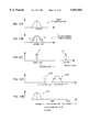
- FIGS. 1A and 1B herein correspond to FIGS. 3A and 3B of the above cited U.S. Pat. No. 5,058,157, and illustrate the manner in which the scrambled signals are descrambled at the reception site, i.e. the descrambler.
- FIG. 1A three successive lines of NTSC video are shown which have been time shifted successively by increasing amounts. (The active video portions of each of the lines in FIGS. 1A and 1B are only fractionally illustrated.)
- the topmost line represents a line N having no time shifting between the active video portion and the end of horizontal blanking, and the time between the beginning of a horizontal sync portion and the active portion is designated as t 1 .
- the precise timing relationship t 1 between the leading edge of horizontal sync and the beginning of active video ensures that each line of information, as processed by the follow-on television receiver or monitor, can be properly displayed, provided that the timing error in a given line does not exceed the capture range of the television receiver or monitor synchronization circuitry.
- the time shifting applied to the original signals during encryption is relatively slowly varying (20 Hz for NTSC TV) compared to the video line rate.
- FIGS. 2A and 2B herein are the same as FIGS. 4A and 4B of U.S. Pat. No. 5,058,157. These figures show in block diagram form a scrambler system capable of providing the above-described scrambling.
- input video to be scrambled is coupled to an input terminal 11 of a video input processor unit 12.
- Processor 12 functions to normalize the incoming video signal relative to gain, DC offset and bandwidth and provides a stable low impedance buffer unit for the video appearing on output terminal 13.
- the incoming vertical and horizontal sync portions are separated from the input video by processor unit 12 and supplied as input to a sync/timing generator and phase locked loop 15.
- the signals from processor unit 12 appearing on output terminal 13 are coupled to a conventional NTSC decoder and anti-alias filter 16 in which the luminance component Y and chrominance quadrature components I,Q are separated for three channel parallel processing in the digital domain.
- the Y output of unit 16 is coupled to an analog-to-digital converter 18 in which the luminance is converted from analog to digital form at a preselected clock rate by means of an input sample clock signal supplied on clock input line 19.
- the input of converter 18 is coupled to an input portion of a dual-ported luminance memory unit 20. This is then the Y channel memory connected to the Y channel D/A converter 22.
- Memory unit 20 is configured as a memory in which a word is written from A/D converter 18 into every memory cycle and a word is read from memory unit 20 to a digital-to-analog converter unit 22 every memory cycle.
- Read/write control signals and multi-bit address signals are supplied to the luminance memory unit 20 from a memory controller unit 24.
- the output of luminance channel memory unit 20 is coupled to the input of a digital-to-analog converter 22, in which the multi-bit digital words output from memory 20 are converted into analog samples at the clock rate by clock signals supplied from unit 15 on clock input line 23.
- the output of converter unit 22 is coupled to the input of an NTSC encoder and low pass filter unit 25 in which the luminance signal is combined with the I and Q chrominance components and renormalized with respect to band-width and DC offset.
- the I, Q chrominance quadrature components are processed in an essentially identical manner to that described above for the luminance component Y in respectively units 18', 20' and 22' and 18", 20", and 22", which function in the same manner respectively as do units 18, 20 and 22.
- Sync timing unit 15 generates the input clock signals used to provide the sample clock for A/D converter unit 18, the read and write clock signals from memory unit 20, and the clock signals for D/A converter unit 22.
- unit 15 is comprised of a discrete phase detector, a number of sampling gates, and error amplifier and a crystal clock oscillator.
- controller unit 34 is coupled to controller unit 34 and a plurality of control registers 36.
- the device is relatively expensive and complicated in that there are three sets of A/D converters and associated memories, one for each of the Y, I, and Q components.
- the method of scrambling as depicted in FIGS. 1A and 1B while reasonably secure has the potential defect that in the process of moving the active portion of the video to the right as shown in the drawings, the leading and trailing edges of the horizontal sync signal have both been moved to the right also.
- This displacement of the normally well known position of horizontal sync within the horizontal blanking interval could be detected by a clever pirate, i.e. unauthorized user, to determine the amount of wobble (time displacement) in each line.
- the pirate would be able at least in theory to descramble the signal to determine what the amount of wobble and reverse the process, thus obtaining a descrambled and viewable signal.
- the method as depicted in FIGS. 1A and 1B is lacking in the very high degree of security desirable for a commercial scrambling system.
- Another shortcoming of the above-described scrambling system is that while providing security, i.e. generally preventing unauthorized use, the scrambled signal when viewed on a normal television set is not completely concealed. That is, a determined viewer who is willing to watch a television picture which is in effect horizontally jumping back and forth can still watch the program and understand at least partly what is going on. This is undesirable for transmission for instance of adult type material where it is desired to prevent children from watching even the scrambled picture. This is especially problematic because it has been determined by experimentation that such adult type material, i.e. depictions of sexual activity, is particularly easy to follow on the picture by a viewer even though the picture is scrambled. This is another way of saying that the scrambling while relatively secure does not provide an adequate level of concealment for all program material.
- Another problem associated with the above described device is one common to comb-type NTSC decoders in which the composite video is subjected to a one-line delay. Simple addition of the delayed video to the same video before the delay causes the chrominance portion of the two signals to cancel, leaving only luminance. Similarly and simultaneously, subtraction of the delayed signal from the undelayed signal (or vice versa) causes the luminance portion to cancel, leaving only chrominance.
- This problem is not specific to a scrambling device but is typically encountered in video processors which perform NTSC decoding and is the reduction of vertical detail, resulting in smeared vertical edges in the picture.
- the luminance signal is isolated by subtracting the finished, high frequency chrominance signal from the incoming composite video so there is no loss of vertical detail.
- This process is effective but when done digitally requires two A/D conversions: one for the band passed (or high passed) chrominance and one for the broad band composite video. It would be desirable to eliminate or simplify this process in order to reduce the number of components needed and reduce the amount of processing on the signal.
- the problem of the easily detected edge of horizontal blanking in the scrambled signal is overcome by filling in the gap between the position where active video would nominally start or end and where it actually starts and ends due to the scrambling process of FIG. 1A.
- This gap is filled with signals which are undetectable compared to the expected active video, preventing the pirate from building a device which would be able to track electronically the transition at the gap.
- This "edge fill" process recognizes that for four adjacent (successive) pixels, the luminance will generally be relatively static and the chrominance will describe one complete cycle in these four pixels. Thus if at the edge of the active portion of the video, i.e.
- a low level and low frequency noise signal is added, i.e. a random noise overlay, so as to slightly disturb the steady state which is the repeated pixel data.
- This insertion of what amounts to edges, i.e. variation, in that portion of the active video would prevent the pirate from distinguishing the edge fill from the active picture by observing where there is no change.
- This random noise is provided on luminance and also both portions of the chrominance (for Y, I and Q). Otherwise, an extremely clever pirate could decode all three signals and look for a steady state on any one of them.
- This random noise is provided in either the digital or analog domain in various embodiments of the invention.
- the problem of the relative complexity of the three channel NTSC digital decoder as described above and shown in FIGS. 2A and 2B is overcome by a simplification which only separates luminance from chrominance, thus using only two channels instead of three; thus Y, I and Q instead become only luminance which is Y and chrominance designated C.
- Luminance is then caused to "wobble" (time shift) in terms of the location of the beginning of active video in each line directly, with the separated chrominance portion identically wobbling and then processed by a heterodyne circuit which frequency stabilizes the chrominance.
- the processing is done in only two channels--luminance and chrominance, which saves substantially on the amount of expensive circuit elements provided and improves the tracking of chrominance with respect to colorburst. Additionally, advantageously the reduction of the amount of encoding and decoding for NTSC signals reduces the generation of undesirable artifacts in the picture.
- the sync wiggle also includes a vertical sync wiggle, i.e. the locations of the vertical sync signals in the vertical blanking interval are wiggled in pseudo-random or other fashion in addition to the horizontal wiggle, thus adding a vertical rolling effect to the appearance of the scrambled picture when displayed on a television screen.
- the resulting patterns tend to roll through the picture vertically, obscuring the picture in two dimensions.
- the vertical wiggle is performed in a four field sequence in which in the first field the vertical sync is reinserted so as to be advanced, i.e. move forward in time. In the second field the vertical sync is removed. In the third field the vertical sync is reinserted so as to be moved far back, i.e.
- the above-described problem of loss of vertical detail in NTSC decoders is overcome by recovering the missing vertical detail from the pre-existing chrominance channel. This is performed by providing as described above the two separated signals chrominance ("chroma") and luminance ("luma”).
- the chroma signal also contains the "missing" luma vertical detail.
- the chroma channel data in the digital domain will in any case be converted to analog form.
- the chroma information is low pass filtered to remove the chrominance itself, leaving the missing vertical detail information, which is simply added back into the luma analog signal. This restores the missing vertical detail without any extra, expensive digital processing or extraneous A/D conversion steps.
- the predetermined slowly varying time shifting function (the wobble) is provided by digitally generating a low frequency, randomly frequency modulated sine wave. This is done by operating a digital counter from a randomly-varying clock source, and applying the output of the counter as an address to a programmable read-only memory (PROM) which holds the sine wave function. Thus at each step the PROM outputs a digital word representing one point on the sine curve. This data is then applied to a digital analog converter providing an analog output signal.
- the above described sine wave would in most cases provide excessive amounts of information which it would not be possible to process.
- the sine wave is sampled at the field rate, i.e. 60 Hz, and only the samples are transmitted. Then the decoder may reconstruct the same sine wave from the sampled data.
- the predetermined slowly varying time shifting function varies at about 20 Hz or less which is less than half the 60 Hz sample rate, thereby allowing perfect reconstruction of the original sine wave in accordance with well-known sampling theory requirements.
- the digitally generated sine wave from the PROM is latched once per video field, i.e. at 60 Hz, into a latch which holds the digital word to suitable precision over the timed duration of the entire video field. Then once in each video field the data is read out from the latch and applied to a D/A converter, thereby generating an analog-domain version of the sampled sine wave.
- This wave form is smoothed by a conventional filter and applied to the circuitry which controls the position of the picture in the output video signal.
- the latched digital data is transmitted to the decoder, which then performs in the same order the similar function in extracting the digital word, latching this word and holding it over one video field and applying the data to a digital to analog converter, thus providing the output function which allows descrambling of the signal.
- the step approximation then is smoothed through an identical RC filter to that in the encoder, thereby restoring an analog type sine wave matching that in the encoder.
- the decoder has then merely to regenerate horizontal sync, horizontal blanking, and colorburst signals in accordance with the recovered/reconstructed sine wave and insert them into the received scrambled video wave form to complete the descrambling process.
- the time-shift wobbling of the active video portion of the line is allowed to result in a narrowed horizontal blanking interval.
- This allows maintenance of the full width of the active video and hence an improved picture at the picture edges.
- dedicated system such as a video cinema application where transmission is not required, but where it is desired to retain the full width of the picture.
- it is possible to reduce the duration of the horizontal blanking interval to provide space for the active portion of the video i.e. the picture to "wobble into” without having to lose any portion of the signal thereby.
- the width of a horizontal blanking interval is thus reduced, there is still the necessity to transmit an adequate length colorburst portion of the signal.
- This is performed in accordance with the invention by locating a portion of the colorburst on the front porch of the horizontal blanking interval and the remainder of the colorburst conventionally on the rear porch of the horizontal blanking interval.
- the colorburst can be started on the front porch and allowed to continue all the way through the sync pulse.
- a video inversion picture concealment method wherein on a line-by-line basis particular lines of the picture are inverted in random fashion, i.e. the light portions are dark and the dark portions are light.
- the pattern of which lines are inverted or not inverted changes in random fashion at a predetermined rate so as to offer the desired degree of concealment.
- Such video inversion is also relatively secure in the sense that it would be difficult for a pirate to determine in real time whether any particular line is inverted or not and hence it would be difficult to defeat this concealment technique.
- Also provided in accordance with the invention is a vertical wobble in the active video in the sense of time displacement of the location of the vertical blanking interval in a slowly varying fashion in succession video fields, analogously to the previously described horizontal wobble.
- FIGS. 1A and 1B show scrambled and descrambled signals as disclosed in U.S. Pat. No. 5,058,157.
- FIGS. 2A and 2B show a block diagram of a scrambler unit as disclosed in U.S. Pat. No. 5,058,157.
- FIG. 3 shows a flowchart of the scrambling process in accordance with the present invention.
- FIG. 4 shows a block diagram of a scrambling device in accordance with the present invention.
- FIG. 6 shows a block diagram of the input board portion of the circuitry of FIG. 4.
- FIG. 7A shows a block diagram of the control board portion of the circuitry of FIG. 4.
- FIG. 9 shows a block diagram of the output board portion of the circuitry of FIG. 4.
- FIGS. 10A, 10B, 10C, 10D, and 10E show spectra depicting a heterodyne function performed by the circuitry of FIG. 9.
- FIG. 12 shows a flowchart of the descrambling process in accordance with the present invention.
- FIG. 13 shows a block diagram of a descrambler in accordance with the present invention.
- FIGS. 14A, 14B, 14C depict waveforms relating to the descrambler of FIG. 13.
- FIGS. 15A, 15B, 15C show the use of pre-burst in the scrambler of FIG. 4.
- FIGS. 16A, 16B show block diagrams of descramblers using digital HBI synthesis and interpolation in accordance with the invention.
- FIG. 17 shows a vertical wobble, i.e. scrambling function, in accordance with the invention.
- FIG. 3 is a flowchart showing scrambling in accordance with the invention as performed in the scrambling device.
- the incoming analog video signal is digitized and written into a conventional random access memory.
- the conventional random-number generator generates a randomly varying number in step 44. Then the randomly generated number is converted to an analog waveform and the waveform is used to make the wobbling time base for purposes of video encryption in step 46.
- Step 46 generates an analog waveform in conjunction with the randomly frequency modulated sine wave which is used to generate a wobbling time base.
- the wobbling time base can be generated digitally, identically to the process described for the digital descrambler (FIG. 16A).
- the 1:1880 counter 588 referenced there provides precisely the desired address bus.
- step 48 for the digitized video previously written into memory, the luminance Y is separated from the chrominance C by an addition and subtraction process and both of the signals Y, C are read out of memory with the same randomly wobbling timing. This provides both luminance and chrominance which are wobbling.
- the vertical blanking interval video which is not scrambled but needs to match time-wise with luminance and chrominance, is delayed by one line in step 50 so as to maintain its time alignment with the luminance and chrominance portion of the signals.
- the luminance signal is wobbling
- the chrominance signal is wobbling
- the vertical interval signal is stable in terms of time.
- the composite video signal is reconstructed in step 60 by putting the chroma back on the luma, reblanking, then generating sync.
- the wobbling luma and the phase stable, heterodyned wobbling chroma are combined and in the vertical interval the output signal is switched over to the stable vertical interval output signal from step 54.
- step 58 there is synthesis of a position modulated horizontal sync for concealment overlay.
- This synthesized sync is then added into the composite video signal in step 60.
- step 44 There is also a need to transmit the information needed for descrambling to the decoder device (not shown).
- the randomly varying number from step 44 is latched into one line of the vertical blanking interval in step 56.
- This data is formally encrypted by conventional means in order to prevent a pirate (unauthorized person) from extracting the randomly varying number.
- FIG. 4 shows a block diagram of a scrambler for the process of FIG. 3.
- the conventional input video signal is input to frame input buffer 66.
- the conventional clamping and AGC (automatic gain control) processes are performed in block 72.
- Conventional genlock is performed on the input video signal in block 68 by operating a crystal oscillator at four times the subcarrier frequency which is phase-locked to the incoming colorburst signal.
- the output of the genlock circuitry 68 is then the write clock signal.
- the incoming video signal is applied to a video analog-to-digital converter 74, outputting from A/D converter 74 a digitized video signal.
- This digitized video signal is then applied to a digital system which includes a one horizontal line buffer 76 providing a one video line delay. Both the input and output of the buffer 76 are provided to adder block 78 and summed therein digitally. The output of adder block 78 is the Y (luminance) signal. Similarly the input and output of buffer 76 are subtracted in subtractor block 80, the output of which is the C (chrominance) signal. Thus the input video signal is separated into a two channel signal i.e., chrominance and luminance. The outputs of adder 78 and subtractor 80 are still stable in terms of time. The output of adder 78 is provided to buffer 82 which is also one video line in length. The output of subtractor 80 (which is the chrominance signal) is provided to buffer 84 which is also one video line long.
- Each of buffers 76, 82, and 84 are so-called “ping-pong RAM's” i.e., dual banked random access memories providing double buffering.
- each of these buffers includes two random access memory banks, one of which is written into and on the next video line the second one is written into while the first one is being read out from.
- any suitable "real-time" FIFO-type memory or shift register may be used.
- the write address block 70 also provides the write timing. There is a 10 bit wide address bus from write address block 70 and also a clock line connecting block 70 to each buffer 82 and 84.
- the write address system i.e., both the address bus and the clock, are stable with respect to the input video signal.
- the read address (which is provided from read address circuitry 94) and its corresponding clock signal are wobbling in time as described below.
- luminance buffer 82 and the chrominance buffer 84 are output with the wobbling address signal from write address block 70, the resultant is a wobbling video signal.
- luminance and chrominance from respectively buffers 82 and 84 are wobbling time-wise in the digital domain.
- These two signals are fed respectively to luma digital to analog (D/A) converter 104 and chroma digital to analog (D/A) converter 98 along with the matching clock signals and the address bus data.
- D/A converter 104 chroma digital to analog converter 98 along with the matching clock signals and the address bus data.
- the chroma signal output by chroma D/A converter 98 is heterodyned to achieve phase stability; this function is performed in the heterodyne block 100 as explained in detail below.
- a randomly varying number is generated by random number generator 88 which outputs a frequency modulated sine wave in the digital domain.
- This is latched once per video field and provided to data digital to analog (D/A) converter 90 thus providing a stepped approximation of the sine wave.
- This stepped approximation of the sine wave is smoothed and drives a phase lock loop (PLL) 92 so that the frequency provided out of phase lock loop 92 is tracking the sine wave, i.e., tracking the phase of the phase lock loop, thereby generating a read clock signal which includes the wobble in terms of time.
- This read clock signal is then applied to a counter in read address block 94.
- the genlock circuitry also includes the voltage control crystal oscillator 158 which is at four times the subcarrier frequency. This four times subcarrier frequency is then divided by four in divider 160 and provided to a subcarrier phase detector 152 which compares the output frequency from divider 160 to the colorburst of the incoming signal from amplifier 144. Thus this ensures that the voltage control oscillator 158 does operate in exact synchronicity with the incoming colorburst.
- the lower line of circuit blocks of FIG. 7A provide the sync overlay concealment function i.e, the wiggled sync signal as a fixed pseudo-random pattern.
- the output CS designates composite sync.
- the input signal is the vertical blanking interval pulse. This signal is used to reset a line counter 262 which is incremented by the write beginning of line (WBOL) command which comes from WBPL comparator 210.
- WBOL write beginning of line
- the line counter 262 is used because in this particular embodiment the sync wiggle is provided in a fixed pseudo-random pattern on various lines of each video field. Thus one runs a line rate address count which is provided to a sync pattern EPROM 264 and line-by-line the sync pattern EPROM describes the off-set i.e., amount of wiggle that is desired on the horizontal sync pulse in each line. That offset value from EPROM 264 is applied to sync/burst logic and one shots 260 to generate the actual sync pulses. Circuit 260 is also controlled by two switches one of which is the sync overlay switch which determines if the sync overlay is functioning or not, and also a sync width switch which determines whether the width of the inserted sync signal is less than nominal.
- the blanking and invert logic 270 receives the output signal from the sync/burst logic one shots 266 for purposes of performing inversion of video for further concealment under control of the attached invert switch.
- the "invert" line which is one output of block 270 indicates that a given video line is inverted or not.
- CB refers to composite blanking which is provided as a control line to the output board for determining when to blank and when not to blank.
- the logic for video inversion as shown in block 270 is that in order to avoid clues to a pirate as to the presence of video inversion, when inverting it is desired that the colorburst remain noninverted.
- the inverted line must be in its noninverted position during the horizontal blanking interval.
- block 270 is gated by both vertical blanking interval and also by the horizontal blanking pulse.
- the second to last row of circuit blocks in FIG. 7A begins with the random clock generator 240 which provides (in response to write address signals) random numbers to frequency modulated counter 242 which then causes the sine EPROM 244 to output an 8 bit data word to vertical latch 246.
- the sine EPROM 244 is controlled by a switch PK which enables or disables the EPROM and thereby turns the basic wobble "on” or "off.”
- the 8 bit data word from the sine EPROM 244 is also encrypted in encryptor 271 and provided to a parallel to serial converter 272.
- comparator 252 generates a set of moving edges which are moving in time exactly as it is desired for the picture to wobble.
- the 4H phase detector 254 compares those moving edges to a phase lock loop (PLL) gate signal from EPROM 206, thereby locking the read clock and the read address to those edges by means of error amplifier 256.
- the output of the error amplifier 256 is the amplified output of phase detector 254 which is provided to voltage controlled crystal oscillator 258 which is designated as the "read” oscillator and is operating at four times the subcarrier frequency (fsc).
- the output of voltage oscillator 258 is the read clock (RDCK). This read clock signal is thus wobbled i.e., operating at exactly four times subcarrier frequency but displaced from its nominal location by up to ⁇ 2 microseconds as controlled ultimately by the action of random number generator 240.
- read oscillator 258 provides a wobbled read clock signal RDCK, which is in contrast to the analogous oscillator 158 which provides a stable reference signal of 4 times subcarrier frequency reference signal.
- these two oscillators 158 and 258 one of which (158) is stable and one of which (258) is wobbling provide timing signals applied to respectively the write counter 200 and the read counter 204 of FIG. 7a.
- Both counters 200, 204 are divide by 910 counters (since there are 910 cycles of subcarrier or cycles of four times subcarrier per NTSC video line); thus counters 200 and 204 are both running at the video line rate. This is conventional except that the read counter 204 is wobbling.
- the outputs of counters 200, 204 are provided respectively to the write address bus WADR which is stable and the read address bus RADR which is wobbled. Each of these buses are 10 bit width buses as shown.
- NTSC input the beginning and end of the active line for the desired output signal.
- the problem is that the read system and the write system are asynchronous, meaning that they cannot remain in the proper time relationship.
- an interface is provided in which the address or addresses that are the desired beginning and end of the lines i.e., "BOL” and "EOL" for the write system and for the read system are defined.
- the write end of line (WREOL) comparator 208, the read end of line (RDEOL) comparator 209 and the write beginning of line (WRBOL) comparator 210 and the read beginning of line (RDBOL) comparator 212 compare the actual addresses coming out of the read counter 204 and the write counter 200 to the preset values corresponding to the desired read & write BOL & EOL.
- Block 218 is the "fill end-of-line" one-shot circuitry, and below that is the "fill beginning-of-line” one-shot circuitry 222.
- the write beginning of line comparator 210 defines the left edge of the active video where it is desired to start the filling process.
- the read beginning of line comparator 212 determines when it is possible to stop the filling i.e., edge fill process.
- both the outputs of comparators 210 and 212 are provided to the fill beginning of line one shots 222 and the output of one shots 222 is a pulse which is high only when is necessary to fill the left edge of the line.
- the end of that pulse is moving with the wobble.
- half the time that pulse is not provided because it is not necessary to fill in the left edge of the line because the picture has been moved to the left instead of to the right.
- the fill end of line one shots 218 similarly are controlled by the write end of line comparator 208 and the read end of line comparator 209, and provide an analogous output signal looking for the end of each video or an active portion.
- the "fill end-of-line" one-shots 218 generate a single pulse that is high when it is desired to fill the end of the line.
- the output of one shot circuits 218 and 222 are displaced from one another by the width of horizontal blanking; the inner edges correspond to the edge of formal blanking and the outer edges correspond to the edge of the moving active portion of video.
- the select circuitry 230 selects between three fixed addresses corresponding to the end of line, the colorburst, and the beginning of line.
- the burst (colorburst) tri-state 226 as shown is controlled by the output of the fill burst flip-flop and also by the burst address. The effect of setting the eight MSB's of the address buss to the address corresponding to the center of colorburst is to fill the entire read-cycle HBI with a continuous sine wave exactly matching the input colorburst, regardless of the wobble state.
- FIG. 7B of the present disclosure is one embodiment of the wide frequency deviation voltage controlled crystal oscillator.
- the output signal corresponds to the wobbled read clock (RDCK) of FIG. 7A and the voltage control input (V CONTROL ) corresponds to the output of error amp 256 of FIG. 7A.
- first crystal 313 is connected in series with resistor 312.
- the series combination of resistor 312 and crystal 313 is driven by a first driving transistor 325.
- Current supplies 327 and 328 connect the emitters of transistors 325 and 326 to a negative supply voltage V EE and the collector of transistor 325 to a positive supply voltage V CC .
- the phase control circuit includes a varactor (voltage controlled variable capacitor), diode 320 along with capacitors 321, 322 and 323 and an inductor 324.
- the phase imposed by the phase control circuit is varied by adjusting the V CONTROL which changes the capacitance of the varactor diode 320.
- Diodes 329, 329' limit the amplitude of the oscillations in the circuit.
- a second transistor 325', a second crystal 313' and a resistor 312' are connected in parallel with first transistor 325, first crystal 313 and first resistor 312.
- the emitter of transistor 325' is connected to a current source 327' to negative supply voltage V EE
- a collector of transistor 325' is connected to positive supply voltage V CC .
- Crystals 313 and 313' are driven in-phase with each other.
- the varactor diode 320 has a relatively low ratio (i.e. 2:1) of maximum to minimum capacitance.
- the resonant frequencies of crystals 313 and 313', respectively, are selected such that they are spaced at a predetermined interval (e.g. 3 KHz).
- the value of resistors 312 and 312' is typically about 150 to 300 ohms.
- Unity-gain buffer 330 provides the output signal.
- FIG. 8 depicts in detail the RAM board which includes certain blocks of FIG. 4 including buffer 76, adder 78, subtractor 80, Y buffer 82, and C buffer 84.
- buffer 76 there is an input latch 340 (not shown in FIG. 4) receiving the video from the input board and supplying same to ping-pong RAM buffer 342, 344.
- Adder 78 and subtractor 80 as shown in FIG. 8 are the same as in FIG. 4.
- the buffer 82 for the Y luminance channel of FIG. 4 in FIG. 8 is shown as a ping-pong RAM including dual RAM banks 350 and 352 each of one horizontal line (1H) length.
- the buffer 84 for the chrominance channel of FIG. 4 is shown in FIG. 8 as being ping-pong RAM 360, 362.
- Both the luma and chroma channel which are desired to be wobbled must switch from the write address system to the read address system because the write address and the write clock are stable as coming in, i.e. WADR and WRCK, whereas the read address RADR and read clock RDCK are both wobbled.
- the selector circuits 354 and 364 steer the clocks and address busses respectively for the luma channel and the chroma channel so that at any given video line one of the buffers in each pair of buffers 350, 352, and 360, 362 is writing and the other is reading.
- the horizontal blanking interval reset signal is provided to the 1H flip-flop 356 for control of the select circuitry 54 so that the buffer pairs alternate reading and writing appropriately.
- the output board portion of the block diagram of FIG. 4 includes the chroma D/A converter 98, the luma D/A converter 104, the vertical blanking interval D/A converter 100, the heterodyne circuit 100, the video adder 102, the output driver 110, the VBI/HBI regeneration 108.
- FIG. 9 showing the output board, the luma DAC (digital to analog converter) 104, VBI DAC 106, chroma DAC 98, and output driver 110 are the same blocks as in FIG. 4. Additionally, FIG. 9 shows the line 20 data at the upper left hand portion of the figure which is provided as discussed above from the control board of FIG. 7A going to a line 20 inject circuitry 400 which is then provided to luma blanking switch 414. Additionally, the video invert signal also provided as shown in the lower right hand portion of FIG. 7A is provided in the upper left hand portion of FIG. 9 to the luma DAC 104 which also receives the luma digital signal from the RAM board output bus as shown.
- the digitized vertical blanking interval signal from the RAM board (which is time stable) is provided to the VBI DAC 106 and the chroma digitized signal from the RAM (which is wobbled) is provided from the RAM board also to chroma DAC 98; the chroma DAC is controlled by the source video invert signal as is the luma DAC.
- the VBI switch 406 controlled by the VBI signal, switches in the vertical blanking interval as desired in the appropriate portion of the signal.
- the output of VBI switch 406 is then filtered by a conventional inverse sine X/X type filter to compensate for sampling-induced high frequency roll off.
- the output of the filter 410 is then provided to summing amplifier 412.
- the output of summing amplifier 412 is provided to the luma blanking switch 414.
- the "fill burst" action replaces the entire HBI signal with continuous burst at the output of the RAM board.
- the action of the luma blanking switch is to re-insert H blanking and H sync, and to get the continuous burst to form the expected colorburst, thereby regenerating the desired HBI format.
- the output of luma blanking switch 414 is then being filtered by low pass filter 416 for removing the extraneous sampling sideboards frequencies above about 5 MHz.
- the output of low pass filter 416 then is provided
- the output of the chroma DAC 98 is connected to vertical blanking interval switch 420 for switching out the chroma signal during vertical blanking.
- the output of the vertical blanking switch 420 is then subject to low pass filter 422 to remove the chroma frequencies above about 2 MHz and then also subject to the black clipper 412 and hence follows the same path as described above for the luma DAC.
- Sync shaper 426 and blanking shaper 428 convert the logic-level CS (composite sync) and CB (composite blanking) signals to analog signals of the required levels and having the standard rise and fall times, i.e., 140 microseconds for NTSC.
- the lower part of FIG. 9 is the heterodyne circuit 100 of FIG. 4.
- analog chroma data from chroma DAC 98 is provided to an inverse sine X/X filter 424 to restore losses in high frequencies due to sample and holding in A/D.
- This filtered chroma signal (which is wobbling in time) is not however at the nominal 3.58 MHz subcarrier frequency. Thus this signal is provided to balance modulator 438 for further processing.
- Subcarrier frequency voltage controlled crystal oscillator 450 is part of a loop including subcarrier frequency phase detector 446 which drives error amplifier 448 which in turn drives subcarrier frequency voltage control oscillator 450.
- the output of frequency control oscillator 450 is divided by 2 by divider 452 to provide a frequency one-half of the subcarrier frequency.
- the output of divider 452 is provided to two band pass filters 436, 454; the first filter 436 passes only the fifth harmonic of half of the subcarrier frequency i.e., 5/2 Fsc.
- the second band pass filter 454 is passing only the third harmonic, i.e. 3/2 Fsc.
- Band-pass filter 454 then outputs the stable carrier 3/2 Fsc signal which is applied to balance modulator 456 which mixes this with the divided-by-4 Read clock signal (RDCK) which is wobbled and is equal to (four times the subcarrier frequency/4).
- RDCK Read clock signal
- This RDCK signal is divided by four at divider 458 thus outputting the wobbled subcarrier frequency, which at balance modulator 456 is modulated with the 3/2 of the subcarrier frequency.
- the output of balance modulator 456 is then filtered at band-pass filter 460 to select the 5/2 of subcarrier frequency (upper sideband) which contains the wobbled subcarrier frequency. In the figure, this is labeled "wobbled carrier" and is then applied to balance modulator 442.
- the upper arm of the heterodyne circuit as shown accepts the fifth harmonic of the stable subcarrier frequency divided by 2 from band-pass filter 436 and modulates that at balance modulator 438 with the wobbled chroma from filter 424.
- the output of balance modulator 438 is then filtered by band-pass filter 440 (having a pass band about 3 MHz wide) to select the 7/2 of the subcarrier frequency.
- band-pass filer 440 is then 7/2 of subcarrier frequency (upper sideband) which contains wobbled chroma, which when mixed in balance modulator 442 with the wobbled carrier provides a stable chroma signal at 3.58 MHz (to the chroma blanking switch 430) via lower sideband output of balance modulator 442.
- this heterodyne circuit is that the amount of wobbling (jittering) of the video line is well known via the master clock, via the read clock (RDCK) timing signals. That is, this master clock's signal is actually tied to the changes in frequency in proportion to the changes in the scrambled chroma frequency, i.e., the wobbling.
- this read clock signal can be used as a form of cancellation to remove the wobbling from the chroma signal in terms of the frequency.
- the burst signal which helps control subcarrier frequency phase detector 446 is the colorburst signal from the output video. The video output colorburst thus matches the input video source colorburst.
- this heterodyne circuit is shown with further reference to the frequency spectra of FIGS. 10A through 10E.
- the input program chroma signal (prior to scrambling) is shown distributed over a spectrum centered at 3.58 MHz i.e., the subcarrier frequency.
- the wobbling chroma which is provided from the chroma DAC 98, is shown "jittering" (wobbled) by ⁇ F and having a center frequency of 3.58 MHz ⁇ F.
- the master clock at the same time is "jittering" (wobbling) by exactly the same amount at four times the subcarrier frequency, i.e., centered at 14.32 MHz with a jitter of 4 times ⁇ F, as shown in FIG. 10C. This is because the wobble in the chroma is exactly one-quarter of the master clock.
- the heterodyne circuit selects 7/2 of subcarrier frequency which confirms wobbling chroma and the 5/2 of subcarrier frequency, both of which include the same amount of wobble, i.e., ⁇ F.
- FIG. 11 shows a different version of the heterodyne circuit in accordance with the invention as applied to the above-described scrambling system.
- the master clock varies in frequency by ⁇ 4 times ⁇ F due to the scrambling process, in order to cause the desired wobbling in the video thereby scrambling the video.
- the "program in” video is digitized by the A/D converter in block 470 and separated into the Y (luminance) and C (chrominance) channels, each of which is processed to be wobbled by the master clock by ⁇ 4 ⁇ F.
- the C chrominance component has color frequencies that are undesirably not stable ("jittered").
- the object of the heterodyne circuit is to stabilize the scrambled chrominance component frequency so that the television receiver can view the color with use of a simple low-cost descrambling device.
- the master clock is at 4 times subcarrier frequency ⁇ 4 ⁇ F.
- both the Y and the C signals are converted back to analog by D/A converters in block 470, thus outputting the so-called "Y" jittered (wobbled) signal and the "C” jittered (wobbled) signal which is the undesirably unstable carrier frequency.
- the heterodyne circuit at the lower left-hand portion of the figure applies the master clock signal (which is also designated the RDCK signal) which is divided by 4 at divider 474 and which is then multiplied by a stable 3/2 times the subcarrier frequency by balance modulator 476.
- the subcarrier frequency is 3.58 MHz.
- the upper sideband of the output of balance modulator 476 is selected by band-pass filter 478 to obtain 3/2 of the frequency subcarrier plus the subcarrier frequency ⁇ F.
- the C' (wobbled chroma) component which is subcarrier frequency ⁇ F is first filtered at hand pass filter 482 by the inverse sign X/X filter 424 of FIG. 9.
- the output of band-pass filter 482 is then multiplied by a stable 5/2 subcarrier frequency signal at modulator 484 and the output of modulator 484 is filtered at band pass filter 486 to pass the upper side-band to provide 7/2 times the subcarrier frequency ⁇ F.
- the stable 3/2 subcarrier frequency and 5/2 subcarrier frequency are provided from a phase-locked voltage controlled oscillator that is locked to incoming stable video color frequency, i.e., the reference subcarrier frequency.
- the outputs of band-pass filters 478 and 486 are multiplied by balance modulator 480 and then filtered at band-pass filter 488 so that the lower sideband output is a chroma signal at frequency subcarrier which is free of the ⁇ F wobble.
- the burst from the output low pass filter 432 is sent back to the phase detector 446 to phase lock the subcarrier frequency voltage control oscillator 450 to incoming video color frequency.
- FIG. 9 shows that the burst from the output low pass filter 432 is sent back to the phase detector 446 to phase lock the subcarrier frequency voltage control oscillator 450 to incoming video color frequency.
- the output chroma signal from band-pass filter 488 is then added by a video adder to the wobbled luminance signal Y', the output of which is low-pass filtered at 490 to provide the output video which includes the wobbled luminance signal and a wobbled chroma signal with stable subcarrier frequency.
- heterodyne circuit its applicability is in addition to use in scrambling. For instance, it is suitable for use with any sort of video processing which involves time-base errors.
- the wobbled video output signal from the encoder or scrambler circuitry of FIG. 4 is transmitted conventionally by coaxial cable, satellite, broadcast television, cable television or otherwise to a descrambler (decoder), which typically is located in a home and the descrambled output of which is connected to a conventional home television set or monitor.
- a descrambler decoder
- One of the objects of the present invention is to provide a system which is highly secure, offers adequate concealment, and yet compatible with a low cost and reliable decoder. This is because there are thousands or tens of thousands of decoders made and used and hence, is essential that they be relatively low cost and require little servicing since they are located at the home. Note that this is not the case with the scrambler which is typically located at a head-end and of which there are relatively few (one per TV channel) in any one television system.
- FIG. 12 is a flowchart of the descrambler signal processing.
- the scrambled video is received and the encrypted random number (which is the decoding seed) extracted. From this extracted number, in step 502 the random number is decrypted and converted to an analog wave form. Then in step 504, this analog wave form generates a wobbling time base which tracks the input video, i.e., includes the information necessary to indicate exactly how the video is wobbling. From that data it is possible to synthesize in step 506 the required wobbling horizontal sync, blanking, and colorburst.
- step 508 the input signal's complete horizontal blanking interval is replaced with a complete synthesized wobbling horizontal blanking interval made up from the synthesized sync, blanking, and colorburst which tracks the video, thus allowing the signal to be viewed on a conventional television receiver.
- FIG. 13 shows in block diagram form one embodiment of the decoder for performing the processing of FIG. 12.
- the scrambled video input signal is provided to an input buffer 520.
- the data is extracted by data extractor 522 and then conventionally decoded by decryptor 524.
- the data has been converted from digital to analog form in block 526, smoothed by low pass filter 528 and provided to comparator array 530.
- phase lock loop 534 is locked to the horizontal line rate of incoming horizontal sync, to drive an analog ramp generator 536.
- the comparator rate 530 then compares the horizontal ramp with the varying DC (direct current) signal coming out of low pass filter 528 to provide a moving edge at the point at which they cross, i.e. where the comparison is made, from which edge it is possible to time scale all elements of the horizontal blanking interval.
- Video switch 548 switches between the active video which (with one exception) is not to be processed by the descrambler and the horizontal blanking interval which is processed by the lower portion of the circuitry of FIG. 13. The video switch 548 is driven by the regenerated horizontal blanking.
- the input video from buffer 520 is processed by the descrambler only to the extent that the video is re-inverted wherever it has been previously inverted by the scrambler in order to restore the original video.
- This now fully non-inverted video is provided to video switch 548, the output of which then is provided to output driver 550 for the video output to the TV receiver or monitor.
- the analog ramp generator 356 generates a series of waveform ramps as shown in FIG. 14A which are clocked with horizontal sync from PLL 534. As shown in FIG. 14A each ramp has the duration adequate to cover the entire regenerated HBI including the wobble--that is, around 20 microseconds.
- the comparator compares the ramps with a reference voltage which is shown as a horizontal line in FIG. 14A.
- the comparator provides as output the square pulses shown in FIG. 14B each of which is wobbling in time synchronously with the wobble present in the input video, as shown by the horizontal arrows at the leading edge of each horizontal pulse in FIG. 14B.
- FIG. 14B there is one such square pulse output of the comparator for each video line.
- this edge moves in time synchronously with the wobble.
- the single wobbling edge for each line as shown in FIG. 14B, it is possible fully to reconstruct the horizontal blanking interval, as shown in FIG. 14C by the vertical arrows which indicate six edges which are: (1) the leading edge of horizontal blanking; (2) the leading edge of the horizontal sync pulse; (3) the trailing edge of the horizontal sync pulse; (4) the leading edge of colorburst; (5) the trailing edge of colorburst; and (6) the end of the horizontal sync pulse.
- this is done by providing an array of six different comparators each with an offset to the preceding one.
- a single comparator would generate the first edge and then a sequence of timed one-shots would provide the other five edges of the horizontal blanking interval.
- the chief task of the descrambler in addition to removing the inversion of the active portion of the video, is to generate a horizontal synchronization pulse which moves in exact synchronism with the time induced wobble and a colorburst which moves in exact synchronism with the time-induced wobble.
- the restoration of the sync pulse is relatively straightforward, but the restoration of the colorburst is more difficult as shown with reference to FIG. 1B.
- the colorburst occurs in time advanced as regards to location of the colorburst in line N+1 and the colorburst in line N+2 is retarded relative to the location of the colorburst in line N+1.
- the descrambler must provide a sine wave which matches in amplitude and phase a colorburst which has not yet occurred for certain particular lines.
- the circuitry must anticipate the location of colorburst for particular lines. This is performed in the descrambler in one embodiment by using the colorburst to ring a crystal filter in the burst regenerator 542 of FIG. 13, so that the filter rings at the same amplitude and phase for an entire line thus generating a continuous wave having the same amplitude and phase as the colorburst.
- FIG. 15A shows a conventional RS-170A horizontal blanking interval with colorburst ("burst") on the back porch.
- FIG. 15D shows in accordance with the invention that instead a first portion of the burst is a pre-burst portion provided on the front porch of the horizontal blanking interval of each video line, with the remaining of the colorburst located conventionally on the back porch of HBI.
- the above described descrambling process involves synthesizing (regenerating) horizontal sync, blanking, and colorburst that track the video "wobble", and replacing the incoming standard sync, blanking and burst with them to form a video signal having a unified time-base variation (the "wobble"), which the TV receiver can track in order to present a stable, "descrambled” picture.
- sync, blanking, and burst signals are generated digitally in the descrambler.
- the subsequent insertion into the analog signal, and all of the video signal processing (clamping, AGC, inversion, etc.) remain in the analog domain as with the above described “analog" embodiment of FIG. 13.
- the horizontal offset required for each line's horizontal blanking interval is mathematically calculated based upon some suitable interpolation algorithm from the field-rate data byte sent in the vertical interval. That offset is applied as a preset or preload to a "divide-by-1820" counter running at 8 times subcarrier frequency, nominally organized so that the counter counts out the entire line--that is, the count of 1820 takes 63.555 microseconds.
- the counter will finish with its count to 1820 in a time 349 nanoseconds sooner than if it had not been so preset. If the counter is in fact designed to count to 1880, and provision made for preloads ranging from 0 to 120, the net effect is that the line-time as set by the counter can be varied by ⁇ 2 microseconds, in increments of 35 nanoseconds.
- the line-to-line variation of line length is no more than 10 nanoseconds; thus the counter need only achieve a count of 1820+/-1, or 1821 with a preset ranging from 0 to 2. (It will be seen that the time offset accumulation over 240 lines in a single frame, at 10 nanoseconds/line, is 2.4 microseconds).
- the top row of blocks is the analog video processing corresponding to the similarly numbered elements of FIG. 13.
- an oscillator 578 operating at 8*Fsc is phase-locked to incoming colorburst by the subcarrier PLL 576. Its output is divided by eight at divider 580 to produce a 3.58 MHz signal which is gated by burst gating 582 to form the new colorburst, as well as providing a clock for the 1:1880 counter 588.
- the data byte in the vertical interval is separated from the incoming video and decrypted in block 584, and supplied to the line-offset calculator 586 (a microprocessor).
- the calculator 586 calculates in real time the line-by-line offset required to fit the vertical-rate data byte, and supplies that number (still in real time) to the divide-by-1880 counter 588.
- the calculator 586 can be simple since at most it only has to calculate one number to eight-bit precision every 63.555 microseconds; moreover, it will generally have at least four lines (or 245 microseconds) in which to work.
- FIG. 16B (otherwise similar to that of FIG.
- the system runs at 4* Fsc instead of 8* Fsc, and the counter is preloaded with only the 7 most significant bits of the offset word. This limits the shift to a minimum increment of 70 nanoseconds; the last bit (LSB) which defines the 35 nanosecond shift is used to invert the clock in an XOR gate 587.
- the inversion causes the "trailing edge” to be the active edge instead of the "leading edge”, into latch 589, and thereby shifts the latch output by the desired 35 nanoseconds.
- the 11-bit output of the counter 588 is conventionally decoded at edge decoder 590 to provide six timing edges corresponding to leading and trailing edges of the desired sync, blanking, and burst gate pulses; it will be seen that these edges are moving, as an ensemble, with the declared "wobble" due to the line-rate varying preset to the counter.
- the timing edges are conventionally applied to three R-S flipflops 592 to generate the actual pulses. In practice, additional "house-keeping" pulses can be similarly decoded and formed as required.
- the sync signal is separated at sync stripper 594 from the video and separated further into horizontal and vertical sync pulses at separation block 596.
- the horizontal sync is used to reset the 1880 counter 588; the vertical is used to reset a divide-by-525 counter 596, which is clocked by horizontal sync and used to count lines in the frame in line number decoding block 600 for various house-keeping purposes--in particular, to inhibit the HBI regeneration process in block 544 during the 22 lines of the vertical interval.
- the object of this embodiment is to cause the picture wobble in the vertical as well as horizontal.
- the implementation requires only that the present one-line memory (RAM) which drives the adder 78 and subtractor 80 on the RAM board be extended to something like twenty-one lines, with provision to select the output of any of the twenty-one lines randomly.
- RAM one-line memory
- video from the first is advanced by ten lines and video from the last is delayed by ten lines; twenty lines peak-to-peak out of 240 active lines per field compares directly to 4 microseconds horizontal motion out of 52 microseconds active picture width.
- a second randomly frequency modulated digital sine-line signal (analogous to the one which varies the read address for horizontal wobble) is used to select the output of different pairs of 1H buffer delays to be applied to the adder and subtractor for Y/C separation.
- the number of 1H memory buffers can be varied for different applications and any suitable rate of variation can be used; in particular the rate of variation can be randomly controlled as with the horizontal scrambling of the FIG. 4 system, in which case a second byte of data would be added to the vertical interval to describe the vertical variation, analogous to the first byte used to describe the horizontal variation. The second byte would of course be encrypted like the first byte.
- FIG. 17 shows such a system with a 5-line variation and replaces in toto the block 76 labelled "1H BUFFER" of FIG. 4.
- FIG. 17 shows portions corresponding to the circuitry of FIG. 9 including video A/D 74, adder 78 and subtractor 80.
- Five 1H buffers 602, 604, 606, 608, 610 replace the single 1H buffer 76 of FIG. 4.
- the buffers 602, . . . , 610 are selected according to a randomly varying number generated by random number generator 612, which as described above generates a frequency modulated digital sine wave-like signal to select one of buffers 602, . . . , 610 for each video field thus randomly varying the amount of vertical timeshifting.
- the adder 78 and subtractor 80 are driven with the selected buffer's input and output, analogously to the circuit of FIG. 4.
- the adder 78 and subtractor 80 are presented with two video signals differing by exactly one line (1H) and thus the Y-C separation proceeds uninhibited.
- Descrambling requires simply that the vertical sync signal be wobbled to match the picture, analogously to the above-described horizontal wobble; TV sets, monitors or projectors which use line-counting vertical deflection systems would be modified to accept a time-varying line-count, while the older multivibrator-based TV units would require no modification.
- Edge-fill provisions similar to those described above are used to fill the top of the frame when the picture is shifted downward and the bottom of the frame when the picture is shifted upward; minor variations of the above described edge fill circuitry accomplish this.
Abstract
Description
Claims (7)
Priority Applications (1)
| Application Number | Priority Date | Filing Date | Title |
|---|---|---|---|
| US08/401,015 US5841863A (en) | 1991-11-19 | 1995-03-08 | Method and apparatus for scrambling and descrambling of video signals with edge fill |
Applications Claiming Priority (3)
| Application Number | Priority Date | Filing Date | Title |
|---|---|---|---|
| US79589091A | 1991-11-19 | 1991-11-19 | |
| US08/202,349 US5438620A (en) | 1991-11-19 | 1994-02-28 | Method and apparatus for scrambling and descrambling of video signal with edge fill |
| US08/401,015 US5841863A (en) | 1991-11-19 | 1995-03-08 | Method and apparatus for scrambling and descrambling of video signals with edge fill |
Related Parent Applications (1)
| Application Number | Title | Priority Date | Filing Date |
|---|---|---|---|
| US08/202,349 Division US5438620A (en) | 1991-11-19 | 1994-02-28 | Method and apparatus for scrambling and descrambling of video signal with edge fill |
Publications (1)
| Publication Number | Publication Date |
|---|---|
| US5841863A true US5841863A (en) | 1998-11-24 |
Family
ID=25166710
Family Applications (7)
| Application Number | Title | Priority Date | Filing Date |
|---|---|---|---|
| US08/202,349 Expired - Lifetime US5438620A (en) | 1991-11-19 | 1994-02-28 | Method and apparatus for scrambling and descrambling of video signal with edge fill |
| US08/400,831 Expired - Lifetime US5844988A (en) | 1991-11-19 | 1995-03-08 | Method and apparatus for scrambling and descrambling of video signal with edge fill |
| US08/400,832 Expired - Lifetime US5579390A (en) | 1991-11-19 | 1995-03-08 | Method and apparatus for vertically scrambling and descrambling of video signals |
| US08/401,015 Expired - Lifetime US5841863A (en) | 1991-11-19 | 1995-03-08 | Method and apparatus for scrambling and descrambling of video signals with edge fill |
| US08/401,016 Expired - Lifetime US5581307A (en) | 1991-11-19 | 1995-03-08 | Method and apparatus for scrambling and descrambling of video signals with edge fill |
| US08/401,014 Expired - Lifetime US5608799A (en) | 1991-11-19 | 1995-03-08 | Method and apparatus for scrambling and descrambling of video signal with edge fill |
| US08/400,833 Expired - Lifetime US5504815A (en) | 1991-11-19 | 1995-03-08 | Method and apparatus for scrambling and descrambling |
Family Applications Before (3)
| Application Number | Title | Priority Date | Filing Date |
|---|---|---|---|
| US08/202,349 Expired - Lifetime US5438620A (en) | 1991-11-19 | 1994-02-28 | Method and apparatus for scrambling and descrambling of video signal with edge fill |
| US08/400,831 Expired - Lifetime US5844988A (en) | 1991-11-19 | 1995-03-08 | Method and apparatus for scrambling and descrambling of video signal with edge fill |
| US08/400,832 Expired - Lifetime US5579390A (en) | 1991-11-19 | 1995-03-08 | Method and apparatus for vertically scrambling and descrambling of video signals |
Family Applications After (3)
| Application Number | Title | Priority Date | Filing Date |
|---|---|---|---|
| US08/401,016 Expired - Lifetime US5581307A (en) | 1991-11-19 | 1995-03-08 | Method and apparatus for scrambling and descrambling of video signals with edge fill |
| US08/401,014 Expired - Lifetime US5608799A (en) | 1991-11-19 | 1995-03-08 | Method and apparatus for scrambling and descrambling of video signal with edge fill |
| US08/400,833 Expired - Lifetime US5504815A (en) | 1991-11-19 | 1995-03-08 | Method and apparatus for scrambling and descrambling |
Country Status (15)
| Country | Link |
|---|---|
| US (7) | US5438620A (en) |
| EP (3) | EP1233621B1 (en) |
| JP (4) | JP2823756B2 (en) |
| KR (1) | KR950009457B1 (en) |
| CN (7) | CN1035652C (en) |
| AT (3) | ATE291814T1 (en) |
| AU (9) | AU658014B2 (en) |
| BR (1) | BR9204414A (en) |
| CA (1) | CA2082675C (en) |
| DE (3) | DE69233495T2 (en) |
| ES (1) | ES2206442T3 (en) |
| HK (3) | HK1047840A1 (en) |
| MX (1) | MX9206694A (en) |
| SG (1) | SG48440A1 (en) |
| TW (1) | TW206299B (en) |
Cited By (9)
| Publication number | Priority date | Publication date | Assignee | Title |
|---|---|---|---|---|
| WO2000042763A2 (en) | 1999-01-15 | 2000-07-20 | Macrovision Corporation | Method and apparatus for scrambling a high definition television signal |
| US6094460A (en) * | 1997-01-27 | 2000-07-25 | Yazaki Corporation | Data modulator and data modulating method |
| US20030009730A1 (en) * | 2001-06-16 | 2003-01-09 | Chen Michael Y. | Enhanced platform based SOC design including exended peripheral selection and automated IP customization facilitation |
| US20030108198A1 (en) * | 2001-10-18 | 2003-06-12 | Ibm Corporation | Apparatus and method for computer screen security |
| US20040258241A1 (en) * | 2003-06-23 | 2004-12-23 | Chien-Liang Chang | Processing method and device for image encryption and decryption |
| US20050207577A1 (en) * | 1999-10-20 | 2005-09-22 | Microsoft Corporation | Methods and apparatus for protecting signals transmitted between a source and destination device over multiple signal lines |
| US6950520B1 (en) | 1999-01-26 | 2005-09-27 | Macrovision Corporation | Method and apparatus for carrying data in a video signal so that the data is not recorded |
| US6983050B1 (en) | 1999-10-20 | 2006-01-03 | Microsoft Corporation | Methods and apparatus for protecting information content |
| US20120081158A1 (en) * | 2010-09-30 | 2012-04-05 | Paul Mateman | Reference clock sampling digital pll |
Families Citing this family (56)
| Publication number | Priority date | Publication date | Assignee | Title |
|---|---|---|---|---|
| US7382929B2 (en) * | 1989-05-22 | 2008-06-03 | Pixel Instruments Corporation | Spatial scan replication circuit |
| US6870964B1 (en) * | 1989-05-22 | 2005-03-22 | Pixel Instruments Corporation | Spatial scan replication circuit |
| JP2959413B2 (en) * | 1994-09-29 | 1999-10-06 | 日本ビクター株式会社 | Dubbing device |
| KR0179515B1 (en) * | 1995-10-25 | 1999-05-01 | 이형도 | Image signal encoding apparatus |
| JP3694981B2 (en) * | 1996-04-18 | 2005-09-14 | ソニー株式会社 | Video signal processing apparatus and video signal processing method |
| NZ332290A (en) * | 1996-05-29 | 2000-05-26 | Macrovision Corp | Method and apparatus for compression compatible video fingerprinting |
| WO1997046018A1 (en) * | 1996-05-29 | 1997-12-04 | Macrovision Corporation | Method and apparatus for compression compatible video scrambling |
| CN1148966C (en) * | 1996-06-17 | 2004-05-05 | 麦克罗维西恩公司 | Method and appts. for minimizing chroma subcarrier instability caused by video line scrambling system |
| US7917643B2 (en) * | 1996-09-12 | 2011-03-29 | Audible, Inc. | Digital information library and delivery system |
| US5926624A (en) | 1996-09-12 | 1999-07-20 | Audible, Inc. | Digital information library and delivery system with logic for generating files targeted to the playback device |
| GB2319683A (en) * | 1996-11-19 | 1998-05-27 | Digi Media Vision Ltd | Apparatus to decode an input video signal |
| US6556311B1 (en) * | 1997-05-28 | 2003-04-29 | Hewlett-Packard Development Co., L.P. | Luminance-based color resolution enhancement |
| US6590979B1 (en) | 1997-05-29 | 2003-07-08 | Macrovision Corporation | Method and apparatus for compression compatible video scrambling |
| US6349139B1 (en) * | 1997-06-17 | 2002-02-19 | Macrovision Corporation | Method and apparatus for minimizing chroma subcarrier instability caused by a video line scrambling system |
| US6295360B1 (en) | 1997-06-30 | 2001-09-25 | Macrovision Corporation | Method and apparatus to defeat composite video signal protection |
| US6404889B1 (en) * | 1997-06-30 | 2002-06-11 | Macrovision Corporation | Protection of a component video signal |
| BR9908254A (en) * | 1998-02-26 | 2000-10-31 | Macrovision Corp | Method and apparatus for improving the mixing of a TV signal via erroneous interlock signals |
| US6253237B1 (en) | 1998-05-20 | 2001-06-26 | Audible, Inc. | Personalized time-shifted programming |
| US6345099B1 (en) * | 1998-05-22 | 2002-02-05 | S3 Incorporated | System and method for copy protecting computer graphics |
| US6285774B1 (en) | 1998-06-08 | 2001-09-04 | Digital Video Express, L.P. | System and methodology for tracing to a source of unauthorized copying of prerecorded proprietary material, such as movies |
| US6208737B1 (en) * | 1998-07-07 | 2001-03-27 | General Instruments Corporation | Method and apparatus for television signal scrambling using the replacement of synchronizing and color subcarrier signals with an alternative time base inherent in a QPSK audio subcarrier |
| US6711261B1 (en) * | 1998-07-22 | 2004-03-23 | Macrovision Corp | Enhancing concealment in the presence of fine mistuning for various TV scrambling techniques |
| US6839433B1 (en) | 1998-07-22 | 2005-01-04 | Macrovision Corporation | Method and apparatus for generating a signal that defeats illegal cable decoders |
| AU5203399A (en) * | 1998-07-22 | 2000-02-14 | Macrovision Corporation | Method and apparatus for generating a signal that defeats illegal cable decoders |
| BR9912194A (en) * | 1998-07-22 | 2001-04-10 | Macrovision Corp | Enhancement of concealment in the presence of fine-tuning deviation for various mixing techniques |
| US6424716B1 (en) * | 1998-12-15 | 2002-07-23 | Macrovision Corp. | Method and apparatus for improved horizontal and vertical overlay signals for greater concealment in modern TV sets |
| US8175977B2 (en) | 1998-12-28 | 2012-05-08 | Audible | License management for digital content |
| JP4395920B2 (en) | 1999-05-14 | 2010-01-13 | ソニー株式会社 | Video signal output device and video signal input device |
| US20020114465A1 (en) * | 2000-01-05 | 2002-08-22 | Shen-Orr D. Chaim | Digital content delivery system and method |
| US6622103B1 (en) * | 2000-06-20 | 2003-09-16 | Formfactor, Inc. | System for calibrating timing of an integrated circuit wafer tester |
| US7050698B1 (en) * | 2000-08-15 | 2006-05-23 | Macrovision Corporation | Method and apparatus for synthesizing or modifying a copy protection signal using a lowered signal level portion |
| US7178030B2 (en) * | 2000-10-25 | 2007-02-13 | Tecsec, Inc. | Electronically signing a document |
| US8285991B2 (en) * | 2000-10-25 | 2012-10-09 | Tecsec Inc. | Electronically signing a document |
| US7356051B2 (en) * | 2001-01-24 | 2008-04-08 | Broadcom Corporation | Digital visual interface with audio and auxiliary data cross reference to related applications |
| US7979914B2 (en) * | 2001-06-25 | 2011-07-12 | Audible, Inc. | Time-based digital content authorization |
| US7236683B2 (en) * | 2001-11-15 | 2007-06-26 | Macrovision Corporation | Method and apparatus for providing or enhancing copy protection by adding selected negative-going and positive-going pulses in a video signal HBI |
| US20050111661A1 (en) * | 2002-02-01 | 2005-05-26 | Arie Wijnen | Anti-copy protection for a video signal |
| GB2390247B (en) | 2002-06-28 | 2006-04-12 | Dwight Cavendish Systems Ltd | An improved method and apparatus for providing an anti-copy video signal |
| JP4214454B2 (en) * | 2002-12-13 | 2009-01-28 | ソニー株式会社 | Video signal processing system, video signal processing apparatus and method, recording medium, and program |
| GB0312985D0 (en) * | 2003-06-05 | 2003-07-09 | Dwight Cavendish Systems Ltd | Digital processing disruption systems |
| US7958524B2 (en) * | 2003-10-16 | 2011-06-07 | Maxxian Technology Inc. | Method and system for detecting and preventing unauthorized signal usage in a content delivery network |
| US8191160B2 (en) * | 2003-10-16 | 2012-05-29 | Rene Juneau | Method and system for auditing and correcting authorization inconsistencies for reception equipment in a content delivery network |
| GB2419220B (en) | 2004-10-13 | 2009-06-03 | Dwight Cavendish Systems Ltd | Audio copy protection system |
| US8671457B2 (en) * | 2004-10-15 | 2014-03-11 | Maxxian Technology Inc. | Method and system for identifying and correcting location discrepancies for reception equipment in a content delivery network |
| US20060140277A1 (en) * | 2004-12-28 | 2006-06-29 | Ju Chi-Cheng | Method of decoding digital video and digital video decoder system thereof |
| US8601590B2 (en) * | 2006-04-27 | 2013-12-03 | Panasonic Corporation | Content distribution system |
| US8842352B2 (en) * | 2006-08-17 | 2014-09-23 | Texas Instruments Incorporated | Method to improve scan-line alignment by adjusting the pixel rate |
| JP2010193119A (en) * | 2009-02-18 | 2010-09-02 | Oki Electric Ind Co Ltd | Method of preventing image information stealing and graphic controller for achieving the same |
| US7952508B2 (en) * | 2009-09-02 | 2011-05-31 | Conexant Systems, Inc. | Noise-shaped scrambler for reduced out-of-band common-mode interference |
| EP2797334A1 (en) * | 2013-04-26 | 2014-10-29 | Nagravision S.A. | Method and device to embed watermark in uncompressed video data |
| EP2797335A1 (en) | 2013-04-26 | 2014-10-29 | Nagravision S.A. | Method to watermark a compressed content encrypted by at least one content key |
| CN104853212B (en) * | 2015-05-05 | 2018-02-16 | 福州瑞芯微电子股份有限公司 | A kind of devices and methods therefor of Video Decoder caching high efficiency processing |
| DE112019006429T5 (en) * | 2018-12-27 | 2021-09-23 | Ams International Ag | Filters for eliminating interference from signals |
| KR102170912B1 (en) * | 2019-05-15 | 2020-10-28 | 한국과학기술원 | Color palette used for digital portrait to define facial skin color, and method and apparatus using the same |
| TWI758675B (en) * | 2019-12-31 | 2022-03-21 | 新唐科技股份有限公司 | Microcontroller circuit and printed circuit board |
| IT202000004231A1 (en) * | 2020-02-28 | 2021-08-28 | St Microelectronics Srl | WAVE FORMS GENERATOR |
Citations (3)
| Publication number | Priority date | Publication date | Assignee | Title |
|---|---|---|---|---|
| US2961481A (en) * | 1954-12-30 | 1960-11-22 | Hammond | Secrecy television |
| US4594609A (en) * | 1983-06-30 | 1986-06-10 | Viewstar Inc. | Scrambling system for television video signal |
| US5161188A (en) * | 1991-07-19 | 1992-11-03 | Pires H George | Scrambling video by horizontal and vertical time shifting |
Family Cites Families (27)
| Publication number | Priority date | Publication date | Assignee | Title |
|---|---|---|---|---|
| US2755333A (en) * | 1950-03-28 | 1956-07-17 | Zenith Radio Corp | Subscription television system |
| US2892882A (en) * | 1955-02-21 | 1959-06-30 | Paramount Pictures Corp | Television secrecy system with width modulated synchronizing pulses |
| US3717206A (en) * | 1970-11-02 | 1973-02-20 | Skiatron Elect & Tele | Scrambled television |
| US4325079A (en) * | 1980-06-09 | 1982-04-13 | Little William D | Secure video transmission system |
| JPS5768981A (en) * | 1980-10-16 | 1982-04-27 | Marantz Japan Inc | Scramble system for television signal |
| JPS58119287A (en) * | 1982-01-07 | 1983-07-15 | Pioneer Video Corp | Generating circuit for pilot burst eliminating instruction signal |
| FR2524240A1 (en) * | 1982-03-24 | 1983-09-30 | Radiotechnique | Decoding circuit for coded TV transmission system - comprises number of parallel analogue channels providing weighted delay to each line signal |
| US4523228A (en) * | 1983-02-15 | 1985-06-11 | Scientific Atlanta Inc. | Sync suppression scrambling of television signals for subscription TV |
| CH662229A5 (en) * | 1983-10-11 | 1987-09-15 | Rediffusion Ag | METHOD FOR TRANSMITTING TELEVISION SIGNALS USED ONLY BY A RESTRICTED USER CIRCUIT. |
| BE903993A (en) * | 1985-01-09 | 1986-05-02 | Technical Developments And Inv | METHODS AND DEVICES FOR ANALYZING AND RECOGNIZING THE CODE OF ENCRYPTION OF TELEVISION BROADCASTS. |
| US4689660A (en) * | 1985-03-30 | 1987-08-25 | Nec Corporation | Video signal storage apparatus for NTSC system |
| JPH07123304B2 (en) * | 1986-09-11 | 1995-12-25 | 株式会社東芝 | Color signal demodulation circuit for digital television receiver |
| JPS6369394A (en) * | 1986-09-11 | 1988-03-29 | Toshiba Corp | Color signal demodulation circuit for digital television receiver |
| US4736420A (en) * | 1986-09-19 | 1988-04-05 | M/A-Com Government Systems, Inc. | Video scrambling by segmenting video information lines |
| DE3715080A1 (en) * | 1987-05-06 | 1988-11-17 | Siemens Ag | Method for increasing the reliability of encryption of digital video signals |
| JPS6486783A (en) * | 1987-09-29 | 1989-03-31 | Toshiba Corp | Transmission system for television signal |
| US4901349A (en) * | 1987-12-31 | 1990-02-13 | Communications Satellite Corporation | Time dispersal encryption of TV signals |
| JPH01229584A (en) * | 1988-03-10 | 1989-09-13 | Toshiba Corp | Multiplexing signal receiving device |
| US4916736A (en) * | 1988-06-07 | 1990-04-10 | Macrovision Corporation | Method and apparatus for encrypting and decrypting time domain signals |
| CA1322241C (en) * | 1988-07-22 | 1993-09-14 | Hisafumi Motoe | Moving detection circuit |
| US5058157A (en) * | 1989-09-06 | 1991-10-15 | Macrovision Corporation | Method and apparatus for encrypting and decrypting time domain signals |
| US5003592A (en) * | 1990-04-05 | 1991-03-26 | Pires H George | Scrambling video by time shifting |
| US5103296A (en) * | 1990-04-30 | 1992-04-07 | U.S. Philips Corporation | Color television system having adaptive filters in the transmitter encoder and in the receiver decoder |
| JPH0416084A (en) * | 1990-05-10 | 1992-01-21 | Pioneer Electron Corp | Method and apparatus for scrambling television signal |
| US5146496A (en) * | 1991-06-13 | 1992-09-08 | General Instrument Corporation | Method and apparatus for enhancing the security of a scrambled television signal |
| US5212723A (en) * | 1991-08-08 | 1993-05-18 | Macrovision Corp. | Burst phase correction system for video descrambling |
| US5374964A (en) * | 1993-08-04 | 1994-12-20 | Matsushita Electric Corporation Of America | Circuit and method for controlling abnormally slow transitions in color television signals |
-
1992
- 1992-10-22 AU AU27219/92A patent/AU658014B2/en not_active Ceased
- 1992-11-12 CA CA002082675A patent/CA2082675C/en not_active Expired - Fee Related
- 1992-11-13 EP EP02007749A patent/EP1233621B1/en not_active Expired - Lifetime
- 1992-11-13 DE DE69233495T patent/DE69233495T2/en not_active Expired - Fee Related
- 1992-11-13 EP EP92119481A patent/EP0543294B9/en not_active Expired - Lifetime
- 1992-11-13 SG SG1996009719A patent/SG48440A1/en unknown
- 1992-11-13 AT AT02007749T patent/ATE291814T1/en not_active IP Right Cessation
- 1992-11-13 AT AT02007748T patent/ATE354256T1/en not_active IP Right Cessation
- 1992-11-13 TW TW081109076A patent/TW206299B/zh not_active IP Right Cessation
- 1992-11-13 EP EP02007748A patent/EP1233620B1/en not_active Expired - Lifetime
- 1992-11-13 ES ES92119481T patent/ES2206442T3/en not_active Expired - Lifetime
- 1992-11-13 DE DE69233174T patent/DE69233174T2/en not_active Expired - Fee Related
- 1992-11-13 DE DE69233682T patent/DE69233682T2/en not_active Expired - Lifetime
- 1992-11-13 AT AT92119481T patent/ATE248482T1/en not_active IP Right Cessation
- 1992-11-16 BR BR929204414A patent/BR9204414A/en not_active IP Right Cessation
- 1992-11-18 KR KR1019920021608A patent/KR950009457B1/en not_active IP Right Cessation
- 1992-11-19 JP JP4310572A patent/JP2823756B2/en not_active Expired - Fee Related
- 1992-11-19 MX MX9206694A patent/MX9206694A/en not_active IP Right Cessation
- 1992-11-19 CN CN92113045A patent/CN1035652C/en not_active Expired - Fee Related
-
1994
- 1994-02-28 US US08/202,349 patent/US5438620A/en not_active Expired - Lifetime
-
1995
- 1995-01-18 AU AU10271/95A patent/AU685543B2/en not_active Ceased
- 1995-01-18 AU AU10277/95A patent/AU685199B2/en not_active Ceased
- 1995-01-18 AU AU10272/95A patent/AU685544B2/en not_active Ceased
- 1995-01-18 AU AU10276/95A patent/AU685198B2/en not_active Ceased
- 1995-01-18 AU AU10270/95A patent/AU685542B2/en not_active Ceased
- 1995-01-18 AU AU10273/95A patent/AU685545B2/en not_active Ceased
- 1995-01-18 AU AU10275/95A patent/AU685546B2/en not_active Ceased
- 1995-01-18 AU AU10274/95A patent/AU685197B2/en not_active Ceased
- 1995-03-08 US US08/400,831 patent/US5844988A/en not_active Expired - Lifetime
- 1995-03-08 US US08/400,832 patent/US5579390A/en not_active Expired - Lifetime
- 1995-03-08 US US08/401,015 patent/US5841863A/en not_active Expired - Lifetime
- 1995-03-08 US US08/401,016 patent/US5581307A/en not_active Expired - Lifetime
- 1995-03-08 US US08/401,014 patent/US5608799A/en not_active Expired - Lifetime
- 1995-03-08 US US08/400,833 patent/US5504815A/en not_active Expired - Lifetime
-
1996
- 1996-10-02 JP JP26211596A patent/JP3413026B2/en not_active Expired - Fee Related
- 1996-10-28 CN CNB961203625A patent/CN1148065C/en not_active Expired - Fee Related
- 1996-10-28 CN CN96120364A patent/CN1119899C/en not_active Expired - Fee Related
- 1996-10-28 CN CN96120361A patent/CN1130912C/en not_active Expired - Fee Related
- 1996-10-28 CN CN96120359A patent/CN1098595C/en not_active Expired - Fee Related
- 1996-10-28 CN CN96120363A patent/CN1102323C/en not_active Expired - Fee Related
- 1996-10-28 CN CN96120360A patent/CN1110201C/en not_active Expired - Fee Related
-
1998
- 1998-12-22 HK HK02109389.8A patent/HK1047840A1/en unknown
- 1998-12-22 HK HK02109390.5A patent/HK1047841A1/en unknown
- 1998-12-22 HK HK98114596A patent/HK1013384A1/en not_active IP Right Cessation
-
1999
- 1999-08-23 JP JP11235817A patent/JP3135895B2/en not_active Expired - Fee Related
- 1999-08-23 JP JP23581699A patent/JP3410397B2/en not_active Expired - Fee Related
Patent Citations (3)
| Publication number | Priority date | Publication date | Assignee | Title |
|---|---|---|---|---|
| US2961481A (en) * | 1954-12-30 | 1960-11-22 | Hammond | Secrecy television |
| US4594609A (en) * | 1983-06-30 | 1986-06-10 | Viewstar Inc. | Scrambling system for television video signal |
| US5161188A (en) * | 1991-07-19 | 1992-11-03 | Pires H George | Scrambling video by horizontal and vertical time shifting |
Cited By (19)
| Publication number | Priority date | Publication date | Assignee | Title |
|---|---|---|---|---|
| US6094460A (en) * | 1997-01-27 | 2000-07-25 | Yazaki Corporation | Data modulator and data modulating method |
| WO2000042763A2 (en) | 1999-01-15 | 2000-07-20 | Macrovision Corporation | Method and apparatus for scrambling a high definition television signal |
| EP1142296A2 (en) * | 1999-01-15 | 2001-10-10 | Macrovision Corporation | Method and apparatus for scrambling a high definition television signal |
| EP1142296A4 (en) * | 1999-01-15 | 2009-01-14 | Macrovision Corp | Method and apparatus for scrambling a high definition television signal |
| US6542609B1 (en) | 1999-01-15 | 2003-04-01 | Macrovision Corporation | Method and apparatus for scrambling a high definition television signal |
| US7274790B2 (en) | 1999-01-15 | 2007-09-25 | Macrovision Corporation | Scrambling and descrambling a high definition TV signal |
| US20040047469A1 (en) * | 1999-01-15 | 2004-03-11 | Ryan John O. | Scrambling and descrambling a high definition TV signal |
| US6950520B1 (en) | 1999-01-26 | 2005-09-27 | Macrovision Corporation | Method and apparatus for carrying data in a video signal so that the data is not recorded |
| US20050207577A1 (en) * | 1999-10-20 | 2005-09-22 | Microsoft Corporation | Methods and apparatus for protecting signals transmitted between a source and destination device over multiple signal lines |
| US6983050B1 (en) | 1999-10-20 | 2006-01-03 | Microsoft Corporation | Methods and apparatus for protecting information content |
| US6996236B1 (en) | 1999-10-20 | 2006-02-07 | Microsoft Corporation | Methods and apparatus for protecting signals transmitted between a source and destination device over multiple signal lines |
| US7362861B2 (en) | 1999-10-20 | 2008-04-22 | Microsoft Corporation | Methods and apparatus for protecting information content |
| US7580526B2 (en) | 1999-10-20 | 2009-08-25 | Microsoft Corporation | Methods and apparatus for protecting signals transmitted between a source and destination device over multiple signals lines |
| US20030009730A1 (en) * | 2001-06-16 | 2003-01-09 | Chen Michael Y. | Enhanced platform based SOC design including exended peripheral selection and automated IP customization facilitation |
| US7209557B2 (en) | 2001-10-18 | 2007-04-24 | Lenovo Singapore Pte, Ltd | Apparatus and method for computer screen security |
| US20030108198A1 (en) * | 2001-10-18 | 2003-06-12 | Ibm Corporation | Apparatus and method for computer screen security |
| US20040258241A1 (en) * | 2003-06-23 | 2004-12-23 | Chien-Liang Chang | Processing method and device for image encryption and decryption |
| US20120081158A1 (en) * | 2010-09-30 | 2012-04-05 | Paul Mateman | Reference clock sampling digital pll |
| US8395428B2 (en) * | 2010-09-30 | 2013-03-12 | St-Ericsson Sa | Reference clock sampling digital PLL |
Also Published As
Similar Documents
| Publication | Publication Date | Title |
|---|---|---|
| US5841863A (en) | Method and apparatus for scrambling and descrambling of video signals with edge fill | |
| CA2024641C (en) | Method and apparatus for encrypting and decrypting time domain signals | |
| EP0606328A1 (en) | Method and apparatus for secure transmission of video signals | |
| CA2235099C (en) | Method and apparatus for scrambling and descrambling of video signals with edge fill |
Legal Events
| Date | Code | Title | Description |
|---|---|---|---|
| STCF | Information on status: patent grant |
Free format text: PATENTED CASE |
|
| FEPP | Fee payment procedure |
Free format text: PAT HOLDER NO LONGER CLAIMS SMALL ENTITY STATUS, ENTITY STATUS SET TO UNDISCOUNTED (ORIGINAL EVENT CODE: STOL); ENTITY STATUS OF PATENT OWNER: LARGE ENTITY |
|
| FPAY | Fee payment |
Year of fee payment: 4 |
|
| FPAY | Fee payment |
Year of fee payment: 8 |
|
| AS | Assignment |
Owner name: JPMORGAN CHASE BANK, N.A., NEW YORK Free format text: SECURITY AGREEMENT;ASSIGNORS:APTIV DIGITAL, INC.;GEMSTAR DEVELOPMENT CORPORATION;GEMSTAR-TV GUIDE INTERNATIONAL, INC.;AND OTHERS;REEL/FRAME:020986/0074 Effective date: 20080502 Owner name: JPMORGAN CHASE BANK, N.A.,NEW YORK Free format text: SECURITY AGREEMENT;ASSIGNORS:APTIV DIGITAL, INC.;GEMSTAR DEVELOPMENT CORPORATION;GEMSTAR-TV GUIDE INTERNATIONAL, INC.;AND OTHERS;REEL/FRAME:020986/0074 Effective date: 20080502 |
|
| FPAY | Fee payment |
Year of fee payment: 12 |
|
| AS | Assignment |
Owner name: TV GUIDE ONLINE, LLC, CALIFORNIA Free format text: RELEASE BY SECURED PARTY;ASSIGNOR:JPMORGAN CHASE BANK, N.A. (A NATIONAL ASSOCIATION);REEL/FRAME:025222/0731 Effective date: 20100317 Owner name: UNITED VIDEO PROPERTIES, INC., CALIFORNIA Free format text: RELEASE BY SECURED PARTY;ASSIGNOR:JPMORGAN CHASE BANK, N.A. (A NATIONAL ASSOCIATION);REEL/FRAME:025222/0731 Effective date: 20100317 Owner name: STARSIGHT TELECAST, INC., CALIFORNIA Free format text: RELEASE BY SECURED PARTY;ASSIGNOR:JPMORGAN CHASE BANK, N.A. (A NATIONAL ASSOCIATION);REEL/FRAME:025222/0731 Effective date: 20100317 Owner name: ROVI TECHNOLOGIES CORPORATION, CALIFORNIA Free format text: RELEASE BY SECURED PARTY;ASSIGNOR:JPMORGAN CHASE BANK, N.A. (A NATIONAL ASSOCIATION);REEL/FRAME:025222/0731 Effective date: 20100317 Owner name: TV GUIDE, INC., CALIFORNIA Free format text: RELEASE BY SECURED PARTY;ASSIGNOR:JPMORGAN CHASE BANK, N.A. (A NATIONAL ASSOCIATION);REEL/FRAME:025222/0731 Effective date: 20100317 Owner name: ROVI SOLUTIONS LIMITED (FORMERLY KNOWN AS MACROVIS Free format text: RELEASE BY SECURED PARTY;ASSIGNOR:JPMORGAN CHASE BANK, N.A. (A NATIONAL ASSOCIATION);REEL/FRAME:025222/0731 Effective date: 20100317 Owner name: ROVI DATA SOLUTIONS, INC. (FORMERLY KNOWN AS TV GU Free format text: RELEASE BY SECURED PARTY;ASSIGNOR:JPMORGAN CHASE BANK, N.A. (A NATIONAL ASSOCIATION);REEL/FRAME:025222/0731 Effective date: 20100317 Owner name: ROVI GUIDES, INC. (FORMERLY KNOWN AS GEMSTAR-TV GU Free format text: RELEASE BY SECURED PARTY;ASSIGNOR:JPMORGAN CHASE BANK, N.A. (A NATIONAL ASSOCIATION);REEL/FRAME:025222/0731 Effective date: 20100317 Owner name: ROVI SOLUTIONS CORPORATION (FORMERLY KNOWN AS MACR Free format text: RELEASE BY SECURED PARTY;ASSIGNOR:JPMORGAN CHASE BANK, N.A. (A NATIONAL ASSOCIATION);REEL/FRAME:025222/0731 Effective date: 20100317 Owner name: ALL MEDIA GUIDE, LLC, CALIFORNIA Free format text: RELEASE BY SECURED PARTY;ASSIGNOR:JPMORGAN CHASE BANK, N.A. (A NATIONAL ASSOCIATION);REEL/FRAME:025222/0731 Effective date: 20100317 Owner name: APTIV DIGITAL, INC., CALIFORNIA Free format text: RELEASE BY SECURED PARTY;ASSIGNOR:JPMORGAN CHASE BANK, N.A. (A NATIONAL ASSOCIATION);REEL/FRAME:025222/0731 Effective date: 20100317 Owner name: GEMSTAR DEVELOPMENT CORPORATION, CALIFORNIA Free format text: RELEASE BY SECURED PARTY;ASSIGNOR:JPMORGAN CHASE BANK, N.A. (A NATIONAL ASSOCIATION);REEL/FRAME:025222/0731 Effective date: 20100317 Owner name: INDEX SYSTEMS INC., CALIFORNIA Free format text: RELEASE BY SECURED PARTY;ASSIGNOR:JPMORGAN CHASE BANK, N.A. (A NATIONAL ASSOCIATION);REEL/FRAME:025222/0731 Effective date: 20100317 Owner name: ODS PROPERTIES, INC., CALIFORNIA Free format text: RELEASE BY SECURED PARTY;ASSIGNOR:JPMORGAN CHASE BANK, N.A. (A NATIONAL ASSOCIATION);REEL/FRAME:025222/0731 Effective date: 20100317 |
|
| AS | Assignment |
Owner name: JPMORGAN CHASE BANK, N.A., AS COLLATERAL AGENT, NE Free format text: SECURITY INTEREST;ASSIGNORS:APTIV DIGITAL, INC., A DELAWARE CORPORATION;GEMSTAR DEVELOPMENT CORPORATION, A CALIFORNIA CORPORATION;INDEX SYSTEMS INC, A BRITISH VIRGIN ISLANDS COMPANY;AND OTHERS;REEL/FRAME:027039/0168 Effective date: 20110913 |
|
| AS | Assignment |
Owner name: MORGAN STANLEY SENIOR FUNDING, INC., AS COLLATERAL AGENT, MARYLAND Free format text: PATENT SECURITY AGREEMENT;ASSIGNORS:APTIV DIGITAL, INC.;GEMSTAR DEVELOPMENT CORPORATION;INDEX SYSTEMS INC.;AND OTHERS;REEL/FRAME:033407/0035 Effective date: 20140702 Owner name: INDEX SYSTEMS INC., CALIFORNIA Free format text: PATENT RELEASE;ASSIGNOR:JPMORGAN CHASE BANK, N.A., AS COLLATERAL AGENT;REEL/FRAME:033396/0001 Effective date: 20140702 Owner name: UNITED VIDEO PROPERTIES, INC., CALIFORNIA Free format text: PATENT RELEASE;ASSIGNOR:JPMORGAN CHASE BANK, N.A., AS COLLATERAL AGENT;REEL/FRAME:033396/0001 Effective date: 20140702 Owner name: APTIV DIGITAL, INC., CALIFORNIA Free format text: PATENT RELEASE;ASSIGNOR:JPMORGAN CHASE BANK, N.A., AS COLLATERAL AGENT;REEL/FRAME:033396/0001 Effective date: 20140702 Owner name: GEMSTAR DEVELOPMENT CORPORATION, CALIFORNIA Free format text: PATENT RELEASE;ASSIGNOR:JPMORGAN CHASE BANK, N.A., AS COLLATERAL AGENT;REEL/FRAME:033396/0001 Effective date: 20140702 Owner name: MORGAN STANLEY SENIOR FUNDING, INC., AS COLLATERAL Free format text: PATENT SECURITY AGREEMENT;ASSIGNORS:APTIV DIGITAL, INC.;GEMSTAR DEVELOPMENT CORPORATION;INDEX SYSTEMS INC.;AND OTHERS;REEL/FRAME:033407/0035 Effective date: 20140702 Owner name: ROVI TECHNOLOGIES CORPORATION, CALIFORNIA Free format text: PATENT RELEASE;ASSIGNOR:JPMORGAN CHASE BANK, N.A., AS COLLATERAL AGENT;REEL/FRAME:033396/0001 Effective date: 20140702 Owner name: ROVI SOLUTIONS CORPORATION, CALIFORNIA Free format text: PATENT RELEASE;ASSIGNOR:JPMORGAN CHASE BANK, N.A., AS COLLATERAL AGENT;REEL/FRAME:033396/0001 Effective date: 20140702 Owner name: STARSIGHT TELECAST, INC., CALIFORNIA Free format text: PATENT RELEASE;ASSIGNOR:JPMORGAN CHASE BANK, N.A., AS COLLATERAL AGENT;REEL/FRAME:033396/0001 Effective date: 20140702 Owner name: ROVI CORPORATION, CALIFORNIA Free format text: PATENT RELEASE;ASSIGNOR:JPMORGAN CHASE BANK, N.A., AS COLLATERAL AGENT;REEL/FRAME:033396/0001 Effective date: 20140702 Owner name: ALL MEDIA GUIDE, LLC, CALIFORNIA Free format text: PATENT RELEASE;ASSIGNOR:JPMORGAN CHASE BANK, N.A., AS COLLATERAL AGENT;REEL/FRAME:033396/0001 Effective date: 20140702 Owner name: TV GUIDE INTERNATIONAL, INC., CALIFORNIA Free format text: PATENT RELEASE;ASSIGNOR:JPMORGAN CHASE BANK, N.A., AS COLLATERAL AGENT;REEL/FRAME:033396/0001 Effective date: 20140702 Owner name: ROVI GUIDES, INC., CALIFORNIA Free format text: PATENT RELEASE;ASSIGNOR:JPMORGAN CHASE BANK, N.A., AS COLLATERAL AGENT;REEL/FRAME:033396/0001 Effective date: 20140702 |
|
| AS | Assignment |
Owner name: ROVI SOLUTIONS CORPORATION, CALIFORNIA Free format text: RELEASE OF SECURITY INTEREST IN PATENT RIGHTS;ASSIGNOR:MORGAN STANLEY SENIOR FUNDING, INC., AS COLLATERAL AGENT;REEL/FRAME:051145/0090 Effective date: 20191122 Owner name: VEVEO, INC., CALIFORNIA Free format text: RELEASE OF SECURITY INTEREST IN PATENT RIGHTS;ASSIGNOR:MORGAN STANLEY SENIOR FUNDING, INC., AS COLLATERAL AGENT;REEL/FRAME:051145/0090 Effective date: 20191122 Owner name: SONIC SOLUTIONS LLC, CALIFORNIA Free format text: RELEASE OF SECURITY INTEREST IN PATENT RIGHTS;ASSIGNOR:MORGAN STANLEY SENIOR FUNDING, INC., AS COLLATERAL AGENT;REEL/FRAME:051145/0090 Effective date: 20191122 Owner name: UNITED VIDEO PROPERTIES, INC., CALIFORNIA Free format text: RELEASE OF SECURITY INTEREST IN PATENT RIGHTS;ASSIGNOR:MORGAN STANLEY SENIOR FUNDING, INC., AS COLLATERAL AGENT;REEL/FRAME:051145/0090 Effective date: 20191122 Owner name: APTIV DIGITAL INC., CALIFORNIA Free format text: RELEASE OF SECURITY INTEREST IN PATENT RIGHTS;ASSIGNOR:MORGAN STANLEY SENIOR FUNDING, INC., AS COLLATERAL AGENT;REEL/FRAME:051145/0090 Effective date: 20191122 Owner name: STARSIGHT TELECAST, INC., CALIFORNIA Free format text: RELEASE OF SECURITY INTEREST IN PATENT RIGHTS;ASSIGNOR:MORGAN STANLEY SENIOR FUNDING, INC., AS COLLATERAL AGENT;REEL/FRAME:051145/0090 Effective date: 20191122 Owner name: INDEX SYSTEMS INC., CALIFORNIA Free format text: RELEASE OF SECURITY INTEREST IN PATENT RIGHTS;ASSIGNOR:MORGAN STANLEY SENIOR FUNDING, INC., AS COLLATERAL AGENT;REEL/FRAME:051145/0090 Effective date: 20191122 Owner name: ROVI TECHNOLOGIES CORPORATION, CALIFORNIA Free format text: RELEASE OF SECURITY INTEREST IN PATENT RIGHTS;ASSIGNOR:MORGAN STANLEY SENIOR FUNDING, INC., AS COLLATERAL AGENT;REEL/FRAME:051145/0090 Effective date: 20191122 Owner name: ROVI GUIDES, INC., CALIFORNIA Free format text: RELEASE OF SECURITY INTEREST IN PATENT RIGHTS;ASSIGNOR:MORGAN STANLEY SENIOR FUNDING, INC., AS COLLATERAL AGENT;REEL/FRAME:051145/0090 Effective date: 20191122 Owner name: GEMSTAR DEVELOPMENT CORPORATION, CALIFORNIA Free format text: RELEASE OF SECURITY INTEREST IN PATENT RIGHTS;ASSIGNOR:MORGAN STANLEY SENIOR FUNDING, INC., AS COLLATERAL AGENT;REEL/FRAME:051145/0090 Effective date: 20191122 |