US5841186A - Composite dielectric films - Google Patents
Composite dielectric films Download PDFInfo
- Publication number
- US5841186A US5841186A US08/912,867 US91286797A US5841186A US 5841186 A US5841186 A US 5841186A US 91286797 A US91286797 A US 91286797A US 5841186 A US5841186 A US 5841186A
- Authority
- US
- United States
- Prior art keywords
- layer
- titanium dioxide
- tantalum
- dioxide layer
- electrode
- Prior art date
- Legal status (The legal status is an assumption and is not a legal conclusion. Google has not performed a legal analysis and makes no representation as to the accuracy of the status listed.)
- Expired - Fee Related
Links
Images
Classifications
-
- H—ELECTRICITY
- H01—ELECTRIC ELEMENTS
- H01L—SEMICONDUCTOR DEVICES NOT COVERED BY CLASS H10
- H01L28/00—Passive two-terminal components without a potential-jump or surface barrier for integrated circuits; Details thereof; Multistep manufacturing processes therefor
- H01L28/40—Capacitors
Abstract
Composite TiO2 /Ta2 O5 films by in-situ sequential CVD deposition are presented for a storage capacitor of a three-dimensional cell in DRAM applications. The capacitor with the Ta2 O5 /TiO2 /Ta2 O5 alternating layer structure has comparable leakage current density and higher capacitance per unit area as compared to a capacitor with Ta2 O5 and TiO2 single layer structures.
Description
1. Field of the Invention
The invention relates to composite dielectric films, and more particularly to composite Ta2O5 /TiO2 /Ta2O5 films formed using in-situ sequential CVD deposition, and used for the capacitor in a DRAM.
2. Description of the Related Art
With the shrinkage of the feature size of very large integrated circuits (VLSIs), it is necessary and inevitable to introduce a three-dimensional capacitor structure (e.g. stacked or trench structure) for advanced dynamic random access memories (DRAMs). However, further shrinkage requires very complex structures. In order to make the process simple, high dielectrics, which provide sufficient storage charge to prevent soft errors without use of complicated capacitor structure, have been studied extensively. It is to be noted that the high dielectrics must possess a satisfactory leakage current for practical use.
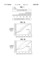
With a relatively high dielectric constant (20-25), an excellent step coverage, and a rather low leakage current after post-deposition annealing treatment, tantalum pentaoxide (Ta2 O5) films, made from chemical vapor deposited tantalum pentaoxide (CVD Ta2 O5), are one of the most common dielectric films. Schematic cross-sectional views of the structures of capacitors with single and composite films are shown in FIG. 1. A single Ta2 O5 layer film, noted as A, is formed on a phosphorus-doped polysilicon (n+ poly-Si) bottom electrode. On top of the Ta2 O5 dielectric film, a titanium nitride (TiN) and aluminum (Al) (not shown) top electrode is formed by reactive sputtering.
Recently, there is a growing interest in titanium dioxide (TiO2) because of its higher dielectric constant (30-100). In FIG. 1, the structure of the capacitor with a single TiO2 film noted as I is shown. Similar to the single Ta2 O5 dielectric film, the TiO2 dielectric film is formed on the bottom n+ poly-Si electrode, and with a TiN and Al electrode on top.
The capacitance per unit area of the above single dielectric films is graphically illustrated in FIG. 4. Due to the much higher dielectric constant in the TiO2 film (I), the capacitance of the capacitor with film I is much higher than the capacitance of the capacitor with film A. However, referring to FIG. 2a, FIG. 2b, FIG. 6a, and FIG. 6b, the leakage current of film I is the largest, and is the smallest in film A. The larger leakage current in film I is due to the lower energy band gap of the TiO2 film (3 eV to 4 eV for TiO2, and 4 eV to 5 eV for Ta2 O5) and to the film's microstructure, which will be discussed further hereinafter. In addition, the breakdown voltage distribution is shown in FIG. 3. Film A can sustain a higher voltage than film I.
It is therefore an object of the invention to provide a dielectric film with a higher dielectric constant, and thus, with a higher magnitude of capacitance.
It is a further object of the invention to provide a dielectric film with a satisfactory leakage current and a lower breakdown voltage.
To achieve these objects and advantages, and in accordance with the purpose of the invention, as embodied and broadly described herein, the invention is directed towards a composite dielectric film, comprising a phosphorus doped polysilicon bottom electrode. Rapid thermal nitridation is performed in ammonia at 900° C. for about 60 seconds for the phosphorus doped polysilicon bottom electrode. A first tantalum pentaoxide layer is formed on the phosphorus doped polysilicon bottom electrode by low pressure chemical vapor deposition from a mixture of pentaethoxyl tantalum and oxygen gas. A titanium dioxide layer is formed on the first tantalum pentaoxide layer by low pressure chemical vapor deposition from a mixture of tetra-isopropyl-titanate and oxygen gas. A second tantalum pentaoxide layer is formed on the titanium dioxide layer. After the deposition of the composite dielectric film, rapid thermal nitrous oxide annealing is performed at 800° C. for about 60 seconds. A titanium nitride and aluminum top electrode is formed by reactive sputtering.
It is to be understood that both the foregoing general description and the following detailed description are exemplary and explanatory only and are not restrictive of the invention, as claimed.
The accompanying drawings, which are incorporated in and constitute a part of the specification, illustrate an embodiment of the invention and together with the description, serve to explain the principles of the invention. In the drawings,
FIG. 1 is a cross-sectional view of various capacitors with single and composite dielectric films;
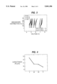
FIGS. 2(a) and FIG. 2(b) present the leakage current characteristics for single and double layer films under positive and negative polarities, respectively;
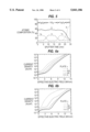
FIG. 3 shows the breakdown voltage distributions for single and double layer films;
FIG. 4 presents the capacitance per unit area of single and double layer films;
FIG. 5 is an AES depth of an AIA composite film;
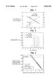
FIG. 6(a) and FIG. 6(b) present the leakage current characteristics for single and double layer films under positive and negative polarities, respectively;
FIG. 7 shows the critical voltage and capacitance per unit area as a function of single and triple layer films;
FIG. 8 presents a comparison of an A and AIA structure; and
FIG. 9 shows the lifetime extraction: time to 50% cumulative failure as a function of applied field for A and AIA structures.
Referring to FIG. 1, a double layer film, noted as AI, and composed of a Ta2 O5 (A) and TiO2 (I) film sequentially formed on an n+ poly-Si bottom electrode is shown. Also, another double layer film, noted as IA, and composed of film I and film A sequentially formed on the n+ poly-Si bottom electrode is shown in FIG. 1 as well. In this and the following embodiments, both films I and A are formed by low pressure chemical deposition from a mixture of O2 gas and a source gas, for example, tetra-isopropyl-titanate (Ti(OC3 H7)4, TPT) as a Ti source and pentaethoxy tantalum (Ta(OC5 H5)5) as a Ta precursor. For TiO2 deposition, the Ti source is vaporized at 60° C., and introduced into the reactor chamber using argon (Ar) gas. For Ta2 O5 deposition, the Ta source is vaporized at 100° C., and introduced into the reactor chamber. The deposition temperature of TiO2 and Ta2 O5 is 450° C. and 350° C., respectively. Prior to deposition, the sample is treated using rapid thermal nitridation (RTN) in NH3 at 900° C. for 60 seconds. After deposition, the sample is subjected to rapid thermal nitrous oxide (N2 O) annealing at 800° C. for 60 seconds. To be used as a MOS capacitor, Titanium nitride (TiN) and Al top electrodes are deposited on the film AI by reactive sputtering.
In FIG. 2a and FIG. 2b, the typical results of the leakage current characteristics of 10 nm single and double layers are shown. The effective electric field is calculated from the applied voltage and the equivalent SiO2 thickness extracted from C-V measurement at 100 kHz using a value of 3.82 for the SiO2 dielectric constant. For both polarities, a capacitor with film A shows the lowest leakage current, while a capacitor with film I exhibits the highest one. Noticeably, under positive polarity, the AI structure has a higher leakage current than the IA structure. This may be attributed to the reaction between the TiO2 and Ta2 O5 films during the post-deposition annealing treatment, in which the metallic Ta (Ti) existing in the Ta2 O5 (TiO2) film diffuses into the TiO2 (Ta2 O2) film. Owing to the stronger affinity for metallic Ti than for metallic Ta, the Ta in the TiO2 film acts as an interstitial, and leads to the increase of the leakage current. In this embodiment, the amounts of Ti diffusing in Ta2 O5 film can not be controlled and too much Ti results in a higher leakage current of the AI double layer as compared to the Ta2 O5 single layer. As shown in FIG. 2a and FIG. 2b, I and IA structures, in which the top layer is the TiO2 film, possess inferior leakage currents for negative bias than for positive bias. This may be attributed to a rougher surface of the TiO2 film than the Ta2 O5 film. In the case of I and IA structures, the surface roughness dominates over the effect of the work function difference between TiN and n+ poly-Si. These results demonstrate that the leakage current is always higher if electrons are injected from the TiO2 /electrode. This implies that the TiO2 and the contacting electrode play an important role in determining the electrical properties for composite films.
The breakdown voltage distribution is shown in FIG. 3. The Ta2 O5 layer has a higher breakdown voltage than the composite films. A capacitor with a TiO2 dielectric film has a higher capacitance than a capacitor with a Ta2 O5 film. The capacitance's for IA and AI are both higher than that for a Ta2 O5 single layer. This result suggests that the combination of TiO2 and Ta2 O5 films is useful to increase the capacitance as compared to a single layer Ta2 O5 film.
In spite of the higher capacitance behavior for the double layer structure, AI and IA are not optimal structures for composite films, based on the consideration of leakage current characteristics.
Referring again to FIG. 1, a triple layer film AIA and another triple layer film IAI are deposited on an n+ poly-Si bottom electrode. The method of deposition for both film A and film I are the same as for the first embodiment. Again, TiN and Al are used as the top electrode. FIG. 5 shows the AES depth profiles of the AIA structure. This result confirms the formation of multilayer structure.
FIG. 6a and FIG. 6b compares the leakage current characteristic of 15 nm I, AIA, IAI, and A structures. The capacitor with the IAI structure shows a superior leakage current than one with an I film, and has a higher leakage current compared to the AIA structure. The foregoing implies that the leakage current is inferior if electrons are injected from the TiO2 /electrode. Instead, with the injection of electrons from the Ta2 O5 /electrode, the capacitor with the AIA structure exhibits less leakage current. Moreover, the capacitors with A and AIA structures have similar leakage current characteristics for both polarities.
FIG. 7 shows the critical voltage required to induce a leakage current of 10 nA/cm2 and the capacitance per unit area as a function of structures. TiO2 has the highest capacitance but the lowest critical voltage. Ta2 O5 shows just the opposite results. Although the AIA structure has a slightly smaller Vcrit compared to the A structure, it possesses a 15% higher capacitance.
FIG. 8 shows the distribution of the critical electric field, defined at the electric field with a leakage current of 1 μA/cm2, of the A and AIA structures at positive and negative voltages, respectively. This result shows that the distribution of the AIA structure is similar to that of the A structure.
FIG. 9 shows the electric field dependence of time to 50% cumulative failure under both voltage stress polarities for the A and the AIA structures. This result reveals that the reliability of the composite film AIA is comparable to that of the Ta2 O5 single film.
Other embodiments of the invention will be apparent to those skilled in the art from consideration of the specification and practice of the invention disclosed herein. It is intended that the specification and examples be considered as exemplary only, with a true scope and spirit of the invention being indicated by the following claims.
Claims (8)
1. A composite dielectric film comprising:
an n+ polysilicon phosphorus-doped bottom electrode formed using rapid thermal nitration in ammonia at about 900° C. for about 60 seconds;
a titanium dioxide layer on the n+ Polysilicon bottom electrode;
a tantalum Pentaoxide layer on the titanium dioxide layer; and
a top electrode over the tantalum pentaoxide layer.
2. A composite dielectric film comprising:
an n+ Polysilicon bottom electrode;
a titanium dioxide layer formed on the n+ polysilicon bottom electrode using low pressure chemical vapor deposition:
from a mixture of tetra-isopropyl-titanate and oxygen gas;
vaporizing the tetra-isopropyl-titanate at about 60° C., and introducing the vaporized tetra-isopropyl-titanate into a reactor chamber using argon gas; and
at a deposition temperature of about 450° C.;
a tantalum pentaoxide layer on the titanium dioxide layer; and
a top electrode over the tantalum pentaoxide layer.
3. A composite dielectric film according to claim 1, comprising:
an n+ Polysilicon bottom electrode;
a titanium dioxide layer on the n+ polysilicon bottom electrode;
a tantalum pentaoxide layer formed on the titanium dioxide layer using low pressure chemical vapor deposition:
from a mixture of pentaethoxy tantalum and oxygen gas;
vaporizing the pentaethoxy tantalum at a temperature of about 100° C., and introducing the vaporized pentaethoxy tantalum into a reactor chamber using argon gas; and
at a deposition temperature of about 350° C., and
a top electrode over the tantalum pentaoxide layer.
4. The composite dielectric film according to claim 1, wherein the top electrode is a reactively sputtered and deposited titanium nitride and aluminum electrode.
5. A composite dielectric film, comprising:
a phosphorus doped polysilicon bottom electrode;
a first titanium dioxide layer on the phosphorus doped polysilicon bottom electrode;
a tantalum pentaoxide layer on the first titanium dioxide layer;
a second titanium dioxide layer on the tantalum pentaoxide layer; and
a titanium nitride and aluminum top electrode over the second titanium dioxide layer.
6. A composite dielectric film, comprising:
a phosphorus doped polysilicon bottom electrode;
a first tantalum pentaoxide layer on the phosphorus doped polysilicon bottom electrode;
a titanium dioxide layer on the first tantalum pentaoxide layer;
a second tantalum pentaoxide layer on the titanium dioxide layer; and
a titanium nitride and aluminum top electrode over the second tantalum pentaoxide layer.
7. The composite dielectric film according to claim 2, wherein the top electrode is a reactively sputtered and deposited titanium nitride and aluminum electrode.
8. The composite dielectric film according to claim 3, wherein the top electrode is a reactively sputtered and deposited titanium nitride and aluminum electrode.
Priority Applications (3)
| Application Number | Priority Date | Filing Date | Title |
|---|---|---|---|
| SG1997002961A SG63970A1 (en) | 1997-08-16 | 1997-08-16 | Composite dielectric films |
| US08/912,867 US5841186A (en) | 1997-08-19 | 1997-08-19 | Composite dielectric films |
| JP24082897A JPH1187623A (en) | 1997-08-19 | 1997-09-05 | Composite dielectric film |
Applications Claiming Priority (1)
| Application Number | Priority Date | Filing Date | Title |
|---|---|---|---|
| US08/912,867 US5841186A (en) | 1997-08-19 | 1997-08-19 | Composite dielectric films |
Publications (1)
| Publication Number | Publication Date |
|---|---|
| US5841186A true US5841186A (en) | 1998-11-24 |
Family
ID=25432584
Family Applications (1)
| Application Number | Title | Priority Date | Filing Date |
|---|---|---|---|
| US08/912,867 Expired - Fee Related US5841186A (en) | 1997-08-16 | 1997-08-19 | Composite dielectric films |
Country Status (1)
| Country | Link |
|---|---|
| US (1) | US5841186A (en) |
Cited By (13)
| Publication number | Priority date | Publication date | Assignee | Title |
|---|---|---|---|---|
| EP1022783A2 (en) * | 1999-01-12 | 2000-07-26 | Lucent Technologies Inc. | Integrated circuit device having dual damascene capacitor and associated method for making |
| US6218300B1 (en) * | 1998-06-12 | 2001-04-17 | Applied Materials, Inc. | Method and apparatus for forming a titanium doped tantalum pentaoxide dielectric layer using CVD |
| US6281066B1 (en) | 1998-12-22 | 2001-08-28 | Hyundai Electronics, Industries Co., Ltd. | Method of manufacturing a capacitor in a memory device |
| US20020074584A1 (en) * | 2000-12-20 | 2002-06-20 | Micron Technology, Inc. | Low leakage MIM capacitor |
| US6448128B1 (en) * | 1999-07-01 | 2002-09-10 | Hyundai Electronics Industries Co., Ltd. | Capacitor for semiconductor memory device and method of manufacturing the same |
| US20020167038A1 (en) * | 2000-08-30 | 2002-11-14 | Jiong-Ping Lu | Novel high-k dielectric materials and processes for manufacturing them |
| US6617206B1 (en) | 2000-06-07 | 2003-09-09 | Micron Technology, Inc. | Method of forming a capacitor structure |
| US20040082126A1 (en) * | 1999-12-22 | 2004-04-29 | Hyundai Electronics Industries Co., Ltd. | Semiconductor device incorporated therein high K capacitor dielectric and method for the manufacture thereof |
| US20040188045A1 (en) * | 2000-11-30 | 2004-09-30 | The Procter & Gamble Company | Low viscosity bilayer disrupted softening composition for tissue paper |
| US20040259383A1 (en) * | 2001-09-10 | 2004-12-23 | Choi Han-Mei | Method of forming a metal oxide film |
| US20050082593A1 (en) * | 2003-08-18 | 2005-04-21 | Samsung Electronics Co., Ltd. | Capacitor, method of manufacturing the same and memory device including the same |
| CN110415974A (en) * | 2019-07-17 | 2019-11-05 | 南京大学 | One kind is based on nano-stack structured metal oxide flexible capacitor and preparation method thereof |
| CN110676161A (en) * | 2019-09-27 | 2020-01-10 | 天津大学 | Double-layer material heterogeneous gate dielectric layer flexible silicon thin film transistor and manufacturing method thereof |
Citations (2)
| Publication number | Priority date | Publication date | Assignee | Title |
|---|---|---|---|---|
| US4987102A (en) * | 1989-12-04 | 1991-01-22 | Motorola, Inc. | Process for forming high purity thin films |
| US5406446A (en) * | 1993-04-29 | 1995-04-11 | Fujitsu Limited | Thin film capacitor |
-
1997
- 1997-08-19 US US08/912,867 patent/US5841186A/en not_active Expired - Fee Related
Patent Citations (2)
| Publication number | Priority date | Publication date | Assignee | Title |
|---|---|---|---|---|
| US4987102A (en) * | 1989-12-04 | 1991-01-22 | Motorola, Inc. | Process for forming high purity thin films |
| US5406446A (en) * | 1993-04-29 | 1995-04-11 | Fujitsu Limited | Thin film capacitor |
Cited By (38)
| Publication number | Priority date | Publication date | Assignee | Title |
|---|---|---|---|---|
| US6218300B1 (en) * | 1998-06-12 | 2001-04-17 | Applied Materials, Inc. | Method and apparatus for forming a titanium doped tantalum pentaoxide dielectric layer using CVD |
| US6281066B1 (en) | 1998-12-22 | 2001-08-28 | Hyundai Electronics, Industries Co., Ltd. | Method of manufacturing a capacitor in a memory device |
| EP1022783A2 (en) * | 1999-01-12 | 2000-07-26 | Lucent Technologies Inc. | Integrated circuit device having dual damascene capacitor and associated method for making |
| EP1022783A3 (en) * | 1999-01-12 | 2001-06-06 | Lucent Technologies Inc. | Integrated circuit device having dual damascene capacitor and associated method for making |
| US6320244B1 (en) | 1999-01-12 | 2001-11-20 | Agere Systems Guardian Corp. | Integrated circuit device having dual damascene capacitor |
| US6448128B1 (en) * | 1999-07-01 | 2002-09-10 | Hyundai Electronics Industries Co., Ltd. | Capacitor for semiconductor memory device and method of manufacturing the same |
| US6777740B2 (en) | 1999-07-01 | 2004-08-17 | Hyundai Electronics Industries Co., Ltd. | Capacitor for semiconductor memory device and method of manufacturing the same |
| US7012001B2 (en) * | 1999-12-22 | 2006-03-14 | Hyundai Electronics Industries Co., Ltd. | Method for manufacturing a semiconductor device for use in a memory cell that includes forming a composite layer of tantalum oxide and titanium oxide over a bottom capacitor electrode |
| US20040082126A1 (en) * | 1999-12-22 | 2004-04-29 | Hyundai Electronics Industries Co., Ltd. | Semiconductor device incorporated therein high K capacitor dielectric and method for the manufacture thereof |
| US8421140B2 (en) | 2000-06-07 | 2013-04-16 | Micron Technology, Inc. | Dielectric structures |
| US20060258113A1 (en) * | 2000-06-07 | 2006-11-16 | Micron Technology, Inc. | Capacitor structure |
| US6617206B1 (en) | 2000-06-07 | 2003-09-09 | Micron Technology, Inc. | Method of forming a capacitor structure |
| US20040097034A1 (en) * | 2000-06-07 | 2004-05-20 | Sandhu Gurtej S. | Capacitor structure |
| US20050167726A1 (en) * | 2000-08-30 | 2005-08-04 | Jiong-Ping Lu | Novel high-k dielectric materials and processes for manufacturing them |
| US20100227450A1 (en) * | 2000-08-30 | 2010-09-09 | Micron Technology, Inc. | Novel high-k dielectric materials and processes for manufacturing them |
| US8088659B2 (en) | 2000-08-30 | 2012-01-03 | Micron Technology, Inc. | Method of forming capacitors |
| US6861695B2 (en) * | 2000-08-30 | 2005-03-01 | Micron Technology, Inc. | High-k dielectric materials and processes for manufacturing them |
| US7732852B2 (en) | 2000-08-30 | 2010-06-08 | Micron Technology, Inc. | High-K dielectric materials and processes for manufacturing them |
| US6787429B2 (en) | 2000-08-30 | 2004-09-07 | Micron Technology, Inc. | High-K dielectric materials and processes for manufacturing them |
| US7544987B2 (en) | 2000-08-30 | 2009-06-09 | Micron Technology, Inc. | High-k dielectric materials and processes for manufacturing them |
| US20020167038A1 (en) * | 2000-08-30 | 2002-11-14 | Jiong-Ping Lu | Novel high-k dielectric materials and processes for manufacturing them |
| US20060270148A1 (en) * | 2000-08-30 | 2006-11-30 | Jiong-Ping Lu | Novel high-k dielectric materials and processes for manufacturing them |
| US20040188045A1 (en) * | 2000-11-30 | 2004-09-30 | The Procter & Gamble Company | Low viscosity bilayer disrupted softening composition for tissue paper |
| US20020192904A1 (en) * | 2000-12-20 | 2002-12-19 | Micron Technology, Inc. | Low leakage MIM capacitor |
| US20020074584A1 (en) * | 2000-12-20 | 2002-06-20 | Micron Technology, Inc. | Low leakage MIM capacitor |
| US20080064179A1 (en) * | 2000-12-20 | 2008-03-13 | Micron Technology, Inc. | Low leakage mim capacitor |
| US7368343B2 (en) | 2000-12-20 | 2008-05-06 | Micron Technology, Inc. | Low leakage MIM capacitor |
| US7378719B2 (en) | 2000-12-20 | 2008-05-27 | Micron Technology, Inc. | Low leakage MIM capacitor |
| US7435641B2 (en) | 2000-12-20 | 2008-10-14 | Micron Technology, Inc. | Low leakage MIM capacitor |
| US20080057663A1 (en) * | 2000-12-20 | 2008-03-06 | Micron Technology, Inc. | Low leakage mim capacitor |
| US8470665B2 (en) | 2000-12-20 | 2013-06-25 | Micron Technology, Inc. | Low leakage MIM capacitor |
| US20040259383A1 (en) * | 2001-09-10 | 2004-12-23 | Choi Han-Mei | Method of forming a metal oxide film |
| US7217669B2 (en) * | 2001-09-10 | 2007-05-15 | Samsung Electronics Co., Ltd. | Method of forming a metal oxide film |
| EP1508906A3 (en) * | 2003-08-18 | 2006-12-06 | Samsung Electronics Co., Ltd. | Capacitor, method of manufacturing the same and memory device including the same |
| US20090126173A1 (en) * | 2003-08-18 | 2009-05-21 | Samsung Electronics Co., Ltd. | Method of manufacturing a capacitor and memory device including the same |
| US20050082593A1 (en) * | 2003-08-18 | 2005-04-21 | Samsung Electronics Co., Ltd. | Capacitor, method of manufacturing the same and memory device including the same |
| CN110415974A (en) * | 2019-07-17 | 2019-11-05 | 南京大学 | One kind is based on nano-stack structured metal oxide flexible capacitor and preparation method thereof |
| CN110676161A (en) * | 2019-09-27 | 2020-01-10 | 天津大学 | Double-layer material heterogeneous gate dielectric layer flexible silicon thin film transistor and manufacturing method thereof |
Similar Documents
| Publication | Publication Date | Title |
|---|---|---|
| US5841186A (en) | Composite dielectric films | |
| JP3577189B2 (en) | Method for manufacturing capacitor of semiconductor device | |
| US5930584A (en) | Process for fabricating low leakage current electrode for LPCVD titanium oxide films | |
| US6201276B1 (en) | Method of fabricating semiconductor devices utilizing in situ passivation of dielectric thin films | |
| US6265260B1 (en) | Method for making an integrated circuit capacitor including tantalum pentoxide | |
| US6346746B1 (en) | Capacitor and electrode structures for a semiconductor device | |
| US6010940A (en) | Methods for fabricating CVD TiN barrier layers for capacitor structures | |
| US6573547B2 (en) | Method for forming cell capacitor for high-integrated DRAMs | |
| US6784100B2 (en) | Capacitor with oxidation barrier layer and method for manufacturing the same | |
| Sun et al. | Reduction of leakage current in chemical-vapor-deposited Ta/sub 2/O/sub 5/thin films by furnace N/sub 2/O annealing | |
| US20010029068A1 (en) | Semiconductor device structure including a tantalum pentoxide layer sandwiched between silicon nitride layers | |
| US6133086A (en) | Fabrication method of a tantalum pentoxide dielectric layer for a DRAM capacitor | |
| Kwon et al. | Ta/sub 2/O/sub 5/capacitors for 1 Gbit DRAM and beyond | |
| US6967135B1 (en) | Method of forming capacitor of semiconductor device | |
| JPH1187623A (en) | Composite dielectric film | |
| KR100410389B1 (en) | Method of forming a capacitor of a semiconductor device | |
| US6893963B2 (en) | Method for forming a titanium nitride layer | |
| KR19990024359A (en) | Composite dielectric membrane | |
| Han et al. | Effects of post-deposition annealing on the electrical properties and reliability of ultrathin chemical vapor deposited Ta/sub 2/O/sub 5/films | |
| KR100308885B1 (en) | Method for fabricating insulation layer of capacitor | |
| KR100335773B1 (en) | Method of manufacturing a capacitor in a semiconductor device | |
| US20020047148A1 (en) | Methods of manufacturing integrated circuit capacitors having ruthenium upper electrodes and capacitors formed thereby | |
| KR100414868B1 (en) | Method for fabricating capacitor | |
| KR100297100B1 (en) | Method of manufacturing a capacitor in a semiconductor device | |
| KR100249095B1 (en) | Process for fabricating low leakage current electrode for titanium oxide films |
Legal Events
| Date | Code | Title | Description |
|---|---|---|---|
| AS | Assignment |
Owner name: UNITED MICROELECTRONICS CORP., TAIWAN Free format text: ASSIGNMENT OF ASSIGNORS INTEREST;ASSIGNORS:SUN, SHI-CHUNG;CHEN, TSAI-FU;REEL/FRAME:008780/0397;SIGNING DATES FROM 19970731 TO 19970801 |
|
| FPAY | Fee payment |
Year of fee payment: 4 |
|
| FPAY | Fee payment |
Year of fee payment: 8 |
|
| REMI | Maintenance fee reminder mailed | ||
| LAPS | Lapse for failure to pay maintenance fees | ||
| STCH | Information on status: patent discontinuation |
Free format text: PATENT EXPIRED DUE TO NONPAYMENT OF MAINTENANCE FEES UNDER 37 CFR 1.362 |
|
| FP | Lapsed due to failure to pay maintenance fee |
Effective date: 20101124 |