US5817554A - Use of a grated top surface topography for capacitor structures - Google Patents
Use of a grated top surface topography for capacitor structures Download PDFInfo
- Publication number
- US5817554A US5817554A US08/813,723 US81372397A US5817554A US 5817554 A US5817554 A US 5817554A US 81372397 A US81372397 A US 81372397A US 5817554 A US5817554 A US 5817554A
- Authority
- US
- United States
- Prior art keywords
- layer
- polysilicon
- spots
- silicon oxide
- angstroms
- Prior art date
- Legal status (The legal status is an assumption and is not a legal conclusion. Google has not performed a legal analysis and makes no representation as to the accuracy of the status listed.)
- Expired - Lifetime
Links
Images


Classifications
-
- H—ELECTRICITY
- H01—ELECTRIC ELEMENTS
- H01L—SEMICONDUCTOR DEVICES NOT COVERED BY CLASS H10
- H01L28/00—Passive two-terminal components without a potential-jump or surface barrier for integrated circuits; Details thereof; Multistep manufacturing processes therefor
- H01L28/40—Capacitors
- H01L28/60—Electrodes
- H01L28/82—Electrodes with an enlarged surface, e.g. formed by texturisation
- H01L28/90—Electrodes with an enlarged surface, e.g. formed by texturisation having vertical extensions
- H01L28/92—Electrodes with an enlarged surface, e.g. formed by texturisation having vertical extensions made by patterning layers, e.g. by etching conductive layers
-
- H—ELECTRICITY
- H10—SEMICONDUCTOR DEVICES; ELECTRIC SOLID-STATE DEVICES NOT OTHERWISE PROVIDED FOR
- H10B—ELECTRONIC MEMORY DEVICES
- H10B12/00—Dynamic random access memory [DRAM] devices
- H10B12/01—Manufacture or treatment
- H10B12/02—Manufacture or treatment for one transistor one-capacitor [1T-1C] memory cells
- H10B12/03—Making the capacitor or connections thereto
- H10B12/033—Making the capacitor or connections thereto the capacitor extending over the transistor
Definitions
- the present invention relates to a method used to fabricate high density, semiconductor, DRAM cells, and more specifically to a process used to increase the surface area, and the accompanying capacitance of In STC component of the DRAM cell, via the use of a storage node electrode configuration, featuring a grated, top surface topography.
- DRAM dynamic random access memory
- STC stacked capacitor
- a DRAM cell is usually comprised of the STC structure, overlying a transfer gate transistor, and connected to the source of the transfer gate transistor.
- the decreasing size of the transfer gate transistor limits the dimensions of the STC structure.
- To increase the capacitance of the STC structure comprised of two electrodes, separated by a dielectric layer, either the thickness of the dielectric layer has to be decreased, or the area of the capacitor has to be increased. The reduction in dielectric thickness is limited by increasing reliability and yield risks, encountered with ultra thin dielectric layers.
- the area of the STC structure is limited by the area of the underlying transfer gate transistor dimensions.
- the advancement of the DRAM technology to densities of 16 million cells per chip, or greater, has resulted in a specific cell in which a smaller transfer gate transistor is being used, resulting in less of an overlying area for placement of overlying STC structures.
- HSG hemispherical grained
- the Watanabe, et al process although resulting in increased surface area, has the level of increased surface area limited by the height, or roughness of the HSG grains, which can be difficult to control and reproduce.
- Another process for increasing the surface area of a storage node electrode, via the use of an HSG process is shown by C. Y. Lu, in an invention disclosure, VIS85-111, (serial No. 08-734061, filed Oct. 18, 1996).
- This invention also describes the use of HSG, but in this case discontinuous spots of HSG are used as a mask to transfer the small diameter feature of the HSG spots, to an underlying silicon oxide layer.
- the small diameter features now in the form of silicon oxide spots, are then used as a mask to allow etching of an underlying polysilicon layer, exposed between silicon oxide spots, to occur, resulting in a top surface of polysilicon exhibiting increased surface area.
- This method allows the level of surface area increases to be controlled by the depth of etching into the underlying polysilicon layer, used for the storage node electrode.
- this invention although resulting in increased storage node surface areas, is complex, involving transferring the HSG spot feature to an underlying insulator, and then using the insulator spots as a mask for creating the storage node topography.
- This invention will describe another alternative for increasing the surface area of a polysilicon storage node electrode, by creating a grated, top surface topography, exhibiting a pattern of raised and lowered features in the polysilicon storage node.
- This grated, top surface topography is obtained via a process of initially depositing small diameter hemi-spherical grained, (HSG), spots, on a thin layer of silicon nitride, which in turn overlies a polysilicon layer, with the polysilicon layer to be used as the material for creation of the storage node electrode of a DRAM device.
- HSG small diameter hemi-spherical grained,
- the small diameter HSG polysilicon spots are oxidized to form silicon oxide spots, larger in diameter then the small diameter hemi-spherical polysilicon spots, and featuring smaller spaces between masking spots, then similar features described in the Lu invention.
- a dry etching procedure is then employed to transfer the image of the silicon oxide spots to the underlying thin silicon nitride layer, and into the polysilicon layer.
- the polysilicon layer now exhibits a grated, top surface topography, comprised of raised regions, regions protected by silicon oxide spots during the dry etch procedure, and lower regions, regions in which polysilicon was removed during the dry etching procedure.
- This invention using only the silicon oxide spots as a mask for creation of the grated, top surface topography, of a storage node electrode, simplifies the Lu invention, in which an intermediate layer, of small diameter insulator spots, obtained from overlying HSG polysiliocn spots, was needed for the formation of an underlying polysilicon layer, with increased topography.
- a transfer gate transistor comprised of: a thin gate insulator; a polysilicon gate structure, formed from a first polysilicon layer; lightly doped source and drain regions; insulator spacers on the sidewalls of the polysilicon gate structure; and heavily doped source and drain regions; are formed on a semiconductor substrate.
- a composite insulator layer comprised of a thin underlying silicon oxide layer, and a thick, overlying, doped oxide layer, is deposited, planarized, then followed by a contact hole opening in the composite insulator layer, made to expose the source and drain regions of adjacent transfer gate transistors.
- a second polysilicon layer is deposited, doped via use of in situ doping procedures, completely filling the contact hole opening, and contacting the source and drain regions of the transfer gate transistor.
- the second polysilicon layer also overlies the composite insulator layer, in regions outside the contact hole opening.
- a thin layer of silicon nitride is deposited on the underlying second polysilicon layer, followed by the deposition of a discontinuous layer of small diameter, HSG polysilicon spots.
- An oxidation procedure completely converts the small diameter HSG polysilicon spots to silicon oxide spots.
- An anisotropic reactive ion etch procedure is used, to etch the thin layer silicon nitride layer, exposed between silicon oxide spots, and to etch a top portion of second polysilicon layer, also exposed between the masking silicon oxide spots, creating a grated topography in the top surface of the second polysilicon layer, comprised of raised, unetched second polysilicon regions, and lower, etched second polysilicon regions. Removal of the silicon oxide spots, and the unetched silicon nitride, is followed by photolithographic and dry etching procedures, used to create the bottom electrode, or polysilicon storage node electrode shape, in the second polysilicon layer.
- a capacitor dielectric layer is next formed on the polysilicon storage node electrode structure, followed by the creation of an upper polysilicon electrode, or plate electrode structure, completing the processing of the STC structure.
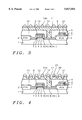
- FIGS. 1-7 which schematically shows, in cross-sectional style, the key fabrication stages used in the creation of a DRAM device, with a STC structure, with an increased surface area, resulting from a polysilicon storage node electrode structure, featuring a grated, top surface topography.
- the method of forming a DRAM device, with increased capacitance, resulting from the use of a STC structure that features a polysilicon storage node electrode, with increased surface area resulting from a grated, top surface topography, will now be described.
- the transfer gate transistor, used for this DRAM device, in this invention will be an N channel device.
- the STC structure, with the increased surface area described in this invention can also be applied to P channel, transfer gate transistor.
- FOX regions, 2 are used for purposes of isolation. Briefly the FOX regions, 2, are formed via thermal oxidation, in an oxygen-steam ambient, at a temperature between about 850° to 1050° C., to a thickness between about 3000 to 5000 Angstroms. A patterned oxidation resistant mask of silicon nitride-silicon oxide is used to prevent FOX regions, 2, from growing on areas of substrate, 1, to be used for subsequent device regions.
- the oxidation resistant mask is removed via use of a hot phosphoric acid solution for the overlying, silicon nitride layer, and a buffered hydrofluoric acid solution for the underlying silicon oxide layer.
- a gate insulator layer, 3, of silicon oxide is thermally grown in an oxygen-steam ambient, at a temperature between about 850° to 1050° C., to a thickness between about 50 to 200 Angstroms.
- a first polysilicon layer, 4, is next deposited using low pressure chemical vapor deposition, (LPCVD), procedures, at a temperature between about 500° to 700° C., to a thickness between about 1500 to 4000 Angstroms.
- LPCVD low pressure chemical vapor deposition
- the polysilicon can either be grown intrinsically and doped via ion implantation of arsenic or phosphorous, at an energy between about 30 to 80 KeV, at a dose between about 1E13 to 1E16 atoms/cm 2 , or grown using in situ doping procedures, via the incorporation of either arsine or phosphine to the silane ambient.
- a first silicon oxide layer, 5, used as a cap insulator layer, is next grown via the use of either LPCVD or plasma enhanced chemical vapor deposition, (PECVD), procedures, to a thickness between about 600 to 1500 Angstroms.
- Photolithographic and reactive ion etching, (RIE), procedures, using CHF 3 as an etchant for silicon oxide layer, 5, and using C1 2 as an etchant for polysilicon layer, 4, are used to create polysilicon gate structures, 4, with overlying cap insulator layer, 5, shown schematically in FIG. 1.
- Photoresist removal is accomplished via plasma oxygen ashing and careful wet cleans.
- a lightly doped source and drain region, 6, is next formed via ion implantation of phosphorous, at an energy between about 20 to 50 KeV, at a dose between about 1E13 to 1E14 atoms/cm 2 .
- a second insulator layer of silicon oxide is then deposited using either LPCVD or PECVD procedures, at a temperature between about 400° to 700° C., to a thickness between about 1500 to 4000 Angstroms, followed by an anisotropic RIE procedure, using CHF 3 as an etchant, creating insulator spacer, 7, on the sidewalls of polysilicon gate structures, 4.
- a heavily doped source and drain region, 8 is then formed via ion implantation of arsenic, at an energy between about 30 to 100 KeV, at a dose between about 1E14 to 5E16 atoms/cm 2 .
- the result of these procedures are schematically shown in FIG. 1.
- a third insulator layer of undoped silicon oxide, 9, is next deposited using LPCVD or PECVD procedures, at a temperature between about 700° to 750° C., to a thickness between about 1000 to 1500 Angstroms.
- a layer of doped silicon oxide, 10, either boro-phosphosilicate glass, (BPSG), or phosphosilicate glass, (PSG) is next deposited, using PECVD procedures, at a temperature between about 600° to 800° C., to a thickness between about 3000 to 6000 Angstroms, using tetraethylorthosilicate, (TEOS) as a source with the addition of either diborane and phosphine, for the BPSG layer, or the addition of only phosphine, for the PSG layer.
- TEOS tetraethylorthosilicate
- Insulator layer 9, and insulator 10 can be replaced by a single doped, or undoped insulator layer, if desired).
- Doped oxide layer, 10, is planarized using chemical mechanical polishing, to provide a smoother surface for subsequent depositions and patterning procedures. The result of these depositions and planarization procedures are again schematically shown in FIG. 1.
- Conventional photolithographic and RIE procedures, using CHF 3 as an etchant, are used to open contact hole, 11, in doped silicon oxide layer 10, and in silicon oxide layer, 9, exposing the top surface of heavily doped source and drain region, 8, again shown schematically in FIG. 1. Photoresist removal is performed via use of plasma oxygen ashing and careful wet cleans.
- a second layer of polysilicon layer, 12, is next deposited, via LPCVD procedures, at a temperature between about 500° to 700° C., to a thickness between about 2000 to 6000 Angstroms.
- Polysilicon layer, 12, can be deposited intrinsically and doped via ion implantation of either phosphorous or arsenic, or polysilicon layer, 12, can be deposited using in situ doping procedures, via the addition of either phosphine or arsine, to a silane ambient.
- polysilicon layer, 12 has an N type doping concentration of between 1E20 to 1E21 atoms/cm 3 .
- a thin layer of silicon nitride, 13, is deposited using either LPCVD or PECVD procedures, at a temperature between about 600° to 700° C., to a thickness between about 300 to 800 Angstroms.
- a critical deposition of intrinsic, hemi-spherical grained, (HSG), polysilicon, 14a, is next deposited, on silicon nitride layer, 13, at a temperature between about 500° to 700° C., to a thickness in which the intrinsic HSG polysilicon is discontinuous, resulting in small diameter HSG polysilicon spots, 14a, between about 100 to 1000 Angstroms in thickness, with a diameter between about 50 to 500 Angstroms, and with a space between small diameter HSG polysilicon spots, 14a, between about 100 to 1000 Angstroms.
- This is shown schematically in FIG. 2.
- Another alternative is to use dots of single crystalline silicon, comprised of with similar thickness and diameter as the HSG polysilicon spots, 14a, in place of the HSG polysilicon spots, 14a.
- Silicon oxide spots, 14b are between about 200 to 1000 Angstroms in thickness, with a diameter, larger then the diameter of the small diameter HSG polysilicon spots, 14a.
- Thin silicon nitride layer, 13, exposed between small diameter HSG polysilicon spots, 14a protects underlying second polysilicon layer, 12, from the oxidation procedure.
- a critical reactive ion etching, (RIE), procedure is next performed using Cl 2 as an etchant, using silicon oxide spots, 14b, as a mask.
- the RIE procedures completely removes thin silicon nitride layer, 13, exposed between silicon oxide spots, 14b, and continues removing exposed second polysilicon layer, 12, shown schematically in FIG. 4.
- the rounded corners of the lower, etched features, 30, result from the conditions used in the chemical dry etch procedure used to transfer the image of silicon oxide spots, 14b, to the polysilicon layer, 12.
- the masking silicon oxide spots, 14b are next removed via a buffered hydrofluoric acid solution, while regions of remaining, thin silicon nitride layer, 13, are removed using a hot phosphoric acid solution.
- the resulting second polysilicon layer, 12, with a grated, top surface topography is schematically show in FIG. 5.
- FIG. 6, schematically shows the patterning of second polysilicon layer, 12, featuring a grated, top surface topography.
- Photoresist shape, 15, is used as a mask, during a RIE procedure, using C1 2 as an etchant, used to define polysilicon storage node electrode, 16.
- Polysilicon storage node electrode, 16, offers increased surface area, obtained via use of the grated, top surface topography, of second polysilicon layer, 12. Removal of photoresist shape, 15, is accomplished via plasma oxygen ashing, and careful wet cleans.
- FIG. 7, schematically shows the completion of the STC structure.
- a dielectric layer, 17, is formed, overlying the polysilicon storage node electrode, 16.
- Dielectric layer, 17, can be an insulator layer possessing a high dielectric constant, such as Ta 2 O 5 , obtained via r.f sputtering techniques, at a thickness between about 10 to 100 Angstroms.
- Dielectric layer, 17, can also be ONO, (Oxidized--silicon Nitride--silicon Oxide).
- the ONO layer is formed by initially growing a silicon dioxide layer, between about 10 to 50 Angstroms, followed by the deposition of a silicon nitride layer, between about 10 to 20 Angstroms.
Abstract
Description
Claims (23)
Priority Applications (1)
| Application Number | Priority Date | Filing Date | Title |
|---|---|---|---|
| US08/813,723 US5817554A (en) | 1997-03-07 | 1997-03-07 | Use of a grated top surface topography for capacitor structures |
Applications Claiming Priority (1)
| Application Number | Priority Date | Filing Date | Title |
|---|---|---|---|
| US08/813,723 US5817554A (en) | 1997-03-07 | 1997-03-07 | Use of a grated top surface topography for capacitor structures |
Publications (1)
| Publication Number | Publication Date |
|---|---|
| US5817554A true US5817554A (en) | 1998-10-06 |
Family
ID=25213194
Family Applications (1)
| Application Number | Title | Priority Date | Filing Date |
|---|---|---|---|
| US08/813,723 Expired - Lifetime US5817554A (en) | 1997-03-07 | 1997-03-07 | Use of a grated top surface topography for capacitor structures |
Country Status (1)
| Country | Link |
|---|---|
| US (1) | US5817554A (en) |
Cited By (10)
| Publication number | Priority date | Publication date | Assignee | Title |
|---|---|---|---|---|
| US5888866A (en) * | 1998-04-18 | 1999-03-30 | United Microelectronics Corp. | Method for fabricating capacitors of a dynamic random access memory |
| US5897352A (en) * | 1998-03-25 | 1999-04-27 | Vanguard International Semiconductor Corporation | Method of manufacturing hemispherical grained polysilicon with improved adhesion and reduced capacitance depletion |
| US5907782A (en) * | 1998-08-15 | 1999-05-25 | Acer Semiconductor Manufacturing Inc. | Method of forming a multiple fin-pillar capacitor for a high density dram cell |
| US5923973A (en) * | 1997-10-24 | 1999-07-13 | Vanguard International Semiconductor Corporation | Method of making greek letter psi shaped capacitor for DRAM circuits |
| US5960295A (en) * | 1997-09-24 | 1999-09-28 | Nan Ya Technology Corporation | Method for fabricating a storage plate of a semiconductor capacitor |
| US6127221A (en) * | 1998-09-10 | 2000-10-03 | Vanguard International Semiconductor Corporation | In situ, one step, formation of selective hemispherical grain silicon layer, and a nitride-oxide dielectric capacitor layer, for a DRAM application |
| US6188097B1 (en) | 1997-07-02 | 2001-02-13 | Micron Technology, Inc. | Rough electrode (high surface area) from Ti and TiN |
| US6236080B1 (en) * | 1999-07-22 | 2001-05-22 | Worldwide Semiconductor Manufacturing Corp. | Method of manufacturing a capacitor for high density DRAMs |
| US6265263B1 (en) * | 1998-02-19 | 2001-07-24 | Texas Instruments - Acer Incorporated | Method for forming a DRAM capacitor with porous storage node and rugged sidewalls |
| US6297116B1 (en) * | 1999-02-05 | 2001-10-02 | Winbond Electronics Corp. | Method for manufacturing a metal oxide semiconductor (MOS)-based structure |
Citations (5)
| Publication number | Priority date | Publication date | Assignee | Title |
|---|---|---|---|---|
| US5254503A (en) * | 1992-06-02 | 1993-10-19 | International Business Machines Corporation | Process of making and using micro mask |
| US5302540A (en) * | 1991-11-16 | 1994-04-12 | Samsung Electronics Co., Ltd. | Method of making capacitor |
| US5342800A (en) * | 1991-11-12 | 1994-08-30 | Goldstar Electron Co., Ltd. | Method of making memory cell capacitor |
| US5358888A (en) * | 1991-12-18 | 1994-10-25 | Samsung Electronics Co., Ltd. | Method for manufacturing a capacitor of an integrated semiconductor device having increased surface area |
| US5492848A (en) * | 1994-03-18 | 1996-02-20 | United Microelectronics Corp. | Stacked capacitor process using silicon nodules |
-
1997
- 1997-03-07 US US08/813,723 patent/US5817554A/en not_active Expired - Lifetime
Patent Citations (5)
| Publication number | Priority date | Publication date | Assignee | Title |
|---|---|---|---|---|
| US5342800A (en) * | 1991-11-12 | 1994-08-30 | Goldstar Electron Co., Ltd. | Method of making memory cell capacitor |
| US5302540A (en) * | 1991-11-16 | 1994-04-12 | Samsung Electronics Co., Ltd. | Method of making capacitor |
| US5358888A (en) * | 1991-12-18 | 1994-10-25 | Samsung Electronics Co., Ltd. | Method for manufacturing a capacitor of an integrated semiconductor device having increased surface area |
| US5254503A (en) * | 1992-06-02 | 1993-10-19 | International Business Machines Corporation | Process of making and using micro mask |
| US5492848A (en) * | 1994-03-18 | 1996-02-20 | United Microelectronics Corp. | Stacked capacitor process using silicon nodules |
Non-Patent Citations (2)
| Title |
|---|
| Watanabe et al, "Hemispherical Gran Silicon for High Density DRAMs", Solid State Technology, Jul. 1992, pp. 29-33. |
| Watanabe et al, Hemispherical Gran Silicon for High Density DRAMs , Solid State Technology, Jul. 1992, pp. 29 33. * |
Cited By (15)
| Publication number | Priority date | Publication date | Assignee | Title |
|---|---|---|---|---|
| US6238994B1 (en) * | 1997-07-02 | 2001-05-29 | Micron Technology, Inc. | Method of creating a rough electrode (high surface area) from Ti and TiN and resulting article |
| US6902985B2 (en) | 1997-07-02 | 2005-06-07 | Micron Technology, Inc. | Method of forming a rough (high surface area) electrode from Ti and TiN capacitors and semiconductor devices including same |
| US6608343B2 (en) | 1997-07-02 | 2003-08-19 | Micron Technology, Inc. | Rough (high surface area) electrode from Ti and TiN, capacitors and semiconductor devices including same |
| US20020187607A1 (en) * | 1997-07-02 | 2002-12-12 | Derderian Garo J. | Method of forming a rough (high surface area) electrode from Ti and TiN capacitors and semiconductor devices including same |
| US6399982B1 (en) | 1997-07-02 | 2002-06-04 | Micron Technology, Inc. | Rough (high surface area) electrode from Ti and TiN capacitors and semiconductor devices including same |
| US6188097B1 (en) | 1997-07-02 | 2001-02-13 | Micron Technology, Inc. | Rough electrode (high surface area) from Ti and TiN |
| US5960295A (en) * | 1997-09-24 | 1999-09-28 | Nan Ya Technology Corporation | Method for fabricating a storage plate of a semiconductor capacitor |
| US5923973A (en) * | 1997-10-24 | 1999-07-13 | Vanguard International Semiconductor Corporation | Method of making greek letter psi shaped capacitor for DRAM circuits |
| US6265263B1 (en) * | 1998-02-19 | 2001-07-24 | Texas Instruments - Acer Incorporated | Method for forming a DRAM capacitor with porous storage node and rugged sidewalls |
| US5897352A (en) * | 1998-03-25 | 1999-04-27 | Vanguard International Semiconductor Corporation | Method of manufacturing hemispherical grained polysilicon with improved adhesion and reduced capacitance depletion |
| US5888866A (en) * | 1998-04-18 | 1999-03-30 | United Microelectronics Corp. | Method for fabricating capacitors of a dynamic random access memory |
| US5907782A (en) * | 1998-08-15 | 1999-05-25 | Acer Semiconductor Manufacturing Inc. | Method of forming a multiple fin-pillar capacitor for a high density dram cell |
| US6127221A (en) * | 1998-09-10 | 2000-10-03 | Vanguard International Semiconductor Corporation | In situ, one step, formation of selective hemispherical grain silicon layer, and a nitride-oxide dielectric capacitor layer, for a DRAM application |
| US6297116B1 (en) * | 1999-02-05 | 2001-10-02 | Winbond Electronics Corp. | Method for manufacturing a metal oxide semiconductor (MOS)-based structure |
| US6236080B1 (en) * | 1999-07-22 | 2001-05-22 | Worldwide Semiconductor Manufacturing Corp. | Method of manufacturing a capacitor for high density DRAMs |
Similar Documents
| Publication | Publication Date | Title |
|---|---|---|
| US5716883A (en) | Method of making increased surface area, storage node electrode, with narrow spaces between polysilicon columns | |
| US5150276A (en) | Method of fabricating a vertical parallel cell capacitor having a storage node capacitor plate comprising a center fin effecting electrical communication between itself and parallel annular rings | |
| US5913119A (en) | Method of selective growth of a hemispherical grain silicon layer on the outer sides of a crown shaped DRAM capacitor structure | |
| US5650351A (en) | Method to form a capacitor having multiple pillars for advanced DRAMS | |
| US5763306A (en) | Method of fabricating capacitor over bit line COB structure for a very high density DRAM applications | |
| US6479341B1 (en) | Capacitor over metal DRAM structure | |
| US5498562A (en) | Semiconductor processing methods of forming stacked capacitors | |
| US5240871A (en) | Corrugated storage contact capacitor and method for forming a corrugated storage contact capacitor | |
| US5350707A (en) | Method for making a capacitor having an electrode surface with a plurality of trenches formed therein | |
| US5362665A (en) | Method of making vertical DRAM cross point memory cell | |
| US5594682A (en) | High density self-aligned stack in trench DRAM technology | |
| US5604146A (en) | Method to fabricate a semiconductor memory device having an E-shaped storage node | |
| US5877052A (en) | Resolution of hemispherical grained silicon peeling and row-disturb problems for dynamic random access memory, stacked capacitor structures | |
| US6037220A (en) | Method of increasing the surface area of a DRAM capacitor structure via the use of hemispherical grained polysilicon | |
| US5793077A (en) | DRAM trench capacitor with recessed pillar | |
| US5858838A (en) | Method for increasing DRAM capacitance via use of a roughened surface bottom capacitor plate | |
| US6165839A (en) | Process to fabricate a cylindrical, capacitor structure under a bit line structure for a dynamic random access memory cell | |
| US6200898B1 (en) | Global planarization process for high step DRAM devices via use of HF vapor etching | |
| US6100137A (en) | Etch stop layer used for the fabrication of an overlying crown shaped storage node structure | |
| US5897352A (en) | Method of manufacturing hemispherical grained polysilicon with improved adhesion and reduced capacitance depletion | |
| US6037219A (en) | One step in situ doped amorphous silicon layers used for selective hemispherical grain silicon formation for crown shaped capacitor applications | |
| US5753551A (en) | Memory cell array with a self-aligned, buried bit line | |
| US6300191B1 (en) | Method of fabricating a capacitor under bit line structure for a dynamic random access memory device | |
| US6027969A (en) | Capacitor structure for a dynamic random access memory cell | |
| US5817554A (en) | Use of a grated top surface topography for capacitor structures |
Legal Events
| Date | Code | Title | Description |
|---|---|---|---|
| AS | Assignment |
Owner name: VANGUARD INTERNATIONAL SEMICONDUCTOR CORPORATION, Free format text: ASSIGNMENT OF ASSIGNORS INTEREST;ASSIGNOR:TSENG, HORNG-HUEI;REEL/FRAME:008463/0593 Effective date: 19970226 |
|
| STCF | Information on status: patent grant |
Free format text: PATENTED CASE |
|
| FPAY | Fee payment |
Year of fee payment: 4 |
|
| FPAY | Fee payment |
Year of fee payment: 8 |
|
| FPAY | Fee payment |
Year of fee payment: 12 |
|
| FEPP | Fee payment procedure |
Free format text: PAYER NUMBER DE-ASSIGNED (ORIGINAL EVENT CODE: RMPN); ENTITY STATUS OF PATENT OWNER: LARGE ENTITY Free format text: PAYOR NUMBER ASSIGNED (ORIGINAL EVENT CODE: ASPN); ENTITY STATUS OF PATENT OWNER: LARGE ENTITY |
|
| AS | Assignment |
Owner name: TAIWAN SEMICONDUCTOR MANUFACTURING CO., LTD., TAIW Free format text: ASSIGNMENT OF ASSIGNORS INTEREST;ASSIGNOR:VANGUARD INTERNATIONAL SEMICONDUCTOR CORPORATION;REEL/FRAME:025645/0397 Effective date: 20101026 |