US5796979A - Data processing system having demand based write through cache with enforced ordering - Google Patents
Data processing system having demand based write through cache with enforced ordering Download PDFInfo
- Publication number
- US5796979A US5796979A US08/730,994 US73099496A US5796979A US 5796979 A US5796979 A US 5796979A US 73099496 A US73099496 A US 73099496A US 5796979 A US5796979 A US 5796979A
- Authority
- US
- United States
- Prior art keywords
- cache
- write
- data
- memory
- system memory
- Prior art date
- Legal status (The legal status is an assumption and is not a legal conclusion. Google has not performed a legal analysis and makes no representation as to the accuracy of the status listed.)
- Expired - Fee Related
Links
Images


Classifications
-
- G—PHYSICS
- G06—COMPUTING; CALCULATING OR COUNTING
- G06F—ELECTRIC DIGITAL DATA PROCESSING
- G06F13/00—Interconnection of, or transfer of information or other signals between, memories, input/output devices or central processing units
- G06F13/14—Handling requests for interconnection or transfer
-
- G—PHYSICS
- G06—COMPUTING; CALCULATING OR COUNTING
- G06F—ELECTRIC DIGITAL DATA PROCESSING
- G06F12/00—Accessing, addressing or allocating within memory systems or architectures
- G06F12/02—Addressing or allocation; Relocation
- G06F12/08—Addressing or allocation; Relocation in hierarchically structured memory systems, e.g. virtual memory systems
- G06F12/0802—Addressing of a memory level in which the access to the desired data or data block requires associative addressing means, e.g. caches
- G06F12/0866—Addressing of a memory level in which the access to the desired data or data block requires associative addressing means, e.g. caches for peripheral storage systems, e.g. disk cache
-
- G—PHYSICS
- G06—COMPUTING; CALCULATING OR COUNTING
- G06F—ELECTRIC DIGITAL DATA PROCESSING
- G06F12/00—Accessing, addressing or allocating within memory systems or architectures
- G06F12/02—Addressing or allocation; Relocation
- G06F12/08—Addressing or allocation; Relocation in hierarchically structured memory systems, e.g. virtual memory systems
- G06F12/0802—Addressing of a memory level in which the access to the desired data or data block requires associative addressing means, e.g. caches
- G06F12/0806—Multiuser, multiprocessor or multiprocessing cache systems
- G06F12/0815—Cache consistency protocols
- G06F12/0831—Cache consistency protocols using a bus scheme, e.g. with bus monitoring or watching means
- G06F12/0835—Cache consistency protocols using a bus scheme, e.g. with bus monitoring or watching means for main memory peripheral accesses (e.g. I/O or DMA)
-
- G—PHYSICS
- G06—COMPUTING; CALCULATING OR COUNTING
- G06F—ELECTRIC DIGITAL DATA PROCESSING
- G06F2212/00—Indexing scheme relating to accessing, addressing or allocation within memory systems or architectures
- G06F2212/30—Providing cache or TLB in specific location of a processing system
- G06F2212/303—In peripheral interface, e.g. I/O adapter or channel
Definitions
- the present invention relates to data processing systems, and more particularly to data processing systems having one or more processors, a system storage, a system bus and one or more input/output channel controllers ("IOCC") and allowing direct memory access (DMA) from I/O channel controllers to system memory.
- IOCC input/output channel controllers
- DMA direct memory access
- Direct memory access is almost as old as the computer industry. It was first developed by Carl Christiansen, et al. for the IBM 705 computer system in 1956. The Christiansen, et al. U.S. Pat. No. 3,812,475 showed the basic DMA techniques employed in a Von Neumann computer architecture system.
- DMA techniques for systems including caches and write through caches are generally well-known in the art.
- a typical write through cache forwards each cache modification with an appropriate system memory modification.
- an equivalent multiple of system memory write operations occur.
- Write through caches are typically used in computer systems to reduce cache controller complexity and minimize cache and memory data inconsistencies.
- Processors, IOCCs and I/O devices commonly use traditional write through caches in order to obtain these benefits.
- a data processing system includes a processor, a system memory, one or more input/output channel controllers (IOCC), and a system bus connecting the processor, the memory and the IOCCs together for communicating instructions, address and data between the various elements of a system.
- the IOCC includes a paged cache storage having a number of lines wherein each line of the page may be, for example, 32 bytes.
- Each page in the cache also has several attribute bits for that page including the so called WIM and attribute bits.
- the W bit is for controlling write through operations; the I bit controls cache inhibit; and the M bit controls memory coherency. Since the IOCC is unaware of these page table attribute bits for the cache lines being DMAed to system memory, IOCC must maintain memory consistency and cache coherency without sacrificing performance.
- the method and apparatus according to the present invention provides high performance write through caches by gathering write data and performing block writes to system memory based on predetermined demand criteria.
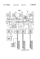
- FIG. 1 is a system block diagram of a data processing system embodying the present invention.
- FIG. 2 is a block diagram of a demand based write through cache in accordance with the present invention.
- FIG. 3 is a flow chart describing the operation of the demand based write through cache technique in accordance with the present invention.
- Multiprocessor system 100 includes a number of processing units 102, 104, 106 operatively connected to a system bus 108. Also connected to the system bus 108 is a memory controller 110, which controls access to system memory 112, and I/O channel controllers 114, 116, and 118. Additionally, a high performance I/O device 120 may be connected to the system bus 108.
- system controller 130 which communicates with each unit connected to the system bus 108 by point to point lines such as 132 to processor 102, 134 to processor 104, 136 to processor 106, 140 to memory controller 110, 144 to I/O channel controller 114, 146 to I/O channel controller 116, 148 to I/O channel controller 118, and 150 to high performance I/O device 120. Requests and grants of bus access are all controlled by system controller 130.
- I/O channel controller 114 controls and is connected to system I/O subsystem and native I/O subsystem 160.
- Each processor unit 102, 104, 106 may include a processor and a cache storage device.
- Cache 200 is organized as a 128 byte circular cache having two 64-byte cache lines wherein the cache is divided into four 32-byte sectors 202, 204, 206 and 208. From the system bus, this cache structure allows the IOCC, for example, IOCC 114 (see FIG. 1) to efficiently support systems with either 32-byte or 64-byte coherency requirements. Due to the coherency requirements of the system bus, there are many cases in which DMA write data by the IOCC is retried on the system bus for lengthy periods of time.
- the DMA write cache organization provides a relatively efficient means of isolating system bus traffic from I/O bus transfers, thus improving I/O bus throughput and bandwidth.
- IOCC 114 By organizing cache 200 as four 32-byte sectors, coupled with the circular structure of cache 200, IOCC 114 performs heavy pipelining of sequential write data thus allowing the I/O bus devices to sustain a high data rate via the I/O bus interface controller 250.
- the WIM attribute bits associated with system memory pages are shown in the following table with the meaning of each combination of WIM bits.
- WIM bits are managed by the operating system software and are accessed by processor 102, etc. (and I/O devices) to determine the cache attributes associated with each system memory page. Unlike processor 102, most IOCCs 114, etc. and I/O devices are unaware of the value of the WIM attribute bits. Thus, during I/O DMA write operations to system memory 112, IOCC 114 must support the 101 code in order to avoid I/O cache and memory data inconsistencies. This then allows IOCC 114 to extend the 101 code and support a demand based write through cache. In some systems, IOCC 114 is aware of the WIM attribute bits and supports demand based write through cache if the WIM bits equal the 101 code.
- the operation of the demand based write through cache will be described. If a demand based write through cache operation is to be performed, the WIM bits will be "101".
- the process tests for an I/O DMA write operation step 310.
- the process loops until the write operation is received.
- the process then proceeds to write the data in the IOCC cache at step 320.
- the process loops until all data is written into the IOCC cache (step 320) at which time the process then moves to step 330, which is the hold write operation to system step.
- the hold write operation to system memory at 330 is employed to cause the process to wait until one of several events occurs and then allow a block write of the held modified data to system memory.
- Test is made at step 340 to determine whether the I/O device has:
- step 340 If none of these events have occurred, the process loops back to step 320 to allow additional data to be written into the cache of the IOCC (i.e., 114). If any of the events set forth in step 340 have occurred, a block write of modified data to system memory 112 is then performed at step 350.
- Another feature of the present invention relates to maintaining write ordering to system memory.
- coherency mechanisms such as cache level snooping, retry and push protocols have been used to maintain write ordering between cache and system memory. (Snooping, retry, and push protocols are well known in the art).
- the apparatus and method according to the present invention having a demand based write through cache can significantly improve system performance and reduce design complexity by providing a byte level write ordering rather than cache level snooping, retry or push.
- Byte level ordering is achieved in a demand based write through cache by adding another condition to the demand criteria. This condition checks to determine if the I/O bus master ever writes "backwards" within the same cache line. That is, if address B is less than address A in the same line, then the write operation for B is held off until the demand based write through cache data is forwarded to system memory.
- I/O cache coherency and write data ordering are achieved without the IOCC ever having to snoop, retry or push the DMA write data.
Abstract
A data processing system includes a processor, a system memory, one or more input/output channel controllers (IOCC), and a system bus connecting the processor, the memory and the IOCCs together for communicating instructions, address and data between the various elements of a system. The IOCC includes a paged cache storage having a number of lines wherein each line of the page may be, for example, 32 bytes. Each page in the cache also has several attribute bits for that page including the so called WIM and attribute bits. The W bit is for controlling write through operations; the I bit controls cache inhibit; and the M bit controls memory coherency. Since the IOCC is unaware of these page table attribute bits for the cache lines being DMAed to system memory, IOCC must maintain memory consistency and cache coherency without sacrificing performance. For DMA write data to system memory, new cache attributes called global, cachable and demand based write through are created. Individual writes within a cache line are gathered by the IOCC and only written to system memory when the I/O bus master accesses a different cache line or relinquishes the I/O bus.
Description
This application is a continuation of application Ser. No. 08,316,979, filed on Oct. 3, 1994, which was abandoned upon the filing hereof.
This application for patent is related to the following applications for patent filed concurrently herewith:
EFFICIENT ADDRESS TRANSFER TECHNIQUE FOR A DATA PROCESSING SYSTEM, Ser. No. 08/317,007;
DUAL LATENCY STATUS AND COHERENCY REPORTING FOR A MULTIPROCESSING SYSTEM, Ser. No. 08/316,980 now U.S. Pat. No. 5,608,878;
SYSTEM AND METHOD FOR DETERMINING SOURCE OF DATA IN A SYSTEM WITH INTERVENING CACHES, Ser. No. 08/317,256;
QUEUED ARBITRATION MECHANISM FOR DATA PROCESSING SYSTEM, Ser. No. 08/317,006;
METHOD AND APPARATUS FOR REMOTE RETRY IN A DATA PROCESSING SYSTEM, Ser. No. 08/316,978 now U.S. Pat. No. 5,623,694;
ARRAY CLOCKING METHOD AND APPARATUS FOR INPUT/OUTPUT SUBSYSTEMS, Ser. No. 08/316,976 now U.S. Pat. No. 5,548,797;
COHERENCY AND SYNCHRONIZATION MECHANISMS FOR I/O CHANNEL CONTROLLERS IN A DATA PROCESSING SYSTEM, Ser. No. 08/316,977 now U.S. Pat. No. 5,613,153;
ALTERNATING DATA VALID CONTROL SIGNALS FOR HIGH PERFORMANCE DATA TRANSFER, Ser. No. 08/326,190;
LOW LATENCY ERROR REPORTING FOR HIGH PERFORMANCE BUS, Ser. No. 08/326,203.
Each of such cross-referenced applications are hereby incorporated by reference into this Application as though fully set forth herein.
1. Field of the Invention
The present invention relates to data processing systems, and more particularly to data processing systems having one or more processors, a system storage, a system bus and one or more input/output channel controllers ("IOCC") and allowing direct memory access (DMA) from I/O channel controllers to system memory.
2. Prior Art
Direct memory access (DMA) is almost as old as the computer industry. It was first developed by Carl Christiansen, et al. for the IBM 705 computer system in 1956. The Christiansen, et al. U.S. Pat. No. 3,812,475 showed the basic DMA techniques employed in a Von Neumann computer architecture system.
DMA techniques for systems including caches and write through caches are generally well-known in the art. A typical write through cache forwards each cache modification with an appropriate system memory modification. Thus, when multiple cache modifications occur, an equivalent multiple of system memory write operations occur.
Write through caches are typically used in computer systems to reduce cache controller complexity and minimize cache and memory data inconsistencies. Processors, IOCCs and I/O devices commonly use traditional write through caches in order to obtain these benefits.
It is an object of the present invention to improve system performance by employing a demand based write through cache technique in which data to be written through the cache to system memory is gathered at the cache and written to system memory by a block write based upon predetermined demand criteria.
It is another object of the present invention to enforce "byte level write ordering" during DMA writes to system memory.
Therefore, a data processing system includes a processor, a system memory, one or more input/output channel controllers (IOCC), and a system bus connecting the processor, the memory and the IOCCs together for communicating instructions, address and data between the various elements of a system. The IOCC includes a paged cache storage having a number of lines wherein each line of the page may be, for example, 32 bytes. Each page in the cache also has several attribute bits for that page including the so called WIM and attribute bits. The W bit is for controlling write through operations; the I bit controls cache inhibit; and the M bit controls memory coherency. Since the IOCC is unaware of these page table attribute bits for the cache lines being DMAed to system memory, IOCC must maintain memory consistency and cache coherency without sacrificing performance. For DMA write data to system memory, new cache attributes called global, cachable and demand based write through are created. Individual writes within a cache line are gathered by the IOCC and only written to system memory when the I/O bus master accesses a different cache line or relinquishes the I/O bus.
It is an advantage of the present invention that the method and apparatus according to the present invention provides high performance write through caches by gathering write data and performing block writes to system memory based on predetermined demand criteria.
It is another feature of the present invention that the demand based write through caching technique could be advantageously employed in write through caches associated with system processors, and other I/O devices.
The foregoing has outlined rather broadly the features and technical advantages of the present invention in order that the detailed description of the invention that follows may be better understood. Additional features and advantages of the invention will be described hereinafter which form the subject of the claims of the invention.
For a more complete understanding of the present invention, and the advantages thereof, reference is now made to the following descriptions taken in conjunction with the accompanying drawings, in which:
FIG. 1 is a system block diagram of a data processing system embodying the present invention.
FIG. 2 is a block diagram of a demand based write through cache in accordance with the present invention.
FIG. 3 is a flow chart describing the operation of the demand based write through cache technique in accordance with the present invention.
With the foregoing hardware in mind, it is possible to explain the process-related features of the present invention. To more clearly describe these features of the present invention, discussion of other conventional features is omitted as being apparent to those skilled in the art. It is assumed that those skilled in the art are familiar with a multiuser, multiprocessor operating system, and in particular with the requirements of such an operating system for memory management including virtual memory, processor scheduling, synchronization facilities for both processes and processors, message passing, ordinary device drivers, terminal and network support, system initialization, interrupt management, system call facilities, and administrative facilities.
Referring now to FIG. 1, a data processing system which advantageously embodies the present invention will be described. Multiprocessor system 100 includes a number of processing units 102, 104, 106 operatively connected to a system bus 108. Also connected to the system bus 108 is a memory controller 110, which controls access to system memory 112, and I/ O channel controllers 114, 116, and 118. Additionally, a high performance I/O device 120 may be connected to the system bus 108. Each of the system elements described 102-120, inclusive, operate under the control of system controller 130 which communicates with each unit connected to the system bus 108 by point to point lines such as 132 to processor 102, 134 to processor 104, 136 to processor 106, 140 to memory controller 110, 144 to I/ O channel controller 114, 146 to I/ O channel controller 116, 148 to I/ O channel controller 118, and 150 to high performance I/O device 120. Requests and grants of bus access are all controlled by system controller 130.
I/O channel controller 114 controls and is connected to system I/O subsystem and native I/O subsystem 160.
Each processor unit 102, 104, 106 may include a processor and a cache storage device.
Referring now to FIG. 2, the operation of the write through cache in accordance with the present invention will be described. Cache 200 is organized as a 128 byte circular cache having two 64-byte cache lines wherein the cache is divided into four 32- byte sectors 202, 204, 206 and 208. From the system bus, this cache structure allows the IOCC, for example, IOCC 114 (see FIG. 1) to efficiently support systems with either 32-byte or 64-byte coherency requirements. Due to the coherency requirements of the system bus, there are many cases in which DMA write data by the IOCC is retried on the system bus for lengthy periods of time. The DMA write cache organization according to the present invention provides a relatively efficient means of isolating system bus traffic from I/O bus transfers, thus improving I/O bus throughput and bandwidth. By organizing cache 200 as four 32-byte sectors, coupled with the circular structure of cache 200, IOCC 114 performs heavy pipelining of sequential write data thus allowing the I/O bus devices to sustain a high data rate via the I/O bus interface controller 250.
The WIM attribute bits associated with system memory pages are shown in the following table with the meaning of each combination of WIM bits.
______________________________________ W I M AttributeDescription ______________________________________ X 1 0 Non-global,non-cachable X 1 1 Global, non-cachable 0 0 0 Non-global, cachable, write back 1 0 0 Non-global, cachable, write through 0 0 1 Global, cachable, write back 1 0 1 Global, cachable, write through ______________________________________
These WIM bits are managed by the operating system software and are accessed by processor 102, etc. (and I/O devices) to determine the cache attributes associated with each system memory page. Unlike processor 102, most IOCCs 114, etc. and I/O devices are unaware of the value of the WIM attribute bits. Thus, during I/O DMA write operations to system memory 112, IOCC 114 must support the 101 code in order to avoid I/O cache and memory data inconsistencies. This then allows IOCC 114 to extend the 101 code and support a demand based write through cache. In some systems, IOCC 114 is aware of the WIM attribute bits and supports demand based write through cache if the WIM bits equal the 101 code.
Referring now to FIG. 3, the operation of the demand based write through cache will be described. If a demand based write through cache operation is to be performed, the WIM bits will be "101".
After the operation is started, the process tests for an I/O DMA write operation step 310. The process loops until the write operation is received. The process then proceeds to write the data in the IOCC cache at step 320. The process loops until all data is written into the IOCC cache (step 320) at which time the process then moves to step 330, which is the hold write operation to system step. The hold write operation to system memory at 330 is employed to cause the process to wait until one of several events occurs and then allow a block write of the held modified data to system memory. Test is made at step 340 to determine whether the I/O device has:
(1) released the I/O bus; or
(2) accessed a different cache line; or
(3) started a DMA read operation; or
(4) accessed a location having an address less than the address of the previously accessed location.
If none of these events have occurred, the process loops back to step 320 to allow additional data to be written into the cache of the IOCC (i.e., 114). If any of the events set forth in step 340 have occurred, a block write of modified data to system memory 112 is then performed at step 350.
It should be recognized that although the preferred embodiment of the present invention has been described with respect to a demand based write through cache operation in which data is written in to cache and then at appropriate times written through to system memory, the present invention applies equally to load operations in which data is being read from system memory through cache. The specific details of the operation of a demand based read through cache operation are easily implemented by those skilled in the art without further invention.
Another feature of the present invention relates to maintaining write ordering to system memory. In prior art systems, coherency mechanisms such as cache level snooping, retry and push protocols have been used to maintain write ordering between cache and system memory. (Snooping, retry, and push protocols are well known in the art).
However, the apparatus and method according to the present invention having a demand based write through cache can significantly improve system performance and reduce design complexity by providing a byte level write ordering rather than cache level snooping, retry or push.
Byte level ordering is achieved in a demand based write through cache by adding another condition to the demand criteria. This condition checks to determine if the I/O bus master ever writes "backwards" within the same cache line. That is, if address B is less than address A in the same line, then the write operation for B is held off until the demand based write through cache data is forwarded to system memory. Thus, I/O cache coherency and write data ordering are achieved without the IOCC ever having to snoop, retry or push the DMA write data.
Although the present invention and its advantages have been described in detail, it should be understood that various changes, substitutions and alterations can be made herein without departing from the spirit and scope of the invention as defined by the appended claims.
Claims (3)
1. A data processing system, comprising:
one or more processing units;
a system memory;
one or more input/output channel controllers operably associated with one or more I/O devices wherein each said input/output channel controller includes an I/O bus;
a system bus connecting said processing units, said memory and said I/O channel controllers;
a system controller for controlling operation of said processing units, said memory and said input/output channel controllers; and
wherein each of said input/output channel controllers further comprises a write through cache storage for storing lines of data from said system memory or said processing units for use by said processing units, said write through cache storage including means for performing a demand based write through operation of said cache wherein additional data is stored in said cache until one of a plurality of predetermined conditions cause writing of data from said cache to said system memory to thereby insure coherency between data stored in said cache and said system memory; and
wherein said input/output channel controller further comprises means for determining whether an address for access to a portion of a line of data in said write through cache is in an immediate sequence with a previous address and means for inhibiting writing of data to a non-sequential address in said write through cache until data stored in said write through cache is written to said system memory using said demand based write through operation.
2. A data processing system, according to claim 1, wherein said write through cache storage comprises a plurality of attribute bits associated with each line stored in said cache, said attribute bits comprising a first bit indicating whether said line is a write through line; a second bit for indicating whether to inhibit cache operations; and a third bit for indicating a requirement for memory coherency.
3. A data processing system, according to claim 1, wherein said demand based write through operation causes writing of data from said cache to said system memory when one of said I/O devices:
1) releases said I/O bus, or
2) accesses a different line of data in said cache, or
3) starts a DMA read operation, or
4) accesses a memory location having an address less than the address of the previously accessed location.
Priority Applications (1)
| Application Number | Priority Date | Filing Date | Title |
|---|---|---|---|
| US08/730,994 US5796979A (en) | 1994-10-03 | 1996-10-16 | Data processing system having demand based write through cache with enforced ordering |
Applications Claiming Priority (2)
| Application Number | Priority Date | Filing Date | Title |
|---|---|---|---|
| US31697994A | 1994-10-03 | 1994-10-03 | |
| US08/730,994 US5796979A (en) | 1994-10-03 | 1996-10-16 | Data processing system having demand based write through cache with enforced ordering |
Related Parent Applications (1)
| Application Number | Title | Priority Date | Filing Date |
|---|---|---|---|
| US31697994A Continuation | 1994-10-03 | 1994-10-03 |
Publications (1)
| Publication Number | Publication Date |
|---|---|
| US5796979A true US5796979A (en) | 1998-08-18 |
Family
ID=23231576
Family Applications (1)
| Application Number | Title | Priority Date | Filing Date |
|---|---|---|---|
| US08/730,994 Expired - Fee Related US5796979A (en) | 1994-10-03 | 1996-10-16 | Data processing system having demand based write through cache with enforced ordering |
Country Status (4)
| Country | Link |
|---|---|
| US (1) | US5796979A (en) |
| EP (1) | EP0706134A3 (en) |
| JP (1) | JP3266470B2 (en) |
| KR (1) | KR0175983B1 (en) |
Cited By (13)
| Publication number | Priority date | Publication date | Assignee | Title |
|---|---|---|---|---|
| US6108721A (en) * | 1998-06-29 | 2000-08-22 | Hewlett-Packard Company | Method and apparatus for ensuring data consistency between an i/o channel and a processor |
| US20030018690A1 (en) * | 2001-03-12 | 2003-01-23 | James Kulp | Digital data processing apparatus and methods with dynamically configurable application execution on accelerated resources |
| US6658537B2 (en) * | 1997-06-09 | 2003-12-02 | 3Com Corporation | DMA driven processor cache |
| US6728869B1 (en) * | 2000-04-21 | 2004-04-27 | Ati International Srl | Method and apparatus for memory latency avoidance in a processing system |
| US6785759B1 (en) | 2000-05-10 | 2004-08-31 | International Business Machines Corporation | System and method for sharing I/O address translation caching across multiple host bridges |
| US20050049929A1 (en) * | 2003-08-29 | 2005-03-03 | International Business Machines Corporation | Method and apparatus for trading digital items in a network data processing system |
| US20050049972A1 (en) * | 2003-08-29 | 2005-03-03 | International Business Machines Corporation | Method and apparatus for temporary ownership of digital items in a network data processing system |
| US20050050170A1 (en) * | 2003-08-29 | 2005-03-03 | International Business Machines Corporation | Method and apparatus for securely conducting digital property trade |
| US20060174062A1 (en) * | 2005-02-02 | 2006-08-03 | Bockhaus John W | Method and system for cache utilization by limiting number of pending cache line requests |
| US20060179173A1 (en) * | 2005-02-02 | 2006-08-10 | Bockhaus John W | Method and system for cache utilization by prefetching for multiple DMA reads |
| US20060179175A1 (en) * | 2005-02-02 | 2006-08-10 | Bockhaus John W | Method and system for cache utilization by limiting prefetch requests |
| US20060179174A1 (en) * | 2005-02-02 | 2006-08-10 | Bockhaus John W | Method and system for preventing cache lines from being flushed until data stored therein is used |
| US20100235581A1 (en) * | 2009-03-10 | 2010-09-16 | Anderson Eric A | Cooperative Caching Technique |
Families Citing this family (2)
| Publication number | Priority date | Publication date | Assignee | Title |
|---|---|---|---|---|
| US6249845B1 (en) | 1998-08-19 | 2001-06-19 | International Business Machines Corporation | Method for supporting cache control instructions within a coherency granule |
| US7991965B2 (en) * | 2006-02-07 | 2011-08-02 | Intel Corporation | Technique for using memory attributes |
Citations (6)
| Publication number | Priority date | Publication date | Assignee | Title |
|---|---|---|---|---|
| US3812475A (en) * | 1957-12-26 | 1974-05-21 | Ibm | Data synchronizer |
| US3967247A (en) * | 1974-11-11 | 1976-06-29 | Sperry Rand Corporation | Storage interface unit |
| US4394733A (en) * | 1980-11-14 | 1983-07-19 | Sperry Corporation | Cache/disk subsystem |
| US4713755A (en) * | 1985-06-28 | 1987-12-15 | Hewlett-Packard Company | Cache memory consistency control with explicit software instructions |
| WO1990003002A1 (en) * | 1988-09-02 | 1990-03-22 | Aris Corporation | Coherent cache structures and methods |
| WO1994008296A1 (en) * | 1992-10-02 | 1994-04-14 | Compaq Computer Corporation | Double buffering operations between the memory bus and the expansion bus of a computer system |
-
1995
- 1995-09-14 JP JP23640295A patent/JP3266470B2/en not_active Expired - Fee Related
- 1995-09-22 EP EP95480140A patent/EP0706134A3/en not_active Withdrawn
- 1995-09-30 KR KR1019950033599A patent/KR0175983B1/en not_active IP Right Cessation
-
1996
- 1996-10-16 US US08/730,994 patent/US5796979A/en not_active Expired - Fee Related
Patent Citations (6)
| Publication number | Priority date | Publication date | Assignee | Title |
|---|---|---|---|---|
| US3812475A (en) * | 1957-12-26 | 1974-05-21 | Ibm | Data synchronizer |
| US3967247A (en) * | 1974-11-11 | 1976-06-29 | Sperry Rand Corporation | Storage interface unit |
| US4394733A (en) * | 1980-11-14 | 1983-07-19 | Sperry Corporation | Cache/disk subsystem |
| US4713755A (en) * | 1985-06-28 | 1987-12-15 | Hewlett-Packard Company | Cache memory consistency control with explicit software instructions |
| WO1990003002A1 (en) * | 1988-09-02 | 1990-03-22 | Aris Corporation | Coherent cache structures and methods |
| WO1994008296A1 (en) * | 1992-10-02 | 1994-04-14 | Compaq Computer Corporation | Double buffering operations between the memory bus and the expansion bus of a computer system |
Cited By (18)
| Publication number | Priority date | Publication date | Assignee | Title |
|---|---|---|---|---|
| US6658537B2 (en) * | 1997-06-09 | 2003-12-02 | 3Com Corporation | DMA driven processor cache |
| US6108721A (en) * | 1998-06-29 | 2000-08-22 | Hewlett-Packard Company | Method and apparatus for ensuring data consistency between an i/o channel and a processor |
| US6728869B1 (en) * | 2000-04-21 | 2004-04-27 | Ati International Srl | Method and apparatus for memory latency avoidance in a processing system |
| US6785759B1 (en) | 2000-05-10 | 2004-08-31 | International Business Machines Corporation | System and method for sharing I/O address translation caching across multiple host bridges |
| US20030018690A1 (en) * | 2001-03-12 | 2003-01-23 | James Kulp | Digital data processing apparatus and methods with dynamically configurable application execution on accelerated resources |
| US7698229B2 (en) | 2003-08-29 | 2010-04-13 | International Business Machines Corporation | Method and apparatus for trading digital items in a network data processing system |
| US20050049929A1 (en) * | 2003-08-29 | 2005-03-03 | International Business Machines Corporation | Method and apparatus for trading digital items in a network data processing system |
| US20050049972A1 (en) * | 2003-08-29 | 2005-03-03 | International Business Machines Corporation | Method and apparatus for temporary ownership of digital items in a network data processing system |
| US20050050170A1 (en) * | 2003-08-29 | 2005-03-03 | International Business Machines Corporation | Method and apparatus for securely conducting digital property trade |
| US7958055B2 (en) | 2003-08-29 | 2011-06-07 | International Business Machines Corporation | Method and apparatus for temporary ownership of digital items in a network data processing system |
| US20060174062A1 (en) * | 2005-02-02 | 2006-08-03 | Bockhaus John W | Method and system for cache utilization by limiting number of pending cache line requests |
| US20060179174A1 (en) * | 2005-02-02 | 2006-08-10 | Bockhaus John W | Method and system for preventing cache lines from being flushed until data stored therein is used |
| US7328310B2 (en) * | 2005-02-02 | 2008-02-05 | Hewlett-Packard Development Company, L.P. | Method and system for cache utilization by limiting number of pending cache line requests |
| US7330940B2 (en) * | 2005-02-02 | 2008-02-12 | Hewlett-Packard Development Company, L.P. | Method and system for cache utilization by limiting prefetch requests |
| US20060179175A1 (en) * | 2005-02-02 | 2006-08-10 | Bockhaus John W | Method and system for cache utilization by limiting prefetch requests |
| US20060179173A1 (en) * | 2005-02-02 | 2006-08-10 | Bockhaus John W | Method and system for cache utilization by prefetching for multiple DMA reads |
| US20100235581A1 (en) * | 2009-03-10 | 2010-09-16 | Anderson Eric A | Cooperative Caching Technique |
| US8108620B2 (en) * | 2009-03-10 | 2012-01-31 | Hewlett-Packard Development Company, L.P. | Cooperative caching technique |
Also Published As
| Publication number | Publication date |
|---|---|
| KR960015368A (en) | 1996-05-22 |
| JP3266470B2 (en) | 2002-03-18 |
| JPH08115289A (en) | 1996-05-07 |
| EP0706134A3 (en) | 1996-05-29 |
| EP0706134A2 (en) | 1996-04-10 |
| KR0175983B1 (en) | 1999-05-15 |
Similar Documents
| Publication | Publication Date | Title |
|---|---|---|
| US8627040B2 (en) | Processor-bus-connected flash storage paging device using a virtual memory mapping table and page faults | |
| US5398325A (en) | Methods and apparatus for improving cache consistency using a single copy of a cache tag memory in multiple processor computer systems | |
| EP0349123B1 (en) | Multi-processor computer systems having shared memory and private cache memories | |
| US5247648A (en) | Maintaining data coherency between a central cache, an I/O cache and a memory | |
| US5659797A (en) | Sparc RISC based computer system including a single chip processor with memory management and DMA units coupled to a DRAM interface | |
| US6115761A (en) | First-In-First-Out (FIFO) memories having dual descriptors and credit passing for efficient access in a multi-processor system environment | |
| AU598857B2 (en) | Move-out queue buffer | |
| US5796979A (en) | Data processing system having demand based write through cache with enforced ordering | |
| US4586133A (en) | Multilevel controller for a cache memory interface in a multiprocessing system | |
| US7337281B2 (en) | Storage system and data caching method in the system | |
| EP0283628A2 (en) | Bus interface circuit for digital data processor | |
| EP0288649A1 (en) | Memory control subsystem | |
| US5029074A (en) | Bus adapter unit for digital processing system | |
| US20230214326A1 (en) | Computer Memory Expansion Device and Method of Operation | |
| US20060212652A1 (en) | Information processing device and data control method in information processing device | |
| US5446844A (en) | Peripheral memory interface controller as a cache for a large data processing system | |
| EP1224553B1 (en) | Multi-processor system and method of accessing data therein | |
| EP0644490A1 (en) | Cache control system | |
| KR100322223B1 (en) | Memory controller with oueue and snoop tables | |
| EP0297931B1 (en) | Bus adapter unit for digital data processing system | |
| KR20200021867A (en) | Embedded reference counter and special data pattern auto-detect | |
| US5923857A (en) | Method and apparatus for ordering writeback data transfers on a bus | |
| JPH09179779A (en) | Computer system and data transfer method | |
| US4594658A (en) | Hierarchy of control stores for overlapped data transmission | |
| US20040064652A1 (en) | Mechanism for handling I/O transactions with known transaction length to coherent memory in a cache coherent multi-node architecture |
Legal Events
| Date | Code | Title | Description |
|---|---|---|---|
| FPAY | Fee payment |
Year of fee payment: 4 |
|
| REMI | Maintenance fee reminder mailed | ||
| LAPS | Lapse for failure to pay maintenance fees | ||
| STCH | Information on status: patent discontinuation |
Free format text: PATENT EXPIRED DUE TO NONPAYMENT OF MAINTENANCE FEES UNDER 37 CFR 1.362 |
|
| FP | Lapsed due to failure to pay maintenance fee |
Effective date: 20060818 |